JP2017195437A - PLL frequency synthesizer - Google Patents
PLL frequency synthesizer Download PDFInfo
- Publication number
- JP2017195437A JP2017195437A JP2016082947A JP2016082947A JP2017195437A JP 2017195437 A JP2017195437 A JP 2017195437A JP 2016082947 A JP2016082947 A JP 2016082947A JP 2016082947 A JP2016082947 A JP 2016082947A JP 2017195437 A JP2017195437 A JP 2017195437A
- Authority
- JP
- Japan
- Prior art keywords
- capacitive element
- phase difference
- voltage value
- capacitance
- value
- Prior art date
- Legal status (The legal status is an assumption and is not a legal conclusion. Google has not performed a legal analysis and makes no representation as to the accuracy of the status listed.)
- Granted
Links
Images
Landscapes
- Stabilization Of Oscillater, Synchronisation, Frequency Synthesizers (AREA)
Abstract
Description
本発明は、PLL周波数シンセサイザに関するものである。 The present invention relates to a PLL frequency synthesizer.
一般に、PLL(Phase Locked Loop)周波数シンセサイザは、電圧制御発振器(Voltage Controlled Oscillator、VCO),位相比較部,チャージポンプおよびループフィルタを備え、これらによりループが構成されている。PLL周波数シンセサイザは、基準発振信号の周波数を定数倍した周波数を有する発振信号を出力することができる。 In general, a PLL (Phase Locked Loop) frequency synthesizer includes a voltage controlled oscillator (VCO), a phase comparison unit, a charge pump, and a loop filter, which constitute a loop. The PLL frequency synthesizer can output an oscillation signal having a frequency obtained by multiplying the frequency of the reference oscillation signal by a constant.
PLL周波数シンセサイザは以下のように動作する。電圧制御発振器に制御電圧値が入力され、この制御電圧値に応じた周波数を有する発振信号が電圧制御発振器から出力される。電圧制御発振器から出力される発振信号、または、この発振信号を分周した信号が、帰還発振信号として位相比較部に入力される。また、基準発振信号も位相比較部に入力される。位相比較部において、これら帰還発振信号と基準発振信号との位相差が検出されて、この検出された位相差を表す位相差信号が出力される。 The PLL frequency synthesizer operates as follows. A control voltage value is input to the voltage controlled oscillator, and an oscillation signal having a frequency corresponding to the control voltage value is output from the voltage controlled oscillator. An oscillation signal output from the voltage controlled oscillator or a signal obtained by dividing the oscillation signal is input to the phase comparison unit as a feedback oscillation signal. A reference oscillation signal is also input to the phase comparison unit. The phase comparator detects the phase difference between the feedback oscillation signal and the reference oscillation signal, and outputs a phase difference signal representing the detected phase difference.
この位相差信号を入力するチャージポンプから、この位相差信号が表す位相差に応じた充放電電流が出力される。この充放電電流はループフィルタに入力される。例えば、ループフィルタは、互いに直列的に接続された抵抗器および容量素子を含み、また、これらに対して並列的に設けられた他の容量素子をも含む。ループフィルタから出力される制御電圧値が電圧制御発振器に入力される。このようにして、PLL周波数シンセサイザから、基準発振信号の周波数を定数倍した周波数を有する発振信号が出力される。 A charge / discharge current corresponding to the phase difference represented by the phase difference signal is output from the charge pump that receives the phase difference signal. This charge / discharge current is input to the loop filter. For example, the loop filter includes a resistor and a capacitive element connected in series with each other, and also includes another capacitive element provided in parallel thereto. The control voltage value output from the loop filter is input to the voltage controlled oscillator. In this way, an oscillation signal having a frequency obtained by multiplying the frequency of the reference oscillation signal by a constant is output from the PLL frequency synthesizer.
このように構成されるPLL周波数シンセサイザの伝達関数は、積分項および比例項を含む。ループフィルタにおいて抵抗器と容量素子とが互いに並列的に設けられていると、ループフィルタの時定数を小さくすることが困難である。それ故、このPLL周波数シンセサイザは、出力される発振信号の周波数を高速に切り替えることが要求される用途(例えばBang-Bang-CDR)には不向きである。仮に、Bang-Bang-CDR(Clock Data Recovery)において周波数切り替えが高速に行われないとすると、帯域が要求仕様を満たすことができず、或いは、位相ロックを正確に行うことができない場合がある。 The transfer function of the PLL frequency synthesizer thus configured includes an integral term and a proportional term. If the resistor and the capacitive element are provided in parallel in the loop filter, it is difficult to reduce the time constant of the loop filter. Therefore, this PLL frequency synthesizer is not suitable for an application (for example, Bang-Bang-CDR) that requires high-speed switching of the frequency of the output oscillation signal. If the frequency switching is not performed at high speed in Bang-Bang-CDR (Clock Data Recovery), the band may not satisfy the required specification, or the phase lock may not be performed accurately.
このような問題点を解消する為の発明が特許文献1に開示されている。この文献に開示された発明のPLL周波数シンセサイザは、AC結合容量素子を介して位相差信号をループフィルタに与えることで比例項の改善を図り、これにより発振信号の周波数切り替えの高速化を図る。
An invention for solving such problems is disclosed in
ところで、電圧制御発振器は、Ring-VCO,LC-VCOおよびVCXOの3タイプに大別される。Ring-VCOは、奇数個のインバータ回路をリング状に接続した構成を有し、インバータの個数および遅延に応じた周波数の発振信号を出力する。LC-VCOは、インダクタ素子(コイル)および容量素子を含み、制御電圧値によって容量素子の容量値を変化させて発振信号の周波数を調整する。また、VCXOは、LC-VCOにおいてインダクタ素子に替えて水晶発振子を含む構成としたものである。 By the way, voltage controlled oscillators are roughly classified into three types: Ring-VCO, LC-VCO, and VCXO. The Ring-VCO has a configuration in which an odd number of inverter circuits are connected in a ring shape, and outputs an oscillation signal having a frequency corresponding to the number of inverters and a delay. The LC-VCO includes an inductor element (coil) and a capacitive element, and adjusts the frequency of the oscillation signal by changing the capacitance value of the capacitive element according to the control voltage value. Further, the VCXO is configured to include a crystal oscillator in place of the inductor element in the LC-VCO.
これらのうち、LC-VCOは、他のタイプのものと比較すると、位相雑音特性や高周波特性の点で優れている。それ故、PLL周波数シンセサイザにおいても電圧制御発振器としてLC-VCOが用いられるのが好ましい。 Among these, the LC-VCO is superior in terms of phase noise characteristics and high frequency characteristics as compared with other types. Therefore, it is preferable to use an LC-VCO as a voltage controlled oscillator also in a PLL frequency synthesizer.
しかしながら、本発明者は、特許文献1に開示された発明のPLL周波数シンセサイザにおいて電圧制御発振器としてLC-VCOを用いると、実際の伝達関数が設計どおりとならない場合があり、要求される仕様を満たさない場合があることを見出した。
However, when the LC-VCO is used as a voltage-controlled oscillator in the PLL frequency synthesizer of the invention disclosed in
本発明は、上記問題点を解消する為になされたものであり、所望の伝達関数を容易に実現することができるPLL周波数シンセサイザを提供することを目的とする。 The present invention has been made to solve the above problems, and an object of the present invention is to provide a PLL frequency synthesizer that can easily realize a desired transfer function.
本発明のPLL周波数シンセサイザは、(1) 制御電圧値を入力し、この制御電圧値に応じて変化する容量値を有する第1容量素子を含み、この第1容量素子の容量値に応じた周波数を有する発振信号を出力する電圧制御発振器と、(2) 電圧制御発振器から出力される発振信号または該発振信号を分周した信号を帰還発振信号として入力するとともに、基準発振信号をも入力し、これら帰還発振信号と基準発振信号との間の位相差を検出して、この位相差を表す位相差信号を出力する位相比較部と、(3) 位相比較部から出力される位相差信号を入力し、この位相差信号が表す位相差に応じた充放電電流を出力する第1チャージポンプと、(4) 位相比較部から出力される位相差信号を入力し、この位相差信号の値に応じて変化する容量値を有する第2容量素子をAC結合容量素子として用いて、この第2容量素子を介して位相差信号を出力する第2チャージポンプと、(5) 第1チャージポンプから出力される充放電電流および第2チャージポンプから出力される位相差信号に基づいて設定される第1容量素子と第2容量素子との接続点の電圧値を制御電圧値として電圧制御発振器へ与えるループフィルタと、を備える。さらに、電圧値Vでの第1容量素子の容量値と第2容量素子の容量値との比は、電圧値Vの一定範囲において電圧値Vによらず一定である。 The PLL frequency synthesizer of the present invention includes: (1) a first voltage element that has a capacitance value that is input according to the control voltage value and changes according to the control voltage value, and a frequency that corresponds to the capacitance value of the first capacitance element; (2) An oscillation signal output from the voltage control oscillator or a signal obtained by dividing the oscillation signal is input as a feedback oscillation signal, and a reference oscillation signal is also input. A phase comparator that detects the phase difference between the feedback oscillation signal and the reference oscillation signal and outputs a phase difference signal representing this phase difference, and (3) the phase difference signal output from the phase comparator is input. The first charge pump that outputs a charge / discharge current corresponding to the phase difference represented by the phase difference signal, and (4) the phase difference signal output from the phase comparison unit is input, and the value of the phase difference signal is determined. Second volume with a capacitance value that varies A second charge pump that outputs a phase difference signal through the second capacitive element by using the quantity element as an AC coupling capacitive element; and (5) a charge / discharge current and a second charge pump output from the first charge pump. A loop filter that applies a voltage value at a connection point between the first capacitor element and the second capacitor element set based on the phase difference signal output from the voltage control oscillator to the voltage controlled oscillator. Further, the ratio of the capacitance value of the first capacitance element to the capacitance value of the second capacitance element at the voltage value V is constant regardless of the voltage value V in a certain range of the voltage value V.
本発明において、第1容量素子および第2容量素子それぞれが、バラクタであるのが好適であり、或いは、MOSトランジスタのドレインとソースとが互いに接続された構成を有するのも好適である。 In the present invention, each of the first capacitor element and the second capacitor element is preferably a varactor, or it is also preferable that the drain and source of the MOS transistor are connected to each other.
本発明において、電圧制御発振器が、第1容量素子と接続されたDCカット容量素子と、第1容量素子とDCカット容量素子との接続点に接続された出力端を有する第1インバータ回路とを含み、第2チャージポンプが、第2容量素子の前段に設けられた第2インバータ回路を含み、第1インバータ回路を構成するPMOSトランジスタおよびNMOSトランジスタの双方が動作時にオン状態とされるのが好適である。 In the present invention, the voltage-controlled oscillator includes a DC cut capacitive element connected to the first capacitive element, and a first inverter circuit having an output terminal connected to a connection point between the first capacitive element and the DC cut capacitive element. Preferably, the second charge pump includes a second inverter circuit provided in front of the second capacitor element, and both the PMOS transistor and the NMOS transistor constituting the first inverter circuit are turned on during operation. It is.
本発明のPLL周波数シンセサイザは、所望の伝達関数を容易に実現することができる。 The PLL frequency synthesizer of the present invention can easily realize a desired transfer function.
以下、添付図面を参照して、本発明を実施するための形態を詳細に説明する。なお、図面の説明において同一の要素には同一の符号を付し、重複する説明を省略する。本発明は、これらの例示に限定されるものではなく、特許請求の範囲によって示され、特許請求の範囲と均等の意味および範囲内でのすべての変更が含まれることが意図される。 DESCRIPTION OF EMBODIMENTS Hereinafter, embodiments for carrying out the present invention will be described in detail with reference to the accompanying drawings. In the description of the drawings, the same elements are denoted by the same reference numerals, and redundant description is omitted. The present invention is not limited to these exemplifications, but is defined by the scope of the claims, and is intended to include all modifications within the meaning and scope equivalent to the scope of the claims.
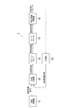
図1は、PLL周波数シンセサイザ1の構成を示す図である。PLL周波数シンセサイザ1は、基準発振器10、位相比較部20、チャージポンプ30、ループフィルタ40、電圧制御発振器50および分周器60を備える。
FIG. 1 is a diagram showing a configuration of a
基準発振器10は、例えば水晶振動子を含み、高精度に安定化された一定周波数の基準発振信号を位相比較部20へ出力する。位相比較部20は、この基準発振信号を入力する。また、位相比較部20は、分周器60から出力される帰還発振信号を入力する。位相比較部20は、これら帰還発振信号と基準発振信号との間の位相差を検出して、この位相差を表す位相差信号をチャージポンプ30へ出力する。位相差信号は、基準発振信号および帰還発振信号のうち何れの信号の位相が進んでいるかを表す。
The
チャージポンプ30は、位相比較部20から出力される位相差信号を入力して、この位相差信号が表す位相差に応じた充放電電流をループフィルタ40へ出力する。チャージポンプ30からループフィルタ40へ出力へ出力される充放電電流は、基準発振信号および帰還発振信号のうち何れの信号の位相が進んでいるかに応じて極性が異なる。ループフィルタ40は、チャージポンプ30から出力される充放電電流を入力して充放電される容量素子を含み、この充放電量に応じて増減される制御電圧値を電圧制御発振器50へ出力する。ループフィルタ40は、容量素子の他に抵抗器をも含む。
The
電圧制御発振器50は、ループフィルタ40から出力される制御電圧値を入力し、この制御電圧値に応じた周波数を有する発振信号を出力する。分周器60は、電圧制御発振器50から出力される発振信号を入力し、この発振信号をN分周して帰還発振信号を生成し、この帰還発振信号を位相比較部20へ出力する。
The voltage controlled
位相比較部20、チャージポンプ30、ループフィルタ40、電圧制御発振器50および分周器60はループを構成している。このループにおいて、位相比較部20に入力される基準発振信号と帰還発振信号との位相差が小さくなるように、チャージポンプ30からループフィルタ40へ充放電電流が入力される。そして、このループの動作が安定した状態では、電圧制御発振器50から出力される発振信号は、基準発振信号の周波数をN倍した周波数を有する。なお、分周器60は設けられなくてもよく、この場合には、電圧制御発振器50から出力される発振信号は、基準発振信号の周波数と同じ周波数を有する。
The
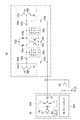
図2は、PLL周波数シンセサイザ1の要部の構成を示す図である。この図には、チャージポンプ30として第1チャージポンプ30Aおよび第2チャージポンプ30Bが示され、また、ループフィルタ40および電圧制御発振器50が示されている。ループフィルタ40は、容量素子41およびアンプ42を含む他、電圧制御発振器50の第1容量素子51a,51bをも含んで構成される。
FIG. 2 is a diagram illustrating a configuration of a main part of the
第1チャージポンプ30Aは、位相比較部20から出力される位相差信号を入力し、この位相差信号が表す位相差に応じた充放電電流Ipを出力する。
The
第2チャージポンプ30Bは、第2容量素子31、第2インバータ回路32および第3インバータ回路33を含む。第2チャージポンプ30Bは、位相比較部20から出力される位相差信号を入力し、インバータ回路33,32からなるバッファを経た位相差信号を、容量素子31を介して出力する。容量素子31はAC結合容量素子として用いられる。
The
容量素子41は、第1チャージポンプ30Aの出力端と接地電位端との間に設けられている。アンプ42は、2つの入力端および1つの出力端を有し、一方の入力端に容量素子41の電圧値が入力され、他方の入力端が出力端に接続されている。アンプ42は、ボルテージフォロワ構成となっている。アンプ42は、容量素子41の電圧値に応じた電圧値を出力端から出力する。
The
容量素子51a,51bと容量素子31との接続点の電圧値Vcは、第1チャージポンプ30Aから出力される充放電電流Ipおよび第2チャージポンプから出力される位相差信号に基づいて設定される。ループフィルタ40は、この接続点の電圧値を制御電圧値として電圧制御発振器50へ与える。
The voltage value Vc at the connection point between the
電圧制御発振器50は、LC-VCOのタイプのものである。電圧制御発振器50は、第1容量素子51a,51b、DCカット容量素子52a,52b、インダクタ素子53a,53b、NMOSトランジスタ54a,54b、可変容量部55a,55b、および、第1インバータ回路56a,56bを含む。
The voltage controlled
容量素子51aと容量素子51bとは互いに同じ電気的特性を有する。DCカット容量素子52aとDCカット容量素子52bとは互いに同じ電気的特性を有する。インダクタ素子53aとインダクタ素子53bとは互いに同じ電気的特性を有する。NMOSトランジスタ54aとNMOSトランジスタ54bとは互いに同じ電気的特性を有する。可変容量部55aと可変容量部55bとは互いに同じ電気的特性を有する。また、インバータ回路56aとインバータ回路56bとは互いに同じ電気的特性を有する。
The
容量素子51a、DCカット容量素子52aおよびインダクタ素子53aは、直列的に順に接続されている。容量素子51aの一端は制御電圧値Vcが入力される。インダクタ素子53aの一端は電源電位VDDが与えられる。NMOSトランジスタ54aのドレインおよび可変容量部55aの一端は、DCカット容量素子52aとインダクタ素子53aとの接続点に接続されている。NMOSトランジスタ54aのソースおよび可変容量部55aの他端は、接地電位が与えられる。
The
容量素子51b、DCカット容量素子52bおよびインダクタ素子53bは、直列的に順に接続されている。容量素子51bの一端は制御電圧値Vcが入力される。インダクタ素子53bの一端は電源電位VDDが与えられる。NMOSトランジスタ54bのドレインおよび可変容量部55bの一端は、DCカット容量素子52bとインダクタ素子53bとの接続点に接続されている。NMOSトランジスタ54bのソースおよび可変容量部55bの他端は、接地電位が与えられる。
The
NMOSトランジスタ54aのゲートは、NMOSトランジスタ54bのドレインと接続されている。NMOSトランジスタ54bのゲートは、NMOSトランジスタ54aのドレインと接続されている。
The gate of the
可変容量部55a,55bそれぞれは、直列的に接続された容量素子およびスイッチを1組として、複数組が並列的に設けられた構成を有している。可変容量部55a,55bそれぞれは、複数のスイッチのうちオン状態のスイッチの個数に応じた容量値を有する。
Each of the
インバータ回路56aの出力端は、容量素子51aとDCカット容量素子52aとの接続点に接続されている。インバータ回路56aは、容量素子51aとDCカット容量素子52aとの接続点を所定のバイアス電位に設定するものである。インバータ回路56aを構成するPMOSトランジスタおよびNMOSトランジスタの双方は動作時にオン状態とされる。
An output terminal of the
インバータ回路56bの出力端は、容量素子51bとDCカット容量素子52bとの接続点に接続されている。インバータ回路56bは、容量素子51bとDCカット容量素子52bとの接続点を所定のバイアス電位に設定するものである。インバータ回路56bを構成するPMOSトランジスタおよびNMOSトランジスタの双方は動作時にオン状態とされる。
The output terminal of the
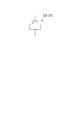
容量素子51a,51bそれぞれは、制御電圧値Vcに応じて変化する容量値を有する。容量素子51a,51bそれぞれは、バラクタであってもよいし、図3に示されるようにMOSトランジスタのドレインとソースとが互いに接続された構成を有するものであってもよい。後者の場合、ドレインとソースとの接続点を一端とし、ゲートを他端とする容量素子が構成される。
Each of the
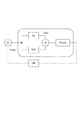
図4は、PLL周波数シンセサイザ1の位相領域モデルを示す図である。PLL周波数シンセサイザ1のオープンループ特性H(s)は下記(1)式で表される。Kvcoは、電圧制御発振器50の特性(制御電圧値に対する発振信号の周波数の依存性)を示す。Kpは、ループフィルタ40の比例項である。Kiは、ループフィルタ40の積分項である。
FIG. 4 is a diagram illustrating a phase domain model of the
![]()
![]()
第2チャージポンプ30Bの容量素子31の容量値をC31とし、電圧制御発振器50の容量素子51a,51bの容量値をC51とする。このとき、比例項Kpは下記(2)式で表される。一般に容量素子31の容量値C31と比べると容量素子51a,51bの容量値C51は非常に大きいので、(2)式は下記(3)式で近似される。
The capacitance of the
![]()
![]()
![]()
![]()
電圧制御発振器50の容量素子51a,51bの容量値C51は制御電圧値Vcに応じて変化する。もし、第2チャージポンプ30Bの容量素子31が例えばMOM(Metal-Oxide-Metal)容量であると、容量素子31の容量値C31は電圧値に依らず一定である。この場合、制御電圧値Vcが変化すると、上記(2)式または(3)式で表される比例項Kpも変化する。制御電圧値Vcによって比例項Kpが変化すると、ジッタが増加する問題が生じ、また、位相合わせが正しく行えなくなる問題が生じて、電圧制御発振器50から出力される発振信号をクロックとして用いる回路が正しく動作しない可能性がある。
The capacitance value C 51 of the
そこで、本実施形態では、第2チャージポンプ30Bの容量素子31は、電圧値に応じて変化する容量値を有するものとされる。容量素子31は、バラクタであってもよいし、図3に示されるようにMOSトランジスタのドレインとソースとが互いに接続された構成を有するものであってもよい。
Therefore, in the present embodiment, the
容量素子51a,51bおよび容量素子31それぞれの電気的特性は互いに同じである。容量素子51a,51bおよび容量素子31それぞれに与えられる電圧値をVとしたとき、電圧値Vでの容量素子51a,51bの容量値C51(V)と容量素子31の容量値C31(V)との比(C51(V)/C31(V))は、電圧値Vの一定範囲(実際の動作における制御電圧値の範囲)において電圧値Vによらず一定である。
The electric characteristics of the
本実施形態では、このようにすることで、制御電圧値Vcが変化しても、上記(2)式または(3)式で表される比例項Kpは一定である。したがって、ジッタの増加が抑制され、また、位相合わせが正しく行われて、電圧制御発振器50から出力される発振信号をクロックとして用いる回路の誤動作が抑制される。したがって、所望の伝達関数を容易に実現することができる。
In this embodiment, the proportional term Kp expressed by the above equation (2) or (3) is constant even if the control voltage value Vc changes in this way. Therefore, an increase in jitter is suppressed, and phase alignment is performed correctly, and malfunction of a circuit that uses an oscillation signal output from the voltage controlled
本発明者による実験によれば、容量素子51a,51bがバラクタであって容量素子31がMOM容量である場合(比較例)では、制御電圧値Vcは113mV±17mV(16%誤差)であった。これに対して、容量素子51a,51bおよび容量素子31がバラクタである場合(実施例)では、制御電圧値Vcは105mV±2mV(2%誤差)であった。このように、比較例と比べて実施例では制御電圧値Vcは安定したものとなった。
According to an experiment by the present inventor, when the
また、本実施形態では、第2チャージポンプ30Bにおいて容量素子31の前段にインバータ回路32が設けられる。その結果、第2チャージポンプ30Bの出力信号は、電源電位または接地電位からのノイズの影響を受ける場合がある。そこで、電圧制御発振器50においては、容量素子51aとDCカット容量素子52aとの接続点がインバータ回路56aにより所定のバイアス電位に設定され、容量素子51bとDCカット容量素子52bとの接続点がインバータ回路56bにより所定のバイアス電位に設定される。インバータ回路56a,56bそれぞれを構成するPMOSトランジスタおよびNMOSトランジスタの双方は動作時にオン状態とされる。このようなインバータ回路56a,56bが設けられることにより、電源電位または接地電位のノイズがバイアス電位に流れ込んで、第2チャージポンプ30Bの出力信号におけるノイズの影響が低減される。
In the present embodiment, the
本実施形態の上記の説明では、ループフィルタ40が容量素子41およびアンプ42を含む構成とした。ループフィルタ40がアンプ42を含む場合、消費電力や半導体基板上の面積が大きくなり、また、ノイズが大きくなってジッタ増加の要因となる。そこで、電圧制御発振器50の容量素子51a,51bの容量値C51が十分に大きい場合、容量素子41を容量素子51a,51bで共用するとともに、アンプ42を設けない構成としてもよい。このようにすることで、消費電力や半導体基板上の面積を小さくすることができ、また、ジッタを低減することができる。
In the above description of the present embodiment, the
本発明は、上記実施形態に限定されるものではなく、種々の変形が可能である。例えば、電圧制御発振器は、様々な構成のものがあり、上記実施形態で説明した構成とは異なる構成のものであってもよい。 The present invention is not limited to the above embodiment, and various modifications can be made. For example, the voltage controlled oscillator has various configurations, and may have a configuration different from the configuration described in the above embodiment.
1…PLL周波数シンセサイザ、10…基準発振器、20…位相比較部、30…チャージポンプ、30A…第1チャージポンプ、30B…第2チャージポンプ、31…第2容量素子、32…第2インバータ回路、40…ループフィルタ、41…容量素子、42…アンプ、50…電圧制御発振器、51a,51b…第1容量素子、52a,52b…DCカット容量素子、53a,53b…インダクタ素子、54a,54b…NMOSトランジスタ、55a,55b…可変容量部、56a,56b…第1インバータ回路、60…分周器。
DESCRIPTION OF
Claims (4)
前記電圧制御発振器から出力される発振信号または該発振信号を分周した信号を帰還発振信号として入力するとともに、基準発振信号をも入力し、これら帰還発振信号と基準発振信号との間の位相差を検出して、この位相差を表す位相差信号を出力する位相比較部と、
前記位相比較部から出力される位相差信号を入力し、この位相差信号が表す位相差に応じた充放電電流を出力する第1チャージポンプと、
前記位相比較部から出力される位相差信号を入力し、この位相差信号の値に応じて変化する容量値を有する第2容量素子をAC結合容量素子として用いて、この第2容量素子を介して前記位相差信号を出力する第2チャージポンプと、
前記第1チャージポンプから出力される充放電電流および前記第2チャージポンプから出力される位相差信号に基づいて設定される前記第1容量素子と前記第2容量素子との接続点の電圧値を前記制御電圧値として前記電圧制御発振器へ与えるループフィルタと、
を備え、
電圧値Vでの前記第1容量素子の容量値と前記第2容量素子の容量値との比は、電圧値Vの一定範囲において電圧値Vによらず一定である、
PLL周波数シンセサイザ。 A voltage controlled oscillator that receives a control voltage value, includes a first capacitance element having a capacitance value that changes according to the control voltage value, and outputs an oscillation signal having a frequency according to the capacitance value of the first capacitance element; ,
An oscillation signal output from the voltage controlled oscillator or a signal obtained by dividing the oscillation signal is input as a feedback oscillation signal, and a reference oscillation signal is also input, and a phase difference between the feedback oscillation signal and the reference oscillation signal And a phase comparison unit that outputs a phase difference signal representing this phase difference,
A first charge pump that inputs a phase difference signal output from the phase comparator and outputs a charge / discharge current corresponding to the phase difference represented by the phase difference signal;
A phase difference signal output from the phase comparison unit is input, and a second capacitance element having a capacitance value that changes in accordance with the value of the phase difference signal is used as an AC coupling capacitance element. A second charge pump for outputting the phase difference signal;
A voltage value at a connection point between the first capacitive element and the second capacitive element, which is set based on a charge / discharge current output from the first charge pump and a phase difference signal output from the second charge pump. A loop filter to be supplied to the voltage controlled oscillator as the control voltage value;
With
The ratio of the capacitance value of the first capacitance element to the capacitance value of the second capacitance element at the voltage value V is constant regardless of the voltage value V in a certain range of the voltage value V.
PLL frequency synthesizer.
請求項1に記載のPLL周波数シンセサイザ。 Each of the first capacitor element and the second capacitor element is a varactor.
The PLL frequency synthesizer according to claim 1.
請求項1に記載のPLL周波数シンセサイザ。 Each of the first capacitive element and the second capacitive element has a configuration in which a drain and a source of a MOS transistor are connected to each other.
The PLL frequency synthesizer according to claim 1.
前記第2チャージポンプが、前記第2容量素子の前段に設けられた第2インバータ回路を含み、
前記第1インバータ回路を構成するPMOSトランジスタおよびNMOSトランジスタの双方が動作時にオン状態とされる、
請求項1〜3の何れか1項に記載のPLL周波数シンセサイザ。 The voltage controlled oscillator includes a DC cut capacitive element connected to the first capacitive element, and a first inverter circuit having an output terminal connected to a connection point between the first capacitive element and the DC cut capacitive element. Including
The second charge pump includes a second inverter circuit provided in front of the second capacitive element;
Both the PMOS transistor and the NMOS transistor constituting the first inverter circuit are turned on during operation.
The PLL frequency synthesizer according to claim 1.
Priority Applications (1)
| Application Number | Priority Date | Filing Date | Title |
|---|---|---|---|
| JP2016082947A JP6746161B2 (en) | 2016-04-18 | 2016-04-18 | PLL frequency synthesizer |
Applications Claiming Priority (1)
| Application Number | Priority Date | Filing Date | Title |
|---|---|---|---|
| JP2016082947A JP6746161B2 (en) | 2016-04-18 | 2016-04-18 | PLL frequency synthesizer |
Publications (2)
| Publication Number | Publication Date |
|---|---|
| JP2017195437A true JP2017195437A (en) | 2017-10-26 |
| JP6746161B2 JP6746161B2 (en) | 2020-08-26 |
Family
ID=60155593
Family Applications (1)
| Application Number | Title | Priority Date | Filing Date |
|---|---|---|---|
| JP2016082947A Active JP6746161B2 (en) | 2016-04-18 | 2016-04-18 | PLL frequency synthesizer |
Country Status (1)
| Country | Link |
|---|---|
| JP (1) | JP6746161B2 (en) |
Citations (3)
| Publication number | Priority date | Publication date | Assignee | Title |
|---|---|---|---|---|
| JPH0232240U (en) * | 1988-08-24 | 1990-02-28 | ||
| JPH10233682A (en) * | 1997-02-20 | 1998-09-02 | Nec Corp | Control voltage generating circuit, pll circuit provided with it and cd-rom driver provided with it |
| JP2011009849A (en) * | 2009-06-23 | 2011-01-13 | Panasonic Corp | Pll frequency synthesizer |
-
2016
- 2016-04-18 JP JP2016082947A patent/JP6746161B2/en active Active
Patent Citations (3)
| Publication number | Priority date | Publication date | Assignee | Title |
|---|---|---|---|---|
| JPH0232240U (en) * | 1988-08-24 | 1990-02-28 | ||
| JPH10233682A (en) * | 1997-02-20 | 1998-09-02 | Nec Corp | Control voltage generating circuit, pll circuit provided with it and cd-rom driver provided with it |
| JP2011009849A (en) * | 2009-06-23 | 2011-01-13 | Panasonic Corp | Pll frequency synthesizer |
Also Published As
| Publication number | Publication date |
|---|---|
| JP6746161B2 (en) | 2020-08-26 |
Similar Documents
| Publication | Publication Date | Title |
|---|---|---|
| US7298183B2 (en) | High frequency divider circuits and methods | |
| CN105743493B (en) | Oscillator with frequency control loop | |
| US20140085011A1 (en) | Supply regulated voltage controlled oscillator including active loop filter and phase locked loop using the same | |
| JP2001119296A (en) | Pll circuit | |
| KR101252048B1 (en) | A Frequency-Phase-Locked Loop with a Self-Noise Suppressing Voltage Controlled Oscillator | |
| CN107528567B (en) | Injection locked oscillator and semiconductor device including the same | |
| JP5876368B2 (en) | Phase-locked loop circuit having a voltage controlled oscillator with improved bandwidth | |
| CN104601168A (en) | Self-biased phase locked loop | |
| CN110784177A (en) | Voltage controlled oscillator, PLL circuit and CDR apparatus | |
| US8547150B2 (en) | Phase-locked loop with two negative feedback loops | |
| US9407137B2 (en) | Charge pump circuit and PLL circuit | |
| KR20120012386A (en) | Lock Detection Circuits and Phase-Locked Loops Comprising the Same | |
| JP5053413B2 (en) | Synchronous circuit | |
| US8786328B2 (en) | RF logic divider | |
| US8970311B2 (en) | Voltage-controlled oscillator with amplitude and frequency independent of process variations and temperature | |
| JP4636107B2 (en) | PLL circuit | |
| JP6746161B2 (en) | PLL frequency synthesizer | |
| US7391275B2 (en) | Circuits and methods for a ring oscillator with adjustable delay and/or resonator tank stage | |
| JP4510039B2 (en) | Phase synchronization circuit | |
| US6985045B2 (en) | Gain control circuits for voltage controlled oscillators | |
| US20090206893A1 (en) | Charge pump circuit and pll circuit | |
| US8598958B1 (en) | Temperature and/or voltage independent voltage controlled oscillator with programmable gain and/or output frequency range | |
| US20100026397A1 (en) | Pll circuit | |
| JP2018074231A (en) | Phase locked loop | |
| CN112886962A (en) | Five-time frequency converter and method thereof |
Legal Events
| Date | Code | Title | Description |
|---|---|---|---|
| A621 | Written request for application examination |
Free format text: JAPANESE INTERMEDIATE CODE: A621 Effective date: 20190416 |
|
| A521 | Request for written amendment filed |
Free format text: JAPANESE INTERMEDIATE CODE: A523 Effective date: 20190524 |
|
| A977 | Report on retrieval |
Free format text: JAPANESE INTERMEDIATE CODE: A971007 Effective date: 20191211 |
|
| A131 | Notification of reasons for refusal |
Free format text: JAPANESE INTERMEDIATE CODE: A131 Effective date: 20200107 |
|
| A521 | Request for written amendment filed |
Free format text: JAPANESE INTERMEDIATE CODE: A523 Effective date: 20200226 |
|
| TRDD | Decision of grant or rejection written | ||
| A01 | Written decision to grant a patent or to grant a registration (utility model) |
Free format text: JAPANESE INTERMEDIATE CODE: A01 Effective date: 20200721 |
|
| A61 | First payment of annual fees (during grant procedure) |
Free format text: JAPANESE INTERMEDIATE CODE: A61 Effective date: 20200731 |
|
| R150 | Certificate of patent or registration of utility model |
Ref document number: 6746161 Country of ref document: JP Free format text: JAPANESE INTERMEDIATE CODE: R150 |
|
| R250 | Receipt of annual fees |
Free format text: JAPANESE INTERMEDIATE CODE: R250 |
|
| R250 | Receipt of annual fees |
Free format text: JAPANESE INTERMEDIATE CODE: R250 |
|
| R250 | Receipt of annual fees |
Free format text: JAPANESE INTERMEDIATE CODE: R250 |