JP2017191594A - Sanitize-aware dram controller - Google Patents
Sanitize-aware dram controller Download PDFInfo
- Publication number
- JP2017191594A JP2017191594A JP2016249420A JP2016249420A JP2017191594A JP 2017191594 A JP2017191594 A JP 2017191594A JP 2016249420 A JP2016249420 A JP 2016249420A JP 2016249420 A JP2016249420 A JP 2016249420A JP 2017191594 A JP2017191594 A JP 2017191594A
- Authority
- JP
- Japan
- Prior art keywords
- block
- dram
- controller
- flag
- blocks
- Prior art date
- Legal status (The legal status is an assumption and is not a legal conclusion. Google has not performed a legal analysis and makes no representation as to the accuracy of the status listed.)
- Granted
Links
Images


Classifications
-
- G—PHYSICS
- G11—INFORMATION STORAGE
- G11C—STATIC STORES
- G11C11/00—Digital stores characterised by the use of particular electric or magnetic storage elements; Storage elements therefor
- G11C11/21—Digital stores characterised by the use of particular electric or magnetic storage elements; Storage elements therefor using electric elements
- G11C11/34—Digital stores characterised by the use of particular electric or magnetic storage elements; Storage elements therefor using electric elements using semiconductor devices
- G11C11/40—Digital stores characterised by the use of particular electric or magnetic storage elements; Storage elements therefor using electric elements using semiconductor devices using transistors
- G11C11/401—Digital stores characterised by the use of particular electric or magnetic storage elements; Storage elements therefor using electric elements using semiconductor devices using transistors forming cells needing refreshing or charge regeneration, i.e. dynamic cells
- G11C11/406—Management or control of the refreshing or charge-regeneration cycles
-
- G—PHYSICS
- G06—COMPUTING; CALCULATING OR COUNTING
- G06F—ELECTRIC DIGITAL DATA PROCESSING
- G06F13/00—Interconnection of, or transfer of information or other signals between, memories, input/output devices or central processing units
- G06F13/14—Handling requests for interconnection or transfer
- G06F13/16—Handling requests for interconnection or transfer for access to memory bus
- G06F13/1605—Handling requests for interconnection or transfer for access to memory bus based on arbitration
- G06F13/161—Handling requests for interconnection or transfer for access to memory bus based on arbitration with latency improvement
- G06F13/1636—Handling requests for interconnection or transfer for access to memory bus based on arbitration with latency improvement using refresh
-
- G—PHYSICS
- G06—COMPUTING; CALCULATING OR COUNTING
- G06F—ELECTRIC DIGITAL DATA PROCESSING
- G06F12/00—Accessing, addressing or allocating within memory systems or architectures
- G06F12/02—Addressing or allocation; Relocation
- G06F12/08—Addressing or allocation; Relocation in hierarchically structured memory systems, e.g. virtual memory systems
- G06F12/0802—Addressing of a memory level in which the access to the desired data or data block requires associative addressing means, e.g. caches
- G06F12/0893—Caches characterised by their organisation or structure
-
- G—PHYSICS
- G06—COMPUTING; CALCULATING OR COUNTING
- G06F—ELECTRIC DIGITAL DATA PROCESSING
- G06F12/00—Accessing, addressing or allocating within memory systems or architectures
- G06F12/14—Protection against unauthorised use of memory or access to memory
-
- G—PHYSICS
- G06—COMPUTING; CALCULATING OR COUNTING
- G06F—ELECTRIC DIGITAL DATA PROCESSING
- G06F3/00—Input arrangements for transferring data to be processed into a form capable of being handled by the computer; Output arrangements for transferring data from processing unit to output unit, e.g. interface arrangements
- G06F3/06—Digital input from, or digital output to, record carriers, e.g. RAID, emulated record carriers or networked record carriers
- G06F3/0601—Interfaces specially adapted for storage systems
- G06F3/0602—Interfaces specially adapted for storage systems specifically adapted to achieve a particular effect
- G06F3/0614—Improving the reliability of storage systems
- G06F3/0619—Improving the reliability of storage systems in relation to data integrity, e.g. data losses, bit errors
-
- G—PHYSICS
- G06—COMPUTING; CALCULATING OR COUNTING
- G06F—ELECTRIC DIGITAL DATA PROCESSING
- G06F3/00—Input arrangements for transferring data to be processed into a form capable of being handled by the computer; Output arrangements for transferring data from processing unit to output unit, e.g. interface arrangements
- G06F3/06—Digital input from, or digital output to, record carriers, e.g. RAID, emulated record carriers or networked record carriers
- G06F3/0601—Interfaces specially adapted for storage systems
- G06F3/0628—Interfaces specially adapted for storage systems making use of a particular technique
- G06F3/0638—Organizing or formatting or addressing of data
- G06F3/064—Management of blocks
-
- G—PHYSICS
- G06—COMPUTING; CALCULATING OR COUNTING
- G06F—ELECTRIC DIGITAL DATA PROCESSING
- G06F3/00—Input arrangements for transferring data to be processed into a form capable of being handled by the computer; Output arrangements for transferring data from processing unit to output unit, e.g. interface arrangements
- G06F3/06—Digital input from, or digital output to, record carriers, e.g. RAID, emulated record carriers or networked record carriers
- G06F3/0601—Interfaces specially adapted for storage systems
- G06F3/0628—Interfaces specially adapted for storage systems making use of a particular technique
- G06F3/0655—Vertical data movement, i.e. input-output transfer; data movement between one or more hosts and one or more storage devices
- G06F3/0659—Command handling arrangements, e.g. command buffers, queues, command scheduling
-
- G—PHYSICS
- G06—COMPUTING; CALCULATING OR COUNTING
- G06F—ELECTRIC DIGITAL DATA PROCESSING
- G06F3/00—Input arrangements for transferring data to be processed into a form capable of being handled by the computer; Output arrangements for transferring data from processing unit to output unit, e.g. interface arrangements
- G06F3/06—Digital input from, or digital output to, record carriers, e.g. RAID, emulated record carriers or networked record carriers
- G06F3/0601—Interfaces specially adapted for storage systems
- G06F3/0668—Interfaces specially adapted for storage systems adopting a particular infrastructure
- G06F3/0671—In-line storage system
- G06F3/0673—Single storage device
-
- G—PHYSICS
- G11—INFORMATION STORAGE
- G11C—STATIC STORES
- G11C11/00—Digital stores characterised by the use of particular electric or magnetic storage elements; Storage elements therefor
- G11C11/21—Digital stores characterised by the use of particular electric or magnetic storage elements; Storage elements therefor using electric elements
- G11C11/34—Digital stores characterised by the use of particular electric or magnetic storage elements; Storage elements therefor using electric elements using semiconductor devices
- G11C11/40—Digital stores characterised by the use of particular electric or magnetic storage elements; Storage elements therefor using electric elements using semiconductor devices using transistors
- G11C11/401—Digital stores characterised by the use of particular electric or magnetic storage elements; Storage elements therefor using electric elements using semiconductor devices using transistors forming cells needing refreshing or charge regeneration, i.e. dynamic cells
- G11C11/406—Management or control of the refreshing or charge-regeneration cycles
- G11C11/40622—Partial refresh of memory arrays
-
- G—PHYSICS
- G11—INFORMATION STORAGE
- G11C—STATIC STORES
- G11C11/00—Digital stores characterised by the use of particular electric or magnetic storage elements; Storage elements therefor
- G11C11/21—Digital stores characterised by the use of particular electric or magnetic storage elements; Storage elements therefor using electric elements
- G11C11/34—Digital stores characterised by the use of particular electric or magnetic storage elements; Storage elements therefor using electric elements using semiconductor devices
- G11C11/40—Digital stores characterised by the use of particular electric or magnetic storage elements; Storage elements therefor using electric elements using semiconductor devices using transistors
- G11C11/401—Digital stores characterised by the use of particular electric or magnetic storage elements; Storage elements therefor using electric elements using semiconductor devices using transistors forming cells needing refreshing or charge regeneration, i.e. dynamic cells
- G11C11/4063—Auxiliary circuits, e.g. for addressing, decoding, driving, writing, sensing or timing
- G11C11/407—Auxiliary circuits, e.g. for addressing, decoding, driving, writing, sensing or timing for memory cells of the field-effect type
- G11C11/409—Read-write [R-W] circuits
-
- G—PHYSICS
- G06—COMPUTING; CALCULATING OR COUNTING
- G06F—ELECTRIC DIGITAL DATA PROCESSING
- G06F2212/00—Indexing scheme relating to accessing, addressing or allocation within memory systems or architectures
- G06F2212/10—Providing a specific technical effect
- G06F2212/1028—Power efficiency
-
- G—PHYSICS
- G06—COMPUTING; CALCULATING OR COUNTING
- G06F—ELECTRIC DIGITAL DATA PROCESSING
- G06F2212/00—Indexing scheme relating to accessing, addressing or allocation within memory systems or architectures
- G06F2212/10—Providing a specific technical effect
- G06F2212/1052—Security improvement
-
- G—PHYSICS
- G11—INFORMATION STORAGE
- G11C—STATIC STORES
- G11C11/00—Digital stores characterised by the use of particular electric or magnetic storage elements; Storage elements therefor
- G11C11/21—Digital stores characterised by the use of particular electric or magnetic storage elements; Storage elements therefor using electric elements
- G11C11/34—Digital stores characterised by the use of particular electric or magnetic storage elements; Storage elements therefor using electric elements using semiconductor devices
- G11C11/40—Digital stores characterised by the use of particular electric or magnetic storage elements; Storage elements therefor using electric elements using semiconductor devices using transistors
- G11C11/401—Digital stores characterised by the use of particular electric or magnetic storage elements; Storage elements therefor using electric elements using semiconductor devices using transistors forming cells needing refreshing or charge regeneration, i.e. dynamic cells
- G11C11/406—Management or control of the refreshing or charge-regeneration cycles
- G11C11/40611—External triggering or timing of internal or partially internal refresh operations, e.g. auto-refresh or CAS-before-RAS triggered refresh
-
- Y—GENERAL TAGGING OF NEW TECHNOLOGICAL DEVELOPMENTS; GENERAL TAGGING OF CROSS-SECTIONAL TECHNOLOGIES SPANNING OVER SEVERAL SECTIONS OF THE IPC; TECHNICAL SUBJECTS COVERED BY FORMER USPC CROSS-REFERENCE ART COLLECTIONS [XRACs] AND DIGESTS
- Y02—TECHNOLOGIES OR APPLICATIONS FOR MITIGATION OR ADAPTATION AGAINST CLIMATE CHANGE
- Y02D—CLIMATE CHANGE MITIGATION TECHNOLOGIES IN INFORMATION AND COMMUNICATION TECHNOLOGIES [ICT], I.E. INFORMATION AND COMMUNICATION TECHNOLOGIES AIMING AT THE REDUCTION OF THEIR OWN ENERGY USE
- Y02D10/00—Energy efficient computing, e.g. low power processors, power management or thermal management
Abstract
Description
関連出願への相互参照
本出願は、参照によりその全体が本明細書に組み込まれる、SANITIZE−AWARE DRAM CONTROLLERと題する米国仮出願第62/323,177号(2006年4月15日出願)に基づく優先権を主張する。
CROSS REFERENCE TO RELATED APPLICATIONS This application is based on US Provisional Application No. 62 / 323,177 (filed April 15, 2006) entitled SANITIZE-AWARE DRAM CONTROLLER, which is incorporated herein by reference in its entirety. Claim priority.
ダイナミック・ランダム・アクセス・メモリ(DRAM)は、現代のコンピューティングシステムにおいて普及している。DRAMは、コストが低く、容量/密度が高く、高速であるため、普及している。密度の利点は、主に、データビットを記憶するための各セルがコンデンサおよび単一トランジスタのみを必要とするという事実に由来する。これは、例えば、スタティック・ランダム・アクセス・メモリ(SRAM)でセル当たりに必要とされるよりも著しく少ないハードウェアである。しかしながら、セルのキャパシタへのデータビットの記憶は、電力消費コストを意味する。これは、コンデンサの電荷が時間とともにリークし、セルに値の喪失を引き起こす。したがって、その値を保持するために、コンデンサは定期的に「リフレッシュ」されねばならない。これは、セルから現在の値を読み取り、その値を「リフレッシュ」するためにセルに書き戻すことを含む。リフレッシュ動作は、リフレッシュを必要としない他のメモリ技術以上の追加の電力を消費する。リフレッシュは、システムによるDRAMアクセスの需要に応じて、DRAMのエネルギー消費のかなりの割合、例えば約20%に寄与し、システム性能を、例えば約30%低下させる可能性がある。 Dynamic random access memory (DRAM) is prevalent in modern computing systems. DRAM is popular because of its low cost, high capacity / density, and high speed. The density advantage stems primarily from the fact that each cell for storing data bits requires only a capacitor and a single transistor. This is, for example, significantly less hardware than is required per cell in static random access memory (SRAM). However, the storage of data bits in the cell capacitor means power consumption costs. This causes the capacitor charge to leak over time, causing the cell to lose value. Therefore, the capacitor must be periodically “refreshed” to hold that value. This involves reading the current value from the cell and writing it back to the cell to “refresh” it. The refresh operation consumes additional power over other memory technologies that do not require refresh. Refresh can contribute to a significant percentage of the DRAM's energy consumption, for example about 20%, and reduce system performance, for example about 30%, depending on the demand for DRAM access by the system.
本発明の共同発明者の一人による米国特許第5,469,559号には、DRAMの有効なデータを含まない選択された部分をリフレッシュするためのメモリコントローラおよび方法が記載されている。これは、無効なデータへの不要なリフレッシュによって消費される電力の量が削減される可能性がある。 US Pat. No. 5,469,559 by one of the co-inventors of the present invention describes a memory controller and method for refreshing selected portions of DRAM that do not contain valid data. This can reduce the amount of power consumed by unnecessary refresh to invalid data.
本発明の発明者らは、さらなる利点を提供するDRAMコントローラの実施形態を提供する。追加の利点は、多くのオペレーティングシステムが、例えばハッカー及び/又はメモリが割り当てられた次のユーザが第1のユーザのデータを見ることを防止することによってシステムセキュリティを高めるために、割り当てを解除されたメモリにゼロに書き込むことによってそのメモリを「サニタイズ」するということを本発明者が見出したことによって主に享受される The inventors of the present invention provide an embodiment of a DRAM controller that provides further advantages. An additional advantage is that many operating systems are de-allocated to increase system security, for example by preventing the next user who has been allocated hackers and / or memory from seeing the first user's data. This is mainly enjoyed by the inventor's finding that the memory is "sanitized" by writing zero to that memory.
DRAMのブロックは、DRAM内の1つ又は複数のストレージユニットであり、DRAMコントローラは、それに対してリフレッシュを選択的にイネーブル又はディセーブルすることができる。例えば、データRAM122の「行」と一般に称されるものがリフレッシュ可能である。いくつかのDRAMでは、例えば、1行は512バイトのストレージである。 A block of DRAM is one or more storage units in the DRAM to which the DRAM controller can selectively enable or disable refresh. For example, what is commonly referred to as a “row” in the data RAM 122 can be refreshed. In some DRAMs, for example, a row is 512 bytes of storage.
DRAMのブロックをサニタイズすることは、ブロック内のすべてのロケーションをゼロ値にクリアすることを意味する。 Sanitizing a block of DRAM means clearing all locations in the block to a zero value.
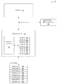
ここで図1を参照すると、コンピューティングシステム100を示すブロック図が示されている。コンピューティングシステム100は、プロセッサ102と、DRAM104と、プロセッサ102をDRAM104に接続するDRAMコントローラ103と、DRAMコントローラ103を介してDRAM104にアクセスする他のバスマスタ106、例えばバスマスタリングI/Oデバイスと、を含む。プロセッサ102は、マルチコアプロセッサであってもよい。プロセッサ102は、オペレーティングシステム及び/又は基本入出力システム(BIOS)又は拡張ファームウェアなどのシステムファームウェア並びにユーティリティ及びアプリケーションプログラムなどのシステムソフトウェアを含むプログラムを実行する。DRAM104は、複数のDRAMブロック142として構成される。システムソフトウェアは、とりわけ、DRAMブロック142全体を含むDRAM104の一部をサニタイズする。多くのオペレーティングシステムは、プロセッサ102にサポートされる仮想メモリシステムに従ってサイズが判定されているページの粒度でメモリをサニタイズする。例えば、共通のページサイズは、4KB、64KB、1MB、16MB、256MB、1GB及び2GBである。
Referring now to FIG. 1, a block diagram illustrating a
DRAMコントローラ103は、DRAMブロック142としての、例えばDRAM104の行のリフレッシュを、DRAMコントローラが選択的にイネーブル又はディセーブルできるDRAM104内の1つ又は複数のストレージの単位を考慮する。いくつかの実施形態では、DRAMブロック142のサイズは、プロセッサ102の仮想メモリシステムによってサポートされる最小のページのサイズに対応する。例えば、DRAMコントローラがリフレッシュを選択的にイネーブル又はディセーブルすることができるストレージの単位が512バイト行であり、プロセッサ102によってサポートされる最小ページサイズが4KBである場合、DRAMコントローラ103は、DRAM104の8つの連続する行をDRAMブロック142として考慮する。
The DRAM controller 103 considers one or more storage units in the
DRAMコントローラ103は、サニタイズビット132とも呼ばれる複数のサニタイズフラグ132及びサニタイズコントローラ134を含む。一実施形態では、DRAMコントローラ103は、DRAM104の対応する各DRAMブロック142について、サニタイズビット132を含む。
The DRAM controller 103 includes a plurality of sanitization flags 132 and
ここではサニタイズ範囲の実施形態と称される代替的実施形態において、各サニタイズビット132は、一緒にサニタイズペアを構成する対応する範囲レジスタを有する。範囲レジスタは、アドレスおよび連続するDRAMブロック142の範囲を指定するカウントを保持する。アドレスは、範囲内の第1または開始のDRAMブロック142を指定し、カウントはその範囲内の連続するDRAMブロック142の数を指定する。サニタイズビット132がセットされている場合、対応する範囲レジスタで指定されたDRAMブロック142の範囲は、以下により詳細に説明するように、サニタイズされたとみなされる。サニタイズコントローラ134は、複数のサニタイズペアを、プールとして扱い、そのプールから一連の連続したDRAMブロック142に対する割り当てを行うことができ(例えば図3のブロック304)、そのプールへ割り当て解除することができる(例えば、図5のブロック508)。サニタイズビット132がセットされている場合、サニタイズペアが割り当てられていることを示し、サニタイズビット132がクリアされている場合、これは、サニタイズペアが割り当てのために空いていることを示す。
In an alternative embodiment, referred to herein as a sanitize range embodiment, each sanitize bit 132 has a corresponding range register that together form a sanitize pair. The range register holds a count that specifies the address and the range of
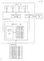
ここで図2を参照すると、代替的実施形態によるコンピューティングシステム100を示すブロック図が示されている。図2のコンピューティングシステム100は、図1のコンピューティングシステム100と類似であり、類似の要素を含む。しかしながら、図2のコンピューティングシステム100では、DRAMコントローラ103がプロセッサ102に組み込まれている。より具体的には、プロセッサ102は、DRAMコントローラ103が接続されたリングバス226を含む。プロセッサ102はまた、リングバス226に接続された複数の処理コア222を含む。プロセッサ102はまた、コア222によって共有されるリングバス226に接続されたラストレベルキャッシュ(LLC)224を含む。好ましくは、DRAMコントローラ103、LLC224、及び各コア222は、それをリングバス226に接続する関連するリングストップ228を有する。最後に、プロセッサ102は、I/Oデバイス106をリングバス226に接続するI/Oリングストップ228を含む。
Referring now to FIG. 2, a block diagram illustrating a
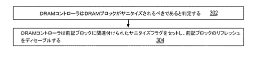
ここで図3を参照すると、システム100の動作を示すフローチャートが示されている。フローはブロック302で開始する。
Referring now to FIG. 3, a flowchart illustrating the operation of the
ブロック302において、DRAMコントローラ103は、DRAMブロック142がサニタイズされるべきであると判定する。一実施形態では、システムソフトウェアは、例えば、図6に関して以下に説明するように、DRAMブロック142がサニタイズされるべきであることをDRAMコントローラ103に通知する。別の実施形態では、DRAMコントローラ103は、例えば、図7および図8に関して以下に説明するように、DRAMブロック142に対するゼロ値書き込みを監視することによって判定を行うハードウェアを含む。DRAMブロック142がサニタイズされるべきであることを判定するための他の実施形態も考えられる。フローはブロック304に進む。
In block 302, the DRAM controller 103 determines that the
ブロック304において、DRAMコントローラ103は、ブロック302で判定されたDRAMブロック142に関連付けられたサニタイズビット132をセットする。さらに、DRAMコントローラ103は、そのDRAMブロック142のリフレッシュをディセーブルする。サニタイズ範囲の実施形態では、DRAMコントローラ103は、サニタイズペアを割り当て、サニタイズビット132をセットし、範囲内の第1のDRAMブロック142のアドレスと、範囲内のDRAMブロック142の数の総数とを範囲レジスタに投入する。さらに、DRAMコントローラ103は、その範囲のすべてのDRAMブロック142のリフレッシュをディセーブルする。フローはブロック304で終了する。
In
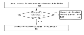
ここで図4を参照すると、システム100の動作を示すフローチャートが示されている。フローはブロック402で開始する。
Referring now to FIG. 4, a flowchart illustrating the operation of the
ブロック402において、DRAMコントローラ103は、DRAM104のロケーションからの読み出し要求を受信する。このロケーションは、DRAMブロック142に関係し、即ちそのアドレスに基づいてDRAMブロック142内にある。フローは判断ブロック404に進む。
In
判断ブロック404において、DRAMコントローラ103は、関係するDRAMブロック142に対応するサニタイズビット132がセットされているかどうかを判定する。そうであれば、フローはブロック408に進み、そうでなければフローはブロック406に進む。サニタイズ範囲の実施形態では、サニタイズコントローラ134は、読み出し要求のアドレスが、サニタイズビット132がセットされたサニタイズペアの範囲レジスタで指定された範囲に入ることを判定する。
At
ブロック406において、DRAMコントローラ103は、指定されたロケーションをDRAM104から読み出し、DRAMコントローラ103の通常動作に従って、読み出されたデータを返す。フローはブロック406で終了する。
In block 406, the DRAM controller 103 reads the specified location from the
ブロック408において、DRAMコントローラ103は、DRAM104を読み出さず、その代わりに読み出し要求にゼロ値を返す。これは、読み出し要求によって関係付けられたDRAMブロック142が判断ブロック404でサニタイズされると判定されたためである。フローはブロック408で終了する。
In block 408, the DRAM controller 103 does not read the
(例えば、ブロック408において)ブロックがサニタイズされているときDRAMを読み取らないことの利点は、(1)ゼロ値を維持するためにDRAMブロックをリフレッシュする必要がないので、より少ない電力が消費されうること、(2)ソフトウェアがデータの読み出しを要求しても、DRAMがデータを読み取るためにアクセスされないので、より少ない電力が消費されうること、(3)要求されたデータを読み取るためにDRAMにアクセスする必要がないので、リード要求の待ち時間が短くなるため性能が向上しうること、があり、それらのすべてはデータの要求されている値がゼロであることが分かっていることにより可能となる。 The advantages of not reading the DRAM when the block is sanitized (eg, at block 408) are that (1) less power can be consumed because the DRAM block does not need to be refreshed to maintain a zero value. (2) Even if software requests to read data, DRAM is not accessed to read data, so less power can be consumed; (3) DRAM is accessed to read requested data There is a need to reduce the latency of read requests and improve performance, all of which can be done by knowing that the requested value of data is zero. .
ここで図5を参照すると、システム100の動作を示すフローチャートが示されている。フローはブロック502で開始する。
Referring now to FIG. 5, a flowchart illustrating the operation of the
ブロック502において、DRAMコントローラ103は、DRAM104のロケーションへのデータ書き込み要求を受信する。より具体的には、DRAMコントローラ103は、書き込まれるデータが非ゼロ値であると判定する。このロケーションは、DRAMブロック142に関係し、即ち、そのアドレスに基づいてDRAMブロック142内にあるか、又は、サニタイズ範囲の実施形態におけるDRAMブロック142の範囲に関係する。代替的実施形態では、DRAMコントローラ103は、書き込まれるデータが非ゼロであるかどうかをチェックするのではなく、代わりにデータ値に関係なく図5の動作を実行する。DRAMコントローラ103がDRAM104のロケーションにゼロ値を有するデータを書き込む要求を受信した場合には、サニタイズビット132がセットされていればDRAMコントローラ103はDRAM104に書き込まないのに対して、サニタイズビット132がクリアされていれば、DRAMコントローラ103がゼロ値をDRAM104の指定されたロケーションに書き込む。フローは判断ブロック504に進む。
In
判断ブロック504において、DRAMコントローラ103は、関係するDRAMブロック142に又はDRAMブロック142の範囲に対応するサニタイズビット132が設定されているかどうかを判定する。そうであれば、フローはブロック508に進む。そうでない場合、フローはブロック506に進む。サニタイズ範囲の実施形態では、サニタイズコントローラ134は、書き込み要求のアドレスが、サニタイズビット132がセットされたサニタイズペアの範囲レジスタに指定された範囲に入ると判定する。
In
ブロック506において、DRAMコントローラ103は、指定されたデータをDRAM104の特定の場所に、即ちDRAMコントローラ103の通常の動作に従って書き込む。フローはブロック506で終了する。
In block 506, the DRAM controller 103 writes the specified data to a specific location in the
ブロック508において、DRAMコントローラ103は、関係するDRAMブロック142に対応するサニタイズビット132をクリアする。さらに、DRAMコントローラ103は、関係するDRAMブロック142のリフレッシュ、又は、サニタイズ範囲の実施形態において範囲レジスタによって関係付けられたDRAMブロック142の範囲のリフレッシュを再びイネーブルする。さらに、DRAMコントローラ103は、指定されたデータをDRAM104の指定されたロケーションに書き込む。最後に、DRAMコントローラ103は、書き込み要求によって指定されたロケーション以外の、DRAMブロック142のすべてのロケーション又はDRAMブロック142の関係する範囲に、ゼロを書き込む。フローはブロック508で終了する。
In
サニタイズされたブロックへの第1の非ゼロ書き込みが行われるまで、ブロックの他のロケーションにゼロ値を書き込むのを待つことの長所は、(1)そのブロックが割り当てられたことをオペレーティングシステムが示すとすぐにリフレッシュが開始される場合(例えば、米国特許第5,469,559号)に比べて、DRAMブロックが追加の回数量だけリフレッシュされず、場合によってそれは、そのブロックが割り当てられた後、ソフトウェアがそのブロックに書き込む前に、かなりの回数量となりうるので、より少ない電力が消費されるかもしれないという点、(2)オペレーティングシステムは、ブロックにゼロを書き込むために、プロセッサ102が数十から数百のオーダーに及びうる命令を実行することを含む、ブロックへのゼロ書き込みを、全ては実行する必要がない、という点である。この後者の考察は、次のよう利点を有する。(a)多くの書き込み命令を実行する必要がないので、プロセッサ102によってより少ない電力が消費される、(b)プロセッサ102が多くの書き込み命令を実行する必要がなくなり、したがって他の命令を実行する空きができるので、システム性能が改善され得る、(c)DRAMコントローラ103は、プロセッサ102が書き込み命令を実行し、かつ、DRAMコントローラ103への書き込み要求を作成しなければならない場合に生じる、余分な待ち時間なしでブロックへのゼロ書き込みを実行するのでシステム性能が改善され得る。第2の利点(2)は、図7及び図8のサニタイズ検出ハードウェア(SDH)の実施形態によっては実現されないことがあると理解されるべきである。 The advantages of waiting for a zero value to be written to another location in the block until the first non-zero write to the sanitized block is done are (1) the operating system indicates that the block has been allocated. Compared to when refreshing begins immediately (eg, US Pat. No. 5,469,559), the DRAM block is not refreshed an additional number of times, possibly after the block is allocated, (2) The operating system has several dozens of processors 102 to write zeros to a block, since less power may be consumed because the software can be a significant amount before writing to that block. To execute a block, including executing instructions that can range from hundreds of orders Zero write, all do not have to run, is that. This latter consideration has the following advantages. (A) less power is consumed by the processor 102 because there is no need to execute many write instructions, (b) the processor 102 does not need to execute many write instructions and therefore executes other instructions The system performance can be improved because there is a free space. (C) The DRAM controller 103 has an extra time that arises when the processor 102 must execute a write instruction and create a write request to the DRAM controller 103. System performance can be improved by performing zero writes to blocks without latency. It should be understood that the second advantage (2) may not be realized by the sanitization detection hardware (SDH) embodiment of FIGS.
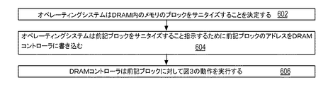
ここで図6を参照すると、一実施形態による、サニタイズされたDRAMブロック142の選択的リフレッシュを実行するシステム100の動作を示すフローチャートが示されている。フローはブロック602で開始する。
Referring now to FIG. 6, a flowchart illustrating the operation of the
ブロック602において、(例えば、オペレーティングシステム又は他のエグゼクティブなどの)システムソフトウェアは、DRAMブロック142をサニタイズすることを判定する。例えば、いくつかのオペレーティングシステムは、メモリロケーションのシークエンス、即ち、所定のメモリアドレスから始まる所定の数の連続するメモリロケーションをサニタイズするために呼び出されるシステムコールであって、UNIX(登録商標)オペレーティングシステム及び、MacOSX並びにMicrosoftWindowsの後のバージョンのような同種のオペレーティングシステムで見られるbzero()やmemset()のようなシステムコールを提供する。慣習的に、それらのシステムコールを実行するルーチンは、所定のシークエンスで全てのメモリロケーションへのゼロ値の一連の書き込みを行う。一実施形態では、システムコールを実行するルーチンは、DRAMコントローラ103の能力を利用して変更される。より具体的には、ルーチンは、1つ又は複数のDRAMブロック142全体が一連のメモリロケーションによって含まれるかどうかをチェックする。そうであれば、従来のように含まれているブロック142への一連のゼロ値書き込みを実行する代わりに、ルーチンは、ブロック604に関して説明するように、DRAMコントローラ103へ、含まれているブロック142をサニタイズするように要求する書き込みをする。フローはブロック604へ進む。
At block 602, system software (eg, an operating system or other executive) determines to sanitize
ブロック604において、システムソフトウェアは、サニタイズすべきブロック142のアドレスをDRAMコントローラ103に書き込む。好ましくは、DRAMコントローラ103は、アドレスを受け取るコントロールレジスタを含む。即ち、コントロールレジスタは、DRAM104及びDRAMコントローラ103を含むシステム100上(例えば、プロセッサ102上)で実行されるシステムソフトウェアによって書き込み可能である。サニタイズ範囲の実施形態では、システムソフトウェアは、アドレス及びその範囲のDRAMブロック142の数の両方を書き込む。フローはブロック606に進む。
In block 604, the system software writes the address of
ブロック606において、DRAMコントローラ103は、指定されたブロック142又はブロック142の範囲に対して図3の動作を実行する、即ち、ブロック142又はブロック142の範囲に関連するサニタイズビット132を設定し、ブロック142又はブロック142の範囲に対してリフレッシュをディセーブルする。フローはブロック606で終了する。
In
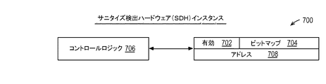
ここで図7を参照すると、サニタイズ検出ハードウェア(SDH)インスタンス700を示すブロック図が示されている。一実施形態では、DRAMコントローラ103は複数のSDHインスタンス700を含み、そこからDRAMコントローラ103が割り当てを行い(例えば、図8のブロック806)、その中へDRAMコントローラ103が割り当てを解除する(例えば、図8のブロック818)。SDHインスタンス700は、有効ビット702、ビットマップ704、アドレスレジスタ708、及びコントロールロジック706を含む。有効ビット702は、真の場合にSDHインスタンス700が割り当てられていることを示し、偽の場合にSDHインスタンス700が空いていることを示す。ビットマップ704は、そのアドレスがアドレスレジスタ708に保持されているDRAMブロック142の各ロケーションに対するビットを含む。様々な実施形態では、DRAMブロック142内のロケーションは、整列バイト、16ビットハーフワード、32ビットワード、64ビットダブルワード、128ビットクワドワード、又は256ビットオクタワードに対応する。一実施形態では、ロケーションは、例えばプロセッサ102のラストレベルキャッシュの整列キャッシュラインに対応する。図8を参照して以下に説明するように、コントロールロジック706は、有効ビット702、ビットマップ704、及び、アドレスレジスタ708の読み出し及び更新に関連する動作を実行する。
Referring now to FIG. 7, a block diagram illustrating a sanitization detection hardware (SDH)
ここで図8を参照すると、図7のSDHインスタンス700を使用することによってDRAMブロック142がサニタイズされることを検出するDRAMコントローラ103の動作を示すフローチャートが示されている。フローはブロック802で開始する。
Referring now to FIG. 8, there is shown a flowchart illustrating the operation of the DRAM controller 103 that detects that the
ブロック802において、DRAMコントローラ103は、DRAM104のロケーションにデータを書き込む要求を受信する。そのロケーションは、DRAMブロック142を表し、即ち、そのアドレスに基づいてDRAMブロック142内にあるか、又は、サニタイズ範囲の実施形態におけるDRAMブロック142を表す。フローは判断ブロック804に進む。
In
判断ブロック804において、DRAMコントローラ103は、SDHインスタンス700が、書き込み要求によって関係付けられたDRAMブロック142又はDRAMブロック142の範囲に対して割り当てられているかどうかを判定する。より具体的には、DRAMコントローラ103は、読み出し要求アドレスの関連部分が、SDHインスタンス700の有効ビット702のアドレス708と一致するかどうかを判定する。そうであれば、フローは判断ブロック808に進み、そうでなければ、フローはブロック806に進む。
At decision block 804, the DRAM controller 103 determines whether the
ブロック806において、サニタイズコントローラ134は空きSDHインスタンス700を割り当てる。好ましくは、SDHインスタンス700を割り当てることは、空きSDHインスタンス700(即ち、有効ビット702が偽である)を見つけること、有効ビットを真に初期化すること、ビットマップ704の全てのビットをゼロへとクリーニングすること、及び、書き込み要求アドレスの関連部分をアドレスレジスタ708に書き込むことを含む。好ましくは、割り当てるべき空きSDH700がない場合、DRAMコントローラ103は単に通常通り継続する、即ち、ブロックがサニタイズされていることを検出することを試みない。フローはブロック806で終了する。
At block 806, the
判断ブロック808において、サニタイズコントローラ134は、書き込まれるべき値がゼロであるかどうかを判定する。そうであれば、フローはブロック814に進む。そうでなければ、フローはブロック812に進む。
At decision block 808, the
ブロック812において、サニタイズコントローラ134は、DRAMブロック142に対して以前に(即ち、ブロック806において)割り当てられたSDHインスタンス700を割り当て解除する。好ましくは、SDHインスタンス700の割り当てを解除することは、後の割り当てのためにSDHインスタンス700を解放する、有効なビット702をクリアすることを含む。フローは、ブロック812で終了する。
At block 812, the
ブロック814において、サニタイズコントローラ134は、ブロック802で受信された要求によって書き込まれたDRAMブロック142内のロケーションに関連するビットマップ704のビットをセットする。フローは、判断ブロック816に進む。
At block 814, the
判断ブロック816において、サニタイズコントローラ134は、ビットマップ704が一杯であるかどうか、即ち、ビットマップ704のビットがすべてセットされているかどうかを判定する。そうであれば、フローはブロック818に進む。そうでなければ、フローは終了する。
At decision block 816, the
ブロック818において、サニタイズコントローラ134は、DRAMブロック142に対して以前に割り当てられたSDHインスタンス700を割り当て解除し、図3を参照して説明したDRAMブロック142の動作の実行を開始する。なぜなら、サニタイズコントローラ134は、システムソフトウェアがDRAMブロック142をサニタイズしたと判定したからである。
At
SDHインスタンスの他の実施形態も考えられる。一実施形態では、DRAMコントローラ103は、ブロック142をサニタイズするための一連のゼロ値書き込みが固定サイズワードであり、ブロック142の第1のロケーションから始まると仮定する。この実施形態はビットマップ704を必要とせず、その代わりに、最も新しくゼロ値が書き込まれたブロック142のワードの後のブロック142内の固定サイズワードのインデックスを保持するレジスタを必要とする。動作中、DRAMコントローラ103は、ブロック142における第1のロケーションへのデータ値の書き込みを検出する。SDHインスタンスがブロック142に対して割り当てられておらず、書き込みが固定サイズのゼロ値ワードである場合、DRAMコントローラ103は、SDHインスタンスを割り当てる。SDHインスタンスの割り当ては、レジスタを1の値に初期化することが含まれる。SDHインスタンスがブロック142に割り当てられている場合、DRAMコントローラ103は、データ値がゼロであり、レジスタのインデックスが現在のゼロ値書き込みのインデックスと一致するかどうかを判定する。そうでなければ、DRAMコントローラ103はSDHインスタンスを割り当て解除する。そうでない場合、DRAMコントローラ103は、レジスタのインデックスがブロック142で最高のインデックスであるかどうかを判定する。そうであれば、DRAMコントローラ103はSDHインスタンスを割り当て解除し、ブロックに対して図3の動作を実行する。そうでなければ、DRAMコントローラ103はレジスタをインクリメントする。
Other embodiments of SDH instances are also conceivable. In one embodiment, DRAM controller 103 assumes that the series of zero value writes to sanitize
本発明の様々な実施形態をここで説明してきたが、それらは例として提示されおり、限定ではないことを理解されたい。関連するコンピュータ技術の当業者には、本発明の範囲から逸脱することなく、形態及び詳細の様々な変更を行うことができることが明らかであろう。例えば、ソフトウェアは、ここで説明された装置及び方法の、例えば、機能、製造、モデリング、シムレーション、ディスクリプション及び/又は試験を可能にすることができる。これは、一般的なプログラミング言語(例えば、C、C++)、VerilogHDL、VHDLなどを含むハードウェア記述言語(HDL)、又は他の利用可能なプログラムを使用して達成することができる。そのようなソフトウェアは、磁気テープ、半導体、磁気ディスク、又は光ディスク(例えば、CD−ROM、DVD−ROMなど)、ネットワーク、有線、無線又は他の通信媒体のような、公知のコンピュータ読取可能媒体に配列され得る。ここで説明された装置及び方法の実施形態は、(例えば、HDLで具体化又は指定され)集積回路の製造においてハードウェアに変換されるプロセッサコアなどの半導体知的財産コアに含まれてもよい。さらに、個々で説明される装置及び方法は、ハードウェアとソフトウェアとの組み合わせとして実施されてもよい。したがって、本発明は、ここで説明された例示的実施形態のいずれによっても制限されるべきではなく、添付の特許請求の範囲及びそれらの均等物に従ってのみ定義されるべきである。具体的には、本発明は、汎用コンピュータで使用可能なプロセッサ装置内で実施することができる。最後に、当業者は、添付の特許請求の範囲によって定義された本発明の範囲を逸脱することなく、本発明と同じ目的を実現するための他の構造を設計し又は改変するための基礎として、開示された概念を容易に使用することができることを評価すべきである。 While various embodiments of the invention have been described herein, it should be understood that they are presented by way of example and not limitation. It will be apparent to those skilled in the relevant computer arts that various changes in form and detail may be made without departing from the scope of the invention. For example, software can enable, for example, functionality, manufacturing, modeling, simulation, description, and / or testing of the devices and methods described herein. This can be accomplished using a hardware programming language (HDL) including common programming languages (eg, C, C ++), Verilog HDL, VHDL, etc., or other available programs. Such software can be on a known computer readable medium, such as magnetic tape, semiconductor, magnetic disk, or optical disk (eg, CD-ROM, DVD-ROM, etc.), network, wired, wireless, or other communication medium. Can be arranged. Embodiments of the apparatus and method described herein may be included in a semiconductor intellectual property core, such as a processor core (eg, embodied or specified in HDL) that is converted to hardware in the manufacture of an integrated circuit. . Further, the individually described devices and methods may be implemented as a combination of hardware and software. Thus, the present invention should not be limited by any of the exemplary embodiments described herein, but should be defined only in accordance with the appended claims and their equivalents. Specifically, the present invention can be implemented in a processor device that can be used in a general-purpose computer. Finally, those skilled in the art will serve as a basis for designing or modifying other structures to achieve the same purpose as the present invention without departing from the scope of the present invention as defined by the appended claims. It should be appreciated that the disclosed concept can be readily used.
Claims (20)
当該DRAMコントローラは、
それぞれが前記DRAMの複数のブロックのうちの1つのブロックと関連する複数のフラグと、
前記複数のブロックのうちの1つのブロックがサニタイズされるべきであると判定し、それに応答して前記複数のブロックのうちの1つのブロックと関連する、前記複数のフラグのうちの1つのフラグをセットし、該ブロックのリフレッシュをディセーブルするサニタイズコントローラと、を含み、
引き続く前記ブロック内のロケーションからのデータ読み取り要求の受信に応答して、前記フラグがクリアされている場合には、当該DRAMコントローラは前記ロケーションを読み出し、そこから読み出されたデータを返し、前記フラグがセットされている場合には、当該DRAMコントローラはゼロ値を返し、DRAMの読み出しを行わない、DRAMコントローラ。 A DRAM controller for controlling a dynamic random access memory (DRAM) including a plurality of blocks, wherein the blocks are one or more storage units in the DRAM, the DRAM controller being connected to the DRAM Refresh can be selectively enabled or disabled,
The DRAM controller is
A plurality of flags each associated with a block of the plurality of blocks of the DRAM;
Determining that one of the plurality of blocks should be sanitized, and in response, determining one flag of the plurality of flags associated with one block of the plurality of blocks; A sanitizing controller that sets and disables refreshing of the block; and
If the flag is cleared in response to receiving a subsequent data read request from a location in the block, the DRAM controller reads the location, returns the data read from it, and returns the flag If is set, the DRAM controller returns a zero value and does not read the DRAM.
(a)前記フラグがクリアされている場合には、当該DRAMコントローラは前記データを前記ロケーションに書き込み、
(b)前記フラグがセットされている場合には、当該DRAMコントローラは前記ブロックのリフレッシュをイネーブルし、前記データを前記ロケーションへ書き込むことをさらに含む、請求項1記載のDRAMコントローラ。 In response to receiving a subsequent data write request to a location in the block,
(A) If the flag is cleared, the DRAM controller writes the data to the location;
The DRAM controller of claim 1, further comprising: (b) if the flag is set, the DRAM controller further enables refresh of the block and writes the data to the location.
(b)前記フラグがセットされている場合には、当該DRAMコントローラはさらに前記フラグをクリアし、前記ブロック内の全ての他のロケーションにゼロ値を書き込むことをさらに含む、請求項2記載のDRAMコントローラ。 In response to receiving a subsequent data write request to the location in the block,
3. The DRAM of claim 2, further comprising: (b) if the flag is set, the DRAM controller further clears the flag and writes a zero value to all other locations in the block. controller.
前記フラグがセットされている場合には、当該DRAMコントローラは、書き込まれるべきデータが非ゼロである場合にのみ、動作(a)及び(b)を実行することをさらに含む、請求項2記載のDRAMコントローラ。 In response to receiving a subsequent data write request to the location in the block,
3. The DRAM controller of claim 2, further comprising: when the flag is set, the DRAM controller performs operations (a) and (b) only when the data to be written is non-zero. DRAM controller.
前記サニタイズコントローラは、前記DRAM及び当該DRAMコントローラを含むシステムのシステムソフトウェアにより前記コントロールレジスタへの書き込みを検出することによって、前記ブロックがサニタイズされるべきであると判定する、請求項1に記載のDRAMコントローラ。 A control register;
The DRAM of claim 1, wherein the sanitization controller determines that the block should be sanitized by detecting a write to the control register by system software of the DRAM and a system including the DRAM controller. controller.
前記DRAMの前記複数のブロックの異なるブロックに対し、前記サニタイズコントローラによって別個に割り当て可能な複数のサニタイズ検出ハードウェアインスタンスを含む、請求項6記載のDRAMコントローラ。 The hardware is
The DRAM controller of claim 6, comprising a plurality of sanitization detection hardware instances that are separately assignable by the sanitization controller to different blocks of the plurality of blocks of the DRAM.
DRAMコントローラがブロック内のどのロケーションにゼロ値が書き込まれたかを追跡するために使用するビットマップと、
前記ビットマップが全て真のビットを有するときを検出するロジックとを備える、請求項7に記載のDRAMコントローラ。 Each sanitization detection hardware instance
A bitmap that the DRAM controller uses to track where in the block the zero value was written;
8. A DRAM controller according to claim 7, comprising logic for detecting when said bitmap has all true bits.
最も新しくゼロ値が書き込まれた前記ブロック内の固定サイズのワードの後の次の固定長のワードのインデックスを保持するレジスタであって、当該インデックスが現在のゼロ値の固定長ワード書き込みのインデックスと一致するとインクリメントされるレジスタと、
前記現在のゼロ値の固定長ワード書き込みのインデックスが前記ブロック内の最高インデックスとなるときを検出するロジックとを備える、請求項7に記載のDRAMコントローラ。 Each sanitization detection hardware instance
A register holding the index of the next fixed-length word after the fixed-size word in the block in which the most recent zero value has been written, the index being the index of the current zero-value fixed-length word write A register that is incremented when matched, and
8. A DRAM controller according to claim 7, comprising logic for detecting when the current zero-value fixed-length word write index is the highest index in the block.
当該方法は、
前記複数のブロックのうちの1つのブロックがサニタイズされるべきであると判定するステップであり、それに応答して、前記複数のブロックのうちの1つのブロックと関連するフラグをセットし、該ブロックのリフレッシュをディセーブルする、判定ステップを備え、
前記フラグは、それぞれがDRAMの複数のブロックのうちの1つのブロックと関連する複数のフラグのうちの1つのフラグであり、
当該方法はさらに、
引き続く前記ブロック内のロケーションからのデータ読み取り要求の受信に応答して、
前記フラグがクリアされている場合に、前記ロケーションを読み出し、そこから読み取られたデータを返すステップと、
前記フラグがセットされている場合に、前記DRAMの読み出しを行わず、ゼロ値を返すステップと、を備える方法。 A method for controlling a dynamic random access memory (DRAM) comprising a plurality of blocks, wherein the blocks are one or more storage units in the DRAM, and a DRAM controller performs refresh on the DRAM. Can be selectively enabled or disabled,
The method is
Determining that a block of the plurality of blocks should be sanitized, and in response, setting a flag associated with one block of the plurality of blocks, A determination step for disabling refresh;
The flag is one of a plurality of flags each associated with a block of the plurality of blocks of the DRAM;
The method further includes:
In response to receiving a subsequent data read request from a location in the block,
Reading the location and returning data read therefrom if the flag is cleared;
Returning a zero value without reading the DRAM when the flag is set.
(a)前記フラグがクリアされている場合に、前記データを前記ロケーションに書き込むステップと、
(b)前記フラグがセットされている場合に、前記ブロックのリフレッシュをイネーブルし、前記ロケーションに前記データを書き込むステップと、をさらに備える、請求項10に記載の方法。 In response to receiving a subsequent data read request from a location in the block,
(A) if the flag is cleared, writing the data to the location;
11. The method of claim 10, further comprising: (b) enabling refresh of the block and writing the data to the location if the flag is set.
(b)前記フラグがセットされている場合に、さらに、前記フラグをクリアし、前記ブロック内の全ての他のロケーションにゼロ値を書き込むステップをさらに備える、請求項11に記載の方法。 In response to receiving a subsequent data read request from a location in the block,
The method of claim 11, further comprising: (b) clearing the flag and writing a zero value to all other locations in the block if the flag is set.
前記フラグがセットされている場合に、書き込まれるべきデータが非ゼロである場合にのみ、動作(a)及び(b)を実行するステップをさらに備える、請求項11に記載の方法。 In response to receiving a subsequent data read request from a location in the block,
12. The method of claim 11, further comprising performing operations (a) and (b) only if the data to be written is non-zero when the flag is set.
前記ブロックがサニタイズされるべきであると判定する判定ステップは、前記ビットマップが全て真のビットを有することを検出するステップをさらに備える、請求項16に記載の方法。 Setting a bit of the bitmap to true in response to detecting a zero value write to a location in the block, wherein each bit of the bitmap is associated with a different location in the block Further comprising
The method of claim 16, wherein determining that the block is to be sanitized further comprises detecting that the bitmap has all true bits.
前記ブロックがサニタイズされるべきであると判定する前記判定ステップは、前記現在のゼロ値の固定長ワード書き込みのインデックスが前記ブロック内の最高インデックスとなるときを検出するステップを備える、請求項16に記載の方法。 If the index matches the current zero-value fixed-length word write index, then by incrementing the register, the index of the next fixed-length word after the most recently written fixed-size word in the block Further comprising maintaining the register to hold
The determination step of determining that the block should be sanitized comprises detecting when the current zero-value fixed-length word write index is the highest index in the block. The method described.
当該コンピュータプログラムは、
複数のブロックを含むダイナミック・ランダム・アクセス・メモリ(DRAM)を制御するためのコントローラを指定するための前記媒体内に具現化されたコンピュータ使用可能プログラムコードを含み、ブロックは前記DRAM内の1つ又は複数のストレージ・ユニットであり、DRAMコントローラは前記DRAMに対するリフレッシュを選択的にイネーブル又はディセーブルすることができ、
前記コンピュータ使用可能プログラムコードは、
それぞれが前記DRAMの複数のブロックのうちの1つのブロックと関連する複数のフラグを指定する第1のプログラムコードと、
前記複数のブロックのうちの1つのブロックがサニタイズされるべきであると判定し、それに応答して前記複数のブロックのうちの1つのブロックと関連する、前記複数のフラグのうちの1つのフラグをセットし、該ブロックのリフレッシュをディセーブルするサニタイズコントローラを指定する第2のプログラムコードとを備え、
引き続く前記ブロック内のロケーションからのデータ読み取り要求の受信に応答して、前記フラグがクリアされている場合に、当該DRAMコントローラは前記ロケーションを読み出し、そこから読み出されたデータを返し、前記フラグがセットされている場合に、当該DRAMコントローラはDRAMの読み出しを行わず、ゼロ値を返す、コンピュータプログラム。 A computer program encoded in at least one non-volatile computer-usable medium for use with a computing device comprising:
The computer program is
Computer-usable program code embodied in the medium for designating a controller for controlling a dynamic random access memory (DRAM) comprising a plurality of blocks, wherein the blocks are one in the DRAM Or a plurality of storage units, the DRAM controller can selectively enable or disable refresh for the DRAM,
The computer usable program code is:
First program code each specifying a plurality of flags associated with one of the plurality of blocks of the DRAM;
Determining that one of the plurality of blocks should be sanitized, and in response, determining one flag of the plurality of flags associated with one block of the plurality of blocks; A second program code for setting and designating a sanitizing controller to disable refreshing of the block;
In response to receiving a subsequent data read request from a location in the block, if the flag is cleared, the DRAM controller reads the location, returns the data read from it, and the flag is A computer program in which, if set, the DRAM controller does not read DRAM and returns a zero value.
Applications Claiming Priority (4)
| Application Number | Priority Date | Filing Date | Title |
|---|---|---|---|
| US201662323177P | 2016-04-15 | 2016-04-15 | |
| US62/323,177 | 2016-04-15 | ||
| US15/335,141 | 2016-10-26 | ||
| US15/335,141 US9972375B2 (en) | 2016-04-15 | 2016-10-26 | Sanitize-aware DRAM controller |
Publications (2)
| Publication Number | Publication Date |
|---|---|
| JP2017191594A true JP2017191594A (en) | 2017-10-19 |
| JP6373336B2 JP6373336B2 (en) | 2018-08-15 |
Family
ID=57838118
Family Applications (1)
| Application Number | Title | Priority Date | Filing Date |
|---|---|---|---|
| JP2016249420A Active JP6373336B2 (en) | 2016-04-15 | 2016-12-22 | Sanitize recognition DRAM controller |
Country Status (5)
| Country | Link |
|---|---|
| US (1) | US9972375B2 (en) |
| EP (1) | EP3232330B1 (en) |
| JP (1) | JP6373336B2 (en) |
| KR (1) | KR101902650B1 (en) |
| CN (1) | CN106782642B (en) |
Families Citing this family (16)
| Publication number | Priority date | Publication date | Assignee | Title |
|---|---|---|---|---|
| US10783146B2 (en) | 2016-07-19 | 2020-09-22 | Sap Se | Join operations in hybrid main memory systems |
| US10540098B2 (en) | 2016-07-19 | 2020-01-21 | Sap Se | Workload-aware page management for in-memory databases in hybrid main memory systems |
| US10698732B2 (en) * | 2016-07-19 | 2020-06-30 | Sap Se | Page ranking in operating system virtual pages in hybrid memory systems |
| US10474557B2 (en) | 2016-07-19 | 2019-11-12 | Sap Se | Source code profiling for line-level latency and energy consumption estimation |
| US10387127B2 (en) | 2016-07-19 | 2019-08-20 | Sap Se | Detecting sequential access data and random access data for placement on hybrid main memory for in-memory databases |
| US10437798B2 (en) | 2016-07-19 | 2019-10-08 | Sap Se | Full system simulator and memory-aware splay tree for in-memory databases in hybrid memory systems |
| US10452539B2 (en) | 2016-07-19 | 2019-10-22 | Sap Se | Simulator for enterprise-scale simulations on hybrid main memory systems |
| US10185509B1 (en) | 2017-06-01 | 2019-01-22 | Amazon Technologies, Inc. | Secure storage device sanitization |
| US11010379B2 (en) | 2017-08-15 | 2021-05-18 | Sap Se | Increasing performance of in-memory databases using re-ordered query execution plans |
| US11182106B2 (en) * | 2018-03-21 | 2021-11-23 | Arm Limited | Refresh circuit for use with integrated circuits |
| US11143684B2 (en) | 2019-03-25 | 2021-10-12 | Lg Energy Solution, Ltd. | Diagnostic system for a vehicle electrical system |
| US10996279B2 (en) | 2019-04-08 | 2021-05-04 | Lg Chem, Ltd. | Diagnostic system for a battery management system |
| US11221949B2 (en) * | 2020-02-10 | 2022-01-11 | Micron Technology, Inc. | Multi state purgatory for media management for a memory subsystem |
| US11442654B2 (en) * | 2020-10-15 | 2022-09-13 | Microsoft Technology Licensing, Llc | Managing and ranking memory resources |
| KR20230000690A (en) | 2021-06-25 | 2023-01-03 | 삼성전자주식회사 | Storage device performing adaptive write/read control and Operating method thereof |
| US20230236985A1 (en) * | 2022-01-21 | 2023-07-27 | Centaur Technology, Inc. | Memory controller zero cache |
Citations (5)
| Publication number | Priority date | Publication date | Assignee | Title |
|---|---|---|---|---|
| US5469559A (en) * | 1993-07-06 | 1995-11-21 | Dell Usa, L.P. | Method and apparatus for refreshing a selected portion of a dynamic random access memory |
| JP2013080560A (en) * | 2006-04-28 | 2013-05-02 | Mosaid Technologies Inc | Dynamic random access memory with fully independent partial array refresh function |
| WO2013183155A1 (en) * | 2012-06-07 | 2013-12-12 | 富士通株式会社 | Control device that selectively refreshes memory |
| JP2014197446A (en) * | 2007-07-26 | 2014-10-16 | クゥアルコム・インコーポレイテッドQualcomm Incorporated | System and method to reduce dynamic ram power consumption via use of valid data indicators |
| WO2014186229A1 (en) * | 2013-05-14 | 2014-11-20 | Qualcomm Incorporated | Methods and systems for smart refresh of dynamic random access memory |
Family Cites Families (14)
| Publication number | Priority date | Publication date | Assignee | Title |
|---|---|---|---|---|
| US5524248A (en) | 1993-07-06 | 1996-06-04 | Dell Usa, L.P. | Random access memory power management system |
| CN100452239C (en) * | 2003-04-24 | 2009-01-14 | 富士通微电子株式会社 | Semiconductor memory |
| US20060181949A1 (en) | 2004-12-31 | 2006-08-17 | Kini M V | Operating system-independent memory power management |
| US7292490B1 (en) | 2005-09-08 | 2007-11-06 | Gsi Technology, Inc. | System and method for refreshing a DRAM device |
| US20070180187A1 (en) | 2006-02-01 | 2007-08-02 | Keith Olson | Reducing power consumption by disabling refresh of unused portions of DRAM during periods of device inactivity |
| JP4299848B2 (en) * | 2006-08-09 | 2009-07-22 | エルピーダメモリ株式会社 | Semiconductor memory device |
| US7613061B2 (en) | 2007-11-30 | 2009-11-03 | Agere Systems Inc. | Method and apparatus for idle cycle refresh request in DRAM |
| US20090172251A1 (en) | 2007-12-26 | 2009-07-02 | Unity Semiconductor Corporation | Memory Sanitization |
| US9501705B2 (en) | 2009-12-15 | 2016-11-22 | Micron Technology, Inc. | Methods and apparatuses for reducing power consumption in a pattern recognition processor |
| US20130036256A1 (en) * | 2011-08-05 | 2013-02-07 | Hitachi, Ltd. | Method and apparatus of sanitizing storage device |
| KR101155451B1 (en) * | 2011-08-31 | 2012-06-15 | 테세라, 인코포레이티드 | Dram security erase |
| US9275696B2 (en) * | 2012-07-26 | 2016-03-01 | Empire Technology Development Llc | Energy conservation in a multicore chip |
| US10157657B2 (en) | 2012-08-28 | 2018-12-18 | Rambus Inc. | Selective refresh with software components |
| US9990293B2 (en) * | 2014-08-12 | 2018-06-05 | Empire Technology Development Llc | Energy-efficient dynamic dram cache sizing via selective refresh of a cache in a dram |
-
2016
- 2016-10-26 US US15/335,141 patent/US9972375B2/en active Active
- 2016-12-13 EP EP16203900.2A patent/EP3232330B1/en active Active
- 2016-12-14 KR KR1020160170134A patent/KR101902650B1/en active IP Right Grant
- 2016-12-22 JP JP2016249420A patent/JP6373336B2/en active Active
-
2017
- 2017-01-10 CN CN201710018716.8A patent/CN106782642B/en active Active
Patent Citations (5)
| Publication number | Priority date | Publication date | Assignee | Title |
|---|---|---|---|---|
| US5469559A (en) * | 1993-07-06 | 1995-11-21 | Dell Usa, L.P. | Method and apparatus for refreshing a selected portion of a dynamic random access memory |
| JP2013080560A (en) * | 2006-04-28 | 2013-05-02 | Mosaid Technologies Inc | Dynamic random access memory with fully independent partial array refresh function |
| JP2014197446A (en) * | 2007-07-26 | 2014-10-16 | クゥアルコム・インコーポレイテッドQualcomm Incorporated | System and method to reduce dynamic ram power consumption via use of valid data indicators |
| WO2013183155A1 (en) * | 2012-06-07 | 2013-12-12 | 富士通株式会社 | Control device that selectively refreshes memory |
| WO2014186229A1 (en) * | 2013-05-14 | 2014-11-20 | Qualcomm Incorporated | Methods and systems for smart refresh of dynamic random access memory |
Also Published As
| Publication number | Publication date |
|---|---|
| US9972375B2 (en) | 2018-05-15 |
| CN106782642A (en) | 2017-05-31 |
| KR20170118583A (en) | 2017-10-25 |
| EP3232330A1 (en) | 2017-10-18 |
| CN106782642B (en) | 2020-02-07 |
| JP6373336B2 (en) | 2018-08-15 |
| EP3232330B1 (en) | 2018-11-07 |
| US20170301386A1 (en) | 2017-10-19 |
| KR101902650B1 (en) | 2018-09-28 |
Similar Documents
| Publication | Publication Date | Title |
|---|---|---|
| JP6373336B2 (en) | Sanitize recognition DRAM controller | |
| US9189415B2 (en) | EDRAM refresh in a high performance cache architecture | |
| US20120137074A1 (en) | Method and apparatus for stream buffer management instructions | |
| US8312227B2 (en) | Method and apparatus for MPI program optimization | |
| CN104252392A (en) | Method for accessing data cache and processor | |
| CN109952565B (en) | Memory access techniques | |
| KR101414035B1 (en) | Storage efficient sectored cache | |
| US8583873B2 (en) | Multiport data cache apparatus and method of controlling the same | |
| US20080162782A1 (en) | Using Transacted Writes and Caching Mechanism to Improve Write Performance in Multi-Level Cell Flash Memory | |
| BR112015001988B1 (en) | Method and equipment for mapping virtual addresses to physical addresses, and computer-readable memory | |
| US9135187B2 (en) | Apparatus and method for protecting memory in multi-processor system | |
| EP2761435A1 (en) | Cache and/or socket sensitive multi-processor cores breadth-first traversal | |
| US10324760B2 (en) | Leases for blocks of memory in a multi-level memory | |
| US11003606B2 (en) | DMA-scatter and gather operations for non-contiguous memory | |
| KR20140018413A (en) | Method and system for safe enqueuing of events | |
| US9063667B2 (en) | Dynamic memory relocation | |
| CN116501249A (en) | Method for reducing repeated data read-write of GPU memory and related equipment | |
| US9904622B2 (en) | Control method for non-volatile memory and associated computer system | |
| WO2015133643A1 (en) | Cache memory with variable write pulse width | |
| WO2018094620A1 (en) | Memory allocation method and apparatus | |
| US9092486B2 (en) | Extensible I/O activity logs | |
| CN113253939B (en) | Data processing method, device, electronic equipment and storage medium | |
| JP2018500697A (en) | Method and apparatus for detecting transaction conflicts and computer system | |
| CN110196819B (en) | Memory access method and hardware | |
| US8521951B2 (en) | Content addressable memory augmented memory |
Legal Events
| Date | Code | Title | Description |
|---|---|---|---|
| A131 | Notification of reasons for refusal |
Free format text: JAPANESE INTERMEDIATE CODE: A131 Effective date: 20171128 |
|
| A521 | Request for written amendment filed |
Free format text: JAPANESE INTERMEDIATE CODE: A523 Effective date: 20180227 |
|
| TRDD | Decision of grant or rejection written | ||
| A01 | Written decision to grant a patent or to grant a registration (utility model) |
Free format text: JAPANESE INTERMEDIATE CODE: A01 Effective date: 20180619 |
|
| A61 | First payment of annual fees (during grant procedure) |
Free format text: JAPANESE INTERMEDIATE CODE: A61 Effective date: 20180717 |
|
| R150 | Certificate of patent or registration of utility model |
Ref document number: 6373336 Country of ref document: JP Free format text: JAPANESE INTERMEDIATE CODE: R150 |
|
| R250 | Receipt of annual fees |
Free format text: JAPANESE INTERMEDIATE CODE: R250 |
|
| R250 | Receipt of annual fees |
Free format text: JAPANESE INTERMEDIATE CODE: R250 |
|
| R250 | Receipt of annual fees |
Free format text: JAPANESE INTERMEDIATE CODE: R250 |