JP2017191202A - Optical element and manufacturing method therefor - Google Patents
Optical element and manufacturing method therefor Download PDFInfo
- Publication number
- JP2017191202A JP2017191202A JP2016080324A JP2016080324A JP2017191202A JP 2017191202 A JP2017191202 A JP 2017191202A JP 2016080324 A JP2016080324 A JP 2016080324A JP 2016080324 A JP2016080324 A JP 2016080324A JP 2017191202 A JP2017191202 A JP 2017191202A
- Authority
- JP
- Japan
- Prior art keywords
- substrate
- electrode
- segment
- uneven
- electrodeposition
- Prior art date
- Legal status (The legal status is an assumption and is not a legal conclusion. Google has not performed a legal analysis and makes no representation as to the accuracy of the status listed.)
- Granted
Links
Images

Landscapes
- Electrochromic Elements, Electrophoresis, Or Variable Reflection Or Absorption Elements (AREA)
Abstract
Description
本発明は、エレクトロデポジション素子を用いた光学素子、および、当該光学素子の製造方法に関する。 The present invention relates to an optical element using an electrodeposition element and a method for manufacturing the optical element.
特許文献1,2には、いわゆるエレクトロデポジション素子が開示されている。エレクトロデポジション素子は、主に、対向配置される一対の透明電極と、その一対の透明電極に挟持され、銀を含むエレクトロデポジション材料を含有する電解質層と、を有する。さらに、一対の透明電極の一方の表面には、多数の微粒子が堆積してなる粒子修飾電極が設けられる。 Patent Documents 1 and 2 disclose so-called electrodeposition elements. The electrodeposition element mainly has a pair of transparent electrodes arranged opposite to each other and an electrolyte layer sandwiched between the pair of transparent electrodes and containing an electrodeposition material containing silver. Furthermore, a particle modifying electrode formed by depositing a large number of fine particles is provided on one surface of the pair of transparent electrodes.
電解質層はほぼ透明であり、定常時(電圧無印加時)、エレクトロデポジション素子は光透過状態(透明状態)となる。一対の透明電極間に直流電圧を印加すると、電気化学反応(酸化・還元反応)により、電解質層のエレクトロデポジション材料(銀など)が、電極上に析出・堆積する。粒子修飾電極が設けられた比較的凸凹な電極の表面にエレクトロデポジション材料が析出・堆積すると、当該エレクトロデポジション材料のプラズモン吸収により、エレクトロデポジション素子は光吸収状態(遮光状態)となる。また、比較的平坦な電極の表面にエレクトロデポジション材料が析出・堆積すると、当該エレクトロデポジション材料(銀など)は鏡面を構成し、エレクトロデポジション素子は光反射状態(鏡面状態)となる。 The electrolyte layer is almost transparent, and the electrodeposition element is in a light transmission state (transparent state) at a steady state (when no voltage is applied). When a DC voltage is applied between the pair of transparent electrodes, an electrodeposition material (such as silver) of the electrolyte layer is deposited and deposited on the electrodes by an electrochemical reaction (oxidation / reduction reaction). When the electrodeposition material is deposited and deposited on the surface of the relatively uneven electrode provided with the particle modification electrode, the electrodeposition element is in a light absorption state (light-blocking state) due to plasmon absorption of the electrodeposition material. Further, when an electrodeposition material is deposited and deposited on the surface of a relatively flat electrode, the electrodeposition material (such as silver) forms a mirror surface, and the electrodeposition element is in a light reflection state (mirror surface state).
本発明の目的は、主に、エレクトロデポジション素子を用いた、信頼性が高い光学素子を提供することにある。 An object of the present invention is mainly to provide a highly reliable optical element using an electrodeposition element.
本発明の主な観点によれば、対向配置される第1および第2の基板と、前記第1の基板の、前記第2の基板との対向面に配置される第1の電極であって、表面に一体的に形成された凸凹構造を含む第1の電極と、前記第2の基板の、前記第1の基板との対向面に配置される第2の電極と、前記第1および第2の基板の間隙に、銀を含むエレクトロデポジション材料を含有する電解質層と、を有する光学素子、が提供される。 According to a main aspect of the present invention, there are first and second substrates disposed opposite to each other, and a first electrode disposed on a surface of the first substrate facing the second substrate. A first electrode including an uneven structure integrally formed on the surface; a second electrode disposed on a surface of the second substrate facing the first substrate; and the first and first electrodes An optical element having an electrolyte layer containing an electrodeposition material containing silver in a gap between two substrates is provided.
信頼性が高い光学素子を得ることができる。 An optical element with high reliability can be obtained.
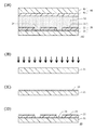
最初に、参考例によるエレクトロデポジション素子(ED素子)を参照して、ED素子の基本的な動作について説明する。 First, the basic operation of the ED element will be described with reference to an electrodeposition element (ED element) according to a reference example.
図1Aは、参考例によるED素子110を示す断面図である。ED素子110は、主に、対向配置される下側および上側基板80,90と、下側および上側基板80,90に挟持されるシール枠部材40および電解質層(電解液)50と、を備える。
FIG. 1A is a cross-sectional view showing an
下側基板80は、支持基板81の表面全面に、透明電極82および装飾電極83が順次積層する構造を有する。また、上側基板90は、支持基板91の表面全面に、透明電極92が積層する構造を有する。透明電極82(ないし装飾電極83)および透明電極92は、相互に対向するように配置されている。
The
支持基板81,91には、透光性を有する基板が用いられ、たとえば、青板ガラスなどのプレート基板や、ポリカーボネートなどにより構成されるフィルム基板などが用いられる。透明電極82,92は、たとえばインジウム錫酸化物(ITO)やインジウム亜鉛酸化物(IZO)など、透光性および導電性を有する部材により構成される。なお、透明電極82,92は、所定の平面形状にパターニングされていてもよい。
As the
装飾電極83は、ナノメートルサイズの微粒子が堆積することにより構成される。装飾電極83は、全体として微細な凹凸形状を有しており、少なくとも透明電極82,92の表面よりも粗くなっている。装飾電極83を構成する微粒子は、透光性および導電性を有する部材、たとえばITO等を含む。なお、透明電極82が所定の平面形状にパターニングされている場合には、一般に、装飾電極83も透明電極82の平面形状に対応してパターニングされる。
The
シール枠部材40は、樹脂などで構成され、下側ないし上側基板80,90面内において、下側および上側基板80,90の周縁に沿って閉じた形状で設けられている。電解質層50は、溶媒中にエレクトロデポジション(ED)材料(たとえば銀)が溶解しているものであり、下側および上側基板80,90、ならびに、シール枠部材40により画定される空間50aに充填されている。なお、電源装置60が、透明電極82,92に接続されており、透明電極82,92(ないし装飾電極83)を介して、電解質層50に種々の電圧を印加することができる。
The
図1Bおよび図1Cは、定常時(電圧無印加時)若しくは電圧印加時におけるED素子110の光透過スペクトルおよび光反射スペクトルを示すグラフである。図1Bおよび図1Cにおいて、横軸は、ED素子に入射される光の波長(nm)を示し、縦軸は、それぞれ入射光の波長に対する透過率(%)および反射率(%)を示す。
1B and 1C are graphs showing a light transmission spectrum and a light reflection spectrum of the
なお、図1Bにおいて、スペクトルToffは、定常時(電圧無印加時)におけるED素子の光透過スペクトルである。スペクトルTonuは、下側基板80(透明電極82)に対して上側基板90(透明電極92)に負の直流電圧(−2.5V)を印加したときのED素子の光透過スペクトルである。スペクトルTonlは、上側基板90(透明電極92)に対して下側基板80(透明電極82)に負の直流電圧(−2.5V)を印加したときのED素子の光透過スペクトルである。 In FIG. 1B, spectrum Toff is a light transmission spectrum of the ED element in a steady state (when no voltage is applied). The spectrum Tonu is a light transmission spectrum of the ED element when a negative DC voltage (−2.5 V) is applied to the upper substrate 90 (transparent electrode 92) with respect to the lower substrate 80 (transparent electrode 82). The spectrum TonL is a light transmission spectrum of the ED element when a negative DC voltage (−2.5 V) is applied to the lower substrate 80 (transparent electrode 82) with respect to the upper substrate 90 (transparent electrode 92).
また、図1Cにおいて、スペクトルRoffは、定常時(電圧無印加時)におけるED素子の光反射スペクトルである。スペクトルRonuは、下側基板80(透明電極82)に対して上側基板90(透明電極92)に負の直流電圧(−2.5V)を印加したときのED素子の光反射スペクトルである。スペクトルRonlは、上側基板90(透明電極92)に対して下側基板80(透明電極82)に負の直流電圧(−2.5V)を印加したときのED素子の光反射スペクトルである。 Further, in FIG. 1C, spectrum Roff is a light reflection spectrum of the ED element in a steady state (when no voltage is applied). The spectrum Ronu is a light reflection spectrum of the ED element when a negative DC voltage (−2.5 V) is applied to the upper substrate 90 (transparent electrode 92) with respect to the lower substrate 80 (transparent electrode 82). The spectrum Ronl is a light reflection spectrum of the ED element when a negative DC voltage (−2.5 V) is applied to the lower substrate 80 (transparent electrode 82) with respect to the upper substrate 90 (transparent electrode 92).
図1BのスペクトルToffに示されるように、定常時、ED素子の光透過率は極めて高く、ED素子は高光透過状態(透明状態)を実現する。これは、電解質層が概ね透明なためである。なお、電解質層の溶媒の種類を変更する、または、電解質層の厚みを薄くする(下側基板と上側基板との間隔を狭くする)、等により、定常時における光透過スペクトルをよりフラットに近づけることができる。 As shown in the spectrum Toff of FIG. 1B, the light transmittance of the ED element is extremely high in a steady state, and the ED element realizes a high light transmission state (transparent state). This is because the electrolyte layer is generally transparent. Note that the light transmission spectrum in the steady state is made closer to flat by changing the type of solvent in the electrolyte layer or by reducing the thickness of the electrolyte layer (by reducing the distance between the lower substrate and the upper substrate). be able to.
また、図1CのスペクトルRonuに示されるように、下側基板に対して上側基板に負電圧を印加すると、ED素子の光反射率は極めて高くなり、ED素子は高光反射状態(鏡面状態)を実現する。これは、電解質層中のED材料(たとえば銀)が、電圧印加により、比較的平坦な上側基板の透明電極表面に析出し、その析出したED材料が鏡面を構成するためである。 1C, when a negative voltage is applied to the upper substrate with respect to the lower substrate, the light reflectance of the ED element becomes extremely high, and the ED element exhibits a high light reflection state (mirror surface state). Realize. This is because the ED material (for example, silver) in the electrolyte layer is deposited on the transparent electrode surface of the relatively flat upper substrate by voltage application, and the deposited ED material forms a mirror surface.
なお、電圧印加を停止すると、透明電極表面に析出したED材料は、再度、電解質層(溶媒)中に溶解して、透明電極表面から消失する。これによりED素子は再度高光透過状態を実現する。 When the voltage application is stopped, the ED material deposited on the transparent electrode surface is dissolved again in the electrolyte layer (solvent) and disappears from the transparent electrode surface. As a result, the ED element again realizes a high light transmission state.
さらに、図1BのスペクトルTonlおよび図1CのスペクトルRonlに示されるように、上側基板に対して下側基板に負電圧を印加すると、ED素子の光透過率および光反射率は極めて低くなり、ED素子は光吸収状態(遮光状態)を実現する。これは、電解質層中のED材料(たとえば銀)が、電圧印加により、比較的凸凹な下側基板の装飾電極表面に析出するためであり、その析出したED材料に光が入射するとプラズモン吸収(ないし乱反射)が起こるためである。 Further, as shown in the spectrum Tonl of FIG. 1B and the spectrum Ronl of FIG. 1C, when a negative voltage is applied to the lower substrate with respect to the upper substrate, the light transmittance and light reflectance of the ED element become extremely low. The element realizes a light absorption state (light shielding state). This is because the ED material (for example, silver) in the electrolyte layer is deposited on the decorative electrode surface of the relatively uneven lower substrate by applying a voltage. When light enters the deposited ED material, plasmon absorption ( This is because of (or irregular reflection).
なお、電圧印加を停止すると、装飾電極表面に析出したED材料は、再度、電解質層(溶媒)中に溶解して、装飾電極表面から消失する。これによりED素子は再度高光透過状態を実現する。 When the voltage application is stopped, the ED material deposited on the decorative electrode surface is dissolved again in the electrolyte layer (solvent) and disappears from the decorative electrode surface. As a result, the ED element again realizes a high light transmission state.
以上のように、ED材料が平坦な面(つまり透明電極表面)に析出すると、そのED材料が析出する領域は鏡面(光反射)領域となり、ED材料が凸凹な面(つまり装飾電極表面)に析出すると、そのED材料が析出する領域は遮光(光吸収)領域となる。ED素子110は、少なくとも、透明状態(光透過状態),鏡面状態(光反射状態)および遮光状態(光吸収状態)の3つの状態を実現しうる。
As described above, when the ED material is deposited on a flat surface (that is, the transparent electrode surface), the region where the ED material is deposited becomes a mirror surface (light reflection) region, and the ED material is formed on the uneven surface (that is, the decorative electrode surface). When deposited, the region where the ED material is deposited becomes a light-shielding (light absorption) region. The
装飾電極83は、ナノメートルサイズの微粒子(ITO)が堆積することにより構成される。装飾電極83は、条件によって、透明電極82から剥離してしまう可能性がある。この場合、ED素子110の信頼性や表示品質などが低下しうる。このような素子性能の低下は、抑制されることが好ましい。
The
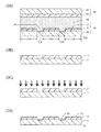
図2Aは、第1の実施例によるED素子101を示す断面図である。このED素子101は、主に、参考例によるED素子110の装飾電極が設けられた基板、つまり下側基板の構造を変更したものである。ED素子101は、主に、対向配置される下側および上側基板10,90と、下側および上側基板10,90に挟持される電解質層(電解液)50と、を備える。なお、図2Aでは、シール枠部材や電源装置等の図示を省略している。
FIG. 2A is a cross-sectional view showing the
上側基板90は、参考例によるED素子110のそれと同じ構造であり、支持基板91表面のほぼ全面に、表面が比較的平坦な透明電極92が形成された構造を有する。以降では、上側透明電極92をコモン電極92と呼び、上側基板90をコモン基板90と呼ぶことがある。
The
下側基板10は、支持基板11表面に、所定の平面形状にパターニングされた透明電極12が形成された構造を有する。支持基板11の表面は、一部、透明電極12から露出している。以降では、下側透明電極12をセグメント電極12と呼び、下側基板10をセグメント基板10と呼ぶことがある。
The
セグメント電極12の表面には、当該電極と一体的に形成された凸凹構造13が設けられている。セグメント電極12の表面は、少なくともコモン電極92の表面よりも粗くなっている。より具体的に、セグメント電極12の表面粗さ/凸凹構造13の算術平均粗さ(Ra)は、たとえば20nm以上である。なお、表面が比較的平坦なコモン電極92の表面粗さは、たとえば20nm以下である。
The surface of the
支持基板11の表面の、セグメント電極12から露出している領域11aにも、凸凹構造14が設けられている。支持基板11において、セグメント電極12から露出している領域11aの表面は、少なくともセグメント電極12により被覆されている領域11bの表面(セグメント電極12との接触界面)よりも粗くなっている。より具体的に、支持基板11の露出領域11aの表面粗さ/凸凹構造14の算術平均粗さ(Ra)は、たとえば20nm以上であり、被覆領域11bの表面粗さは、たとえば20nm以下である。
An
以下、ED素子101の製造方法について説明する。まず、図2B〜図2Dを参照して、セグメント基板10の作製方法について説明する。
Hereinafter, a method for manufacturing the
図2B〜図2Dは、セグメント基板10を製造する様子を示す断面図である。最初に、青板ガラスなどの支持基板11を準備する。支持基板11の平面形状は、たとえば一辺が15mm〜20mm程度の矩形状である。
2B to 2D are cross-sectional views showing how the
図2Bに示すように、支持基板11の表面全面に、スパッタリング法や真空蒸着法などにより、導電膜を形成する。当該導電膜は、たとえばITOなどにより形成され、厚みが約340nm程度の表面が平坦な膜である。続いて、フォトリソグラフィ法などを用いて、導電膜を所定の平面形状に成形(パターニング)して、セグメント電極12を形成する。このとき、支持基板11の表面は、一部、セグメント電極12から露出する。
As shown in FIG. 2B, a conductive film is formed on the entire surface of the
図2Cに示すように、支持基板11およびセグメント電極12の表面に、ブラスト処理を施す。たとえば、支持基板11ないしセグメント電極12から約50mm離れた位置から、平均粒径約3μmのアルミナ粒子を、空気圧約0.25MPaで吹き付ける。
As shown in FIG. 2C, the surface of the
図2Dに示すように、このようなブラスト処理を行うことで、セグメント電極12の表面に、多数の微細な凹部が形成される。すなわち、セグメント電極12の表面に、当該電極と一体的に形成される凸凹構造13が形成される。セグメント電極12の表面粗さは、たとえば、30nm程度である。なお、ブラスト処理は、支持基板11およびセグメント電極12を含む基板全面に施されるため、支持基板11の、セグメント電極12から露出する領域にも、凸凹構造14が形成される。
As shown in FIG. 2D, by performing such a blasting process, a large number of fine recesses are formed on the surface of the
以上により、下側基板10が完成する。再度、図2Aを参照して、ED素子101の製造方法について説明を続ける。
Thus, the
次に、上側基板90を作製する。下側基板10と同じ要領で、支持基板21(青板ガラス等)の表面全面に、コモン電極92(ITO等)を形成する。
Next, the
次に、下側または上側基板10,90のどちらかの基板、たとえば下側基板10に、粒径が数十μm〜数百μm、たとえば50μmであるギャップコントロール剤を散布する。ギャップコントロール剤の密度は、たとえば1〜3個/mm2程度である。なお、ギャップコントロール剤を散布するかわりに、柱状の突起体(リブ)を形成してもかまわない。また、ギャップコントロール剤は、上側基板90に散布してもかまわない。
Next, a gap control agent having a particle diameter of several tens of μm to several hundreds of μm, for example, 50 μm, is sprayed on either the lower or
続いて、下側または上側基板10,90のどちらかの基板、たとえば下側基板10に、シール枠部材40(図1A参照)を形成する。シール枠部材は、たとえば、矩形枠状の全体的平面形状を有し、紫外線硬化性樹脂により構成される。なお、シール枠部材は、熱硬化性樹脂により構成されていてもかまわない。
Subsequently, the seal frame member 40 (see FIG. 1A) is formed on either the lower or
次に、電解液(電解質層)50を準備する。そして、その電解液50を、ディスペンサなどを用いて、下側基板10のシール枠部材内側に滴下する。
Next, an electrolytic solution (electrolyte layer) 50 is prepared. Then, the
電解液50は、たとえば、ED材料(AgNO3等)、電解質(TBABr等)、メディエータ(CuCl2等)、溶媒(DMSO:dimethyl―sulfoxide 等)などにより構成される。なお、さらにゲル化用ポリマ(PVB:polyvinyl―butyral等)などを添加して、ゲル状(ゼリー状)にしてもよい。実施例においては、溶媒であるDMF(dimethyl―formamide)中に、ED材料としてAgNO3を350mM、支持電解質としてLiBrを700mM、メディエータとしてCuCl2を30mM添加したものを用いた。
The
ED材料は、AgNO3以外にも、たとえば銀を含むAgClO4やAgBrなどを用いることができる。ここで、ED材料とは、透明電極(ないし装飾電極)の表面において、酸化還元反応などにより、その一部が析出・堆積、または、消失する材料をいう。 In addition to AgNO 3 , for example, AgClO 4 containing silver, AgBr, or the like can be used as the ED material. Here, the ED material refers to a material in which a part thereof is deposited / deposited or disappears due to an oxidation-reduction reaction or the like on the surface of the transparent electrode (or decorative electrode).
支持電解質は、ED材料の酸化還元反応等を促進するものであれば限定されない。たとえば、リチウム塩(LiCl、LiBr、LiI、LiBF4、LiClO4等)、カリウム塩(KCl、KBr、KI等)、ナトリウム塩(NaCl、NaBr、NaI等)を好適に用いることができる。 The supporting electrolyte is not limited as long as it promotes the redox reaction or the like of the ED material. For example, lithium salts (LiCl, LiBr, LiI, LiBF 4 , LiClO 4 etc.), potassium salts (KCl, KBr, KI etc.), sodium salts (NaCl, NaBr, NaI etc.) can be suitably used.
メディエータは、銅を含むCuCl2以外にも、たとえば銅を含むCuSO4やCuBr2などを用いることができる。ここで、メディエータとは、銀よりも電気化学的に低いエネルギで酸化・還元する材料をいう。 As the mediator, in addition to CuCl 2 containing copper, for example, CuSO 4 containing Cu or CuBr 2 containing copper can be used. Here, the mediator refers to a material that is oxidized and reduced at an electrochemically lower energy than silver.
溶媒は、ED材料等を安定的に保持することができるものであれば限定されない。たとえば、水や炭酸プロピレン等の極性溶媒、極性のない有機溶媒、更にはイオン性液体、イオン導電性高分子、高分子電解質等を用いることができる。具体的には、DMSOの他、炭酸プロピレン、N,N−ジメチルホルムアミド、テトラヒドロフラン、アセトニトリル、ポリビニル硫酸、ポリスチレンスルホン酸、ポリアクリル酸等を好適に用いることができる。 A solvent will not be limited if it can hold | maintain ED material etc. stably. For example, polar solvents such as water and propylene carbonate, non-polar organic solvents, ionic liquids, ionic conductive polymers, polymer electrolytes, and the like can be used. Specifically, in addition to DMSO, propylene carbonate, N, N-dimethylformamide, tetrahydrofuran, acetonitrile, polyvinyl sulfate, polystyrene sulfonic acid, polyacrylic acid, and the like can be suitably used.
次に、透明電極12,92が相対するように、上側基板90を、電解液50を滴下した下側基板10に貼合する。なお、下側および上側基板10,20の貼合は、大気中、真空中ないし窒素雰囲気中で行うことができる。その後、シール枠部材に紫外線を照射して、シール枠部材を硬化させる。
Next, the
最後に、セグメント電極12およびコモン電極92に、電源装置(図1A参照)を接続する。電源装置は、たとえば所定の直流電圧を出力する。以上により、ED素子101が完成する。
Finally, a power supply device (see FIG. 1A) is connected to the
ED素子101は、参考例によるED素子110と同様に、定常時には、高光透過状態(透明状態)である。また、コモン電極92表面にED材料を堆積させれば、高光反射状態(鏡面状態)を実現する。
As in the case of the
コモン電極92を基準電位とし、セグメント電極12に負の直流電圧(−3.0V)を印加すると、セグメント電極12表面(凸凹構造13表面)にED材料(銀)が堆積する。ED材料が堆積した領域は、プラズモン吸収(ないし乱反射)により、光吸収状態(遮光/黒色状態)となる。すなわち、ED素子101は、セグメント電極12の平面形状に対応した黒色パターンを表示する。
When the
このように、微粒子が堆積してなる装飾電極に換えて、透明電極と一体化した凸凹構造とすることでも、ED素子は光吸収状態(遮光状態)を実現することができる。セグメント電極12表面の凸凹構造13は、当該電極と一体的に設けられているため、剥離等が生じ難いと推察される。このため、ED素子101において、電極表面の剥離等による性能低下が抑制されると考えられる。
In this way, the ED element can also realize a light absorption state (light-shielding state) by adopting a concave-convex structure integrated with the transparent electrode instead of the decorative electrode formed by depositing fine particles. Since the
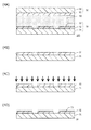
図3Aは、第2の実施例によるED素子102を示す断面図である。このED素子102は、主に、参考例によるED素子110ないし第1の実施例によるED素子101の、下側基板の構造を変更したものである。ED素子102は、主に、対向配置される下側基板(セグメント基板)20および上側基板(コモン基板)90と、セグメント基板20およびコモン基板90に挟持される電解質層(電解液)50と、を備える。
FIG. 3A is a cross-sectional view showing the
セグメント基板20は、支持基板21表面に、所定の平面形状にパターニングされたセグメント電極22が形成された構造を有する。支持基板21の表面は、一部、セグメント透明電極22から露出している。
The
セグメント電極22の表面には、当該電極と一体的に形成された凸凹構造23が設けられている。セグメント電極22の表面は、少なくともコモン電極92の表面よりも粗くなっている。より具体的に、セグメント電極22の表面粗さ/凸凹構造23の高低差は、たとえば20nm以上である。
The surface of the
支持基板21の表面全面にも、凸凹構造24が設けられている。第1の実施例と違って、セグメント電極22との接触界面も凸凹となっている。支持基板21の表面は、少なくともその裏面や対向する基板(上側支持基板91)の表面よりも粗くなっている。より具体的に、支持基板21の表面粗さ/凸凹構造24の高低差は、たとえば20nm以上である。
An
以下、ED素子102の製造方法について説明する。まず、図3B〜図3Dを参照して、セグメント基板20の作製方法について説明する。
Hereinafter, a method for manufacturing the
図3B〜図3Dは、セグメント基板20を製造する様子を示す断面図である。最初に、青板ガラスなどの支持基板21を準備する。
3B to 3D are cross-sectional views showing how the
図3Bに示すように、支持基板21の表面に、ブラスト処理を施す。たとえば、支持基板21から約50mm離れた位置から、平均粒径約3μmのアルミナ粒子を、空気圧約0.25MPaで吹き付ける。
As shown in FIG. 3B, the surface of the
図3Cに示すように、このようなブラスト処理を行うことで、支持基板21の表面に、多数の微細な凹部が形成される。すなわち、支持基板21の表面に、当該基板と一体的に形成される凸凹構造24が形成される。支持基板21の表面粗さは、たとえば19nm程度である。
As shown in FIG. 3C, by performing such a blasting process, a large number of fine recesses are formed on the surface of the
図3Dに示すように、支持基板21の表面全面に、パターニングされたセグメント電極22を形成する。セグメント電極22は、たとえばITO膜などからなり、スパッタリング法およびフォトリソグラフィ法を用いて作製することができる。
As shown in FIG. 3D, a
セグメント電極22は、表面が凸凹な支持基板21上に形成される。このため、セグメント電極22の表面も、支持基板21の表面と同程度に凸凹となる。すなわち、セグメント電極22は、当該電極と一体化した凸凹構造23を有する。
The
以上により、セグメント基板20が完成する。以降は、第1の実施例と同様に、コモン基板90を作製し、対向配置したセグメント基板20およびコモン基板90の間に、電解質層50を配置して、ED素子102を完成させる。
Thus, the
セグメント基板20がこのような構造であっても、電圧を印加してセグメント電極22表面(凸凹構造23表面)にED材料を堆積させれば、そのED材料が堆積した領域は、光吸収状態(遮光/黒色状態)となる。すなわち、ED素子102は、セグメント電極22の平面形状に対応した黒色パターンを表示する。なお、セグメント基板20を構成する支持基板21の表面全面に凸凹構造が設けられるため、セグメント基板側から光を入射させたとき、ED素子102の光反射率は、ED素子101と比べて、全面的に低減する。
Even if the
このように、ブラスト法などにより透明電極の表面を直接凸凹化することに換えて、支持基板の表面を凸凹化し、その上に透明電極を形成することによって、その透明電極の表面を凸凹化することでも、ED素子は光吸収状態(遮光状態)を実現することができる。セグメント電極22表面の凸凹構造23も、当該電極と一体的に設けられているため、剥離等が生じ難く、したがって、ED素子102において、電極表面の剥離等による性能低下が抑制されると考えられる。
In this way, instead of directly making the surface of the transparent electrode uneven by blasting or the like, the surface of the support substrate is made uneven, and the transparent electrode is formed thereon, thereby making the surface of the transparent electrode uneven. Even so, the ED element can realize a light absorption state (light shielding state). Since the
図4Aは、第3の実施例によるED素子103を示す断面図である。このED素子103は、主に、第1ないし第2の実施例によるED素子の、下側基板の構造を変更したものである。ED素子103は、主に、対向配置される下側基板(セグメント基板)30および上側基板(コモン基板)90と、セグメント基板30およびコモン基板90に挟持される電解質層(電解液)50と、を備える。
FIG. 4A is a cross-sectional view showing an
セグメント基板30は、支持基板31表面に、所定の平面形状にパターニングされたセグメント電極32が形成された構造を有する。支持基板31の表面は、一部、セグメント透明電極32から露出している。
The
セグメント電極32の表面には、当該電極と一体的に形成された凸凹構造33が設けられている。セグメント電極32の表面は、少なくともコモン電極92の表面よりも粗くなっている。より具体的に、セグメント電極32の表面粗さ/凸凹構造33の高低差は、たとえば20nm以上である。なお、支持基板33の表面は、全体的に比較的平坦である。
The surface of the
以下、ED素子103の製造方法について説明する。まず、図4B〜図4Dを参照して、セグメント基板30の作製方法について説明する。
Hereinafter, a method for manufacturing the
図4B〜図4Dは、セグメント基板20を製造する様子を示す断面図である。最初に、青板ガラスなどの支持基板31を準備する。
4B to 4D are cross-sectional views showing how the
図4Bに示すように、支持基板31の表面全面に、スパッタリング法や真空蒸着法などにより、表面が平坦な導電膜を形成する。当該導電膜は、たとえばITOなどにより形成される。続いて、フォトリソグラフィ法などを用いて、導電膜を所定の平面形状に成形(パターニング)して、セグメント電極32を形成する。
As shown in FIG. 4B, a conductive film having a flat surface is formed on the entire surface of the
図4Cに示すように、主にセグメント電極32に、エッチング処理を施す。エッチャントとして、たとえばシュウ酸の濃度が5%以下の水溶液を用いる。電極32付きの基板31を、たとえば室温のエッチャントに900秒間浸漬する。
As shown in FIG. 4C, the
図4Dに示すように、このようなエッチング処理を行うことで、セグメント電極32の表面に、多数の微細な凹部が形成される。すなわち、セグメント電極32の表面に、当該電極と一体的に形成される凸凹構造33が形成される。なお、ここで用いたエッチャントは、電極(ITO)に対しては作用するが、基板(主成分がSiO2のガラス)に対しては作用しないため、支持基板31の、セグメント電極32から露出する領域には、凸凹構造は形成されない。
As shown in FIG. 4D, by performing such an etching process, a large number of fine recesses are formed on the surface of the
以上により、セグメント基板30が完成する。以降は、第1の実施例と同様に、コモン基板90を作製し、対向配置したセグメント基板30およびコモン基板90の間に、電解質層50を配置して、ED素子103を完成させる。
Thus, the
セグメント基板30がこのような構造であっても、電圧を印加してセグメント電極32表面(凸凹構造33表面)にED材料を堆積させれば、そのED材料が堆積した領域は、光吸収状態(遮光/黒色状態)となる。セグメント電極32表面の凸凹構造33も、当該電極と一体的に設けられているため、剥離等が生じ難く、したがって、ED素子103において、電極表面の剥離等による性能低下が抑制されると考えられる。
Even if the
以上、本発明を実施するための形態について説明したが、本発明はこれらに制限されるものではない。たとえば、電極表面に設けられる凸凹構造は、セグメント電極側ではなくコモン電極側に設けてもよい。または、セグメント電極およびコモン電極の両方に設けてもかまわない。その他、種々の変更、改良、組み合わせ等が可能なことは当業者に自明であろう。 As mentioned above, although the form for implementing this invention was demonstrated, this invention is not restrict | limited to these. For example, the uneven structure provided on the electrode surface may be provided on the common electrode side instead of the segment electrode side. Alternatively, both the segment electrode and the common electrode may be provided. It will be apparent to those skilled in the art that other various modifications, improvements, combinations, and the like can be made.
10…下側基板(第1実施例)、11…下側支持基板、12…下側透明電極、13,14…凸凹構造、20…下側基板(第2実施例)、21…上側支持基板、22…上側透明電極、23,24…凸凹構造、30…下側基板(第3実施例)、31…下側支持基板、32…下側透明電極、33…凸凹構造、40…シール枠部材、50電解質層(電解液)、60…電源装置、80…下側基板(参考例)、81…下側支持基板、82…下側透明電極、83…装飾電極、90…上側基板、91…上側支持基板、92…上側透明電極、101…エレクトロデポジション素子(第1実施例)、102…エレクトロデポジション素子(第2実施例)、103…エレクトロデポジション素子(第3実施例)、110…エレクトロデポジション素子(参考例)。
DESCRIPTION OF
Claims (5)
前記第1の基板の、前記第2の基板との対向面に配置される第1の電極であって、表面に一体的に形成された凸凹構造を含む第1の電極と、
前記第2の基板の、前記第1の基板との対向面に配置される第2の電極と、
前記第1および第2の基板の間隙に、銀を含むエレクトロデポジション材料を含有する電解質層と、
を有する光学素子。 First and second substrates disposed opposite to each other;
A first electrode disposed on a surface of the first substrate facing the second substrate, the first electrode including an uneven structure formed integrally on the surface;
A second electrode disposed on a surface of the second substrate facing the first substrate;
An electrolyte layer containing an electrodeposition material containing silver in the gap between the first and second substrates;
An optical element.
前記第1の基板において、前記第1の電極から露出している部分の表面は、相対的に凸凹であり、前記第1の電極との接触界面は、相対的に平坦である請求項1記載の光学素子。 The first electrode is disposed so as to expose a part of the surface of the first substrate,
The surface of the part exposed from the said 1st electrode in the said 1st board | substrate is relatively uneven, The contact interface with the said 1st electrode is relatively flat. Optical elements.
前記第1の基板において、前記第1の電極から露出している部分の表面は、凸凹であり、前記第1の電極との接触界面も、凸凹である請求項1記載の光学素子。 The first electrode is disposed so as to expose a part of the surface of the first substrate,
2. The optical element according to claim 1, wherein a surface of a portion of the first substrate exposed from the first electrode is uneven, and a contact interface with the first electrode is also uneven.
前記第1の電極に、ブラスト法またはエッチング法により、凸凹構造を形成する工程と、
第2の基板に、第2の電極を形成する工程と、
銀を含むエレクトロデポジション材料を含有する電解質層を挟んで、前記第1の基板と前記第2の基板とを、前記第1の電極と前記第2の電極が対向するように重ね合せる工程と、
を有する光学素子の製造方法。 Forming a first electrode having a flat surface on a first substrate;
Forming a concavo-convex structure on the first electrode by blasting or etching;
Forming a second electrode on a second substrate;
Sandwiching an electrolyte layer containing an electrodeposition material containing silver, and stacking the first substrate and the second substrate such that the first electrode and the second electrode face each other; ,
The manufacturing method of the optical element which has these.
前記第1の基板上に第1の電極を形成して、該第1の電極の表面に該第1の基板の凸凹構造を反映させる工程と、
第2の基板に、第2の電極を形成する工程と、
銀を含むエレクトロデポジション材料を含有する電解質層を挟んで、前記第1の基板と前記第2の基板とを、前記第1の電極と前記第2の電極が対向するように重ね合せる工程と、
を有する光学素子の製造方法。 Forming an uneven structure on the first substrate;
Forming a first electrode on the first substrate and reflecting the uneven structure of the first substrate on the surface of the first electrode;
Forming a second electrode on a second substrate;
Sandwiching an electrolyte layer containing an electrodeposition material containing silver, and stacking the first substrate and the second substrate such that the first electrode and the second electrode face each other; ,
The manufacturing method of the optical element which has these.
Priority Applications (1)
| Application Number | Priority Date | Filing Date | Title |
|---|---|---|---|
| JP2016080324A JP6892738B2 (en) | 2016-04-13 | 2016-04-13 | Optical element and manufacturing method of optical element |
Applications Claiming Priority (1)
| Application Number | Priority Date | Filing Date | Title |
|---|---|---|---|
| JP2016080324A JP6892738B2 (en) | 2016-04-13 | 2016-04-13 | Optical element and manufacturing method of optical element |
Publications (3)
| Publication Number | Publication Date |
|---|---|
| JP2017191202A true JP2017191202A (en) | 2017-10-19 |
| JP2017191202A5 JP2017191202A5 (en) | 2019-06-06 |
| JP6892738B2 JP6892738B2 (en) | 2021-06-23 |
Family
ID=60085899
Family Applications (1)
| Application Number | Title | Priority Date | Filing Date |
|---|---|---|---|
| JP2016080324A Active JP6892738B2 (en) | 2016-04-13 | 2016-04-13 | Optical element and manufacturing method of optical element |
Country Status (1)
| Country | Link |
|---|---|
| JP (1) | JP6892738B2 (en) |
Cited By (2)
| Publication number | Priority date | Publication date | Assignee | Title |
|---|---|---|---|---|
| WO2019064859A1 (en) | 2017-09-29 | 2019-04-04 | アルプスアルパイン株式会社 | Operation input device and door handle |
| CN111123610A (en) * | 2018-11-01 | 2020-05-08 | 苏州苏大维格科技集团股份有限公司 | Electrochromic display panel and electronic paper |
Citations (6)
| Publication number | Priority date | Publication date | Assignee | Title |
|---|---|---|---|---|
| JP2005189386A (en) * | 2003-12-25 | 2005-07-14 | Sony Corp | Electrochemical light control device and method for manufacturing the same |
| KR20080051280A (en) * | 2006-12-05 | 2008-06-11 | 주식회사 엘지화학 | Electrochromic device electrode and electrochromic device having same |
| JP2010048867A (en) * | 2008-08-19 | 2010-03-04 | Canon Inc | Reflection type display apparatus |
| US20110181811A1 (en) * | 2008-07-07 | 2011-07-28 | Fredericus Johannes Touwslager | display structure with a roughened sub-electrode layer |
| JP2015082081A (en) * | 2013-10-24 | 2015-04-27 | スタンレー電気株式会社 | Optical device, imaging device and driving method of optical element |
| KR20150088565A (en) * | 2014-01-24 | 2015-08-03 | 한국전자통신연구원 | Electrode of a wrinkle structure, display device having the same and method of fabricating the same |
-
2016
- 2016-04-13 JP JP2016080324A patent/JP6892738B2/en active Active
Patent Citations (6)
| Publication number | Priority date | Publication date | Assignee | Title |
|---|---|---|---|---|
| JP2005189386A (en) * | 2003-12-25 | 2005-07-14 | Sony Corp | Electrochemical light control device and method for manufacturing the same |
| KR20080051280A (en) * | 2006-12-05 | 2008-06-11 | 주식회사 엘지화학 | Electrochromic device electrode and electrochromic device having same |
| US20110181811A1 (en) * | 2008-07-07 | 2011-07-28 | Fredericus Johannes Touwslager | display structure with a roughened sub-electrode layer |
| JP2010048867A (en) * | 2008-08-19 | 2010-03-04 | Canon Inc | Reflection type display apparatus |
| JP2015082081A (en) * | 2013-10-24 | 2015-04-27 | スタンレー電気株式会社 | Optical device, imaging device and driving method of optical element |
| KR20150088565A (en) * | 2014-01-24 | 2015-08-03 | 한국전자통신연구원 | Electrode of a wrinkle structure, display device having the same and method of fabricating the same |
Cited By (2)
| Publication number | Priority date | Publication date | Assignee | Title |
|---|---|---|---|---|
| WO2019064859A1 (en) | 2017-09-29 | 2019-04-04 | アルプスアルパイン株式会社 | Operation input device and door handle |
| CN111123610A (en) * | 2018-11-01 | 2020-05-08 | 苏州苏大维格科技集团股份有限公司 | Electrochromic display panel and electronic paper |
Also Published As
| Publication number | Publication date |
|---|---|
| JP6892738B2 (en) | 2021-06-23 |
Similar Documents
| Publication | Publication Date | Title |
|---|---|---|
| JP6278384B2 (en) | OPTICAL DEVICE, IMAGING DEVICE, AND OPTICAL ELEMENT DRIVE METHOD | |
| CN105190421B (en) | Electrodeposited components | |
| JP6138417B2 (en) | Electrochromic display element | |
| WO2011021470A1 (en) | Method for manufacturing a transparent conductive substrate, transparent conductive substrate, and electrochemical display element | |
| CN109283704A (en) | reversible electrochemical mirror | |
| JP6461643B2 (en) | Optical device | |
| JP2010002573A (en) | Method for changing reflectivity reversibly, element therefor, method of manufacturing element, and transmittance variable element and reflectivity variable mirror | |
| CN114730116A (en) | Method of manufacturing flexible electrochromic device | |
| JP2019066619A (en) | Electrochemical optical device | |
| JP6892738B2 (en) | Optical element and manufacturing method of optical element | |
| JP6763523B2 (en) | How to drive the mirror device and electrodeposition element | |
| JP6358611B2 (en) | Optical device, vehicular lamp, and optical element driving method | |
| JP2011164256A (en) | Electrochemical display element | |
| WO2009157244A1 (en) | Electrically conductive transparent substrate, method for production of electrically conductive transparent substrate, and electrochemical display element | |
| JP2017191201A (en) | Display device | |
| JP6314035B2 (en) | Illumination device and photographing auxiliary light source device | |
| JP7492384B2 (en) | Electrochemical Equipment | |
| WO2018021302A1 (en) | Electrochemical device | |
| CN209281120U (en) | A kind of electrochromic device and device | |
| JP6496515B2 (en) | Optical apparatus and optical element driving method | |
| CN114127627B (en) | Electrochemical device | |
| JP2011141416A (en) | Method of manufacturing conductive color filter substrate, conductive color filter substrate, reflective display element, and electrochemical display element | |
| JP6430154B2 (en) | Mirror device for imaging unit | |
| JP6355945B2 (en) | Lighting device | |
| JP2025012239A (en) | Electrochromic device and display device |
Legal Events
| Date | Code | Title | Description |
|---|---|---|---|
| A521 | Request for written amendment filed |
Free format text: JAPANESE INTERMEDIATE CODE: A523 Effective date: 20190410 |
|
| A621 | Written request for application examination |
Free format text: JAPANESE INTERMEDIATE CODE: A621 Effective date: 20190410 |
|
| A977 | Report on retrieval |
Free format text: JAPANESE INTERMEDIATE CODE: A971007 Effective date: 20200221 |
|
| A131 | Notification of reasons for refusal |
Free format text: JAPANESE INTERMEDIATE CODE: A131 Effective date: 20200303 |
|
| A521 | Request for written amendment filed |
Free format text: JAPANESE INTERMEDIATE CODE: A523 Effective date: 20200507 |
|
| A131 | Notification of reasons for refusal |
Free format text: JAPANESE INTERMEDIATE CODE: A131 Effective date: 20201027 |
|
| A521 | Request for written amendment filed |
Free format text: JAPANESE INTERMEDIATE CODE: A523 Effective date: 20201225 |
|
| TRDD | Decision of grant or rejection written | ||
| A01 | Written decision to grant a patent or to grant a registration (utility model) |
Free format text: JAPANESE INTERMEDIATE CODE: A01 Effective date: 20210511 |
|
| A61 | First payment of annual fees (during grant procedure) |
Free format text: JAPANESE INTERMEDIATE CODE: A61 Effective date: 20210528 |
|
| R150 | Certificate of patent or registration of utility model |
Ref document number: 6892738 Country of ref document: JP Free format text: JAPANESE INTERMEDIATE CODE: R150 |
|
| R250 | Receipt of annual fees |
Free format text: JAPANESE INTERMEDIATE CODE: R250 |
|
| R250 | Receipt of annual fees |
Free format text: JAPANESE INTERMEDIATE CODE: R250 |