JP2017174765A - Electronic switch device and electronic switch system - Google Patents
Electronic switch device and electronic switch system Download PDFInfo
- Publication number
- JP2017174765A JP2017174765A JP2016062510A JP2016062510A JP2017174765A JP 2017174765 A JP2017174765 A JP 2017174765A JP 2016062510 A JP2016062510 A JP 2016062510A JP 2016062510 A JP2016062510 A JP 2016062510A JP 2017174765 A JP2017174765 A JP 2017174765A
- Authority
- JP
- Japan
- Prior art keywords
- unit
- power supply
- switch
- electronic switch
- power
- Prior art date
- Legal status (The legal status is an assumption and is not a legal conclusion. Google has not performed a legal analysis and makes no representation as to the accuracy of the status listed.)
- Granted
Links
- 239000003990 capacitor Substances 0.000 claims description 29
- 230000005669 field effect Effects 0.000 claims description 3
- 238000012544 monitoring process Methods 0.000 description 25
- 230000002457 bidirectional effect Effects 0.000 description 9
- 238000001514 detection method Methods 0.000 description 9
- 230000006870 function Effects 0.000 description 8
- 238000012986 modification Methods 0.000 description 7
- 230000004048 modification Effects 0.000 description 7
- 238000010248 power generation Methods 0.000 description 7
- 238000010586 diagram Methods 0.000 description 5
- 239000004065 semiconductor Substances 0.000 description 5
- 230000000052 comparative effect Effects 0.000 description 4
- 229910002601 GaN Inorganic materials 0.000 description 2
- JMASRVWKEDWRBT-UHFFFAOYSA-N Gallium nitride Chemical compound [Ga]#N JMASRVWKEDWRBT-UHFFFAOYSA-N 0.000 description 2
- 230000007257 malfunction Effects 0.000 description 2
- 238000004804 winding Methods 0.000 description 2
- 230000015556 catabolic process Effects 0.000 description 1
- 238000004891 communication Methods 0.000 description 1
- 239000004020 conductor Substances 0.000 description 1
- 238000013461 design Methods 0.000 description 1
- 230000009977 dual effect Effects 0.000 description 1
- 239000000463 material Substances 0.000 description 1
- 238000012545 processing Methods 0.000 description 1
- 238000012546 transfer Methods 0.000 description 1
- 238000009423 ventilation Methods 0.000 description 1
Images


Classifications
-
- H—ELECTRICITY
- H05—ELECTRIC TECHNIQUES NOT OTHERWISE PROVIDED FOR
- H05B—ELECTRIC HEATING; ELECTRIC LIGHT SOURCES NOT OTHERWISE PROVIDED FOR; CIRCUIT ARRANGEMENTS FOR ELECTRIC LIGHT SOURCES, IN GENERAL
- H05B47/00—Circuit arrangements for operating light sources in general, i.e. where the type of light source is not relevant
- H05B47/10—Controlling the light source
-
- G—PHYSICS
- G01—MEASURING; TESTING
- G01V—GEOPHYSICS; GRAVITATIONAL MEASUREMENTS; DETECTING MASSES OR OBJECTS; TAGS
- G01V8/00—Prospecting or detecting by optical means
- G01V8/10—Detecting, e.g. by using light barriers
- G01V8/12—Detecting, e.g. by using light barriers using one transmitter and one receiver
-
- G—PHYSICS
- G05—CONTROLLING; REGULATING
- G05F—SYSTEMS FOR REGULATING ELECTRIC OR MAGNETIC VARIABLES
- G05F3/00—Non-retroactive systems for regulating electric variables by using an uncontrolled element, or an uncontrolled combination of elements, such element or such combination having self-regulating properties
- G05F3/02—Regulating voltage or current
- G05F3/08—Regulating voltage or current wherein the variable is dc
- G05F3/10—Regulating voltage or current wherein the variable is dc using uncontrolled devices with non-linear characteristics
- G05F3/16—Regulating voltage or current wherein the variable is dc using uncontrolled devices with non-linear characteristics being semiconductor devices
- G05F3/18—Regulating voltage or current wherein the variable is dc using uncontrolled devices with non-linear characteristics being semiconductor devices using Zener diodes
Landscapes
- Physics & Mathematics (AREA)
- General Physics & Mathematics (AREA)
- Life Sciences & Earth Sciences (AREA)
- Geophysics (AREA)
- Engineering & Computer Science (AREA)
- General Life Sciences & Earth Sciences (AREA)
- Electromagnetism (AREA)
- Automation & Control Theory (AREA)
- Radar, Positioning & Navigation (AREA)
- Nonlinear Science (AREA)
- Circuit Arrangement For Electric Light Sources In General (AREA)
- Geophysics And Detection Of Objects (AREA)
- Control Of Electrical Variables (AREA)
- Continuous-Control Power Sources That Use Transistors (AREA)
- Rectifiers (AREA)
Abstract
Description
本発明は、一般に電子スイッチ装置及び電子スイッチシステムに関し、より詳細には、交流電源と負荷との間に電気的に接続されるスイッチ部を備える電子スイッチ装置及び電子スイッチシステムに関する。 The present invention generally relates to an electronic switch device and an electronic switch system, and more particularly to an electronic switch device and an electronic switch system including a switch unit that is electrically connected between an AC power supply and a load.
従来、人体から放射される熱線を検出して、負荷をオン/オフさせる電子スイッチ装置(熱線センサ付自動スイッチ)が知られている(例えば、特許文献1参照)。特許文献1に記載の電子スイッチ装置は、接続端子間に、カレントトランスの1次巻線と、全波整流器と、負荷への電源供給をオン/オフ制御する双方向サイリスタを有する負荷制御回路とが直列に接続されている。
2. Description of the Related Art Conventionally, an electronic switch device (automatic switch with a heat ray sensor) that detects a heat ray radiated from a human body and turns on / off a load is known (for example, see Patent Document 1). The electronic switch device described in
また、特許文献1に記載の電子スイッチ装置では、全波整流器の直流出力端子間には、電源回路が接続される。電源回路は、制御用IC(Integrated Circuit)用の制御電源(動作電源)を生成する定電圧回路に、負荷の非通電時に電源供給する。また、負荷の通電時には、カレントトランスの2次巻線に流れる電流により、補助電源回路が定電圧回路に電源供給する。
Moreover, in the electronic switch device described in
特許文献1に記載の電子スイッチ装置は、負荷の通電時に制御電源を確保するためにカレントトランスが必要であるから、小型化が困難であるという問題がある。
The electronic switch device described in
本発明は上記事由に鑑みてなされており、小型化が可能な電子スイッチ装置及び電子スイッチシステムを提供することを目的とする。 The present invention has been made in view of the above-described reasons, and an object thereof is to provide an electronic switch device and an electronic switch system that can be miniaturized.
本発明の一態様に係る電子スイッチ装置は、電子スイッチ装置は、スイッチ部と、電源部と、制御部と、給電回路と、を備えている。前記スイッチ部は、交流電源と負荷との間に電気的に接続され、前記交流電源と前記負荷との間の導通/非導通を切り替える。前記電源部は、前記スイッチ部の両端間に電気的に接続され、前記交流電源からの供給電力により制御電源を生成する。前記制御部は、前記電源部から前記制御電源の供給を受けて動作し、前記スイッチ部を制御する。前記給電回路は、前記スイッチ部の両端間に電気的に接続され、前記スイッチ部と前記電源部との間における前記供給電力の単一の経路となる。前記給電回路は、前記スイッチ部の前記両端間の電圧の大きさが所定値以上になれば前記電源部に前記供給電力を供給するように構成されている。 An electronic switch device according to one embodiment of the present invention includes a switch unit, a power supply unit, a control unit, and a power feeding circuit. The switch unit is electrically connected between an AC power source and a load, and switches between conduction and non-conduction between the AC power source and the load. The power supply unit is electrically connected between both ends of the switch unit, and generates a control power supply by power supplied from the AC power supply. The control unit operates by receiving the control power from the power supply unit and controls the switch unit. The power feeding circuit is electrically connected between both ends of the switch unit, and serves as a single path for the supplied power between the switch unit and the power supply unit. The power supply circuit is configured to supply the supply power to the power supply unit when the magnitude of the voltage between the both ends of the switch unit exceeds a predetermined value.
本発明の一態様に係る電子スイッチシステムは、前記電子スイッチ装置を複数備え、前記複数の電子スイッチ装置が備える複数のスイッチ部は、交流電源と負荷との間に電気的に並列に接続される。 An electronic switch system according to an aspect of the present invention includes a plurality of the electronic switch devices, and the plurality of switch units included in the plurality of electronic switch devices are electrically connected in parallel between an AC power supply and a load. .
本発明は、小型化が可能になるという利点がある。 The present invention has an advantage that downsizing is possible.
(実施形態1)
(1)概要
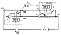
実施形態1に係る電子スイッチ装置1A,1Bは、図2に示すように、交流電源11と負荷12との間に電気的に接続され、交流電源11から負荷12への通電状態を切り替える配線器具である。電子スイッチ装置1A,1Bは、例えば住宅の壁等に取り付けられる。交流電源11は、例えば、単相100〔V〕、60〔Hz〕の商用電源である。負荷12は、例えば、LED(Light Emitting Diode)を有する光源と、光源を点灯させる点灯回路とを備える照明装置である。この負荷12では、交流電源11からの電力供給時に光源が点灯する。
(Embodiment 1)
(1) Outline As shown in FIG. 2, the
図2に示す例では、2つの電子スイッチ装置1A,1Bにて、電子スイッチシステム10が構成されている。つまり、電子スイッチシステム10は、複数(ここでは2つ)の電子スイッチ装置1A,1Bを備えている。2つの電子スイッチ装置1A,1Bは、互いに共通の構成を採用している。以下、2つの電子スイッチ装置1A,1Bをとくに区別しない場合には、2つの電子スイッチ装置1A,1Bの各々を「電子スイッチ装置1」という。
In the example shown in FIG. 2, the
電子スイッチ装置1は、例えば、双方向サイリスタ及びトランジスタ等の半導体スイッチからなるスイッチ部Q1を備えている。電子スイッチ装置1は、スイッチ部Q1を電子的に制御することにより、交流電源11と負荷12との間の導通/非導通を電子的に切り替える。
The
本実施形態では、電子スイッチ装置1は、3本の配線を接続可能な、いわゆる三路スイッチである。電子スイッチ装置1は、3つの接続端子101,102,103を備えている。そのため、2つの電子スイッチ装置1A,1Bを組み合わせた電子スイッチシステム10では、負荷12への通電状態を、例えば、建物における階段の上階部分と下階部分との2箇所で切り替えることが可能である。
In this embodiment, the
図2の例では、電子スイッチ装置1A(以下、「第1電子スイッチ装置1A」ともいう)の接続端子101は、負荷12に接続されている。電子スイッチ装置1B(以下、「第2電子スイッチ装置1B」ともいう)の接続端子101は、交流電源11に接続されている。また、電子スイッチ装置1Aの接続端子102は、電子スイッチ装置1Bの接続端子103に接続されている。電子スイッチ装置1Aの接続端子103は、電子スイッチ装置1Bの接続端子102に接続されている。各電子スイッチ装置1において、接続端子101と接続端子102とは電子スイッチ装置1の内部で接続されている。
In the example of FIG. 2, the
さらに、各電子スイッチ装置1において、スイッチ部Q1は、接続端子101と接続端子103との間に接続されている。したがって、各電子スイッチ装置1において、スイッチ部Q1が導通(オン)した状態では、接続端子101及び接続端子102と、接続端子103との間がスイッチ部Q1を介して導通する。また、各電子スイッチ装置1において、スイッチ部Q1が非導通(オフ)の状態では、接続端子101及び接続端子102と、接続端子103との間が非導通となる。
Further, in each
すなわち、複数(ここでは2つ)の電子スイッチ装置1A,1Bがそれぞれ備える複数のスイッチ部Q1は、交流電源11と負荷12との間に電気的に並列に接続される。そのため、電子スイッチシステム10では、2つの電子スイッチ装置1A,1Bのいずれかのスイッチ部Q1が導通していれば、交流電源11と負荷12との間が導通し、2つの電子スイッチ装置1A,1Bを介して、交流電源11から負荷12に電力供給される。したがって、電子スイッチシステム10では、電子スイッチ装置1Aのスイッチ部Q1、及び電子スイッチ装置1Bのスイッチ部Q1の両方において、負荷12への通電状態を切り替えることが可能である。
That is, the plurality of switch units Q1 provided in each of the plurality (two in this case) of
(2)詳細
(2.1)電子スイッチ装置の全体構成
以下、本実施形態の電子スイッチ装置の構成について、図1及び図2を参照して説明する。
(2) Details (2.1) Overall Configuration of Electronic Switch Device Hereinafter, the configuration of the electronic switch device of the present embodiment will be described with reference to FIGS. 1 and 2.
電子スイッチ装置1は、図2に示すように、スイッチ部Q1及び3つの接続端子101,102,103に加えて、整流器2及び回路部3を備えている。これらのスイッチ部Q1、3つの接続端子101,102,103、整流器2及び回路部3は、1つの筐体に収納されており、筐体が壁等に固定されることで、電子スイッチ装置1は壁等に取り付けられる。
As shown in FIG. 2, the
スイッチ部Q1は、交流電源11と負荷12との間に電気的に接続され、交流電源11と負荷12との間の導通/非導通を切り替える。本実施形態では、スイッチ部Q1は、3端子の双方向サイリスタ(トライアック)にて構成されている。スイッチ部Q1は、接続端子101と接続端子103との間に電気的に接続されており、接続端子101と接続端子103との間における双方向の電流の通過/遮断を切り替える。スイッチ部Q1の制御端子(双方向サイリスタのゲート端子)は、回路部3に電気的に接続されている。これにより、スイッチ部Q1は、後述する制御部5にて制御される。図1及び図2等では、スイッチ部Q1を、接点を有するメカニカルスイッチと同様の回路記号で表記している。
The switch unit Q1 is electrically connected between the
3つの接続端子101,102,103の各々は、配線が電気的かつ機械的に接続される部品である。第1の接続端子101と第3の接続端子103との間には、上述したようにスイッチ部Q1が接続されている。第2の接続端子102は、第1の接続端子101の送り端子であり、第1の接続端子101と電気的に接続されている。
Each of the three
整流器2は、ダイオードブリッジからなる。整流器2は、スイッチ部Q1の両端間に印加される電圧(以下、「スイッチ間電圧Vsw」ともいう)を、全波整流して、回路部3に出力する。そのため、回路部3は、整流器2の直流出力端子間に接続されている。回路部3は、整流器2から入力される、全波整流後の電力を用いて、例えばスイッチ部Q1の制御及びセンサ部31の駆動等に必要な「制御電源」を生成する。
The
以下では、2つの電子スイッチ装置1A,1Bのいずれのスイッチ部Q1も非導通の状態で、スイッチ部Q1には交流電源11から交流電圧Vacが印加されることと仮定する。つまり、2つの電子スイッチ装置1A,1Bがいずれもオフ状態であれば、スイッチ間電圧Vswは交流電源11からの交流電圧Vacと等しくなる。
In the following, it is assumed that the switch part Q1 of the two
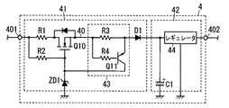
次に、回路部3の詳細について、図1を参照して説明する。回路部3は、電源生成ブロック4と、制御部5と、センサ部31と、電圧監視部32とを備えている。
Next, details of the
電源生成ブロック4は、給電回路41と、電源部42とを有している。電源部42は、スイッチ部Q1の両端間に電気的に接続されている。電源部42は、交流電源11からの供給電力により制御電源を生成するように構成されている。給電回路41は、スイッチ部Q1の両端間に電気的に接続されている。給電回路41は、スイッチ部Q1と電源部42との間における、交流電源11から電源部42への供給電力の単一の経路となる。ここでいう「単一」とは、ただ一つであることを意味する。つまり、給電回路41は、スイッチ部Q1と電源部42との間に、電源部42への供給電力の経路として、唯一の経路を形成する。言い換えれば、交流電源11から電源部42への供給電力の経路は、スイッチ部Q1と電源部42との間に一つだけ存在するのであって、給電回路41以外には、電源部42への供給電力の経路は存在しない。
The power
すなわち、給電回路41と電源部42とは、整流器2の直流出力端子間において、電気的に直列に接続されている。電源入力端子401は、給電回路41の入力端子に相当し、整流器2の正極の直流出力端子に電気的に接続される。そのため、スイッチ部Q1がオフ状態にある場合、電源入力端子401とグランド(基準電位点)との間には、全波整流されたスイッチ間電圧Vsw、つまり整流器2から出力される脈流電圧が印加されることになる。電源出力端子402は、電源部42の出力端子に相当し、制御部5に電気的に接続される。これにより、電源部42が制御電源を生成するときには、電源部42への供給電力は、必ず給電回路41を介して電源部42に供給されることになる。給電回路41は、スイッチ間電圧Vswの大きさ(絶対値)が所定値以上になれば電源部42に供給電力を供給するように構成されている。給電回路41は、例えば、入力電圧(スイッチ間電圧Vsw)を降圧して電源部42に出力するドロッパ回路である。電源生成ブロック4の具体的な構成については、「(2.2)電源生成ブロックの構成」の欄で説明する。
That is, the
本実施形態における「電源入力端子」等の「端子」は、電線等を接続するための部品(端子)として実体を有しなくてもよく、例えば、電子部品のリードや、回路基板に含まれる導体の一部であってもよい。 The “terminal” such as “power input terminal” in the present embodiment may not have an entity as a component (terminal) for connecting an electric wire or the like, and is included in, for example, a lead of an electronic component or a circuit board. It may be a part of a conductor.
制御部5は、電源生成ブロック4から、制御電源の供給を受けて動作する。制御部5は、スイッチ部Q1を制御する機能を備えている。具体的には、制御部5は、センサ部31の検知結果に基づいて、スイッチ部Q1の制御端子(双方向サイリスタのゲート端子)に制御信号を出力することにより、スイッチ部Q1の導通/非導通を切り替えるように、スイッチ部Q1を制御する。さらに、制御部5は、スイッチ部Q1をオン状態とする場合には、電圧監視部32から出力される監視信号に基づいて、制御信号を出力するタイミングを決定する。制御部5にはスイッチ部Q1を駆動するための駆動回路が含まれており、制御部5は直接的にスイッチ部Q1を制御する。
The
制御部5は、例えば、マイクロコンピュータを主構成として備えている。マイクロコンピュータは、マイクロコンピュータのメモリに記録されているプログラムをCPU(Central Processing Unit)で実行することにより、制御部5としての機能を実現する。プログラムは、予めマイコンのメモリに記録されていてもよいし、メモリカードのような記録媒体に記録されて提供されたり、電気通信回線を通して提供されたりしてもよい。言い換えれば、上記プログラムは、マイクロコンピュータを、制御部5として機能させるためのプログラムである。
The
センサ部31は、検知エリアに人が存在するか否かを検知する。センサ部31は、例えば、焦電素子を含んでおり、人体から放出される赤外線を検出することによって、検知エリアに人が存在するか否かを判断する。センサ部31は、検知エリアに人が存在することを検知すると、スイッチ部Q1をオン状態とするためのオン制御指示を、制御部5に出力する。
The
電圧監視部32は、スイッチ間電圧Vswの大きさを監視(検出)するように構成されている。本実施形態では、電圧監視部32は、整流器2の直流出力端子間に電気的に接続されており、全波整流後のスイッチ間電圧Vswの大きさを監視する。電圧監視部32は、スイッチ間電圧Vswの大きさ(絶対値)と基準値とを比較し、比較結果を表す監視信号を制御部5に出力する。
The
制御部5は、センサ部31からオン制御指示を受けると、電圧監視部32からの監視信号に基づいて、スイッチ部Q1に制御信号を出力する。具体的には、制御部5は、電圧監視部32からの監視信号に基づいて、スイッチ間電圧Vswの大きさ(絶対値)が基準値以上になった際に、スイッチ部Q1を導通させる。スイッチ部Q1は、上述したように双方向サイリスタからなるので、制御信号が入力されると導通し、交流電源11からの交流電圧Vacのゼロクロス点(0〔V〕)付近で非導通となる。厳密には、スイッチ部Q1が導通後、スイッチ部Q1を流れる電流が0〔A〕になるとスイッチ部Q1が非導通となるので、負荷12の種類によっては、交流電圧Vacのゼロクロス点よりも早いタイミングでスイッチ部Q1が非導通となることもある。そこで、制御部5は、交流電圧Vacの半周期ごとに制御信号を出力することにより、スイッチ部Q1を導通する。つまり、ここでいうスイッチ部Q1のオン状態とは、スイッチ部Q1が連続的に導通している状態だけではなく、スイッチ部Q1が間欠的に導通している状態を含む。また、制御部5は、スイッチ部Q1をオフ状態とする場合、スイッチ部Q1に制御信号を出力しないことにより、スイッチ部Q1を非導通に維持する。
When receiving the ON control instruction from the
(2.2)電源生成ブロック
次に、電源生成ブロック4の詳細について、図3を参照して説明する。
(2.2) Power Generation Block Next, details of the
給電回路41は、ツェナダイオードZD1と、能動素子Q10と、第1の抵抗R1と、第2の抵抗R2と、ダイオードD1と、電流制限部43とを有している。電源部42は、コンデンサC1と、レギュレータ44とを有している。給電回路41は、電源入力端子401から入力される電圧を降圧して電源部42に出力するドロッパ回路である。
The
電源入力端子401とグランドとの間においては、抵抗R1、能動素子Q10、ダイオードD1及びコンデンサC1が、電気的に直列に接続されている。これにより、抵抗R1、能動素子Q10及びダイオードD1の直列回路は、電源部42への供給電力の経路の一部、つまりコンデンサC1の充電経路40の一部を構成する。能動素子Q10とダイオードD1との間には電流制限部43の第3の抵抗R3が介在するが、ここではまず電流制限部43が省略(つまり能動素子Q10とダイオードD1とが直接接続)されていることとして、給電回路41の構成を説明する。
Between the
能動素子Q10は、スイッチ部Q1の両端間における、コンデンサC1の充電経路40上に設けられ、スイッチ間電圧Vswの大きさが所定値以上のときにオンする電圧駆動型の能動素子である。能動素子Q10は、一例として、エンハンスメント形のnチャネルMOSFET(Metal-Oxide-Semiconductor Field Effect Transistor)からなる。
The active element Q10 is a voltage-driven active element that is provided on the charging
能動素子Q10のドレイン端子は、抵抗R1を介して電源入力端子401に電気的に接続されている。能動素子Q10の出力端子となるソース端子は、ダイオードD1のアノード端子に電気的に接続されている。ダイオードD1のカソード端子は、コンデンサC1を介してグランドに電気的に接続されている。「能動素子Q10の出力端子」は、能動素子Q10をツェナダイオードZD1との組み合わせで定電圧回路として用いた場合に、定電圧を出力する端子を意味している。一般的にトランジスタは一対の主端子(MOSFETであればドレイン端子及びソース端子)と制御端子(MOSFETであればゲート端子)とを有しているので、一対の主端子のうちの一方が、能動素子Q10の出力端子に相当する。
The drain terminal of the active element Q10 is electrically connected to the
抵抗R2及びツェナダイオードZD1は、電源入力端子401とグランドとの間において電気的に直列に接続されている。ツェナダイオードZD1のカソード端子は、抵抗R2を介して電源入力端子401に電気的に接続されている。ツェナダイオードZD1のアノード端子はグランドに電気的に接続されている。能動素子Q10のゲート端子(制御端子)は、ツェナダイオードZD1のカソード端子に電気的に接続されている。
The resistor R2 and the Zener diode ZD1 are electrically connected in series between the
レギュレータ44は、三端子レギュレータ(シリーズレギュレータ)である。レギュレータ44の入力端子は、コンデンサC1の高電位側の端子、つまりダイオードD1のカソード端子に電気的に接続されている。レギュレータ44の出力端子は、電源出力端子402に電気的に接続されている。
The
上記構成により、給電回路41は、交流電源11からの電力供給を受けて、ツェナダイオードZD1のツェナ電圧(降伏電圧)に基づく定電圧にて、コンデンサC1を充電する。すなわち、抵抗R2及びツェナダイオードZD1の直列回路により、能動素子Q10の閾値電圧以上のゲート電圧が能動素子Q10のゲート端子−ソース端子間に印加されると、能動素子Q10のソース端子から定電圧が出力される。このとき、能動素子Q10のゲート端子とグランドとの間の電圧は、ツェナダイオードZD1のツェナ電圧にクランプされる。そのため、コンデンサC1の両端間には、ツェナ電圧から、能動素子Q10のゲート電圧及びダイオードD1の順方向電圧を差し引いた電圧が、印加されることになる。
With the above configuration, the
言い換えれば、スイッチ部Q1の両端間の電圧、つまり電源入力端子401及びグランド間に印加される電圧の大きさが、所定値以上になると、能動素子Q10がオンして電源部42に供給電力が供給される。ここでいう所定値は、コンデンサC1の両端電圧に、ツェナダイオードZD1のツェナ電圧と、能動素子Q10のゲート電圧と、ダイオードD1の順方向電圧とを加算した電圧(以下、「最低充電電圧」ともいう)である。これにより、スイッチ部Q1の両端間の電圧が最低充電電圧以上であるときに、コンデンサC1は定電圧にて充電される。コンデンサC1の両端電圧は、レギュレータ44にて降圧され、電源出力端子402から出力される。このようにして、電源部42は、電源出力端子402から定電圧の制御電源を出力する。
In other words, when the voltage across the switch Q1, that is, the voltage applied between the power
要するに、スイッチ間電圧Vswが最低充電電圧以上であれば、給電回路41の能動素子Q10がオンするため、給電回路41の入力インピーダンスは低インピーダンス状態になる。したがって、電源部42に供給電力が供給されて、電源部42にて制御電源が生成される。ただし、コンデンサC1が満充電状態になれば、給電回路41から電源部42に電流が流れなくなるので、給電回路41の入力インピーダンスは、高インピーダンス状態になる。
In short, if the inter-switch voltage Vsw is equal to or higher than the minimum charging voltage, the active element Q10 of the
ところで、ここでいう最低充電電圧(所定値)は、給電回路41が電源部42に供給電力を供給するために必要な電圧値であって、例えば、ツェナダイオードZD1のツェナ電圧などの回路定数により任意に設定可能である。
By the way, the minimum charging voltage (predetermined value) here is a voltage value necessary for the
ここで、本実施形態では、給電回路41の能動素子Q10がMOSFETであることで、能動素子Q10がバイポーラトランジスタである構成(以下、「比較例」という)に比べて、最低充電電圧を低く抑えることが可能である。その理由について、以下に簡単に説明する。
Here, in the present embodiment, since the active element Q10 of the
抵抗R2を通る電流経路は、リーク電流の発生を抑制するために、比較的、高インピーダンスを持つことが要求される。ここでいうリーク電流は、スイッチ部Q1が非導通であるときに、給電回路41を通して流れる比較的大きな電流であって、負荷12の誤動作の原因となり得る電流である。例えば、負荷12が照明装置である場合、リーク電流が発生すると、負荷12の光源が一時的に点灯する、いわゆるフラッシュ現象が発生する可能性がある。
The current path passing through the resistor R2 is required to have a relatively high impedance in order to suppress the occurrence of leakage current. The leakage current here is a relatively large current that flows through the
抵抗R2を通る電流経路が高インピーダンスであると、能動素子Q10がバイポーラトランジスタである比較例では、バイポーラトランジスタにベース電流を流すために必要なスイッチ間電圧Vswは比較的大きくなる。これに対して、本実施形態では、能動素子Q10がMOSFETであるので、抵抗R2を通る電流経路のインピーダンスに関わらず、能動素子Q10に所定のゲート電圧が印加されさえすれば、能動素子Q10がオンして電源部42に供給電力が供給される。したがって、本実施形態の電子スイッチ装置1では、比較例に比べて、最低充電電圧を低く(一例として10〔V〕程度)抑えることができる。
When the current path passing through the resistor R2 has a high impedance, in the comparative example in which the active element Q10 is a bipolar transistor, the inter-switch voltage Vsw necessary for flowing the base current to the bipolar transistor is relatively large. On the other hand, in the present embodiment, since the active element Q10 is a MOSFET, the active element Q10 is not limited as long as a predetermined gate voltage is applied to the active element Q10 regardless of the impedance of the current path passing through the resistor R2. The power is turned on to supply power to the
次に、電流制限部43の構成について説明する。本実施形態では、電流制限部43は、能動素子Q10を含む電源部42への供給電力の経路、つまりコンデンサC1の充電経路40上に設けられている。電流制限部43は、交流電源11から電源部42に規定値以上の電流が流れると、電源部42への供給電力の供給を停止させる。本実施形態では、電流制限部43は、給電回路41の能動素子Q10に規定値以上の電流が流れると、能動素子Q10をオフすることで、電源部42への供給電力の供給を停止させる。
Next, the configuration of the current limiting
具体的には、電流制限部43は、第3の抵抗R3と、第4の抵抗R4と、スイッチ素子Q11とを有している。抵抗R3は、能動素子Q10の出力端子(ソース端子)に電気的に接続され、能動素子Q10に流れる電流を検出する検出抵抗として機能する、シャント抵抗である。ここでは、抵抗R3は、給電回路41における能動素子Q10のソース端子とダイオードD1のアノード端子との間に、電気的に接続されている。
Specifically, the current limiting
スイッチ素子Q11は、能動素子Q10の出力端子(ソース端子)と制御端子(ゲート端子)との間に電気的に接続されている。スイッチ素子Q11は、一例として、npn形のバイポーラトランジスタからなる。スイッチ素子Q11のエミッタ端子は、抵抗R3を介して能動素子Q10のソース端子に電気的に接続されている。スイッチ素子Q11のコレクタ端子は、能動素子Q10のゲート端子に電気的に接続されている。スイッチ素子Q11のベース端子は、抵抗R4を介して能動素子Q10のソース端子に電気的に接続されている。言い換えれば、スイッチ素子Q11のベース端子−エミッタ端子間には、抵抗R3及び抵抗R4の直列回路が電気的に接続されている。 The switch element Q11 is electrically connected between the output terminal (source terminal) and the control terminal (gate terminal) of the active element Q10. For example, the switch element Q11 is formed of an npn-type bipolar transistor. The emitter terminal of the switch element Q11 is electrically connected to the source terminal of the active element Q10 via the resistor R3. The collector terminal of the switch element Q11 is electrically connected to the gate terminal of the active element Q10. The base terminal of the switch element Q11 is electrically connected to the source terminal of the active element Q10 via the resistor R4. In other words, a series circuit of the resistor R3 and the resistor R4 is electrically connected between the base terminal and the emitter terminal of the switch element Q11.
上記構成によれば、電流制限部43は、能動素子Q10を流れる電流(ドレイン電流)が規定値以上になると、抵抗R3の両端電圧にてスイッチ素子Q11がオンし、これにより能動素子Q10をオフにする。すなわち、能動素子Q10を通して抵抗R3に規定値以上の電流が流れると、この電流により抵抗R3に発生する電圧にてスイッチ素子Q11にバイアスがかかり、抵抗R4を通してスイッチ素子Q11のベース端子に電流が流れ込む。このとき、スイッチ素子Q11がオンすることで能動素子Q10のゲート端子−ソース端子間が短絡し、能動素子Q10がオフする。これにより、コンデンサC1の充電経路40が遮断され、電源部42での制御電源の生成が停止する。言い換えれば、交流電源11から電源部42に規定値以上の電流が流れると、電流制限部43にて電源入力端子401からコンデンサC1が電気的に切り離され、電源部42への供給電力の供給が停止する。
According to the above configuration, when the current (drain current) flowing through the active element Q10 exceeds the specified value, the current limiting
ところで、ここでいう規定値は、電流制限部43を作動させるときの給電回路41の電流値であって、例えば、抵抗R3の抵抗値などの回路定数により任意に設定可能である。本実施形態では、一例として、給電回路41の定格電流値に所定のマージンを加えた値を規定値とする。
By the way, the specified value here is a current value of the
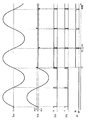
(2.3)動作
次に、電子スイッチ装置1及び電子スイッチシステム10の動作について、図4を参照して説明する。
(2.3) Operation Next, operations of the
図4では、第1電子スイッチ装置1A及び第2電子スイッチ装置1Bの両方のスイッチ部Q1がオフ状態にある状態から、時点t1にて、第2電子スイッチ装置1Bのスイッチ部Q1がオン状態に移行する場合の動作を例示する。図4は、上段から順に、交流電圧「Vac」、スイッチ間電圧「Vsw」、第1電子スイッチ装置1Aの監視信号「S1a」、第2電子スイッチ装置1Bの監視信号「S1b」、第2電子スイッチ装置1Bのスイッチ部Q1の導通/非導通を示している。スイッチ部Q1の導通/非導通を表す「Q1」については、「ON」が導通を表し、「OFF」が非導通を表す。図4の例では、監視信号S1a,S1bの信号レベルは、スイッチ間電圧Vswの絶対値が基準値Vth1以上のときにLレベル(Low level)、スイッチ間電圧Vswの絶対値が基準値Vth1未満のときにHレベル(High level)である。
In FIG. 4, the switch part Q1 of the second
まず、第1電子スイッチ装置1A及び第2電子スイッチ装置1Bの両方のスイッチ部Q1がオフ状態であるときの動作について説明する。
First, an operation when both the switch parts Q1 of the first
この状態では、第1電子スイッチ装置1A及び第2電子スイッチ装置1Bの両方のスイッチ部がオフ状態であるので、スイッチ間電圧Vswは、交流電圧Vacと同電圧となる。図4では、第1電子スイッチ装置1Aにおけるスイッチ部Q1の両端電圧を示しているが、第2電子スイッチ装置1Bにおけるスイッチ部Q1の両端電圧も、第1電子スイッチ装置1Aにおけるスイッチ部Q1の両端電圧と同じである。
In this state, since the switch parts of both the first
この状態においては、2つの電子スイッチ装置1A,1Bのいずれでも、交流電圧Vacの1周期のうちの殆どの期間において、スイッチ間電圧Vswが十分に大きくなる。そのため、2つの電子スイッチ装置1A,1Bのいずれでも、交流電圧Vacの1周期のうちの殆どの期間において、スイッチ間電圧Vswが最低充電電圧以上となり、電源部42に供給電力が供給されて電源部42での制御電源の生成が可能となる。
In this state, in both of the two
次に、第2電子スイッチ装置1Bのスイッチ部Q1がオン状態であるときの動作について説明する。第1電子スイッチ装置1Aのスイッチ部Q1はオフ状態を維持している。
Next, an operation when the switch part Q1 of the second
時点t1にて、第2電子スイッチ装置1Bのスイッチ部Q1がオン状態に移行すると、第2電子スイッチ装置1Bのスイッチ部Q1が導通している間は、スイッチ部Q1の両端間が短絡されるのでスイッチ間電圧Vswが略0〔V〕となる。第2電子スイッチ装置1Bのスイッチ部Q1は、交流電圧Vacのゼロクロス点(0〔V〕)付近、つまり時点t2で非導通となる。その後、スイッチ間電圧Vswの大きさ(絶対値)が基準値Vth1未満である間は、監視信号S1a,S1bはHレベルであるが、スイッチ間電圧Vswの大きさ(絶対値)が基準値Vth1以上になると、監視信号S1a,S1bはLレベルになる。そのため、図4の例では、スイッチ間電圧Vswの大きさ(絶対値)が基準値Vth1に達する時点t3までの期間は監視信号S1a,S1bはHレベルであって、時点t3で監視信号S1a,S1bはLレベルになる。
When the switch part Q1 of the second
監視信号S1bがLレベルになると、第2電子スイッチ装置1Bの制御部5は、スイッチ部Q1を導通させる。そのため、時点t3の直後の時点t4においては、第2電子スイッチ装置1Bのスイッチ部Q1は導通し、スイッチ間電圧Vswが略0〔V〕となる。よって、時点t4にて、監視信号S1a,S1bはHレベルになる。第2電子スイッチ装置1Bのスイッチ部Q1がオン状態である間は、第2電子スイッチ装置1Bは上述の動作を繰り返すことにより、スイッチ間電圧Vswは、時点t2から時点t4までの期間に、間欠的に発生する。
When the monitoring signal S1b becomes L level, the
この状態においては、スイッチ部Q1がオフ状態にある第1電子スイッチ装置1Aでは、交流電圧Vacの1周期のうちの時点t2から時点t4までの期間に、電源部42での制御電源の生成が可能である。また、スイッチ部Q1がオン状態にある第2電子スイッチ装置1Bにおいても、第1電子スイッチ装置1Aと同様に、交流電圧Vacの1周期のうちの時点t2から時点t4までの期間に、電源部42での制御電源の生成が可能である。つまり、電子スイッチ装置1では、上述したようにスイッチ間電圧Vswが最低充電電圧以上であれば、給電回路41から電源部42に供給電力が供給され、電源部42での制御電源の生成が可能である。したがって、スイッチ間電圧Vswが比較的低い場合でも、最低充電電圧以上のスイッチ間電圧Vswが生じてさえいれば、電源部42での制御電源の生成が可能である。
In this state, in the first
一例として、電圧監視部32にてスイッチ間電圧Vswの大きさ(絶対値)と比較される基準値Vth1が、最低充電電圧以上であれば、交流電圧Vacの1周期のうちの時点t2から時点t4までの期間に、電源部42での制御電源の生成が可能となる。つまり、基準値Vth1が最低充電電圧以上であれば、スイッチ部Q1が非導通になった後、スイッチ部Q1が再び導通するまでの間に、スイッチ間電圧Vswは必ず最低充電電圧以上となるので、電源部42での制御電源の生成が可能である。
As an example, if the reference value Vth1 compared with the magnitude (absolute value) of the inter-switch voltage Vsw in the
(3)利点
以上説明したように、第1の態様に係る電子スイッチ装置1は、スイッチ部Q1と、電源部42と、制御部5と、給電回路41と、を備えている。スイッチ部Q1は、交流電源11と負荷12との間に電気的に接続され、交流電源11と負荷12との間の導通/非導通を切り替える。電源部42は、スイッチ部Q1の両端間に電気的に接続され、交流電源11からの供給電力により制御電源を生成する。制御部5は、電源部42から上記制御電源の供給を受けて動作し、スイッチ部Q1を制御する。給電回路41は、スイッチ部Q1の両端間に電気的に接続され、スイッチ部Q1と電源部42との間における上記供給電力の単一の経路となる。給電回路41は、スイッチ部Q1の両端間の電圧の大きさが所定値以上になれば電源部42に上記供給電力を供給するように構成されている。
(3) Advantages As described above, the
この構成によれば、交流電源11からの供給電力により制御電源を生成する電源部42には、給電回路41からなる単一の経路を通して、供給電力が供給される。すなわち、交流電源11から電源部42への供給電力の経路は、スイッチ部Q1と電源部42との間に一つだけ存在するのであって、給電回路41以外には、電源部42への供給電力の経路は存在しない。しかも、給電回路41は、スイッチ部Q1の両端間の電圧の大きさが所定値(最低充電電圧)以上になれば電源部42に上記供給電力を供給する。よって、給電回路41は、電源部42への供給電力の経路を切り替えることなく、スイッチ部Q1がオン状態及びオフ状態のいずれにあっても、電源部42には、常に同一の経路にて、供給電力が供給される。結果的に、電子スイッチ装置1では、負荷12の通電時に制御電源を確保するためにカレントトランスが必要でなく、小型化が可能である。さらに、電子スイッチ装置1では、電源部42への供給電力の経路を切り替えるための構成、及び電源部42への供給電力の経路を切り替えるための複雑な制御も不要であるから、より小型化が可能である。
According to this configuration, the supply power is supplied to the
また、第2の態様に係る電子スイッチ装置1では、第1の態様において、電源部42はコンデンサC1を有することが好ましい。この場合、給電回路41は、スイッチ部Q1の両端間におけるコンデンサC1の充電経路40に設けられ、スイッチ部Q1の両端間の電圧の大きさが所定値以上のときにオンする電圧駆動型の能動素子Q10を有することが好ましい。この構成によれば、上述した比較例のように、給電回路41にバイポーラトランジスタを適用した構成に比べて、スイッチ間電圧Vswがより低い電圧でも、コンデンサC1を充電して制御電源を確保することが可能である。ただし、この構成は電子スイッチ装置1に必須の構成ではなく、例えば、能動素子Q10は電圧駆動型の素子でなくてもよい。
Moreover, in the
また、第3の態様に係る電子スイッチ装置1では、第2の態様において、能動素子Q10は電界効果トランジスタ(FET)であることが好ましい。この構成によれば、特殊な部品を用いることなく、給電回路41を実現することが可能である。ただし、この構成は電子スイッチ装置1に必須の構成ではなく、能動素子Q10は例えばIGBT(Insulated Gate Bipolar Transistor)などであってもよい。
In the
また、第4の態様に係る電子スイッチ装置1では、第1〜3のいずれかの態様において、給電回路41は、交流電源11から電源部42に規定値以上の電流が流れると、電源部42への供給電力の供給を停止させる電流制限部43を有することが好ましい。この構成によれば、給電回路41に流れる電流が制限されることにより、給電回路41の構成部品に掛かるストレスを低減でき、給電回路41に要求される電流容量を小さくできる。さらに、電流制限部43によれば、例えば交流電源11の投入時などに給電回路41に流れる突入電流を抑制することにより、負荷12が誤動作(例えばフラッシュ現象の発生など)することも抑制可能である。ただし、この構成は電子スイッチ装置1に必須の構成ではなく、例えば、能動素子Q10に電流容量の大きな素子を適用したり、コンデンサC1に静電容量の小さな素子を適用したりすることで、電流制限部43は省略されていてもよい。
Further, in the
また、第5の態様に係る電子スイッチ装置1は、第1〜4のいずれかの態様において、センサ部31を更に備え、制御部5は、センサ部31の出力に基づいてスイッチ部Q1を制御するように構成されていることが好ましい。この構成によれば、電源部42で生成される制御電源にてセンサ部31を駆動でき、センサ部31の出力によってスイッチ部Q1を自動的に制御することが可能である。ただし、この構成は電子スイッチ装置1に必須の構成ではなく、センサ部31は適宜省略される。
Moreover, the
また、電子スイッチシステム10は、第1〜5のいずれかの態様に係る電子スイッチ装置1を複数備え、複数の電子スイッチ装置1が備える複数のスイッチ部Q1は、交流電源11と負荷12との間に電気的に並列に接続される。
The
言い換えれば、電子スイッチシステム10は、複数の電子スイッチ装置1を備え、これら複数の電子スイッチ装置1の各々は、スイッチ部Q1と、電源部42と、制御部5と、給電回路41と、を備えている。スイッチ部Q1は、交流電源11と負荷12との間に電気的に接続され、交流電源11と負荷12との間の導通/非導通を切り替える。電源部42は、スイッチ部Q1の両端間に電気的に接続され、交流電源11からの供給電力により制御電源を生成する。制御部5は、電源部42から上記制御電源の供給を受けて動作し、スイッチ部Q1を制御する。給電回路41は、スイッチ部Q1の両端間に電気的に接続され、スイッチ部Q1と電源部42との間における上記供給電力の単一の経路となる。給電回路41は、スイッチ部Q1の両端間の電圧の大きさが所定値以上になれば電源部42に上記供給電力を供給するように構成されている。複数の電子スイッチ装置1がそれぞれ備える複数のスイッチ部Q1は、交流電源11と負荷12との間に電気的に並列に接続される。
In other words, the
この構成によれば、複数の電子スイッチ装置1の各々において、給電回路41は、電源部42への供給電力の経路を切り替えることなく、スイッチ部Q1がオン状態及びオフ状態のいずれにあっても、電源部42には、常に同一の経路にて、供給電力が供給される。結果的に、各電子スイッチ装置1では、負荷12の通電時に制御電源を確保するためにカレントトランスが必要でなく、小型化が可能である。さらに、各電子スイッチ装置1では、電源部42への供給電力の経路を切り替えるための構成、及び電源部42への供給電力の経路を切り替えるための複雑な制御も不要であるから、より小型化が可能である。とくに、三路スイッチからなる電子スイッチ装置1を2つ組み合わせた電子スイッチシステム10では、スイッチ部Q1がオフ状態の電子スイッチ装置1Aと、スイッチ部Q1がオン状態の電子スイッチ装置1Bとのいずれでも、制御電源を確保可能である。
According to this configuration, in each of the plurality of
(4)変形例
実施形態1に係る電子スイッチ装置1は、本発明の一例に過ぎず、本発明は、実施形態1に限定されることはなく、実施形態1以外であっても、本発明に係る技術的思想を逸脱しない範囲であれば、設計等に応じて種々の変更が可能である。以下に、実施形態1の変形例を列挙する。
(4) Modification The
負荷12は照明装置に限らず、例えば、換気扇及び防犯機器等の電気機器であってもよい。また、負荷12は、1台の電気機器に限らず、電気的に直列又は並列に接続された複数台の電気機器であってもよい。
The
また、スイッチ部Q1は双方向サイリスタに限らず、その他の半導体スイッチであってもよい。スイッチ部Q1は、例えば、第1の接続端子101と第3の接続端子103との間に電気的に直列に接続された、2つのMOSFETであってもよい。2つのMOSFETは、ソース端子同士が互いに接続される、つまり、いわゆる逆直列に接続されることにより、双方向の電流の通過/遮断を切り替える。さらにまた、スイッチ部Q1は、例えば、GaN(窒化ガリウム)などのワイドバンドギャップの半導体材料を用いたダブルゲート(デュアルゲート)構造の半導体素子であってもよい。
The switch unit Q1 is not limited to a bidirectional thyristor, and may be another semiconductor switch. The switch part Q1 may be two MOSFETs electrically connected in series between the
また、スイッチ部Q1を駆動するための駆動回路が、制御部5とは別に設けられていてもよい。この場合、制御電源は、駆動回路の動作にも使用される。
Further, a drive circuit for driving the switch unit Q1 may be provided separately from the
また、センサ部31は、人が存在するか否かを検知する人感センサに限らず、例えば、明るさセンサであってもよい。又は、センサ部31は、人感センサと明るさセンサとの両方を有していてもよい。さらに、電子スイッチ装置1は、センサ部31の検知結果に基づいてスイッチ部Q1が制御される構成に限らず、例えば、遠隔操作機能、タイマ機能、又は調光機能付きの電子スイッチ装置であってもよい。例えば遠隔操作機能付きの電子スイッチ装置1であれば、制御部5は、リモートコントローラからのワイヤレス信号に基づいて、スイッチ部Q1を制御する。さらにまた、電子スイッチ装置1は、例えば、押ボタンスイッチ又はタッチスイッチ等の操作部に対する人の操作に基づいて、スイッチ部Q1が制御される構成であってもよい。
The
また、電圧監視部32は、全波整流後のスイッチ間電圧Vswではなく、全波整流前のスイッチ間電圧Vswの大きさを監視する構成であってもよい。この場合、電圧監視部32は、整流器2の交流入力端子間に電気的に接続される。さらに、電圧監視部32は、交流電圧Vacのゼロクロス点を検出するためのゼロクロス検出部と兼用されていてもよい。ゼロクロス検出部は、スイッチ間電圧Vswが、0〔V〕付近に設定された基準値(絶対値)未満から基準値以上に移行したことをもって、ゼロクロス点を検出する。
Further, the
また、電圧監視部32は、電子スイッチ装置1に必須の構成ではなく、省略されていてもよい。この場合、制御部5は、例えば、コンデンサC1の両端電圧の検出結果に基づいて、スイッチ部Q1を制御してもよい。具体的には、制御部5は、コンデンサC1の両端電圧が所定の閾値に達した際に、スイッチ部Q1を導通させる。ここでいう閾値は、少なくとも次に能動素子Q10がオンする時点までの制御部5等の動作を確保できる程度に、コンデンサC1が充電されたときのコンデンサC1の両端電圧である。
Further, the
また、給電回路41及び電源部42の具体回路は、図3に示す回路に限らず、適宜変更が可能である。例えば、給電回路41は、ツェナダイオードZD1及び能動素子Q10に加え、オペアンプを有する定電圧回路であってもよいし、能動素子Q10が省略されていてもよい。電流制限部43のスイッチ素子Q11は、バイポーラトランジスタに限らず、例えばエンハンスメント形のnチャネルMOSFETなどであってもよい。電源部42については、例えば、コンデンサC1はレギュレータ44の出力に接続されていてもよいし、コンデンサC1とは別のコンデンサがレギュレータ44の出力に接続されていてもよい。さらに、電源部42におけるレギュレータ44は電子スイッチ装置1に必須の構成ではなく、レギュレータ44は省略されてもよい。
The specific circuits of the
また、実施形態1にて、スイッチ間電圧及び基準値等の2値間の比較において、「以上」としているところは、2値が等しい場合、及び2値の一方が他方を超えている場合との両方を含む。ただし、これに限らず、ここでいう「以上」は、2値の一方が他方を超えている場合のみを含む「より大きい」と同義であってもよい。つまり、2値が等しい場合を含むか否かは、基準値等の設定次第で任意に変更できるので、「以上」か「より大きい」かに技術上の差異はない。同様に、「未満」においても「以下」と同義であってもよい。 In the first embodiment, in the comparison between the two values such as the voltage between the switches and the reference value, “more than” is the case where the two values are equal and the case where one of the two values exceeds the other. Including both. However, the present invention is not limited to this, and “more than” here may be synonymous with “greater than” including only when one of the binary values exceeds the other. That is, whether or not the case where the two values are equal can be arbitrarily changed depending on the setting of the reference value or the like, so there is no technical difference between “greater than” or “greater than”. Similarly, “less than” may be synonymous with “below”.
(実施形態2)
実施形態2に係る電子スイッチシステム10Aは、図5に示すように、3つの電子スイッチ装置1A,1B,1Cの組み合わせからなる。以下、実施形態1と同様の構成については、共通の符号を付して適宜説明を省略する。
(Embodiment 2)
As shown in FIG. 5, the
電子スイッチ装置1A,1Bは、実施形態1と同様、いわゆる三路スイッチである。一方、電子スイッチ装置1Cは、4本の配線を接続可能な、いわゆる四路スイッチである。電子スイッチ装置1Cは、電子スイッチ装置1A,1Bと同様の3つの接続端子101,102,103に加えて、第4の接続端子104を備えている。
The
電子スイッチ装置1Cにおいて、接続端子103と接続端子104とは電子スイッチ装置1Cの内部で接続されている。電子スイッチ装置1Aの接続端子102は、電子スイッチ装置1Cの接続端子101に接続されている。電子スイッチ装置1Aの接続端子103は、電子スイッチ装置1Cの接続端子104に接続されている。電子スイッチ装置1Bの接続端子102は、電子スイッチ装置1Cの接続端子103に接続されている。電子スイッチ装置1Bの接続端子103は、電子スイッチ装置1Cの接続端子102に接続されている。
In the electronic switch device 1C, the
上述の接続関係によれば、複数(ここでは3つ)の電子スイッチ装置1A,1B,1Cがそれぞれ備える複数のスイッチ部Q1は、交流電源11と負荷12との間に電気的に並列に接続される。そのため、3つの電子スイッチ装置1A,1B,1Cのいずれかのスイッチ部Q1が導通していれば、交流電源11と負荷12との間が導通し、3つの電子スイッチ装置1A,1B,1Cを介して、交流電源11から負荷12に電力供給される。したがって、電子スイッチシステム10Aでは、電子スイッチ装置1Aのスイッチ部Q1、電子スイッチ装置1Bのスイッチ部Q1、及び電子スイッチ装置1Cのスイッチ部Q1の全てにおいて、負荷12への通電状態を切り替えることが可能である。よって、3つの電子スイッチ装置1A,1B,1Cを組み合わせた電子スイッチシステム10Aでは、負荷12への通電状態を、3箇所で切り替えることが可能である。
According to the connection relation described above, the plurality of switch units Q1 included in each of the plurality (here, three) of
以上説明した本実施形態の電子スイッチシステム10Aにおいても、実施形態1と同様に、負荷12の通電時に制御電源を確保するためにカレントトランスが必要でなく、電子スイッチ装置1の小型化が可能である、という利点がある。
Also in the
また、実施形態2の変形例として、電子スイッチシステム10Aは、電子スイッチ装置1C(いわゆる四路スイッチ)を2つ以上備え、計4つ以上の電子スイッチ装置1A,1B,1Cを備えていてもよい。この場合、複数の電子スイッチ装置1A,1B,1Cがそれぞれ備える複数のスイッチ部Q1が、交流電源11と負荷12との間に電気的に並列に接続されることで、負荷12への通電状態を、4箇所以上で切り替えることが可能である。
As a modification of the second embodiment, the
実施形態2の構成(変形例を含む)は、実施形態1の構成(変形例を含む)と適宜組み合わせて適用可能である。 The configuration of the second embodiment (including modifications) can be applied in appropriate combination with the configuration of the first embodiment (including modifications).
(実施形態3)
実施形態3に係る電子スイッチ装置1Dは、図6に示すように、2本の配線を接続可能な、いわゆる片切スイッチである。以下、実施形態1と同様の構成については、共通の符号を付して適宜説明を省略する。
(Embodiment 3)
The
電子スイッチ装置1Dは、2つの接続端子101,103を備えている。言い換えれば、電子スイッチ装置1Dは、実施形態1の電子スイッチ装置1A(図2参照)から、3つの接続端子101,102,103のうちの接続端子102が省略された構成である。
The
図6の例では、電子スイッチ装置1Dの接続端子101は負荷12に接続され、電子スイッチ装置1Dの接続端子103は交流電源11に接続されている。この接続関係によれば、電子スイッチ装置1Dのスイッチ部Q1は、交流電源11と負荷12との間に電気的に接続される。そのため、電子スイッチ装置1Dのスイッチ部Q1が導通していれば、交流電源11と負荷12との間が導通し、電子スイッチ装置1Dを介して、交流電源11から負荷12に電力供給される。
In the example of FIG. 6, the
以上説明した本実施形態の電子スイッチ装置1Dにおいても、実施形態1と同様に、負荷12の通電時に制御電源を確保するためにカレントトランスが必要でなく、小型化が可能である、という利点がある。
Also in the
実施形態3の構成は、実施形態1の構成(変形例を含む)と適宜組み合わせて適用可能である。 The configuration of the third embodiment can be applied in combination with the configuration of the first embodiment (including modifications) as appropriate.
1,1A,1B,1C,1D 電子スイッチ装置
5 制御部
10,10A 電子スイッチシステム
11 交流電源
12 負荷
31 センサ部
40 充電経路
41 給電回路
42 電源部
43 電流制限部
C1 コンデンサ
Q1 スイッチ部
Q10 能動素子
1, 1A, 1B, 1C, 1D
Claims (6)
前記スイッチ部の両端間に電気的に接続され、前記交流電源からの供給電力により制御電源を生成する電源部と、
前記電源部から前記制御電源の供給を受けて動作し、前記スイッチ部を制御する制御部と、
前記スイッチ部の両端間に電気的に接続され、前記スイッチ部と前記電源部との間における前記供給電力の単一の経路となる給電回路と、を備え、
前記給電回路は、前記スイッチ部の前記両端間の電圧の大きさが所定値以上になれば前記電源部に前記供給電力を供給するように構成されている
電子スイッチ装置。 A switch unit that is electrically connected between an AC power source and a load, and switches between conduction and non-conduction between the AC power source and the load;
A power supply unit that is electrically connected between both ends of the switch unit and generates a control power supply by power supplied from the AC power supply;
A control unit that operates by receiving the control power supply from the power supply unit, and controls the switch unit;
A power supply circuit that is electrically connected between both ends of the switch unit and serves as a single path of the supplied power between the switch unit and the power supply unit,
The power supply circuit is configured to supply the supply power to the power supply unit when the voltage across the switch unit reaches a predetermined value or more.
前記給電回路は、前記スイッチ部の前記両端間における前記コンデンサの充電経路に設けられ、前記スイッチ部の前記両端間の電圧の大きさが前記所定値以上のときにオンする電圧駆動型の能動素子を有する
請求項1に記載の電子スイッチ装置。 The power supply unit has a capacitor,
The power supply circuit is provided in a charging path of the capacitor between the both ends of the switch unit, and is turned on when a voltage magnitude between the both ends of the switch unit is equal to or greater than the predetermined value. The electronic switch device according to claim 1.
請求項2に記載の電子スイッチ装置。 The electronic switch device according to claim 2, wherein the active element is a field effect transistor.
請求項1〜3のいずれか1項に記載の電子スイッチ装置。 The power supply circuit includes a current limiting unit that stops supply of the supplied power to the power supply unit when a current of a specified value or more flows from the AC power supply to the power supply unit. The electronic switch device described in 1.
前記制御部は、前記センサ部の出力に基づいて前記スイッチ部を制御するように構成されている
請求項1〜4のいずれか1項に記載の電子スイッチ装置。 A sensor unit;
The electronic switch device according to claim 1, wherein the control unit is configured to control the switch unit based on an output of the sensor unit.
前記複数の電子スイッチ装置が備える複数のスイッチ部は、交流電源と負荷との間に電気的に並列に接続される
電子スイッチシステム。 A plurality of electronic switch devices according to any one of claims 1 to 5,
The plurality of switch units included in the plurality of electronic switch devices are electrically connected in parallel between an AC power source and a load.
Priority Applications (3)
| Application Number | Priority Date | Filing Date | Title |
|---|---|---|---|
| JP2016062510A JP6635301B2 (en) | 2016-03-25 | 2016-03-25 | Electronic switch device and electronic switch system |
| PCT/JP2017/010338 WO2017164029A1 (en) | 2016-03-25 | 2017-03-15 | Electronic switch device and electronic switch system |
| TW106109063A TWI627831B (en) | 2016-03-25 | 2017-03-20 | Electronic switch device and electronic switch system |
Applications Claiming Priority (1)
| Application Number | Priority Date | Filing Date | Title |
|---|---|---|---|
| JP2016062510A JP6635301B2 (en) | 2016-03-25 | 2016-03-25 | Electronic switch device and electronic switch system |
Publications (2)
| Publication Number | Publication Date |
|---|---|
| JP2017174765A true JP2017174765A (en) | 2017-09-28 |
| JP6635301B2 JP6635301B2 (en) | 2020-01-22 |
Family
ID=59900446
Family Applications (1)
| Application Number | Title | Priority Date | Filing Date |
|---|---|---|---|
| JP2016062510A Active JP6635301B2 (en) | 2016-03-25 | 2016-03-25 | Electronic switch device and electronic switch system |
Country Status (3)
| Country | Link |
|---|---|
| JP (1) | JP6635301B2 (en) |
| TW (1) | TWI627831B (en) |
| WO (1) | WO2017164029A1 (en) |
Cited By (2)
| Publication number | Priority date | Publication date | Assignee | Title |
|---|---|---|---|---|
| KR101885308B1 (en) * | 2018-03-20 | 2018-08-03 | 손성민 | DC Adapter for Magnetic Contactor Drive |
| JP2021153302A (en) * | 2017-10-10 | 2021-09-30 | イクシス・リミテッド・ライアビリティ・カンパニーIxys, Llc | Self-powered electronic fuse |
Families Citing this family (1)
| Publication number | Priority date | Publication date | Assignee | Title |
|---|---|---|---|---|
| US10177645B2 (en) * | 2017-06-12 | 2019-01-08 | Semiconductor Components Industries, Llc | Synchronous rectifier turn-on enable |
Family Cites Families (5)
| Publication number | Priority date | Publication date | Assignee | Title |
|---|---|---|---|---|
| JPS6269761A (en) * | 1985-09-21 | 1987-03-31 | Nec Corp | Automatic re-build-up device for electronic switching system |
| KR101760276B1 (en) * | 2010-11-16 | 2017-07-21 | 삼성전자주식회사 | Apparaus and Method for Switch Mode Power Supply |
| CN202004651U (en) * | 2011-02-17 | 2011-10-05 | 昂宝电子(上海)有限公司 | Switching power supply circuit for flyback structure |
| CN102195492B (en) * | 2011-05-24 | 2014-04-16 | 成都芯源系统有限公司 | Synchronous rectification switching power supply and control circuit and control method thereof |
| CN105247772B (en) * | 2013-05-20 | 2018-07-24 | 松下知识产权经营株式会社 | DC power supply circuit |
-
2016
- 2016-03-25 JP JP2016062510A patent/JP6635301B2/en active Active
-
2017
- 2017-03-15 WO PCT/JP2017/010338 patent/WO2017164029A1/en active Application Filing
- 2017-03-20 TW TW106109063A patent/TWI627831B/en active
Cited By (4)
| Publication number | Priority date | Publication date | Assignee | Title |
|---|---|---|---|---|
| JP2021153302A (en) * | 2017-10-10 | 2021-09-30 | イクシス・リミテッド・ライアビリティ・カンパニーIxys, Llc | Self-powered electronic fuse |
| JP7288003B2 (en) | 2017-10-10 | 2023-06-06 | イクシス・リミテッド・ライアビリティ・カンパニー | self-powered electronic fuse |
| KR101885308B1 (en) * | 2018-03-20 | 2018-08-03 | 손성민 | DC Adapter for Magnetic Contactor Drive |
| US10504674B2 (en) | 2018-03-20 | 2019-12-10 | Yeon Hee Seo | DC adaptor for driving magnetic contactor |
Also Published As
| Publication number | Publication date |
|---|---|
| TW201735538A (en) | 2017-10-01 |
| TWI627831B (en) | 2018-06-21 |
| JP6635301B2 (en) | 2020-01-22 |
| WO2017164029A1 (en) | 2017-09-28 |
Similar Documents
| Publication | Publication Date | Title |
|---|---|---|
| TWI584693B (en) | Dimming device | |
| TWI580183B (en) | Switch device and load control system ???including the same | |
| JP6751908B2 (en) | Electronic switch device and electronic switch system | |
| TWI657718B (en) | Dimming device | |
| WO2017164029A1 (en) | Electronic switch device and electronic switch system | |
| TWI618451B (en) | Protection circuit and wiring device | |
| JP6563648B2 (en) | Insulated DC / DC converter, primary side controller, synchronous rectification controller, power supply device using the same, power supply adapter, and electronic device | |
| TWI565363B (en) | Switch device | |
| JP7026320B2 (en) | Electronic switch device | |
| JP7390589B2 (en) | Switching control device and switching control system | |
| JP6830224B2 (en) | Electronic switch device and electronic switch system | |
| WO2017164028A1 (en) | Electronic switch device and electronic switch system | |
| JP7555048B2 (en) | Load Control Device | |
| JP6796805B2 (en) | Electronic switch device and electronic switch system | |
| CN111384937B (en) | Load control circuit, load control method, and storage medium | |
| TW202114470A (en) | Load control device | |
| JP5773180B2 (en) | Load control device | |
| TWM582262U (en) | Sensing type power supply control device |
Legal Events
| Date | Code | Title | Description |
|---|---|---|---|
| RD02 | Notification of acceptance of power of attorney |
Free format text: JAPANESE INTERMEDIATE CODE: A7422 Effective date: 20170124 |
|
| A621 | Written request for application examination |
Free format text: JAPANESE INTERMEDIATE CODE: A621 Effective date: 20190123 |
|
| TRDD | Decision of grant or rejection written | ||
| A01 | Written decision to grant a patent or to grant a registration (utility model) |
Free format text: JAPANESE INTERMEDIATE CODE: A01 Effective date: 20191105 |
|
| A61 | First payment of annual fees (during grant procedure) |
Free format text: JAPANESE INTERMEDIATE CODE: A61 Effective date: 20191204 |
|
| R151 | Written notification of patent or utility model registration |
Ref document number: 6635301 Country of ref document: JP Free format text: JAPANESE INTERMEDIATE CODE: R151 |