JP2017168530A - Compound semiconductor device and manufacturing method thereof - Google Patents
Compound semiconductor device and manufacturing method thereof Download PDFInfo
- Publication number
- JP2017168530A JP2017168530A JP2016050147A JP2016050147A JP2017168530A JP 2017168530 A JP2017168530 A JP 2017168530A JP 2016050147 A JP2016050147 A JP 2016050147A JP 2016050147 A JP2016050147 A JP 2016050147A JP 2017168530 A JP2017168530 A JP 2017168530A
- Authority
- JP
- Japan
- Prior art keywords
- layer
- compound semiconductor
- source electrode
- electrode
- groove
- Prior art date
- Legal status (The legal status is an assumption and is not a legal conclusion. Google has not performed a legal analysis and makes no representation as to the accuracy of the status listed.)
- Pending
Links
- 239000004065 semiconductor Substances 0.000 title claims abstract description 100
- 150000001875 compounds Chemical class 0.000 title claims abstract description 97
- 238000004519 manufacturing process Methods 0.000 title claims description 34
- 238000000034 method Methods 0.000 claims description 44
- 238000013459 approach Methods 0.000 claims description 10
- 230000004888 barrier function Effects 0.000 description 81
- 229910000530 Gallium indium arsenide Inorganic materials 0.000 description 63
- 238000012986 modification Methods 0.000 description 62
- 230000004048 modification Effects 0.000 description 48
- 229910004298 SiO 2 Inorganic materials 0.000 description 42
- 125000006850 spacer group Chemical group 0.000 description 31
- 229910000980 Aluminium gallium arsenide Inorganic materials 0.000 description 20
- 229910017115 AlSb Inorganic materials 0.000 description 16
- 229910001218 Gallium arsenide Inorganic materials 0.000 description 16
- 229910000577 Silicon-germanium Inorganic materials 0.000 description 16
- 239000000758 substrate Substances 0.000 description 16
- 229910000673 Indium arsenide Inorganic materials 0.000 description 15
- KRKNYBCHXYNGOX-UHFFFAOYSA-N citric acid Chemical compound OC(=O)CC(O)(C(O)=O)CC(O)=O KRKNYBCHXYNGOX-UHFFFAOYSA-N 0.000 description 15
- 230000000052 comparative effect Effects 0.000 description 14
- 230000008569 process Effects 0.000 description 13
- 238000010586 diagram Methods 0.000 description 12
- 238000005530 etching Methods 0.000 description 12
- 230000005684 electric field Effects 0.000 description 11
- WPYVAWXEWQSOGY-UHFFFAOYSA-N indium antimonide Chemical compound [Sb]#[In] WPYVAWXEWQSOGY-UHFFFAOYSA-N 0.000 description 11
- RPQDHPTXJYYUPQ-UHFFFAOYSA-N indium arsenide Chemical compound [In]#[As] RPQDHPTXJYYUPQ-UHFFFAOYSA-N 0.000 description 11
- 229910002704 AlGaN Inorganic materials 0.000 description 10
- 238000010894 electron beam technology Methods 0.000 description 9
- 230000003071 parasitic effect Effects 0.000 description 9
- 239000007789 gas Substances 0.000 description 7
- 238000001020 plasma etching Methods 0.000 description 7
- 238000004904 shortening Methods 0.000 description 7
- 239000012212 insulator Substances 0.000 description 6
- 238000005268 plasma chemical vapour deposition Methods 0.000 description 6
- 238000004088 simulation Methods 0.000 description 6
- MHAJPDPJQMAIIY-UHFFFAOYSA-N Hydrogen peroxide Chemical compound OO MHAJPDPJQMAIIY-UHFFFAOYSA-N 0.000 description 5
- 238000004380 ashing Methods 0.000 description 5
- 230000015572 biosynthetic process Effects 0.000 description 5
- 239000011259 mixed solution Substances 0.000 description 5
- 239000000243 solution Substances 0.000 description 5
- 239000000126 substance Substances 0.000 description 5
- 230000007423 decrease Effects 0.000 description 4
- 230000000694 effects Effects 0.000 description 3
- 239000007772 electrode material Substances 0.000 description 3
- 238000007740 vapor deposition Methods 0.000 description 3
- 230000008859 change Effects 0.000 description 2
- 238000005229 chemical vapour deposition Methods 0.000 description 1
- 238000004891 communication Methods 0.000 description 1
- 239000013078 crystal Substances 0.000 description 1
- 238000010438 heat treatment Methods 0.000 description 1
- 239000012535 impurity Substances 0.000 description 1
- 238000011835 investigation Methods 0.000 description 1
- 238000002955 isolation Methods 0.000 description 1
- 239000002184 metal Substances 0.000 description 1
- 238000002488 metal-organic chemical vapour deposition Methods 0.000 description 1
- 238000001451 molecular beam epitaxy Methods 0.000 description 1
- 238000000206 photolithography Methods 0.000 description 1
- 230000009467 reduction Effects 0.000 description 1
- 230000003068 static effect Effects 0.000 description 1
- 238000001039 wet etching Methods 0.000 description 1
Images


Classifications
-
- H—ELECTRICITY
- H01—ELECTRIC ELEMENTS
- H01L—SEMICONDUCTOR DEVICES NOT COVERED BY CLASS H10
- H01L29/00—Semiconductor devices specially adapted for rectifying, amplifying, oscillating or switching and having potential barriers; Capacitors or resistors having potential barriers, e.g. a PN-junction depletion layer or carrier concentration layer; Details of semiconductor bodies or of electrodes thereof ; Multistep manufacturing processes therefor
- H01L29/66—Types of semiconductor device ; Multistep manufacturing processes therefor
- H01L29/68—Types of semiconductor device ; Multistep manufacturing processes therefor controllable by only the electric current supplied, or only the electric potential applied, to an electrode which does not carry the current to be rectified, amplified or switched
- H01L29/76—Unipolar devices, e.g. field effect transistors
- H01L29/772—Field effect transistors
- H01L29/778—Field effect transistors with two-dimensional charge carrier gas channel, e.g. HEMT ; with two-dimensional charge-carrier layer formed at a heterojunction interface
- H01L29/7786—Field effect transistors with two-dimensional charge carrier gas channel, e.g. HEMT ; with two-dimensional charge-carrier layer formed at a heterojunction interface with direct single heterostructure, i.e. with wide bandgap layer formed on top of active layer, e.g. direct single heterostructure MIS-like HEMT
-
- H—ELECTRICITY
- H01—ELECTRIC ELEMENTS
- H01L—SEMICONDUCTOR DEVICES NOT COVERED BY CLASS H10
- H01L29/00—Semiconductor devices specially adapted for rectifying, amplifying, oscillating or switching and having potential barriers; Capacitors or resistors having potential barriers, e.g. a PN-junction depletion layer or carrier concentration layer; Details of semiconductor bodies or of electrodes thereof ; Multistep manufacturing processes therefor
- H01L29/02—Semiconductor bodies ; Multistep manufacturing processes therefor
- H01L29/06—Semiconductor bodies ; Multistep manufacturing processes therefor characterised by their shape; characterised by the shapes, relative sizes, or dispositions of the semiconductor regions ; characterised by the concentration or distribution of impurities within semiconductor regions
- H01L29/0657—Semiconductor bodies ; Multistep manufacturing processes therefor characterised by their shape; characterised by the shapes, relative sizes, or dispositions of the semiconductor regions ; characterised by the concentration or distribution of impurities within semiconductor regions characterised by the shape of the body
-
- H—ELECTRICITY
- H01—ELECTRIC ELEMENTS
- H01L—SEMICONDUCTOR DEVICES NOT COVERED BY CLASS H10
- H01L29/00—Semiconductor devices specially adapted for rectifying, amplifying, oscillating or switching and having potential barriers; Capacitors or resistors having potential barriers, e.g. a PN-junction depletion layer or carrier concentration layer; Details of semiconductor bodies or of electrodes thereof ; Multistep manufacturing processes therefor
- H01L29/02—Semiconductor bodies ; Multistep manufacturing processes therefor
- H01L29/06—Semiconductor bodies ; Multistep manufacturing processes therefor characterised by their shape; characterised by the shapes, relative sizes, or dispositions of the semiconductor regions ; characterised by the concentration or distribution of impurities within semiconductor regions
- H01L29/0684—Semiconductor bodies ; Multistep manufacturing processes therefor characterised by their shape; characterised by the shapes, relative sizes, or dispositions of the semiconductor regions ; characterised by the concentration or distribution of impurities within semiconductor regions characterised by the shape, relative sizes or dispositions of the semiconductor regions or junctions between the regions
- H01L29/0688—Semiconductor bodies ; Multistep manufacturing processes therefor characterised by their shape; characterised by the shapes, relative sizes, or dispositions of the semiconductor regions ; characterised by the concentration or distribution of impurities within semiconductor regions characterised by the shape, relative sizes or dispositions of the semiconductor regions or junctions between the regions characterised by the particular shape of a junction between semiconductor regions
-
- H—ELECTRICITY
- H01—ELECTRIC ELEMENTS
- H01L—SEMICONDUCTOR DEVICES NOT COVERED BY CLASS H10
- H01L29/00—Semiconductor devices specially adapted for rectifying, amplifying, oscillating or switching and having potential barriers; Capacitors or resistors having potential barriers, e.g. a PN-junction depletion layer or carrier concentration layer; Details of semiconductor bodies or of electrodes thereof ; Multistep manufacturing processes therefor
- H01L29/02—Semiconductor bodies ; Multistep manufacturing processes therefor
- H01L29/12—Semiconductor bodies ; Multistep manufacturing processes therefor characterised by the materials of which they are formed
- H01L29/16—Semiconductor bodies ; Multistep manufacturing processes therefor characterised by the materials of which they are formed including, apart from doping materials or other impurities, only elements of Group IV of the Periodic Table
- H01L29/161—Semiconductor bodies ; Multistep manufacturing processes therefor characterised by the materials of which they are formed including, apart from doping materials or other impurities, only elements of Group IV of the Periodic Table including two or more of the elements provided for in group H01L29/16, e.g. alloys
- H01L29/165—Semiconductor bodies ; Multistep manufacturing processes therefor characterised by the materials of which they are formed including, apart from doping materials or other impurities, only elements of Group IV of the Periodic Table including two or more of the elements provided for in group H01L29/16, e.g. alloys in different semiconductor regions, e.g. heterojunctions
-
- H—ELECTRICITY
- H01—ELECTRIC ELEMENTS
- H01L—SEMICONDUCTOR DEVICES NOT COVERED BY CLASS H10
- H01L29/00—Semiconductor devices specially adapted for rectifying, amplifying, oscillating or switching and having potential barriers; Capacitors or resistors having potential barriers, e.g. a PN-junction depletion layer or carrier concentration layer; Details of semiconductor bodies or of electrodes thereof ; Multistep manufacturing processes therefor
- H01L29/02—Semiconductor bodies ; Multistep manufacturing processes therefor
- H01L29/12—Semiconductor bodies ; Multistep manufacturing processes therefor characterised by the materials of which they are formed
- H01L29/20—Semiconductor bodies ; Multistep manufacturing processes therefor characterised by the materials of which they are formed including, apart from doping materials or other impurities, only AIIIBV compounds
- H01L29/201—Semiconductor bodies ; Multistep manufacturing processes therefor characterised by the materials of which they are formed including, apart from doping materials or other impurities, only AIIIBV compounds including two or more compounds, e.g. alloys
- H01L29/205—Semiconductor bodies ; Multistep manufacturing processes therefor characterised by the materials of which they are formed including, apart from doping materials or other impurities, only AIIIBV compounds including two or more compounds, e.g. alloys in different semiconductor regions, e.g. heterojunctions
-
- H—ELECTRICITY
- H01—ELECTRIC ELEMENTS
- H01L—SEMICONDUCTOR DEVICES NOT COVERED BY CLASS H10
- H01L29/00—Semiconductor devices specially adapted for rectifying, amplifying, oscillating or switching and having potential barriers; Capacitors or resistors having potential barriers, e.g. a PN-junction depletion layer or carrier concentration layer; Details of semiconductor bodies or of electrodes thereof ; Multistep manufacturing processes therefor
- H01L29/40—Electrodes ; Multistep manufacturing processes therefor
- H01L29/41—Electrodes ; Multistep manufacturing processes therefor characterised by their shape, relative sizes or dispositions
- H01L29/423—Electrodes ; Multistep manufacturing processes therefor characterised by their shape, relative sizes or dispositions not carrying the current to be rectified, amplified or switched
- H01L29/42312—Gate electrodes for field effect devices
- H01L29/42316—Gate electrodes for field effect devices for field-effect transistors
- H01L29/4232—Gate electrodes for field effect devices for field-effect transistors with insulated gate
- H01L29/42356—Disposition, e.g. buried gate electrode
-
- H—ELECTRICITY
- H01—ELECTRIC ELEMENTS
- H01L—SEMICONDUCTOR DEVICES NOT COVERED BY CLASS H10
- H01L29/00—Semiconductor devices specially adapted for rectifying, amplifying, oscillating or switching and having potential barriers; Capacitors or resistors having potential barriers, e.g. a PN-junction depletion layer or carrier concentration layer; Details of semiconductor bodies or of electrodes thereof ; Multistep manufacturing processes therefor
- H01L29/66—Types of semiconductor device ; Multistep manufacturing processes therefor
- H01L29/66007—Multistep manufacturing processes
- H01L29/66075—Multistep manufacturing processes of devices having semiconductor bodies comprising group 14 or group 13/15 materials
- H01L29/66227—Multistep manufacturing processes of devices having semiconductor bodies comprising group 14 or group 13/15 materials the devices being controllable only by the electric current supplied or the electric potential applied, to an electrode which does not carry the current to be rectified, amplified or switched, e.g. three-terminal devices
- H01L29/66409—Unipolar field-effect transistors
- H01L29/66446—Unipolar field-effect transistors with an active layer made of a group 13/15 material, e.g. group 13/15 velocity modulation transistor [VMT], group 13/15 negative resistance FET [NERFET]
- H01L29/66462—Unipolar field-effect transistors with an active layer made of a group 13/15 material, e.g. group 13/15 velocity modulation transistor [VMT], group 13/15 negative resistance FET [NERFET] with a heterojunction interface channel or gate, e.g. HFET, HIGFET, SISFET, HJFET, HEMT
-
- H—ELECTRICITY
- H01—ELECTRIC ELEMENTS
- H01L—SEMICONDUCTOR DEVICES NOT COVERED BY CLASS H10
- H01L29/00—Semiconductor devices specially adapted for rectifying, amplifying, oscillating or switching and having potential barriers; Capacitors or resistors having potential barriers, e.g. a PN-junction depletion layer or carrier concentration layer; Details of semiconductor bodies or of electrodes thereof ; Multistep manufacturing processes therefor
- H01L29/66—Types of semiconductor device ; Multistep manufacturing processes therefor
- H01L29/68—Types of semiconductor device ; Multistep manufacturing processes therefor controllable by only the electric current supplied, or only the electric potential applied, to an electrode which does not carry the current to be rectified, amplified or switched
- H01L29/76—Unipolar devices, e.g. field effect transistors
- H01L29/772—Field effect transistors
- H01L29/778—Field effect transistors with two-dimensional charge carrier gas channel, e.g. HEMT ; with two-dimensional charge-carrier layer formed at a heterojunction interface
- H01L29/7782—Field effect transistors with two-dimensional charge carrier gas channel, e.g. HEMT ; with two-dimensional charge-carrier layer formed at a heterojunction interface with confinement of carriers by at least two heterojunctions, e.g. DHHEMT, quantum well HEMT, DHMODFET
- H01L29/7783—Field effect transistors with two-dimensional charge carrier gas channel, e.g. HEMT ; with two-dimensional charge-carrier layer formed at a heterojunction interface with confinement of carriers by at least two heterojunctions, e.g. DHHEMT, quantum well HEMT, DHMODFET using III-V semiconductor material
- H01L29/7784—Field effect transistors with two-dimensional charge carrier gas channel, e.g. HEMT ; with two-dimensional charge-carrier layer formed at a heterojunction interface with confinement of carriers by at least two heterojunctions, e.g. DHHEMT, quantum well HEMT, DHMODFET using III-V semiconductor material with delta or planar doped donor layer
-
- H—ELECTRICITY
- H01—ELECTRIC ELEMENTS
- H01L—SEMICONDUCTOR DEVICES NOT COVERED BY CLASS H10
- H01L29/00—Semiconductor devices specially adapted for rectifying, amplifying, oscillating or switching and having potential barriers; Capacitors or resistors having potential barriers, e.g. a PN-junction depletion layer or carrier concentration layer; Details of semiconductor bodies or of electrodes thereof ; Multistep manufacturing processes therefor
- H01L29/02—Semiconductor bodies ; Multistep manufacturing processes therefor
- H01L29/12—Semiconductor bodies ; Multistep manufacturing processes therefor characterised by the materials of which they are formed
- H01L29/20—Semiconductor bodies ; Multistep manufacturing processes therefor characterised by the materials of which they are formed including, apart from doping materials or other impurities, only AIIIBV compounds
- H01L29/2003—Nitride compounds
Landscapes
- Engineering & Computer Science (AREA)
- Microelectronics & Electronic Packaging (AREA)
- Power Engineering (AREA)
- Physics & Mathematics (AREA)
- Ceramic Engineering (AREA)
- Condensed Matter Physics & Semiconductors (AREA)
- General Physics & Mathematics (AREA)
- Computer Hardware Design (AREA)
- Manufacturing & Machinery (AREA)
- Chemical & Material Sciences (AREA)
- Materials Engineering (AREA)
- Junction Field-Effect Transistors (AREA)
Abstract
Description
本発明は、化合物半導体装置及びその製造方法に関するものである。 The present invention relates to a compound semiconductor device and a manufacturing method thereof.
近時では、通信用超高速トランジスタとして、高電子移動度トランジスタ(High Electron Mobility Transistor:HEMT)が注目されている。HEMTは、ミリ波帯(30〜300 GHz)、サブミリ波帯(300 GHz〜3 THz)、テラヘルツ帯(0.1〜10 THz)領域で動作可能なトランジスタである。 Recently, attention has been paid to a high electron mobility transistor (HEMT) as an ultrahigh-speed transistor for communication. The HEMT is a transistor that can operate in a millimeter wave band (30 to 300 GHz), a submillimeter wave band (300 GHz to 3 THz), and a terahertz band (0.1 to 10 THz).
HEMTの動作速度に対応する全遅延時間τtotalは遮断周波数fTの逆数であり、
τtotal=1/(2πfT)=τint+τext
と、真性遅延時間τintと外因性(寄生)遅延時間τextとの和で表される。このうち、真性遅延時間τintは、ゲート長Lgとゲート電極下の平均チャネル電子速度vとを用いて、
τint=Lg/v
と表される。
The total delay time τ total corresponding to the operating speed of the HEMT is the reciprocal of the cutoff frequency f T ,
τ total = 1 / (2πf T ) = τ int + τ ext
And the intrinsic delay time τ int and the extrinsic (parasitic) delay time τ ext . Of these, the intrinsic delay time τ int is calculated using the gate length L g and the average channel electron velocity v under the gate electrode.
τ int = L g / v
It is expressed.
従って、真性遅延時間τintの短縮によるHEMTの高速化は、ゲート長Lgの微細化とチャネル電子速度vの増大とにより達成される。このうち、チャネル電子の速度を増大させるには、電子の有効質量の軽い半導体をチャネルに用いれば良い。有効質量の軽い半導体としては、InAs(0.022m0)、InSb(0.014m0)、これらの混晶であるInAsSbがある(m0:電子の静止質量)。 Therefore, the speed-up of the HEMT by shortening the intrinsic delay time τ int is achieved by reducing the gate length L g and increasing the channel electron velocity v. Among these, in order to increase the velocity of channel electrons, a semiconductor with a low effective mass of electrons may be used for the channel. As a semiconductor having a light effective mass, there are InAs (0.022 m 0 ), InSb (0.014 m 0 ), and InAsSb which is a mixed crystal thereof (m 0 : static mass of electrons).
一方、外因性(寄生)遅延時間τextは、
τext=ΔL/v+Cgd(Rs+Rd)+τcc
と表される。ここで、ΔLは空乏層の伸びに起因する実効的なゲート長の伸び、Cgdはゲート・ドレイン容量、Rs(Rd)はソース(ドレイン)抵抗、τccはチャネル充電時間である。外因性(寄生)遅延時間τextを短縮するには、ソース(ドレイン)抵抗Rs(Rd)を低減するのが有効な手段の一つである。
On the other hand, the extrinsic (parasitic) delay time τ ext is
τ ext = ΔL / v + C gd (R s + R d ) + τ cc
It is expressed. Here, ΔL is an effective gate length extension caused by the extension of the depletion layer, C gd is a gate / drain capacitance, R s (R d ) is a source (drain) resistance, and τ cc is a channel charging time. In order to shorten the extrinsic (parasitic) delay time τ ext , reducing the source (drain) resistance R s (R d ) is one effective means.
Rs(Rd)を低減させる典型的な方法として、ソース−ゲート間距離Lsgやゲート−ドレイン間距離Lgdを短縮する方法がある。このうち、ゲート−ドレイン間距離Lgdを短縮するとゲート−ドレイン間の電界強度やゲート−ドレイン容量Cgdにも影響がある。一方、ソース−ゲート間距離Lsgは、短縮にほぼ比例して抵抗を下げられる。しかしながら、近年では、ソース−ゲート間距離Lsgもかなり短くなっており、ソース−ゲート間距離Lsgの短縮以上に効果的な方法が要求され始めている。 As a typical method for reducing R s (R d ), there is a method of shortening the source-gate distance L sg and the gate-drain distance L gd . Among these, shortening the gate-drain distance L gd also affects the gate-drain electric field strength and the gate-drain capacitance C gd . On the other hand, the resistance between the source-gate distance L sg can be lowered in proportion to the shortening. However, in recent years, the source-gate distance L sg has also been considerably shortened, and an effective method has been demanded more than the shortening of the source-gate distance L sg .
また、Rs(Rd)を低減させる典型的な他の方法として、ソース−ドレイン間距離Lsdを短縮する方法がある。近年、ゲート長Lgの微細化やチャネル電子に有効質量の軽い半導体が用いられる等の技術改良が進んだため、真性遅延時間τintが短縮され、全遅延時間τtotalに外因性(寄生)遅延時間τextの占める割合が大きくなっている。従って、HEMTの高速化には、真性遅延時間τintと外因性(寄生)遅延時間τextの両方を低減する必要性が生じている。しかしながら、近年では、ソース−ドレイン間距離Lsdもかなり短くなっており、ソース−ドレイン間距離Lsdの短縮以上に効果的な方法が要求され始めている。 As another typical method for reducing R s (R d ), there is a method of shortening the source-drain distance L sd . Recently, in order to progress in technological improvements, such as the semiconductor lighter effective mass in miniaturization and channel electrons are used for the gate length L g, is reduced intrinsic delay time tau int is exogenous to the total delay time tau total (parasitic) The proportion of the delay time τ ext is large. Therefore, in order to increase the speed of the HEMT, it is necessary to reduce both the intrinsic delay time τ int and the extrinsic (parasitic) delay time τ ext . However, in recent years, the source-drain distance L sd has also been considerably shortened, and an effective method more than the shortening of the source-drain distance L sd has begun to be required.
ゲートの微細化に伴い、遅延時間に対する寄生遅延時間の影響が相対的に大きくなっている。そのため今後は、真性遅延時間τintの低減に加えて、外因性(寄生)遅延時間τextをどの程度低減できるかが、高速化に際して重要なポイントである。特に前述したように、外因性(寄生)遅延時間τextの低減には、ソース抵抗Rsを低減させることが効果的である。 With the miniaturization of the gate, the influence of the parasitic delay time on the delay time becomes relatively large. Therefore, in the future, how much the extrinsic (parasitic) delay time τ ext can be reduced in addition to the reduction of the intrinsic delay time τ int will be an important point in speeding up. In particular, as described above, reducing the source resistance R s is effective in reducing the extrinsic (parasitic) delay time τ ext .
本発明は、上記の課題に鑑みてなされたものであり、ソース抵抗を低減し、動作速度を向上させることができる化合物半導体装置及びその製造方法を提供することを目的とする。 The present invention has been made in view of the above problems, and an object of the present invention is to provide a compound semiconductor device that can reduce the source resistance and improve the operation speed, and a manufacturing method thereof.
化合物半導体装置の一態様は、化合物半導体層と、前記化合物半導体層の上方に設けられたゲート電極と、前記化合物半導体層の上方において、前記ゲート電極を挟んで設けられたソース電極及びドレイン電極とを含み、前記化合物半導体層は、前記ソース電極と前記ドレイン電極との間の領域のうち、少なくとも前記ソース電極と前記ゲート電極との間に、前記ソース電極に近づくにつれて徐々に深くなる溝が表面に形成されている。 One embodiment of a compound semiconductor device includes a compound semiconductor layer, a gate electrode provided above the compound semiconductor layer, and a source electrode and a drain electrode provided above the compound semiconductor layer with the gate electrode interposed therebetween. The compound semiconductor layer has a surface in which a groove that gradually becomes deeper as the source electrode is approached, at least between the source electrode and the gate electrode, in a region between the source electrode and the drain electrode. Is formed.
化合物半導体装置の製造方法の一態様は、化合物半導体層を形成する工程と、前記化合物半導体層の上方にソース電極及びドレイン電極を形成する工程と、前記化合物半導体層の上方において、前記ソース電極と前記ドレイン電極との間に前記ゲート電極を形成する工程とを含み、前記化合物半導体層の表面に、前記ソース電極と前記ドレイン電極との間の領域のうち、少なくとも前記ソース電極と前記ゲート電極との間に、前記ソース電極に近づくにつれて徐々に深くなる溝を形成する。 One aspect of a method for manufacturing a compound semiconductor device includes a step of forming a compound semiconductor layer, a step of forming a source electrode and a drain electrode above the compound semiconductor layer, and the source electrode above the compound semiconductor layer. Forming the gate electrode between the drain electrode and the surface of the compound semiconductor layer, and at least the source electrode and the gate electrode in a region between the source electrode and the drain electrode. A groove that gradually becomes deeper as the source electrode is approached is formed.
本発明によれば、ソース抵抗を低減し、動作速度を向上させることができる信頼性の高い化合物半導体装置が実現する。 According to the present invention, a highly reliable compound semiconductor device capable of reducing the source resistance and improving the operation speed is realized.
(第1の実施形態)
本実施形態では、化合物半導体装置として、InAlAs/InGaAs系HEMTを開示する。InAlAs/InGaAs系HEMTの構成について、その製造方法と共に説明する。
図1〜図11は、第1の実施形態によるInAlAs/InGaAs系HEMTの製造方法を工程順に示す概略断面図である。
(First embodiment)
In the present embodiment, an InAlAs / InGaAs-based HEMT is disclosed as a compound semiconductor device. The configuration of the InAlAs / InGaAs HEMT will be described together with its manufacturing method.
1 to 11 are schematic cross-sectional views showing a method of manufacturing an InAlAs / InGaAs-based HEMT according to the first embodiment in the order of steps.
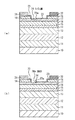
先ず、図1(a)に示すように、バッファ層11、ボトムバリア層12、電子走行層であるチャネル層13、スペーサ層14、Si−δ−ドーピング層15、電子供給層であるバリア層16、i−InP層17、及びキャップ層18を順次形成する。
詳細には、例えば有機金属化学気相成長(MOCVD:Metal Organic Chemical Vapor Deposition)法により、以下の各化合物半導体を成長する。MOVPE法の代わりに、分子線エピタキシー(MBE:Molecular Beam Epitaxy)法等を用いても良い。
First, as shown in FIG. 1A, a
Specifically, the following compound semiconductors are grown by, for example, a metal organic chemical vapor deposition (MOCVD) method. Instead of the MOVPE method, a molecular beam epitaxy (MBE) method or the like may be used.
InP基板10上に、適当なバッファ層を形成し、その上に、i−In0.52Al0.48Asを200nm程度の厚みに成長させる。その上に、i−In0.53Ga0.47Asを10nm程度の厚みに成長させる。その上に、i−In0.52Al0.48Asを3nm程度の厚みに成長させる。次に、極薄に例えば1×10¹³/cm3程度の濃度にSiをドーピングする。その上に、i−In0.52Al0.48Asを6nm程度の厚みに成長させる。その上に、i−InPを3nm程度の厚みに成長させる。その上に、n型不純物、例えばSiを1×1019/cm3程度の濃度にドーピングしたn−In0.53Ga0.47Asを20nm程度の厚みに成長させる。
An appropriate buffer layer is formed on the
以上により、InP基板10上に、バッファ層11、ボトムバリア層12、チャネル層13、スペーサ層14、Si−δ−ドーピング層15、バリア層16、i−InP層17、及びキャップ層18が積層され、化合物半導体積層構造1が形成される。
As described above, the
続いて、素子分離を行った後、図1(b)に示すように、ソース電極31及びドレイン電極32を形成する。
詳細には、先ず、ソース電極及びドレイン電極を形成するためのレジストマスクを形成する。レジストを化合物半導体積層構造1上に塗布し、フォトリソグラフィーにより、化合物半導体積層構造1上の電極形成予定箇所を露出させる開口を形成する。以上により、当該開口を有するレジストマスクが形成される。
Subsequently, after element isolation, a
Specifically, first, a resist mask for forming the source electrode and the drain electrode is formed. A resist is applied onto the compound
このレジストマスクを用いて、電極材料として、例えばTi/Pt/Auを、例えば蒸着法により、化合物半導体積層構造1上の電極形成予定箇所を露出させる開口内を含むレジストマスク上に堆積する。Tiの厚みは10nm程度、Ptの厚みは10nm程度、Auの厚みは200nm程度とする。リフトオフ法により、レジストマスク及びその上に堆積したTi/Pt/Auを除去する。Ti/Pt/Auの場合は、熱処理することなくキャップ層18とのオーミックコンタクトが得られる。以上により、ソース電極31及びドレイン電極32が形成される。
Using this resist mask, for example, Ti / Pt / Au is deposited as an electrode material on the resist mask including the inside of the opening that exposes the electrode formation planned position on the compound
続いて、図2(a)に示すように、SiO2膜21を形成する。
詳細には、化合物半導体積層構造1上のソース電極31とドレイン電極32との間に、絶縁物、ここではSiO2をプラズマCVD法等により20nm程度の厚みに堆積する。以上により、SiO2膜21が形成される。
Subsequently, as shown in FIG. 2A, an SiO 2 film 21 is formed.
Specifically, an insulator, here SiO 2 , is deposited to a thickness of about 20 nm between the
続いて、図2(b)に示すように、レジスト膜22を形成する。
詳細には、SiO2膜21上に、例えば日本ゼオン株式会社製のZEPレジストを塗布する。以上により、レジスト膜22が形成される。
Subsequently, as shown in FIG. 2B, a resist
Specifically, for example, a ZEP resist manufactured by Nippon Zeon Co., Ltd. is applied on the SiO 2 film 21. Thus, the resist
続いて、図3(a)に示すように、SiO2膜21に開口21aを形成する。
詳細には、先ず、電子ビーム露光法等によりレジスト膜22に開口22aを形成する。
次に、レジスト膜22をマスクとして、反応性イオンエッチング法によりSiO2膜21に開口21aを形成する。エッチングガスには例えばCF4を用いる。
その後、レジスト膜22は、薬液処理又はアッシング処理により除去される。
Subsequently, an opening 21 a is formed in the SiO 2 film 21 as shown in FIG.
Specifically, first, an opening 22a is formed in the resist
Next, an
Thereafter, the resist
続いて、図3(b)に示すように、キャップ層18をエッチングする。
詳細には、キャップ層18を電気的に分離するため、キャップ層18をウェットエッチングする。エッチング液には、例えばクエン酸(C6H8O7)と過酸化水素水(H2O2)の混合溶液を用いる。
Subsequently, as shown in FIG. 3B, the
Specifically, the
続いて、図4(a)に示すように、ウェットエッチングにより、残存したSiO2膜21を除去する。 Subsequently, as shown in FIG. 4A, the remaining SiO 2 film 21 is removed by wet etching.
続いて、図4(b)に示すように、SiO2膜23を形成する。
詳細には、化合物半導体積層構造1上のソース電極31とドレイン電極32との間に、絶縁物、ここではSiO2をプラズマCVD法等により堆積する。以上により、SiO2膜23が形成される。
Subsequently, as shown in FIG. 4B, an SiO 2 film 23 is formed.
Specifically, an insulator, here SiO 2 , is deposited between the
続いて、図5(a)に示すように、SiO2膜23に開口23aを形成する。
詳細には、先ず、SiO2膜23上にレジストを塗布し、電子ビーム露光法等によりレジストに開口を形成する。
次に、上記のレジストをマスクとして、反応性イオンエッチング法によりSiO2膜23に開口23aを形成する。エッチングガスには例えばCF4を用いる。開口23aは、ソース電極31寄りに、例えば150nm程度の長さに形成される。
その後、レジストは、薬液処理又はアッシング処理により除去される。
Subsequently, as shown in FIG. 5A, an opening 23 a is formed in the SiO 2 film 23.
Specifically, first, a resist is applied on the SiO 2 film 23, and an opening is formed in the resist by an electron beam exposure method or the like.
Next, an
Thereafter, the resist is removed by a chemical treatment or an ashing treatment.
続いて、図5(b)に示すように、i−InP層17に溝17aを形成する。
詳細には、i−InP層17をウェットエッチングし、深さ1nm〜2nm程度の溝17aを形成する。エッチング液には、例えばクエン酸(C6H8O7)と過酸化水素水(H2O2)の混合溶液を用いる。
Subsequently, as illustrated in FIG. 5B, a groove 17 a is formed in the i-
Specifically, the i-
続いて、図6(a)に示すように、溝17aを埋め込むSiO2膜24を形成する。
詳細には、溝17aを埋め込むように、絶縁物、ここではSiO2をプラズマCVD法等により堆積する。以上により、SiO2膜24が形成される。
Subsequently, as shown in FIG. 6A, an SiO 2 film 24 for filling the groove 17a is formed.
Specifically, an insulator, here SiO 2 , is deposited by plasma CVD or the like so as to fill the groove 17a. Thus, the SiO 2 film 24 is formed.
続いて、図6(b)に示すように、SiO2膜24に開口24aを形成する。
詳細には、先ず、SiO2膜24上にレジストを塗布し、電子ビーム露光法等によりレジストに開口を形成する。
次に、上記のレジストをマスクとして、反応性イオンエッチング法によりSiO2膜24に開口24aを形成する。エッチングガスには例えばCF4を用いる。開口24aは、ソース電極31寄りの端部が開口23aのソース電極31寄りの端部と一致するように、開口23aよりも短く、例えば130nm程度の長さに形成される。
その後、レジストは、薬液処理又はアッシング処理により除去される。
Subsequently, as shown in FIG. 6B, an opening 24 a is formed in the SiO 2 film 24.
Specifically, first, a resist is applied on the SiO 2 film 24, and an opening is formed in the resist by an electron beam exposure method or the like.
Next, using the resist as a mask, an
Thereafter, the resist is removed by a chemical treatment or an ashing treatment.
続いて、図7(a)に示すように、i−InP層17に溝17bを形成する。
詳細には、i−InP層17をウェットエッチングし、深さ1nm〜2nm程度の溝17bを形成する。溝17bは、一部残存した溝17aよりも1nm〜2nm程度深く形成され、溝17a,17b間で段差が形成される。エッチング液には、例えばクエン酸(C6H8O7)と過酸化水素水(H2O2)の混合溶液を用いる。
Subsequently, as shown in FIG. 7A, a groove 17 b is formed in the i-
Specifically, the i-
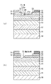
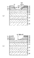
続いて、図7(b)に示すように、階段状溝20を形成する。
詳細には、図6(a)〜図7(a)の各工程を繰り返し、溝を形成してゆく。以上により、化合物半導体積層構造1には、ソース電極31の近傍からゲート電極の形成予定箇所のソース電極側の端部までの領域に、階段状溝20が形成される。階段状溝20は、ソース電極とゲート電極との間に、ソース電極に近づくにつれて逐次階段状に深くなるように、最も深い箇所でバリア層16の途中の深さまで形成される。
Subsequently, as shown in FIG. 7B, stepped
In detail, each process of Drawing 6 (a)-Drawing 7 (a) is repeated, and a slot is formed. As described above, the step-
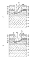
続いて、図8(a)に示すように、SiO2膜25を形成する。
詳細には、化合物半導体積層構造1上のソース電極31とドレイン電極32との間に、階段状溝20を覆うように絶縁物、ここではSiO2をプラズマCVD法等により堆積する。以上により、SiO2膜25が形成される。
Subsequently, as shown in FIG. 8A, an SiO 2 film 25 is formed.
Specifically, an insulator, here SiO 2 , is deposited between the
続いて、図8(b)に示すように、3層のレジスト膜41〜43を積層形成する。
詳細には、化合物半導体積層構造1上を覆うように、例えば日本ゼオン株式会社製のZEPレジスト、PMGI(Poly-dimethylglutarimide)レジスト、及びZEPレジストを塗布する。以上により、レジスト膜41〜43が形成される。
Subsequently, as shown in FIG. 8B, three layers of resist
Specifically, for example, a ZEP resist, a PMGI (Poly-dimethylglutarimide) resist, and a ZEP resist manufactured by Nippon Zeon Co., Ltd. are applied so as to cover the compound
続いて、図9(a)に示すように、レジスト膜42に開口42aを、レジスト膜43に開口43aを形成する。
詳細には、電子ビーム露光法等により、レジスト膜42,43のT型ゲートのヘッド部分が形成される箇所を露光し、レジスト膜42,43に開口42a,43aを形成する。
Subsequently, as shown in FIG. 9A, an opening 42 a is formed in the resist
Specifically, the portions of the resist
続いて、図9(b)に示すように、レジスト膜41に開口41aを形成する。
詳細には、電子ビーム露光法等により、レジスト膜41のT型ゲートのフット部分が形成される箇所を目的とするゲート長に合わせて露光し、レジスト膜41に開口41aを形成する。
Subsequently, as illustrated in FIG. 9B, an opening 41 a is formed in the resist
More specifically, an opening 41 a is formed in the resist
続いて、図10(a)に示すように、SiO2膜25に開口25aを形成する。
詳細には、レジスト膜41をマスクとして、反応性イオンエッチング法によりSiO2膜25に開口25aを形成する。エッチングガスには例えばCF4を用いる。
Subsequently, as shown in FIG. 10A, an opening 25 a is formed in the SiO 2 film 25.
More specifically, the
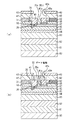
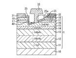
続いて、図10(b)及び図11に示すように、ゲート電極33を形成する。
詳細には、レジスト膜41〜43をマスクとして用いて、電極材料として、例えばTi/Pt/Auを、例えば蒸着法により、開口41a〜43a内を含むレジスト膜43上に堆積する。Tiの厚みは10nm程度、Ptの厚みは5nm程度、Auの厚みは400nm程度とする。リフトオフ法により、レジスト膜41〜43及びレジスト膜43上に堆積されたTi/Pt/Auを除去する。以上により、図11に示すように、i−InP17上にT型のゲート電極33が形成される。
以上により、本実施形態によるInAlAs/InGaAs系HEMTが形成される。
Subsequently, as shown in FIGS. 10B and 11, a
Specifically, using the resist
As described above, the InAlAs / InGaAs-based HEMT according to the present embodiment is formed.
本実施形態では、ゲート電極33が化合物半導体積層構造1と直接的に接触する、ショットキー型のInAlAs/InGaAs系HEMTを作製する場合を例示した。ショットキー型の代わりに、ゲート電極33がゲート絶縁膜を介して化合物半導体積層構造1の上方に形成されるMIS型のInAlAs/InGaAs系HEMTを形成するようにしても良い。この場合、図9(b)の工程の後に、SiO2膜25に開口25aを形成する図10(a)の工程を行わず、図10(b)以降の工程を行うようにすれば良い。
In the present embodiment, the case where a Schottky type InAlAs / InGaAs-based HEMT in which the
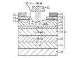
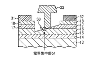
本実施形態のInAlAs/InGaAs系HEMTでは、図11のようにソース電極31とゲート電極33との間に、ソース電極31に近づくにつれて逐次階段状に深くなる階段状溝20を形成する場合を例示した。階段状溝20の段差が小さくなるように、段差形成をすれば、階段状溝20は連続的な傾斜溝と見なせるようになる。現実的には、化合物半導体の1原子層分の高さが当該段差の限界となる。本実施形態のInAlAs/InGaAs系HEMTとして、連続的と見なせる傾斜溝、即ち、ソース電極31とゲート電極33との間に、ソース電極31に近づくにつれて徐々に深くなるテーパ状溝30が形成されたものを図12に示す。図12においては、SiO2膜25の記載を省略している。本実施形態では、以降、本実施形態のInAlAs/InGaAs系HEMTをテーパ状溝30が形成されたものとして、その作用効果等を説明する。
In the InAlAs / InGaAs-based HEMT of this embodiment, as shown in FIG. 11, an example is shown in which a stepped
図13は、本実施形態のInAlAs/InGaAs系HEMTにおいて、ソース電極31に近い領域とゲート電極33に近い領域における垂直方向の伝導帯のバンド構造を示す模式図である。
ソース電極31寄りからゲート電極33寄りに近づくにつれて、チャネル層13の伝導帯の底のエネルギーが下がり、ソース電極31−ゲート電極33間に内部電界が形成されていることが判る。これは、テーパ状溝30の形成により、ソース電極31に近づくほどバリア層16が薄くなるため、全体にポテンシャルが持ち上げられるためである。
FIG. 13 is a schematic diagram showing the band structure of the conduction band in the vertical direction in the region close to the
As the distance from the
図14は、本実施形態のInAlAs/InGaAs系HEMTにおいて、ポテンシャルの変化を説明するための模式図であり、(a)が概略断面図、(b)が比較例との比較に基づいて、チャネル層内の伝導帯バンド構造を示す特性図である。比較例としては、化合物半導体積層構造にテーパ状溝30が形成されておらず表面平坦である従来のInAlAs/InGaAs系HEMTを例示する。
FIG. 14 is a schematic diagram for explaining a potential change in the InAlAs / InGaAs-based HEMT of this embodiment, where (a) is a schematic cross-sectional view, and (b) is a channel based on a comparison with a comparative example. It is a characteristic view which shows the conduction band structure in a layer. As a comparative example, a conventional InAlAs / InGaAs-based HEMT in which the tapered
ドレイン電圧は印加状態とされており、チャネル層13内の電子は、ソース電極31からドレイン電極32へ流れている。本実施形態では、図14(a)のように、化合物半導体積層構造1にテーパ状溝30を形成する(図14(a)の円内)。これにより、図14(b)のように、ソース電極31−ゲート電極33間の矢印Aに沿ったポテンシャルが減少し、内部電界が生成してソース抵抗が下がる。
The drain voltage is in an applied state, and electrons in the
以上のように、ソース電極31とゲート電極33との領域に、ソース電極31に近づくにつれて逐次階段状に深くなるテーパ状溝30を有することにより、当該領域において内部電界が生成される。これにより、ソース電極31−ゲート電極33間の電子が比較例の場合よりも加速し易くなる。ドレイン電流Idsは、
Ids=nev(n:電子密度、e:単位電荷,v:電子速度)
で表される。電子密度nは、n型オーミックコンタクト部分から電子が供給され、この部分は本実施形態でも比較例でも同程度である。これに対して、電子速度vは内部電界により増大する。比較例よりもドレイン電流が流れ易くなり、ソース抵抗が低減される。
As described above, by having the tapered
I ds = nev (n: electron density, e: unit charge, v: electron velocity)
It is represented by The electron density n is supplied with electrons from the n-type ohmic contact portion, and this portion is comparable in this embodiment and the comparative example. On the other hand, the electron velocity v increases due to the internal electric field. The drain current can flow more easily than the comparative example, and the source resistance is reduced.
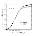
図15は、シミュレーションの対象とした本実施形態のInAlAs/InGaAs系HEMTを示す概略断面図である。図16は、本実施形態のInAlAs/InGaAs系HEMTのドレイン電流Ids−ゲート電圧Vgs特性について、比較例との比較に基づいて調べたシミュレーション結果を示す特性図である。図17は、本実施形態のInAlAs/InGaAs系HEMTの相互コンダクタンスgmのゲート電圧Vgs依存性について、比較例との比較に基づいて調べたシミュレーション結果を示す特性図である。 FIG. 15 is a schematic cross-sectional view showing the InAlAs / InGaAs-based HEMT according to the present embodiment, which is a simulation target. FIG. 16 is a characteristic diagram showing a simulation result obtained by examining the drain current I ds -gate voltage V gs characteristic of the InAlAs / InGaAs-based HEMT according to the present embodiment based on a comparison with a comparative example. FIG. 17 is a characteristic diagram showing a simulation result obtained by examining the dependence of the mutual conductance g m on the gate voltage V gs of the InAlAs / InGaAs-based HEMT of this embodiment on the basis of comparison with a comparative example.
化合物半導体積層構造のソース電極とゲート電極と間が平坦な比較例では、最大相互コンダクタンスgmは0.496(S/mm)である。化合物半導体積層構造1のソース電極31とゲート電極33と間にテーパ状溝30を形成した本実施形態では、最大相互コンダクタンスgmは0.533(S/mm)となり、比較例よりも増大している。以上のように、テーパ状溝30の存在により、最大ドレイン電流及び最大相互コンダクタンスが増大しており、本実施形態の有効性が確認された。
In the comparative example in which the distance between the source electrode and the gate electrode of the compound semiconductor multilayer structure is flat, the maximum transconductance g m is 0.496 (S / mm). In this embodiment in which the tapered
以上説明したように、本実施形態によれば、ソース抵抗を低減し、動作速度を向上させることができる信頼性の高いInAlAs/InGaAs系HEMTが実現する。 As described above, according to the present embodiment, a highly reliable InAlAs / InGaAs-based HEMT capable of reducing the source resistance and improving the operation speed is realized.
(第1の実施形態の変形例)
以下、本実施形態の変形例による様々なHEMTについて説明する。
(Modification of the first embodiment)
Hereinafter, various HEMTs according to modifications of the present embodiment will be described.
−変形例1−
変形例1では、AlGaAs/GaAs系HEMTを開示する。
図18は、変形例1によるAlGaAs/GaAs系HEMTを示す概略断面図である。
-Modification 1-
In
FIG. 18 is a schematic sectional view showing an AlGaAs / GaAs HEMT according to the first modification.
このAlGaAs/GaAs系HEMTでは、基板100上に、バッファ層101、ボトムバリア層102、チャネル層103、スペーサ層104、Si−δ−ドーピング層105、バリア層106、及びキャップ層107が順次積層されている。
ボトムバリア層102は、i−AlGaAs(例えば、i−Al0.3Ga0.7As)が成長されて形成される。チャネル層103は、i−GaAsが成長されて形成される。スペーサ層104は、i−AlGaAs(例えば、i−Al0.3Ga0.7As)が成長されて形成される。Si−δ−ドーピング層105は、極薄のSiドーピングで形成される。バリア層106は、i−AlGaAs(例えば、i−Al0.3Ga0.7As)が成長されて形成される。キャップ層107は、n−GaAsが成長されて形成される。
In this AlGaAs / GaAs HEMT, a buffer layer 101, a bottom barrier layer 102, a channel layer 103, a spacer layer 104, a Si-δ-doping layer 105, a barrier layer 106, and a
The bottom barrier layer 102 is formed by growing i-AlGaAs (for example, i-Al 0.3 Ga 0.7 As). The channel layer 103 is formed by growing i-GaAs. The spacer layer 104 is formed by growing i-AlGaAs (for example, i-Al 0.3 Ga 0.7 As). The Si-δ-doping layer 105 is formed by extremely thin Si doping. The barrier layer 106 is formed by growing i-AlGaAs (for example, i-Al 0.3 Ga 0.7 As). The
キャップ層107上にはソース電極31及びドレイン電極32が形成され、バリア層106上にはゲート電極33が形成される。ソース電極31とゲート電極33との間に、ソース電極31に近づくにつれて徐々に深くなるテーパ状溝30が形成される。テーパ状溝30は、最も深い箇所でバリア層106の途中の深さまで形成される。
A
本例では、ソース抵抗を低減し、動作速度を向上させることができる信頼性の高いAlGaAs/GaAs系HEMTが実現する。 In this example, a highly reliable AlGaAs / GaAs HEMT capable of reducing the source resistance and improving the operation speed is realized.
−変形例2−
変形例2では、AlGaAs/InGaAs系HEMTを開示する。
図19は、変形例2によるAlGaAs/InGaAs系HEMTを示す概略断面図である。
-Modification 2-
In Modification 2, an AlGaAs / InGaAs HEMT is disclosed.
FIG. 19 is a schematic cross-sectional view showing an AlGaAs / InGaAs HEMT according to the second modification.
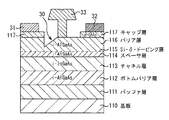
このAlGaAs/InGaAs系HEMTでは、基板110上に、バッファ層111、ボトムバリア層112、チャネル層113、スペーサ層114、Si−δ−ドーピング層115、バリア層116、及びキャップ層117が順次積層されている。
ボトムバリア層112は、i−AlGaAs(例えば、i−Al0.3Ga0.7As)が成長されて形成される。チャネル層113は、i−InGaAsが成長されて形成される。スペーサ層114は、i−AlGaAs(例えば、i−Al0.3Ga0.7As)が成長されて形成される。Si−δ−ドーピング層115は、極薄のSiドーピングで形成される。バリア層116は、i−AlGaAs(例えば、i−Al0.3Ga0.7As)が成長されて形成される。キャップ層117は、n−GaAsが成長されて形成される。
In this AlGaAs / InGaAs HEMT, a buffer layer 111, a bottom barrier layer 112, a channel layer 113, a spacer layer 114, a Si-δ-doping layer 115, a barrier layer 116, and a cap layer 117 are sequentially stacked on a substrate 110. ing.
The bottom barrier layer 112 is formed by growing i-AlGaAs (for example, i-Al 0.3 Ga 0.7 As). The channel layer 113 is formed by growing i-InGaAs. The spacer layer 114 is formed by growing i-AlGaAs (for example, i-Al 0.3 Ga 0.7 As). The Si-δ-doping layer 115 is formed by extremely thin Si doping. The barrier layer 116 is formed by growing i-AlGaAs (for example, i-Al 0.3 Ga 0.7 As). The cap layer 117 is formed by growing n-GaAs.
キャップ層117上にはソース電極31及びドレイン電極32が形成され、バリア層116上にはゲート電極33が形成される。ソース電極31とゲート電極33との間に、ソース電極31に近づくにつれて徐々に深くなるテーパ状溝30が形成される。テーパ状溝30は、最も深い箇所でバリア層116の途中の深さまで形成される。
A
本例では、ソース抵抗を低減し、動作速度を向上させることができる信頼性の高いAlGaAs/InGaAs系HEMTが実現する。 In this example, a highly reliable AlGaAs / InGaAs HEMT capable of reducing the source resistance and improving the operation speed is realized.
−変形例3−
変形例3では、AlSb/InAs系HEMTを開示する。
図20は、変形例3によるAlSb/InAs系HEMTを示す概略断面図である。
-Modification 3-
Modification 3 discloses an AlSb / InAs HEMT.
FIG. 20 is a schematic cross-sectional view showing an AlSb / InAs-based HEMT according to Modification 3.
このAlSb/InAs系HEMTでは、基板120上に、バッファ層121、ボトムバリア層122、チャネル層123、スペーサ層124、Te−δ−ドーピング層125、バリア層126、i−InAlAs層127、及びキャップ層128が順次積層されている。
ボトムバリア層122は、i−AlSbが成長されて形成される。チャネル層123は、i−InAsが成長されて形成される。スペーサ層124は、i−AlSbが成長されて形成される。Te−δ−ドーピング層125は、極薄のTeドーピングで形成される。バリア層126は、i−AlSbが成長されて形成される。i−InAlAs層127は、例えばi−In0.5Al0.5Asが成長されて形成される。キャップ層128は、n−InAsが成長されて形成される。
In this AlSb / InAs HEMT, a buffer layer 121, a bottom barrier layer 122, a channel layer 123, a
The bottom barrier layer 122 is formed by growing i-AlSb. The channel layer 123 is formed by growing i-InAs. The
キャップ層128上にはソース電極31及びドレイン電極32が形成され、i−InAlAs層127上にはゲート電極33が形成される。ソース電極31とゲート電極33との間に、ソース電極31に近づくにつれて徐々に深くなるテーパ状溝30が形成される。テーパ状溝30は、最も深い箇所でバリア層126の途中の深さまで形成される。
A
本例では、ソース抵抗を低減し、動作速度を向上させることができる信頼性の高いAlSb/InAs系HEMTが実現する。 In this example, a highly reliable AlSb / InAs-based HEMT capable of reducing the source resistance and improving the operation speed is realized.
−変形例4−
変形例4では、InAlSb/InSb系HEMTを開示する。
図21は、変形例4によるInAlSb/InSb系HEMTを示す概略断面図である。
-Modification 4-
In Modification 4, an InAlSb / InSb-based HEMT is disclosed.
FIG. 21 is a schematic cross-sectional view showing an InAlSb / InSb-based HEMT according to Modification 4.
このInAlSb/InSb系HEMTでは、基板130上に、バッファ層131、ボトムバリア層132、チャネル層133、スペーサ層134、Te−δ−ドーピング層135、バリア層136、及びキャップ層137が順次積層されている。
ボトムバリア層132は、i−InAlSbが成長されて形成される。チャネル層133は、i−InSbが成長されて形成される。スペーサ層134は、i−InAlSb(例えば、i−In0.75Al0.25Sb)が成長されて形成される。Te−δ−ドーピング層135は、極薄のTeドーピングで形成される。バリア層136は、i−InAlSb(例えば、i−In0.75Al0.25Sb)が成長されて形成される。キャップ層137は、n−InSbが成長されて形成される。
In this InAlSb / InSb-based HEMT, a
The bottom barrier layer 132 is formed by growing i-InAlSb. The channel layer 133 is formed by growing i-InSb. The spacer layer 134 is formed by growing i-InAlSb (for example, i-In 0.75 Al 0.25 Sb). The Te-δ-doping layer 135 is formed by extremely thin Te doping. The barrier layer 136 is formed by growing i-InAlSb (for example, i-In 0.75 Al 0.25 Sb). The
キャップ層137上にはソース電極31及びドレイン電極32が形成され、バリア層136上にはゲート電極33が形成される。ソース電極31とゲート電極33との間に、ソース電極31に近づくにつれて徐々に深くなるテーパ状溝30が形成される。テーパ状溝30は、最も深い箇所でバリア層137の途中の深さまで形成される。
A
本例では、ソース抵抗を低減し、動作速度を向上させることができる信頼性の高いInAlSb/InSb系HEMTが実現する。 In this example, a highly reliable InAlSb / InSb-based HEMT capable of reducing the source resistance and improving the operation speed is realized.
−変形例5−
変形例5では、AlGaN/GaN系HEMTを開示する。
図22は、変形例5によるAlGaN/GaN系HEMTを示す概略断面図である。
-Modification 5-
In Modification 5, an AlGaN / GaN-based HEMT is disclosed.
FIG. 22 is a schematic cross-sectional view showing an AlGaN / GaN-based HEMT according to Modification 5.
このAlGaN/GaN系HEMTでは、基板140上に、バッファ層141、チャネル層142、スペーサ層143、及びバリア層144が順次積層されている。
チャネル層142は、i−GaNが成長されて形成される。スペーサ層143は、i−AlNが成長されて形成される。バリア層144は、i−AlGaN(例えば、i−Al0.3Ga0.7N)が成長されて形成される。
In this AlGaN / GaN-based HEMT, a buffer layer 141, a channel layer 142, a spacer layer 143, and a barrier layer 144 are sequentially stacked on a substrate 140.
The channel layer 142 is formed by growing i-GaN. The spacer layer 143 is formed by growing i-AlN. The barrier layer 144 is formed by growing i-AlGaN (for example, i-Al 0.3 Ga 0.7 N).
バリア層144上には、ゲート電極33及びこれを挟むソース電極31及びドレイン電極32が形成される。ソース電極31とゲート電極33との間に、ソース電極31に近づくにつれて徐々に深くなるテーパ状溝30が形成される。テーパ状溝30は、最も深い箇所でバリア層144の途中の深さまで形成される。
On the barrier layer 144, the
本例では、ソース抵抗を低減し、動作速度を向上させることができる信頼性の高いAlGaN/GaN系HEMTが実現する。 In this example, a highly reliable AlGaN / GaN HEMT capable of reducing the source resistance and improving the operation speed is realized.
−変形例6−
変形例6では、InAlN/GaN系HEMTを開示する。
図23は、変形例6によるInAlN/GaN系HEMTを示す概略断面図である。
-Modification 6
In Modification 6, an InAlN / GaN-based HEMT is disclosed.
FIG. 23 is a schematic cross-sectional view showing an InAlN / GaN-based HEMT according to Modification 6.
このInAlN/GaN系HEMTでは、基板150上に、バッファ層151、チャネル層152、スペーサ層153、及びバリア層154が順次積層されている。
チャネル層152は、i−GaNが成長されて形成される。スペーサ層153は、i−AlNが成長されて形成される。バリア層154は、i−InAlNが成長されて形成される。
In this InAlN / GaN-based HEMT, a buffer layer 151, a channel layer 152, a spacer layer 153, and a barrier layer 154 are sequentially stacked on a substrate 150.
The channel layer 152 is formed by growing i-GaN. The spacer layer 153 is formed by growing i-AlN. The barrier layer 154 is formed by growing i-InAlN.
バリア層154上には、ゲート電極33及びこれを挟むソース電極31及びドレイン電極32が形成される。ソース電極31とゲート電極33との間に、ソース電極31に近づくにつれて徐々に深くなるテーパ状溝30が形成される。テーパ状溝30は、最も深い箇所でバリア層154の途中の深さまで形成される。
On the barrier layer 154, the
本例では、ソース抵抗を低減し、動作速度を向上させることができる信頼性の高いInAlN/GaN系HEMTが実現する。 In this example, a highly reliable InAlN / GaN-based HEMT capable of reducing the source resistance and improving the operation speed is realized.
−変形例7−
変形例7では、SiGe/Si系HEMTを開示する。
図24は、変形例7によるSiGe/Si系HEMTを示す概略断面図である。
-Modification 7-
In Modification 7, a SiGe / Si-based HEMT is disclosed.
FIG. 24 is a schematic cross-sectional view showing a SiGe / Si-based HEMT according to Modification 7.
このSiGe/Si系HEMTでは、基板160上に、バッファ層161、ボトムバリア層162、チャネル層163、スペーサ層164、バリア層165、i−Si層166,及びキャップ層167が順次積層されている。
ボトムバリア層162は、i−SiGeが形成される。チャネル層163は、i−Siが形成される。スペーサ層164は、i−SiGeが形成される。バリア層165は、n−SiGeが形成される。キャップ層167は、n−Siが形成される。
In this SiGe / Si-based HEMT, a buffer layer 161, a bottom barrier layer 162, a channel layer 163, a spacer layer 164, a barrier layer 165, an i-
The bottom barrier layer 162 is formed with i-SiGe. The channel layer 163 is formed with i-Si. The spacer layer 164 is formed of i-SiGe. The barrier layer 165 is formed of n-SiGe. The cap layer 167 is formed with n-Si.
キャップ層167上にはソース電極31及びドレイン電極32が形成され、i−Si層166上にはゲート電極33が形成される。ソース電極31とゲート電極33との間に、ソース電極31に近づくにつれて徐々に深くなるテーパ状溝30が形成される。テーパ状溝30は、最も深い箇所でバリア層165の途中の深さまで形成される。
A
本例では、ソース抵抗を低減し、動作速度を向上させることができる信頼性の高いSiGe/Si系HEMTが実現する。 In this example, a highly reliable SiGe / Si-based HEMT capable of reducing the source resistance and improving the operation speed is realized.
(第2の実施形態)
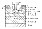
本実施形態では、第1の実施形態と同様に、InAlAs/InGaAs系HEMTを開示するが、そのテーパ状溝(階段状溝)の形成箇所が若干異なる点で第1の実施形態と相違する。
図25〜図31は、第2の実施形態によるInAlAs/InGaAs系HEMTの製造方法の主要工程を示す概略断面図である。
(Second Embodiment)
In this embodiment, an InAlAs / InGaAs-based HEMT is disclosed as in the first embodiment, but is different from the first embodiment in that the tapered groove (step groove) is slightly different.
FIG. 25 to FIG. 31 are schematic cross-sectional views showing the main steps of the method of manufacturing the InAlAs / InGaAs-based HEMT according to the second embodiment.
先ず、第1の実施形態と同様に、図1(a)〜図4(b)の各工程を行う。
続いて、図25(a)に示すように、SiO2膜23に開口23Aを形成する。
詳細には、先ず、SiO2膜23上にレジストを塗布し、電子ビーム露光法等によりレジストに開口を形成する。
次に、上記のレジストをマスクとして、反応性イオンエッチング法によりSiO2膜23に開口23Aを形成する。エッチングガスには例えばCF4を用いる。開口23Aは、ソース電極31とドレイン電極32との間に亘る領域に、例えば180nm程度の長さに形成される。
その後、レジストは、薬液処理又はアッシング処理により除去される。
First, similarly to the first embodiment, each step of FIG. 1A to FIG. 4B is performed.
Subsequently, an
Specifically, first, a resist is applied on the SiO 2 film 23, and an opening is formed in the resist by an electron beam exposure method or the like.
Next, an
Thereafter, the resist is removed by a chemical treatment or an ashing treatment.
続いて、図25(b)に示すように、i−InP層17に溝17Aを形成する。
詳細には、i−InP層17をウェットエッチングし、深さ1nm〜2nm程度の溝17Aを形成する。エッチング液には、例えばクエン酸(C6H8O7)と過酸化水素水(H2O2)の混合溶液を用いる。
Subsequently, as illustrated in FIG. 25B, a
Specifically, the i-
続いて、図26(a)に示すように、溝17Aを埋め込むSiO2膜24を形成する。
詳細には、溝17Aを埋め込むように、絶縁物、ここではSiO2をプラズマCVD法等により堆積する。以上により、SiO2膜24が形成される。
Subsequently, as shown in FIG. 26A, an SiO 2 film 24 for embedding the groove 17A is formed.
Specifically, an insulator, here SiO 2 , is deposited by plasma CVD or the like so as to fill the groove 17A. Thus, the SiO 2 film 24 is formed.
続いて、図26(b)に示すように、SiO2膜24に開口24Aを形成する。
詳細には、先ず、SiO2膜24上にレジストを塗布し、電子ビーム露光法等によりレジストに開口を形成する。
次に、上記のレジストをマスクとして、反応性イオンエッチング法によりSiO2膜24に開口24Aを形成する。エッチングガスには例えばCF4を用いる。開口24Aは、ソース電極31寄りの端部が開口23Aのソース電極31寄りの端部と一致するように、開口23Aよりも短く、例えば170nm程度の長さに形成される。
その後、レジストは、薬液処理又はアッシング処理により除去される。
Subsequently, an
Specifically, first, a resist is applied on the SiO 2 film 24, and an opening is formed in the resist by an electron beam exposure method or the like.
Next, an
Thereafter, the resist is removed by a chemical treatment or an ashing treatment.
続いて、図27(a)に示すように、i−InP層17に溝17Bを形成する。
詳細には、i−InP層17をウェットエッチングし、深さ1nm〜2nm程度の溝17Bを形成する。溝17bは、一部残存した溝17Aよりも1nm〜2nm程度深く形成され、溝17A,17B間で段差が形成される。エッチング液には、例えばクエン酸(C6H8O7)と過酸化水素水(H2O2)の混合溶液を用いる。
Subsequently, as illustrated in FIG. 27A, a
Specifically, the i-
続いて、図27(b)に示すように、階段状溝40を形成する。
詳細には、図26(a)〜図27(a)の各工程を繰り返し、溝を形成してゆく。以上により、化合物半導体積層構造1には、ソース電極31の近傍からドレイン電極32の近傍までの領域に、階段状溝40が形成される。階段状溝40は、ソース電極31とドレイン電極32との間に、ソース電極31に近づくにつれて逐次階段状に深くなるように、最も深い箇所でバリア層16の途中の深さまで形成される。
Subsequently, as shown in FIG. 27B, stepped
Specifically, the steps shown in FIGS. 26A to 27A are repeated to form grooves. As described above, the stepped
続いて、図28(a)に示すように、SiO2膜25を形成する。
詳細には、化合物半導体積層構造1上のソース電極31とドレイン電極32との間に、階段状溝40を覆うように絶縁物、ここではSiO2をプラズマCVD法等により堆積する。以上により、SiO2膜25が形成される。
Subsequently, as shown in FIG. 28A, an SiO 2 film 25 is formed.
Specifically, an insulator, here SiO 2 , is deposited between the
続いて、図28(b)に示すように、3層のレジスト膜41〜43を積層形成する。
詳細には、化合物半導体積層構造1上を覆うように、例えば日本ゼオン株式会社製のZEPレジスト、PMGI(poly-dimethylglutarimide)レジスト、及びZEPレジストを塗布する。以上により、レジスト膜41〜43が形成される。
Subsequently, as shown in FIG. 28B, three layers of resist
Specifically, for example, a ZEP resist, a PMGI (poly-dimethylglutarimide) resist, and a ZEP resist manufactured by Zeon Corporation are applied so as to cover the compound
続いて、図29(a)に示すように、レジスト膜42に開口42aを、レジスト膜43に開口43aを形成する。
詳細には、電子ビーム露光法等により、レジスト膜42,43のT型ゲートのヘッド部分が形成される箇所を露光し、レジスト膜42,43に開口42a,43aを形成する。
Subsequently, as illustrated in FIG. 29A, an opening 42 a is formed in the resist
Specifically, the portions of the resist
続いて、図29(b)に示すように、レジスト膜41に開口41aを形成する。
詳細には、電子ビーム露光法等により、レジスト膜41のT型ゲートのフット部分が形成される箇所を目的とするゲート長に合わせて露光し、レジスト膜41に開口41aを形成する。
Subsequently, as shown in FIG. 29B, an opening 41 a is formed in the resist
More specifically, an opening 41 a is formed in the resist
続いて、図30(a)に示すように、SiO2膜25に開口25aを形成する。
詳細には、レジスト膜41をマスクとして、反応性イオンエッチング法によりSiO2膜25に開口25aを形成する。エッチングガスには例えばCF4を用いる。
Subsequently, as illustrated in FIG. 30A, an opening 25 a is formed in the SiO 2 film 25.
More specifically, the
続いて、図30(b)及び図31に示すように、ゲート電極33を形成する。
詳細には、レジスト膜41〜43をマスクとして用いて、電極材料として、例えばTi/Pt/Auを、例えば蒸着法により、開口41a〜43a内を含むレジスト膜43上に堆積する。Tiの厚みは10nm程度、Ptの厚みは5nm程度、Auの厚みは400nm程度とする。リフトオフ法により、レジスト膜41〜43及びレジスト膜43上に堆積されたTi/Pt/Auを除去する。以上により、図11に示すように、階段状溝40の底面上にT型のゲート電極33が形成される。
以上により、本実施形態によるInAlAs/InGaAs系HEMTが形成される。
Subsequently, as shown in FIGS. 30B and 31, a
Specifically, using the resist
As described above, the InAlAs / InGaAs-based HEMT according to the present embodiment is formed.
本実施形態では、ゲート電極33が化合物半導体積層構造1の階段状溝40の底面と直接的に接触する、ショットキー型のInAlAs/InGaAs系HEMTを作製する場合を例示した。ショットキー型の代わりに、ゲート電極33がゲート絶縁膜を介して化合物半導体積層構造1の上方に形成されるMIS型のInAlAs/InGaAs系HEMTを形成するようにしても良い。この場合、図29(b)の工程の後に、SiO2膜25に開口25aを形成する図30(a)の工程を行わず、図30(b)以降の工程を行うようにすれば良い。
In the present embodiment, the case where a Schottky type InAlAs / InGaAs-based HEMT in which the
本実施形態のInAlAs/InGaAs系HEMTでは、図31のようにソース電極31とドレイン電極32との間に、ソース電極31に近づくにつれて逐次階段状に深くなる階段状溝40を形成する場合を例示した。階段状溝40の段差が小さくなるように、段差形成をすれば、階段状溝40は連続的な傾斜溝と見なせるようになる。現実的には、化合物半導体の1原子層分の高さが当該段差の限界となる。本実施形態のInAlAs/InGaAs系HEMTとして、連続的と見なせる傾斜溝、即ち、ソース電極31とドレイン電極32との間に、ソース電極31に近づくにつれて徐々に深くなるテーパ状溝50が形成されたものを図32に示す。図32においては、SiO2膜25の記載を省略している。本実施形態では、以降、本実施形態のInAlAs/InGaAs系HEMTをテーパ状溝50が形成されたものとして、その作用効果等を説明する。
In the InAlAs / InGaAs-based HEMT of this embodiment, as shown in FIG. 31, an example is shown in which a stepped
図33は、ソース電極31寄りのテーパ状溝50の端部、テーパ状溝50の中央(ゲート電極形成部分、電極形成前)、ドレイン電極32寄りのテーパ状溝50の端部における縦方向の伝導帯のバンド構造を示す模式図である。ソース電極31寄りからドレイン電極32寄りに近づくにつれて、チャネル層13の伝導帯の底のエネルギーが下がり、ソース31−ゲート電極33間に内部電界が形成されていることが判る。これは、ソース電極31に近づくほどバリア層16が薄くなるため、全体にポテンシャルが持ち上げられるためである。このバンド構造図はゲート電極33を形成する前のものであるが、ゲート電極33の形成後もソース31−ゲート電極33間のテーパ状溝50とゲート電極33−ドレイン電極32間のテーパ状溝50とには、両方とも内部電界が形成されている。但し、ゲート電極33−ドレイン電極32間では横方向のリセス長による電界強度への影響が大きいので、ソース31−ゲート電極33間の方が効果は大きい。
FIG. 33 shows the longitudinal direction at the end of the tapered
更に本実施形態では、図34に示すように、ゲート電極33がテーパ状溝50の底面上に形成される。そのため、ゲート電極33のフット先端部分(図34の円内)は、テーパ状溝50の形状に対応して、ソース電極31側がチャネル層13に近い先端が尖った構造になる。本実施形態では、当該構造を有しない(ゲート電極が平坦面上に形成された場合)HEMTに比べて、先端が尖った部分に電界が集中し易くなる。結果として、実効的なゲート長が短くなり真性遅延時間τintも短縮される。
Furthermore, in the present embodiment, the
以上のように、ソース電極31とゲート電極33との領域に、ソース電極31に近づくにつれて逐次階段状に深くなるテーパ状溝50を有することにより、当該領域において内部電界が生成される。これにより、ソース電極31−ゲート電極33間の電子が比較例の場合よりも加速し易くなる。ドレイン電流Idsは、
Ids=nev(n:電子密度、e:単位電荷,v:電子速度)
で表される。電子密度nは、n型オーミックコンタクト部分から電子が供給され、この部分は本実施形態でも比較例でも同程度である。これに対して、電子速度vは内部電界により増大する。比較例よりもドレイン電流が流れ易くなり、ソース抵抗が低減される。
更に本実施形態では、ゲート電極33の底面がテーパ状溝50の底面上に形成されるため、実効的なゲート長が短くなり真性遅延時間τintも短縮される。
As described above, by having the tapered
I ds = nev (n: electron density, e: unit charge, v: electron velocity)
It is represented by The electron density n is supplied with electrons from the n-type ohmic contact portion, and this portion is comparable in this embodiment and the comparative example. On the other hand, the electron velocity v increases due to the internal electric field. The drain current can flow more easily than the comparative example, and the source resistance is reduced.
Furthermore, in this embodiment, since the bottom surface of the
本実施形態によるInAlAs/InGaAs系HEMTでは、真性遅延時間τintと外因性(寄生)遅延時間τextとの両方を低減することが可能である。
以上説明したように、本実施形態によれば、ソース抵抗を低減し、動作速度を向上させることができる信頼性の高いInAlAs/InGaAs系HEMTが実現する。
In the InAlAs / InGaAs HEMT according to the present embodiment, both the intrinsic delay time τ int and the extrinsic (parasitic) delay time τ ext can be reduced.
As described above, according to the present embodiment, a highly reliable InAlAs / InGaAs-based HEMT capable of reducing the source resistance and improving the operation speed is realized.
(第2の実施形態の変形例)
以下、本実施形態の変形例による様々なHEMTについて説明する。
(Modification of the second embodiment)
Hereinafter, various HEMTs according to modifications of the present embodiment will be described.
−変形例1−
変形例1では、AlGaAs/GaAs系HEMTを開示する。
図35は、変形例1によるAlGaAs/GaAs系HEMTを示す概略断面図である。
-Modification 1-
In
FIG. 35 is a schematic sectional view showing an AlGaAs / GaAs HEMT according to the first modification.
このAlGaAs/GaAs系HEMTでは、基板200上に、バッファ層201、ボトムバリア層202、チャネル層203、スペーサ層204、Si−δ−ドーピング層205、バリア層206、及びキャップ層207が順次積層されている。
ボトムバリア層202は、i−AlGaAs(例えば、i−Al0.3Ga0.7As)が成長されて形成される。チャネル層203は、i−GaAsが成長されて形成される。スペーサ層204は、i−AlGaAs(例えば、i−Al0.3Ga0.7As)が成長されて形成される。Si−δ−ドーピング層205は、極薄のSiドーピングで形成される。バリア層206は、i−AlGaAs(例えば、i−Al0.3Ga0.7As)が成長されて形成される。キャップ層207は、n−GaAsが成長されて形成される。
In this AlGaAs / GaAs HEMT, a buffer layer 201, a bottom barrier layer 202, a channel layer 203, a spacer layer 204, an Si-δ-doping layer 205, a barrier layer 206, and a
The bottom barrier layer 202 is formed by growing i-AlGaAs (for example, i-Al 0.3 Ga 0.7 As). The channel layer 203 is formed by growing i-GaAs. The spacer layer 204 is formed by growing i-AlGaAs (for example, i-Al 0.3 Ga 0.7 As). The Si-δ-doping layer 205 is formed by ultra-thin Si doping. The barrier layer 206 is formed by growing i-AlGaAs (for example, i-Al 0.3 Ga 0.7 As). The
キャップ層207上にはソース電極31及びドレイン電極32が形成され、テーパ状溝50の底面上にはゲート電極33が形成される。テーパ状溝50は、ソース電極31とドレイン電極32との間に、ソース電極31に近づくにつれて徐々に深くなるように形成される。テーパ状溝50は、最も深い箇所でバリア層206の途中の深さまで形成される。
A
本例では、ソース抵抗を低減し、動作速度を向上させることができる信頼性の高いAlGaAs/GaAs系HEMTが実現する。 In this example, a highly reliable AlGaAs / GaAs HEMT capable of reducing the source resistance and improving the operation speed is realized.
−変形例2−
変形例2では、AlGaAs/InGaAs系HEMTを開示する。
図36は、変形例2によるAlGaAs/InGaAs系HEMTを示す概略断面図である。
-Modification 2-
In Modification 2, an AlGaAs / InGaAs HEMT is disclosed.
FIG. 36 is a schematic sectional view showing an AlGaAs / InGaAs HEMT according to the second modification.
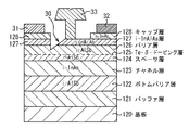
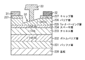
このAlGaAs/InGaAs系HEMTでは、基板210上に、バッファ層211、ボトムバリア層212、チャネル層213、スペーサ層214、Si−δ−ドーピング層215、バリア層216、及びキャップ層217が順次積層されている。
ボトムバリア層212は、i−AlGaAs(例えば、i−Al0.3Ga0.7As)が成長されて形成される。チャネル層213は、i−InGaAsが成長されて形成される。スペーサ層214は、i−AlGaAs(例えば、i−Al0.3Ga0.7As)が成長されて形成される。Si−δ−ドーピング層125は、極薄のSiドーピングで形成される。バリア層216は、i−AlGaAs(例えば、i−Al0.3Ga0.7As)が成長されて形成される。キャップ層217は、n−GaAsが成長されて形成される。
In this AlGaAs / InGaAs HEMT, a buffer layer 211, a bottom barrier layer 212, a channel layer 213, a spacer layer 214, an Si-δ-doping layer 215, a barrier layer 216, and a
The bottom barrier layer 212 is formed by growing i-AlGaAs (for example, i-Al 0.3 Ga 0.7 As). The channel layer 213 is formed by growing i-InGaAs. The spacer layer 214 is formed by growing i-AlGaAs (for example, i-Al 0.3 Ga 0.7 As). The Si-δ-doping layer 125 is formed by ultra-thin Si doping. The barrier layer 216 is formed by growing i-AlGaAs (for example, i-Al 0.3 Ga 0.7 As). The
キャップ層217上にはソース電極31及びドレイン電極32が形成され、テーパ状溝50の底面上にはゲート電極33が形成される。テーパ状溝50は、ソース電極31とドレイン電極32との間に、ソース電極31に近づくにつれて徐々に深くなるように形成される。テーパ状溝50は、最も深い箇所でバリア層216の途中の深さまで形成される。
A
本例では、ソース抵抗を低減し、動作速度を向上させることができる信頼性の高いAlGaAs/InGaAs系HEMTが実現する。 In this example, a highly reliable AlGaAs / InGaAs HEMT capable of reducing the source resistance and improving the operation speed is realized.
−変形例3−
変形例3では、AlSb/InAs系HEMTを開示する。
図37は、変形例3によるAlSb/InAs系HEMTを示す概略断面図である。
-Modification 3-
Modification 3 discloses an AlSb / InAs HEMT.
FIG. 37 is a schematic sectional view showing an AlSb / InAs-based HEMT according to Modification 3.
このAlSb/InAs系HEMTでは、基板220上に、バッファ層221、ボトムバリア層222、チャネル層223、スペーサ層224、Te−δ−ドーピング層225、バリア層226、i−InAlAs層227、及びキャップ層228が順次積層されている。
ボトムバリア層222は、i−AlSbが成長されて形成される。チャネル層223は、i−InAsが成長されて形成される。スペーサ層224は、i−AlSbが成長されて形成される。Te−δ−ドーピング層225は、極薄のTeドーピングで形成される。バリア層226は、i−AlSbが成長されて形成される。i−InAlAs層227は、例えばi−In0.5Al0.5Asが成長されて形成される。キャップ層228は、n−InAsが成長されて形成される。
In this AlSb / InAs HEMT, a buffer layer 221, a bottom barrier layer 222, a channel layer 223, a spacer layer 224, a Te-δ-doping layer 225, a barrier layer 226, an i-
The bottom barrier layer 222 is formed by growing i-AlSb. The channel layer 223 is formed by growing i-InAs. The spacer layer 224 is formed by growing i-AlSb. The Te-δ-doping layer 225 is formed by extremely thin Te doping. The barrier layer 226 is formed by growing i-AlSb. The i-
キャップ層228上にはソース電極31及びドレイン電極32が形成され、テーパ状溝50の底面上にはゲート電極33が形成される。テーパ状溝50は、ソース電極31とドレイン電極32との間に、ソース電極31に近づくにつれて徐々に深くなるように形成される。テーパ状溝50は、最も深い箇所でバリア層226の途中の深さまで形成される。
A
本例では、ソース抵抗を低減し、動作速度を向上させることができる信頼性の高いAlSb/InAs系HEMTが実現する。 In this example, a highly reliable AlSb / InAs-based HEMT capable of reducing the source resistance and improving the operation speed is realized.
−変形例4−
変形例4では、InAlSb/InSb系HEMTを開示する。
図38は、変形例4によるInAlSb/InSb系HEMTを示す概略断面図である。
-Modification 4-
In Modification 4, an InAlSb / InSb-based HEMT is disclosed.
FIG. 38 is a schematic cross-sectional view showing an InAlSb / InSb-based HEMT according to Modification 4.
このInAlSb/InSb系HEMTでは、基板230上に、バッファ層231、ボトムバリア層232、チャネル層233、スペーサ層234、Te−δ−ドーピング層235、バリア層236、及びキャップ層237が順次積層されている。
ボトムバリア層232は、i−InAlSbが成長されて形成される。チャネル層233は、i−InSbが成長されて形成される。スペーサ層234は、i−InAlSb(例えば、i−In0.75Al0.25Sb)が成長されて形成される。Te−δ−ドーピング層235は、極薄のTeドーピングで形成される。バリア層236は、i−InAlSb(例えば、i−In0.75Al0.25Sb)が成長されて形成される。キャップ層237は、n−InSbが成長されて形成される。
In this InAlSb / InSb-based HEMT, a buffer layer 231, a bottom barrier layer 232, a channel layer 233, a spacer layer 234, a Te-δ-doping layer 235, a barrier layer 236, and a
The bottom barrier layer 232 is formed by growing i-InAlSb. The channel layer 233 is formed by growing i-InSb. The spacer layer 234 is formed by growing i-InAlSb (for example, i-In 0.75 Al 0.25 Sb). The Te-δ-doping layer 235 is formed by extremely thin Te doping. The barrier layer 236 is formed by growing i-InAlSb (for example, i-In 0.75 Al 0.25 Sb). The
キャップ層237上にはソース電極31及びドレイン電極32が形成され、テーパ状溝50の底面上にはゲート電極33が形成される。テーパ状溝50は、ソース電極31とドレイン電極32との間に、ソース電極31に近づくにつれて徐々に深くなるように形成される。テーパ状溝50は、最も深い箇所でバリア層236の途中の深さまで形成される。
A
本例では、ソース抵抗を低減し、動作速度を向上させることができる信頼性の高いInAlSb/InSb系HEMTが実現する。 In this example, a highly reliable InAlSb / InSb-based HEMT capable of reducing the source resistance and improving the operation speed is realized.
−変形例5−
変形例5では、AlGaN/GaN系HEMTを開示する。
図39は、変形例5によるAlGaN/GaN系HEMTを示す概略断面図である。
-Modification 5-
In Modification 5, an AlGaN / GaN-based HEMT is disclosed.
FIG. 39 is a schematic sectional view showing an AlGaN / GaN-based HEMT according to Modification 5.
このAlGaN/GaN系HEMTでは、基板240上に、バッファ層241、チャネル層242、スペーサ層243、及びバリア層244が順次積層されている。
チャネル層242は、i−GaNが成長されて形成される。スペーサ層243は、i−AlNが成長されて形成される。バリア層244は、i−AlGaN(例えば、i−Al0.3Ga0.7N)が成長されて形成される。
In this AlGaN / GaN-based HEMT, a buffer layer 241, a channel layer 242, a spacer layer 243, and a barrier layer 244 are sequentially stacked on a substrate 240.
The channel layer 242 is formed by growing i-GaN. The spacer layer 243 is formed by growing i-AlN. The barrier layer 244 is formed by growing i-AlGaN (for example, i-Al 0.3 Ga 0.7 N).
バリア層244上には、ゲート電極33及びこれを挟むソース電極31及びドレイン電極32が形成される。ゲート電極33は、バリア層244のテーパ状溝50の底面上に形成される。テーパ状溝50は、ソース電極31とドレイン電極32との間に、ソース電極31に近づくにつれて徐々に深くなるように形成される。テーパ状溝50は、最も深い箇所でバリア層244の途中の深さまで形成される。
On the barrier layer 244, the
本例では、ソース抵抗を低減し、動作速度を向上させることができる信頼性の高いAlGaN/GaN系HEMTが実現する。 In this example, a highly reliable AlGaN / GaN HEMT capable of reducing the source resistance and improving the operation speed is realized.
−変形例6−
変形例6では、InAlN/GaN系HEMTを開示する。
図40は、変形例6によるInAlN/GaN系HEMTを示す概略断面図である。
-Modification 6
In Modification 6, an InAlN / GaN-based HEMT is disclosed.
FIG. 40 is a schematic cross-sectional view showing an InAlN / GaN-based HEMT according to Modification 6.
このInAlN/GaN系HEMTでは、基板250上に、バッファ層251、チャネル層252、スペーサ層253、及びバリア層254が順次積層されている。
チャネル層252は、i−GaNが成長されて形成される。スペーサ層253は、i−AlNが成長されて形成される。バリア層254は、i−InAlNが成長されて形成される。
In this InAlN / GaN-based HEMT, a buffer layer 251, a channel layer 252, a spacer layer 253, and a barrier layer 254 are sequentially stacked on a substrate 250.
The channel layer 252 is formed by growing i-GaN. The spacer layer 253 is formed by growing i-AlN. The barrier layer 254 is formed by growing i-InAlN.
バリア層254上には、ゲート電極33及びこれを挟むソース電極31及びドレイン電極32が形成される。ゲート電極33は、バリア層254のテーパ状溝50の底面上に形成される。テーパ状溝50は、ソース電極31とドレイン電極32との間に、ソース電極31に近づくにつれて徐々に深くなるように形成される。テーパ状溝50は、最も深い箇所でバリア層254の途中の深さまで形成される。
On the barrier layer 254, the
本例では、ソース抵抗を低減し、動作速度を向上させることができる信頼性の高いInAlN/GaN系HEMTが実現する。 In this example, a highly reliable InAlN / GaN-based HEMT capable of reducing the source resistance and improving the operation speed is realized.
−変形例7−
変形例7では、SiGe/Si系HEMTを開示する。
図41は、変形例7によるSiGe/Si系HEMTを示す概略断面図である。
-Modification 7-
In Modification 7, a SiGe / Si-based HEMT is disclosed.
FIG. 41 is a schematic cross-sectional view showing a SiGe / Si-based HEMT according to Modification 7.
このSiGe/Si系HEMTでは、基板260上に、バッファ層261、ボトムバリア層262、チャネル層263、スペーサ層264、バリア層265、i−Si層266,及びキャップ層267が順次積層されている。
ボトムバリア層262は、i−SiGeが形成される。チャネル層263は、i−Siが形成される。スペーサ層264は、i−SiGeが形成される。バリア層265は、n−SiGeが形成される。キャップ層267は、n−Siが形成される。
In this SiGe / Si-based HEMT, a buffer layer 261, a bottom barrier layer 262, a channel layer 263, a spacer layer 264, a barrier layer 265, an i-Si layer 266, and a
The bottom barrier layer 262 is formed with i-SiGe. The channel layer 263 is formed with i-Si. The spacer layer 264 is formed with i-SiGe. The barrier layer 265 is formed of n-SiGe. The
キャップ層267上にはソース電極31及びドレイン電極32が形成され、テーパ状溝50の底面上にはゲート電極33が形成される。テーパ状溝50は、ソース電極31とドレイン電極32との間に、ソース電極31に近づくにつれて徐々に深くなるように形成される。テーパ状溝50は、最も深い箇所でバリア層265の途中の深さまで形成される。
A
本例では、ソース抵抗を低減し、動作速度を向上させることができる信頼性の高いSiGe/Si系HEMTが実現する。 In this example, a highly reliable SiGe / Si-based HEMT capable of reducing the source resistance and improving the operation speed is realized.
(第3の実施形態)
本実施形態では、第1、第2の実施形態、及びこれらの諸変形例から選ばれた1種のHEMTを適用した高周波増幅器を開示する。
図42は、第3の実施形態による高周波増幅器の概略構成を示す結線図である。
(Third embodiment)
In the present embodiment, a high-frequency amplifier to which one type of HEMT selected from the first and second embodiments and their various modifications is applied is disclosed.
FIG. 42 is a connection diagram illustrating a schematic configuration of the high-frequency amplifier according to the third embodiment.
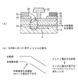
本実施形態による高周波増幅器は、ディジタル・プレディストーション回路401と、ミキサー402a,402bと、パワーアンプ403とを備えて構成される。
ディジタル・プレディストーション回路401は、入力信号の非線形歪みを補償するものである。ミキサー402aは、非線形歪みが補償された入力信号と交流信号をミキシングするものである。パワーアンプ403は、交流信号とミキシングされた入力信号を増幅するものであり、第1、第2の実施形態、及びこれらの諸変形例から選ばれた1種のHEMTを有している。なお図42では、例えばスイッチの切り替えにより、出力側の信号をミキサー402bで交流信号とミキシングしてディジタル・プレディストーション回路401に送出できる構成とされている。
The high frequency amplifier according to the present embodiment includes a
The
本実施形態では、ソース抵抗を低減し、動作速度を向上させることができるHEMTを、高周波増幅器に適用する。これにより、高速動作を可能とする信頼性の高い高周波増幅器が実現する。 In this embodiment, the HEMT that can reduce the source resistance and improve the operation speed is applied to the high-frequency amplifier. As a result, a highly reliable high-frequency amplifier capable of high-speed operation is realized.
以下、化合物半導体装置及びその製造方法、並びに高周波増幅器の諸態様を、付記としてまとめて記載する。 Hereinafter, various aspects of the compound semiconductor device, the manufacturing method thereof, and the high-frequency amplifier will be collectively described as appendices.
(付記1)化合物半導体層と、
前記化合物半導体層の上方に設けられたゲート電極と、
前記化合物半導体層の上方において、前記ゲート電極を挟んで設けられたソース電極及びドレイン電極と
を含み、
前記化合物半導体層は、前記ソース電極と前記ドレイン電極との間の領域のうち、少なくとも前記ソース電極と前記ゲート電極との間に、前記ソース電極に近づくにつれて徐々に深くなる溝が表面に形成されていることを特徴とする化合物半導体装置。
(Appendix 1) a compound semiconductor layer;
A gate electrode provided above the compound semiconductor layer;
A source electrode and a drain electrode provided above the compound semiconductor layer and sandwiching the gate electrode;
The compound semiconductor layer has a surface formed with a groove that gradually becomes deeper toward the source electrode at least between the source electrode and the gate electrode in a region between the source electrode and the drain electrode. A compound semiconductor device.
(付記2)前記化合物半導体層は、前記溝が前記ソース電極と前記ドレイン電極との間に亘って形成されていることを特徴とする付記1に記載の化合物半導体装置。
(Supplementary note 2) The compound semiconductor device according to
(付記3)前記化合物半導体層は、前記溝が、前記ソース電極に近づくにつれて逐次深くなる階段状に形成されていることを特徴とする付記1又は2に記載の化合物半導体装置。
(Supplementary note 3) The compound semiconductor device according to
(付記4)前記化合物半導体層は、少なくとも、電子走行層及び当該電子走行層の上方の電子供給層が積層されており、
前記化合物半導体層は、前記溝が前記電子走行層の途中の深さまで形成されていることを特徴とする付記1〜3のいずれか1項に記載の化合物半導体装置。
(Appendix 4) The compound semiconductor layer includes at least an electron transit layer and an electron supply layer above the electron transit layer,
The compound semiconductor device according to any one of
(付記5)化合物半導体層を形成する工程と、
前記化合物半導体層の上方にソース電極及びドレイン電極を形成する工程と、
前記化合物半導体層の上方において、前記ソース電極と前記ドレイン電極との間に前記ゲート電極を形成する工程と
を含み、
前記化合物半導体層の表面に、前記ソース電極と前記ドレイン電極との間の領域のうち、少なくとも前記ソース電極と前記ゲート電極との間に、前記ソース電極に近づくにつれて徐々に深くなる溝を形成することを特徴とする化合物半導体装置の製造方法。
(Appendix 5) A step of forming a compound semiconductor layer;
Forming a source electrode and a drain electrode above the compound semiconductor layer;
Forming the gate electrode between the source electrode and the drain electrode above the compound semiconductor layer, and
On the surface of the compound semiconductor layer, a groove that gradually becomes deeper as it approaches the source electrode is formed at least between the source electrode and the gate electrode in a region between the source electrode and the drain electrode. A method for manufacturing a compound semiconductor device.
(付記6)前記化合物半導体層の表面に、前記溝を前記ソース電極と前記ドレイン電極との間に亘って形成することを特徴とする付記5に記載の化合物半導体装置の製造方法。 (Additional remark 6) The manufacturing method of the compound semiconductor device of Additional remark 5 characterized by forming the said groove | channel between the said source electrode and the said drain electrode in the surface of the said compound semiconductor layer.
(付記7)前記化合物半導体層の表面に、前記溝を、前記ソース電極に近づくにつれて逐次深くなる階段状に形成することを特徴とする付記5又は6に記載の化合物半導体装置の製造方法。 (Supplementary note 7) The method for manufacturing a compound semiconductor device according to supplementary note 5 or 6, wherein the groove is formed on the surface of the compound semiconductor layer in a stepped shape that gradually becomes deeper as it approaches the source electrode.
(付記8)前記化合物半導体層は、少なくとも、電子走行層及び当該電子走行層の上方の電子供給層が積層されており、
前記化合物半導体層の表面に、前記溝を前記電子走行層の途中の深さまで形成することを特徴とする付記5〜7のいずれか1項に記載の化合物半導体装置の製造方法。
(Supplementary Note 8) The compound semiconductor layer includes at least an electron transit layer and an electron supply layer above the electron transit layer,
8. The method of manufacturing a compound semiconductor device according to any one of appendices 5 to 7, wherein the groove is formed on the surface of the compound semiconductor layer to a depth in the middle of the electron transit layer.
(付記9)入力した高周波電圧を増幅して出力する高周波増幅器であって、
トランジスタを有しており、
前記トランジスタは、
化合物半導体層と、
前記化合物半導体層の上方に設けられたゲート電極と、
前記化合物半導体層の上方において、前記ゲート電極を挟んで設けられたソース電極及びドレイン電極と
を含み、
前記化合物半導体層は、前記ソース電極と前記ドレイン電極との間の領域のうち、少なくとも前記ソース電極と前記ゲート電極との間に、前記ソース電極に近づくにつれて徐々に深くなる溝が表面に形成されていることを特徴とする高周波増幅器。
(Appendix 9) A high frequency amplifier that amplifies and outputs an input high frequency voltage,
Has a transistor,
The transistor is
A compound semiconductor layer;
A gate electrode provided above the compound semiconductor layer;
A source electrode and a drain electrode provided above the compound semiconductor layer and sandwiching the gate electrode;
The compound semiconductor layer has a surface formed with a groove that gradually becomes deeper toward the source electrode at least between the source electrode and the gate electrode in a region between the source electrode and the drain electrode. A high frequency amplifier.
1 化合物半導体積層構造
11 バッファ層
12 ボトムバリア層
13 チャネル層
14 スペーサ層
15 Si−δ−ドーピング層
16 バリア層16
17 i−InP層
18 及びキャップ層
20,40 階段状溝
30,50 テーパ状溝
31 ソース電極
32 ドレイン電極
33 ゲート電極
DESCRIPTION OF
17 i-
Claims (8)
前記化合物半導体層の上方に設けられたゲート電極と、
前記化合物半導体層の上方において、前記ゲート電極を挟んで設けられたソース電極及びドレイン電極と
を含み、
前記化合物半導体層は、前記ソース電極と前記ドレイン電極との間の領域のうち、少なくとも前記ソース電極と前記ゲート電極との間に、前記ソース電極に近づくにつれて徐々に深くなる溝が表面に形成されていることを特徴とする化合物半導体装置。 A compound semiconductor layer;
A gate electrode provided above the compound semiconductor layer;
A source electrode and a drain electrode provided above the compound semiconductor layer and sandwiching the gate electrode;
The compound semiconductor layer has a surface formed with a groove that gradually becomes deeper toward the source electrode at least between the source electrode and the gate electrode in a region between the source electrode and the drain electrode. A compound semiconductor device.
前記化合物半導体層は、前記溝が前記電子走行層の途中の深さまで形成されていることを特徴とする請求項1〜3のいずれか1項に記載の化合物半導体装置。 The compound semiconductor layer includes at least an electron transit layer and an electron supply layer above the electron transit layer,
The compound semiconductor device according to claim 1, wherein in the compound semiconductor layer, the groove is formed to a depth in the middle of the electron transit layer.
前記化合物半導体層の上方にソース電極及びドレイン電極を形成する工程と、
前記化合物半導体層の上方において、前記ソース電極と前記ドレイン電極との間に前記ゲート電極を形成する工程と
を含み、
前記化合物半導体層の表面に、前記ソース電極と前記ドレイン電極との間の領域のうち、少なくとも前記ソース電極と前記ゲート電極との間に、前記ソース電極に近づくにつれて徐々に深くなる溝を形成することを特徴とする化合物半導体装置の製造方法。 Forming a compound semiconductor layer;
Forming a source electrode and a drain electrode above the compound semiconductor layer;
Forming the gate electrode between the source electrode and the drain electrode above the compound semiconductor layer, and
On the surface of the compound semiconductor layer, a groove that gradually becomes deeper as it approaches the source electrode is formed at least between the source electrode and the gate electrode in a region between the source electrode and the drain electrode. A method for manufacturing a compound semiconductor device.
前記化合物半導体層の表面に、前記溝を前記電子走行層の途中の深さまで形成することを特徴とする請求項5〜7のいずれか1項に記載の化合物半導体装置の製造方法。 The compound semiconductor layer includes at least an electron transit layer and an electron supply layer above the electron transit layer,
8. The method of manufacturing a compound semiconductor device according to claim 5, wherein the groove is formed on the surface of the compound semiconductor layer to a depth in the middle of the electron transit layer. 9.
Priority Applications (2)
| Application Number | Priority Date | Filing Date | Title |
|---|---|---|---|
| JP2016050147A JP2017168530A (en) | 2016-03-14 | 2016-03-14 | Compound semiconductor device and manufacturing method thereof |
| US15/452,999 US10079297B2 (en) | 2016-03-14 | 2017-03-08 | Compound semiconductor device |
Applications Claiming Priority (1)
| Application Number | Priority Date | Filing Date | Title |
|---|---|---|---|
| JP2016050147A JP2017168530A (en) | 2016-03-14 | 2016-03-14 | Compound semiconductor device and manufacturing method thereof |
Publications (1)
| Publication Number | Publication Date |
|---|---|
| JP2017168530A true JP2017168530A (en) | 2017-09-21 |
Family
ID=59787173
Family Applications (1)
| Application Number | Title | Priority Date | Filing Date |
|---|---|---|---|
| JP2016050147A Pending JP2017168530A (en) | 2016-03-14 | 2016-03-14 | Compound semiconductor device and manufacturing method thereof |
Country Status (2)
| Country | Link |
|---|---|
| US (1) | US10079297B2 (en) |
| JP (1) | JP2017168530A (en) |
Families Citing this family (5)
| Publication number | Priority date | Publication date | Assignee | Title |
|---|---|---|---|---|
| US10937873B2 (en) * | 2019-01-03 | 2021-03-02 | Cree, Inc. | High electron mobility transistors having improved drain current drift and/or leakage current performance |
| US11127820B2 (en) * | 2019-09-20 | 2021-09-21 | Microsoft Technology Licensing, Llc | Quantum well field-effect transistor and method for manufacturing the same |
| US12082512B2 (en) | 2019-10-24 | 2024-09-03 | Microsoft Technology Licensing, Llc | Semiconductor-superconductor hybrid device |
| US11658233B2 (en) | 2019-11-19 | 2023-05-23 | Wolfspeed, Inc. | Semiconductors with improved thermal budget and process of making semiconductors with improved thermal budget |
| JP7470008B2 (en) * | 2020-10-19 | 2024-04-17 | 株式会社東芝 | Semiconductor Device |
Family Cites Families (5)
| Publication number | Priority date | Publication date | Assignee | Title |
|---|---|---|---|---|
| JP2006005380A (en) | 2001-09-27 | 2006-01-05 | Murata Mfg Co Ltd | Method of manufacturing heterojunction field effect transistor |
| JP2005252276A (en) | 2005-03-24 | 2005-09-15 | Murata Mfg Co Ltd | Manufacturing method for heterojunction metal-oxide semiconductor field-effect transistor |
| JP5331978B2 (en) | 2007-09-03 | 2013-10-30 | 旭化成エレクトロニクス株式会社 | Method of manufacturing field effect transistor and field effect transistor |
| JP5577681B2 (en) * | 2009-11-30 | 2014-08-27 | 住友電気工業株式会社 | Semiconductor device |
| US9660064B2 (en) * | 2013-12-26 | 2017-05-23 | Intel Corporation | Low sheet resistance GaN channel on Si substrates using InAlN and AlGaN bi-layer capping stack |
-
2016
- 2016-03-14 JP JP2016050147A patent/JP2017168530A/en active Pending
-
2017
- 2017-03-08 US US15/452,999 patent/US10079297B2/en not_active Expired - Fee Related
Also Published As
| Publication number | Publication date |
|---|---|
| US10079297B2 (en) | 2018-09-18 |
| US20170263742A1 (en) | 2017-09-14 |
Similar Documents
| Publication | Publication Date | Title |
|---|---|---|
| US9024357B2 (en) | Method for manufacturing a HEMT transistor and corresponding HEMT transistor | |
| US9419121B1 (en) | Semiconductor device with multiple carrier channels | |
| US10910480B2 (en) | Transistor with multi-metal gate | |
| Corrion et al. | Enhancement-mode AlN/GaN/AlGaN DHFET with 700-mS/mm $ g_ {m} $ and 112-GHz $ f_ {T} $ | |
| US10079297B2 (en) | Compound semiconductor device | |
| CN111213244B (en) | High electron mobility transistor with semiconductor layer having thickness varying along transistor width | |
| US20140361341A1 (en) | CASCODE STRUCTURES FOR GaN HEMTs | |
| US9224668B2 (en) | Semiconductor HEMT device with stoichiometric silicon nitride layer | |
| JP2008078601A (en) | High electron mobility transistor structure using gallium nitride having internal electric field electrode for high power as its base | |
| Saha et al. | Scaled β-Ga2O3 thin channel MOSFET with 5.4 MV/cm average breakdown field and near 50 GHz fMAX | |
| JP6880251B2 (en) | High electron mobility transistor with adjustable threshold voltage | |
| US20220376105A1 (en) | Field effect transistor with selective channel layer doping | |
| Panda et al. | Drain dielectric pocket engineering: its impact on the electrical performance of a hetero-structure tunnel FET | |
| Verma et al. | Design and analysis of AlGaN/GaN based DG MOSHEMT for high-frequency application | |
| Shrestha et al. | Design and simulation of high performance lattice matched double barrier normally off AlInGaN/GaN HEMTs | |
| US9786743B2 (en) | Semiconductor device with electron supply layer | |
| KR20230088915A (en) | Field Effect Transistor with At least Partially Recessed Field Plate | |
| US20220302291A1 (en) | Field effect transistor with multiple stepped field plate | |
| JP2000349096A (en) | Compound field effect transistor and its manufacture | |
| US20140252417A1 (en) | Semiconductor device and electronic apparatus | |
| JP5768340B2 (en) | Compound semiconductor device | |
| JP7228701B2 (en) | Local tunneling enhancement for semiconductor devices | |
| JP6810014B2 (en) | Field effect transistor and its manufacturing method | |
| Lu | Ultrawide Bandgap Nitride Semiconductor Heterojunction Field Effect Transistors | |
| JP2015099850A (en) | Transistor using nitride semiconductor, and method of manufacturing the same |