JP2017143114A - Radiation imaging device and radiation imaging system - Google Patents
Radiation imaging device and radiation imaging system Download PDFInfo
- Publication number
- JP2017143114A JP2017143114A JP2016022218A JP2016022218A JP2017143114A JP 2017143114 A JP2017143114 A JP 2017143114A JP 2016022218 A JP2016022218 A JP 2016022218A JP 2016022218 A JP2016022218 A JP 2016022218A JP 2017143114 A JP2017143114 A JP 2017143114A
- Authority
- JP
- Japan
- Prior art keywords
- photoelectric conversion
- radiation imaging
- imaging apparatus
- conversion unit
- radiation
- Prior art date
- Legal status (The legal status is an assumption and is not a legal conclusion. Google has not performed a legal analysis and makes no representation as to the accuracy of the status listed.)
- Pending
Links
Images


Abstract
Description
本発明は、放射線画像を撮像する放射線撮像装置および放射線撮像システムに関する。 The present invention relates to a radiation imaging apparatus and a radiation imaging system that capture a radiation image.
X線等の放射線による医療画像診断や非破壊検査に用いる放射線撮影装置として、TFT(薄膜トランジスタ)等のスイッチと光電変換素子等の変換素子とを組み合わせた画素が配列されたアレイを有する放射線撮像装置が実用化されている。放射線撮像装置の中には、放射線の照射が開始されたことを検出したり、放射線の照射を終了させるべきタイミングを検出したりするために、画素とは別に、放射線の照射を検出する素子を備えるものがある。 Radiation imaging apparatus having an array in which pixels in which a combination of a switch such as a TFT (thin film transistor) and a conversion element such as a photoelectric conversion element is arranged as a radiographic apparatus used for medical image diagnosis and nondestructive inspection using radiation such as X-rays Has been put to practical use. In the radiation imaging apparatus, in order to detect the start of radiation irradiation or to detect the timing for ending radiation irradiation, an element for detecting radiation irradiation is provided separately from the pixels. There is something to prepare.
特許文献1には、撮像用の複数の第1の変換素子と、放射線の照射を検出するために隣接する第1の変換素子の間に配置された第2の変換素子とを有する放射線撮像装置が記載されている。第2の変換素子は、画素ピッチより狭い幅を持つ細長い形状を有する。特許文献2には、放射線画像撮影用の画素と放射線検出用の画素を走査配線と信号配線との交差部に設けた放射線画像撮像装置が記載されている。
特許文献1に記載された放射線撮像装置では、放射線の照射を検出するための第2の変換素子が画素ピッチより狭い幅しか有しない。したがって、例えば、散乱した放射線を除去するためのグリッド(以下、単に「グリッド」という。)や、被検体の肋骨などのように放射線透過率が低い部分の下に第2の変換素子が位置する場合に放射線の検出の精度が低下しうる。換言すると、グリッド又は放射線透過率が低い部分の下に第2の変換素子が位置するかどうかによって第2の変換素子からの出力に大きな差が生じてしまう。また、特許文献2に記載された放射線画像撮像装置においても、放射線検出用の画素が放射線画像撮像用の画素が抜けた部分に配置されているので、特許文献1の放射線撮像装置と同様の問題が生じうる。
In the radiation imaging apparatus described in
本発明は、上記の課題認識を契機としてなされたものであり、放射線照射の検出に対するグリッドや放射線透過率が低い部分の位置の影響を低減するために有利な技術を提供することを目的とする。 The present invention has been made with the above problem recognition as an opportunity, and it is an object of the present invention to provide an advantageous technique for reducing the influence of the position of a grid or a portion having a low radiation transmittance on the detection of radiation irradiation. .
本発明の1つの側面は、放射線を検出する複数の画素が複数の行および複数の列を構成するように配置された撮像領域を有し、前記複数の画素の各々が第1光電変換部を有する放射線撮像装置であって、前記撮像領域に対する放射線の照射を検出する複数の照射検出部を備え、前記複数の照射検出部の各々は、第2光電変換部を含み、前記第2光電変換部は、複数の前記第1光電変換部の隙間に配置され、前記複数の行に沿った第1方向における最大寸法が前記複数の画素のうち1つの行を構成する画素の前記第1方向における配置ピッチより大きく、かつ、前記複数の列に沿った第2方向における最大寸法が前記複数の画素のうち1つの列を構成する画素の前記第2方向における配置ピッチより大きい。 One aspect of the present invention has an imaging region in which a plurality of pixels that detect radiation includes a plurality of rows and a plurality of columns, and each of the plurality of pixels includes a first photoelectric conversion unit. A radiation imaging apparatus having a plurality of irradiation detection units for detecting radiation irradiation to the imaging region, wherein each of the plurality of irradiation detection units includes a second photoelectric conversion unit, and the second photoelectric conversion unit Is arranged in the gap between the plurality of first photoelectric conversion units, and the maximum dimension in the first direction along the plurality of rows is an arrangement in the first direction of pixels constituting one row of the plurality of pixels. The maximum dimension in the second direction along the plurality of columns is larger than the pitch, and is larger than the arrangement pitch in the second direction of pixels constituting one column among the plurality of pixels.
本発明によれば、放射線照射の検出に対するグリッドや放射線透過率が低い部分の位置の影響を低減するために有利な技術が提供される。 According to the present invention, an advantageous technique is provided to reduce the influence of the position of a grid or a portion having a low radiation transmittance on detection of radiation irradiation.
以下、添付図面を参照しながら本発明のその例示的な実施形態を通して説明する。 Hereinafter, exemplary embodiments of the present invention will be described with reference to the accompanying drawings.
この明細書において、放射線の概念には、放射線崩壊によって放出される粒子(光子を含む)の作るビームであるα線、β線、γ線などの他に、同程度以上のエネルギーを有するビーム、例えばX線や粒子線、宇宙線なども含まれるものとする。 In this specification, the concept of radiation includes, in addition to α-rays, β-rays, γ-rays, and the like, which are beams produced by particles (including photons) emitted by radiation decay, For example, X-rays, particle beams, cosmic rays, and the like are included.
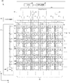
図1には、本発明の第1実施形態の放射線撮像装置DRの構成が示されている。放射線撮像装置DRは、放射線を検出する複数の画素1が複数の行および複数の列を構成するように配置された撮像領域IRを有する。図2には、放射線撮像装置DRの撮像領域IRの一部を拡大した図が示されている。各画素1は、第1光電変換部2を有する。第1光電変換部2は、放射線を直接に電荷に変換するように構成されてもよいし、シンチレータによって放射線から変換された光を電荷に変換するように構成されてもよい。また、各画素1は、第1光電変換部2によって検出された信号を第1読出信号線7に出力する回路として、第1スイッチ2を有しうる。
FIG. 1 shows the configuration of the radiation imaging apparatus DR according to the first embodiment of the present invention. The radiation imaging apparatus DR has an imaging region IR in which a plurality of
放射線撮像装置DRは、露出制御のために、撮像領域IRに対する放射線の照射を検出する複数の照射検出部Sを備えている。露出制御は、例えば、放射線撮像装置DR(撮像領域IR)に対する放射線の照射の開始を検出して、複数の画素1による信号(放射線から変換された電荷)の蓄積を開始することを含みうる。また、露出制御は、放射線撮像装置DR(撮像領域IR)に対する放射線の照射量が規定値に達するタイミングで放射線源による放射線の照射を停止させることを含みうる。
The radiation imaging apparatus DR includes a plurality of irradiation detection units S that detect radiation irradiation on the imaging region IR for exposure control. The exposure control can include, for example, detecting the start of radiation irradiation to the radiation imaging apparatus DR (imaging region IR) and starting accumulation of signals (charges converted from radiation) by the plurality of
各照射検出部Sは、第2光電変換部5を含み、第2光電変換部5は、複数の第1光電変換部2の隙間に配置されている。第2光電変換部5は、放射線を直接に電荷に変換するように構成されてもよいし、シンチレータによって放射線から変換された光を電荷に変換するように構成されてもよい。後者において、シンチレータは、複数の第1光電変換部2および複数の第2光電変換部5において共有されうる。各照射検出部Sは、第2光電変換部5によって検出された信号を第2読出信号線9に出力する回路として、第2スイッチ4を有しうる。
Each irradiation detection unit S includes a second
画素1の第1光電変換部2は、例えば、PIN型センサまたはMIS型センサとして構成されうる。また、照射検出部Sの第2光電変換部5は、例えば、PIN型センサまたはMIS型センサとして構成されうる。
The first
放射線撮像装置DRは、上記の他、制御部31、バイアス電源32、読出部20を備えうる。バイアス電源32は、複数の画素1および複数の照射検出部Sに対してバイアス電圧を供給する。読出部20は、複数の画素1から第1読出信号線7を介して信号を読み出す他、複数の照射検出部Sから第2読出信号線9を介して信号を読み出す。読出部20は、画素1から第1読出信号線7を介して信号を読み出す複数の第1読出回路21、照射検出部Sから第2読出信号線9を介して信号を読み出す複数の第2読出回路22を含む。読出部20は、マルチプレクサ23、ADC(AD変換器)24および信号処理部25を含みうる。マルチプレクサ23は、露出制御時は、複数の読出回路22のからの複数の信号から任意の信号を選択してADC24に出力する。また、マルチプレクサ23は、複数の画素1からの信号を読み出す画像読出時は、複数の読出回路21からの複数の信号を順に選択してADC24に出力する。ADC24は、入力された信号をデジタル信号に変換して信号処理部25に供給する。信号処理部25は、ADC24から供給される信号を処理(例えば、オフセット補正、γ補正など)して出力する。また、信号処理部25は、前述の露出制御のための動作を行うように構成されうる。具体的には、信号処理部25は、放射線撮像装置DR(撮像領域IR)に対する放射線の照射の開始を検出して、複数の画素1による信号(放射線から変換された電荷)の蓄積を開始するように制御部31を制御するように構成されうる。また、信号処理部25は、放射線撮像装置DR(撮像領域IR)に対する放射線の照射量が規定値に達するタイミングで放射線源による放射線の照射を停止させるように構成されうる。
In addition to the above, the radiation imaging apparatus DR may include a
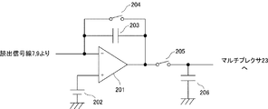
図3に例示されるように、第1読出回路21および第2読出回路22は、例えば、差動増幅器201、基準電圧源202、帰還容量203、短絡スイッチ204、書き込みスイッチ205、保持容量206を含みうる。読出信号線7又は9は、差動増幅器201の反転入力端子に接続され、基準電圧源202は、差動増幅器201の非反転入力端子に接続されうる。差動増幅器201の反転入力端子と出力端子との間には、帰還容量203と短絡スイッチ204とが並列に接続されうる。差動増幅器201の出力端子は、書き込みスイッチ205を介して保持容量206に接続されうる。
As illustrated in FIG. 3, the
再び図1、図2を参照して説明する。複数の画素1の第1光電変換部2の一方の電極(例えば、上部電極)および複数の照射検出部Sの第2光電変換部5の一方の電極(例えば、上部電極)は、共通のバイアス線11に接続されうる。バイアス線11には、バイアス電源32によってバイアス電圧が供給される。
Description will be made with reference to FIGS. 1 and 2 again. One electrode (for example, the upper electrode) of the first
複数の画素1の第1スイッチ3には、制御部31によって駆動される第1制御線6が接続されていて、第1制御信号Vg(Vg1〜Vg6・・・)が供給される。ここで、1つの行を構成する画素1の第1スイッチ3には、1つの第1制御線6が共通に接続されている。複数の照射検出部Sの第2スイッチ4には、制御部31によって駆動される第2制御線8が接続されていて、第2制御信号Vd(Vd1、Vd2・・・)が供給される。ここで、1つの第2制御線8に対して、1つの照射検出部Sの第2スイッチ4が接続されてもよいし、2以上の照射検出部Sの第2スイッチ4が接続されてもよい。第1制御信号Vgおよび第2制御信号Vdは、制御部31によってオン電圧Vonまたはオフ電圧Voffに駆動されうる。オン電圧Vonは、第1スイッチ3、第2スイッチ4をオンさせる電圧であり、オフ電圧Voffは、第1スイッチ3および第2スイッチ4をオフさせる電圧である。
The
ここで、以降における説明のために、行方向および列方向について定義する。行方向は、画素1を制御するための1つの制御線6に接続された画素1が配列された方向である。列方向は、1つの第1読出信号線7に接続された画素1が配列された方向である。
Here, for the following explanation, the row direction and the column direction are defined. The row direction is a direction in which the
撮像領域IRは、複数の関心領域候補(ROI)R1〜R4・・・を有する。関心領域候補のうち露出制御において考慮されうる領域が関心領域である。各関心領域候補は、少なくとも1つの照射検出部Sを含む。図1に示された例では、関心領域候補R1、R2のそれぞれの照射検出部Sが1つの第2読出信号線9に接続され、関心領域候補R3、R4のそれぞれの照射検出部Sが1つの第2読出信号線9に接続されている。また、関心領域候補R1、R3のそれぞれの照射検出部Sの第2スイッチ4は、1つの第2制御線8に接続され、関心領域候補R2、R4のそれぞれの照射検出部Sの第2スイッチ4は、1つの第2制御線8に接続されている。このような構成により、各関心領域候補の照射検出部Sに対するランダムアクセスあるいはXYアドレッシングが可能になり、各関心領域候補の照射検出部Sから信号を読み出すことができる。ここで、第2制御線8および/または第2読出信号線9は、個々の関心領域に対して独立して設けてよい。
The imaging region IR has a plurality of region of interest candidates (ROI) R1 to R4. Of the region of interest candidates, a region that can be considered in exposure control is a region of interest. Each region of interest candidate includes at least one irradiation detection unit S. In the example shown in FIG. 1, each irradiation detection unit S of the region of interest candidates R1 and R2 is connected to one second
図2に例示されるように、第2光電変換部5は、撮像領域IRの複数の行に沿った方向、即ち行方向(第1方向)(図2ではX方向)における最大寸法Sxmaxが、複数の画素1のうち1つの行を構成する画素1の行方向Xにおける配置ピッチPxより大きい。また、第2光電変換部5は、撮像領域IRの複数の列に沿った方向、即ち列方向(第2方向)(図2ではY方向)における最大寸法Symaxが、複数の画素1のうち1つの列を構成する画素1の第2方向Yにおける配置ピッチPyより大きい。なお、図1、2において、画素1を示す点線は、第1光電変換部2が占める領域と等価でありうる。
As illustrated in FIG. 2, the second
このような構成によれば、例えば、グリッドが配置されていて、そのグリッドの配置ピッチが画素1の配置ピッチPx、Pyと略同一である場合でも、照射検出部Sの第2光電変換部5は、グリッドによって放射線が遮断されない領域を有する。これにより、グリッドの影響を低減することができる。図1、2に示された例では、第2光電変換部5は、行方向Xに3画素分、列方向Yに画素分の寸法を有するが、これは例示に過ぎない。
According to such a configuration, for example, even when a grid is arranged and the arrangement pitch of the grid is substantially the same as the arrangement pitch Px, Py of the
上記のような構成は、第2光電変換部5の個数を少なくすること、例えば、画素1の個数より少なくするために有利である。これは、ゲートインジェクションによる影響を低減するために効果的である。第2スイッチ4は、TFT等のトランジスタによって構成されうる。照射検出部Sの第2光電変換部5を読出信号線9に接続するために第2スイッチ4をオンさせるために、第2スイッチ4を構成するトランジスタのゲートに電圧を印加すると、その電圧と容量との積に応じた電荷が第2読出信号線9に転送される。これをゲートインジェクションという。このために第2読出回路22に電荷が流れ込む。第2読出信号線9に接続される複数の照射検出部Sの第2スイッチ4を同時にオンさせると、ゲートインジェクションによる影響が顕著になる。したがって、関心領域候補内に複数の照射検出部Sを配置し、それらから同時に信号を読み出す場合には、ゲートインジェクションの影響を考慮する必要がある。第1実施形態では、複数の画素1(図1、2では、9個の画素1)に対して1つの照射検出部Sが設けられ、また、複数の画素1が配置された領域を横断するように照射検出部Sの第2光電変換部5が配置されている。したがって、1つの第2読出信号線9に対して第2スイッチ4を介して同時に接続される第2光電変換部5の個数が1つであり、これによってゲートインジェクションによる影響が低減される。また、1つの第2制御線8に接続される照射検出部Sの個数を少なくすることにより、第2制御線8の駆動に要する時間(電圧を遷移させるために要する時間)を短くすることができるので、照射検出部Sからの信号の読出周期を短くすることができる。これにより照射検出部Sからの信号の読出の時間分解能を向上させることができる。
Such a configuration is advantageous for reducing the number of second
図4を参照しながら放射線撮像装置RDの動作を説明する。放射線撮像装置RDの動作期間は、第1期間T1、第2期間T2、第3期間T3を含みうる。第1期間T1は、放射線の照射の開始を待つ期間である。第2期間T2は、放射線が照射されている期間である。第3期間T3は、複数の画素1から信号を読み出す期間である。
The operation of the radiation imaging apparatus RD will be described with reference to FIG. The operation period of the radiation imaging apparatus RD may include a first period T1, a second period T2, and a third period T3. The first period T1 is a period of waiting for the start of radiation irradiation. The second period T2 is a period during which radiation is irradiated. The third period T3 is a period for reading signals from the plurality of
第1期間T1は、放射線撮像装置RDの電源がオンされることによって開始する。放射線源(不図示)は、曝射スイッチが操作されることによって放射線の照射を開始する。第1期間T1は、第1制御線6を通して供給される第1制御信号Vg1〜Vgm(Vg1は先頭行、Vgmは最終行を意味する。)を順にオン電圧Vonに駆動することによって各行の画素1の第1光電変換部2の出力電極を第1読出信号線7の電位にリセットする第1動作が行われうる。第1期間T1における第1光電変換部2のリセットは、ダーク電流による電荷が長時間にわたって第1光電変換部2に蓄積されることを防止するためになされうる。
The first period T1 starts when the power of the radiation imaging apparatus RD is turned on. A radiation source (not shown) starts irradiation by operating an exposure switch. In the first period T1, the pixels of each row are driven by sequentially driving the first control signals Vg1 to Vgm (Vg1 means the first row and Vgm means the last row) supplied through the
また、第1期間T1では、第2制御線Vd1〜Vd3・・・を通して供給される第2制御信号Vdを順にオン電圧Vonに駆動することによって複数の照射検出部Sから第2読出信号線9を介して第2読出回路22によって信号を読み出す第2動作が行われうる。図4に示される例では、第1動作および第2動作が交互に行われるが、これらは並行して行われてもよい。信号処理部25は、第2読出回路22によって読み出された信号に基づいて、放射線の照射の開始を検出することができる。即ち、信号処理部25は、撮像領域IRに配置された複数の照射検出部Sの全部または一部の出力に基づいて、放射線の照射の開始を検出しうる。放射線の照射の開始が検出されると、期間T1から期間T2に移行する。
Further, in the first period T1, the second control signal Vd supplied through the second control lines Vd1 to Vd3... Is sequentially driven to the ON voltage Von, whereby the second
あるいは、第2動作は、複数の照射検出部Sの第2光電変換部5の出力電極をリセットする動作で置き換えられてもよい。第1期間T1における第2光電変換部5のリセットは、ダーク電流による電荷が長時間にわたって第2光電変換部5に蓄積されることを防止するためになされうる。複数の第2光電変換部5のリセットは、例えば、第2制御線8を通して供給される第2制御信号Vd1〜Vd3・・・を順にオン電圧Vonに駆動することによって複数の第2光電変換部5の出力電極を第2出信号線9の電位にリセットする動作でありうる。
Alternatively, the second operation may be replaced with an operation of resetting the output electrodes of the second
第1期間T1において、照射検出部Sの第2光電変換部5をリセットする場合には、第2光電変換部5からの信号読出によって放射線の照射の開始を検出することはできない。この場合、信号処理部25は、例えば、曝射スイッチの操作に応答して放射線の照射の開始を知らせる通知を受信することによって、放射線の照射の開始を検出し、第1期間T1の動作を終了し、第2期間の動作に移行しうる。
In the first period T1, when the second
第2期間T2では、第1制御線6を通して駆動される第1制御信号Vg1〜Vgmは、継続してオフ電圧Voffに駆動され、全ての画素1において、第1光電変換部2に電荷が蓄積され続ける。第2期間T2では、信号処理部25は、撮像領域IRの1又は複数の関心領域候補に配置された照射検出部Sから第2読出回路22によって読み出される信号に基づいて放射線の照射を停止させるべきタイミングを決定する。信号処理部25は、放射線の照射を停止させるべきタイミングを決定すると、その決定に応じて、放射線源に放射線の照射を停止させるための指令を送信する。この指令は、放射線源に対して信号処理部25から直接に送信されてもよいし、他の装置を経由して送信されてもよい。
In the second period T2, the first control signals Vg1 to Vgm driven through the
第2期間T2は、放射線の照射量をモニタする期間であるとも言える。第2期間T2では、第2制御線8を介して供給される第2制御信号Vd1〜Vd3・・・が断続的にオン電圧Vonに維持される。これによって、第2スイッチ4がオンした照射検出部Sの第2光電変換部5の信号が第2読出信号線9を介して第2読出回路22によって読み出される。信号処理部25は、撮像領域IRの各関心領域に配置された照射検出部Sから第2読出回路22によって読み出される信号を積算し、積算値に基づいて放射線の照射を停止させるべきタイミングを決定しうる。即ち、信号処理部25は、撮像領域IRに配置された複数の照射検出部Sの全部または一部の出力に基づいて、放射線の照射を停止させるべきタイミングを決定しうる。
It can be said that the second period T2 is a period during which the radiation dose is monitored. In the second period T2, the second control signals Vd1 to Vd3... Supplied via the
第3期間T3では、第1制御線6を介して供給される第1制御信号Vg1〜Vgmを順にオン電圧Vonに駆動することによって各行の画素1の第1光電変換部2から第1読出信号線7を介して第1読出回路21によって読み出される。これによって、複数の画素1の信号によって構成される放射線画像が得られる。
In the third period T3, the first control signals Vg1 to Vgm supplied via the
図5は、1つの画素1の模式的な平面図であり、図6(a)は、図5のA−A’線の模式的な断面図であり、図6(b)は、図5のB−B’線の模式的な断面図である。画素1は、第1光電変換部2と、第1スイッチ素子3とを含む。第1スイッチ3は、TFTで構成され、第1スイッチ3のゲートには、第1制御線6が接続されている。第1スイッチ3の2つの主電極(ソース、ドレイン)105の一方は、第1読出信号線7に接続され、他方は、コンタクトプラグを介して第1光電変換部2の下部電極(出力電極)108に接続されている。第1光電変換部2の上部電極112は、コンタクトプラグを介してバイアス線11に接続されている。
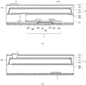
5 is a schematic plan view of one
この例では、第1スイッチ3は、制御電極(ゲート)101、第1絶縁層102、第1半導体層103、第1不純物半導体層104、2つの主電極(ソース、ドレイン)105、第2絶縁層106を有する。第1スイッチ3は、第1層間絶縁層107によって覆われている。第1層間絶縁層107の上には、第1光電変換部2が配置されている。第1光電変換部2は、PIN型光電変換素子として構成されている。第1光電変換部2は、下部電極108の上に、第2不純物半導体層109、第2半導体層110、第3不純物半導体層111、上部電極112、第3絶縁層113を順に有する。第1光電変換部2は、第2層間絶縁層114によって覆われている。第2層間絶縁層114の上には、バイアス線11が配置され、第2層間絶縁層114およびバイアス線11は、第4絶縁層116によって覆われている。
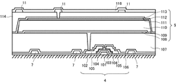
In this example, the
図7は、複数の画素1とそれらの間に配置された照射検出部Sとを示す模式的な平面図である。図8は、図7のC−C’線の模式的な断面図である。前述のように、各照射検出部Sは、1つの第2光電変換部5および1又は複数の第2スイッチ4を含み、第2光電変換部5は、複数の第1光電変換部2の隙間に配置されている。第2スイッチ4もまた複数の第1光電変換部2の隙間に配置されている。第2光電変換部5は、撮像領域IRの行方向(第1方向)(図7ではX方向)における最大寸法Sxmaxが、複数の画素1のうち1つの行を構成する画素1の行方向Xにおける配置ピッチPxより大きい。また、第2光電変換部5は、撮像領域IRの列方向(第2方向)(図7ではY方向)における最大寸法Symaxが、複数の画素1のうち1つの列を構成する画素1の第2方向Yにおける配置ピッチPyより大きい。
FIG. 7 is a schematic plan view showing a plurality of
第2光電変換部5は、第3方向(図7ではX方向)に延びた1又は複数の第1部分51と、第3方向に交差する第4方向(図7ではY方向)に延びた1又は複数の第2部分52とを有しうる。複数の第1光電変換部2の各々は、第3方向に平行な辺および第4方向に平行な辺を有しうる。図7に示された例では、第3方向は、行方向(第1方向)に平行であり、第4方向は、列方向(第2方向)に平行である。
The second
第2光電変換部5は、画素1の配列における複数の行のうちの1つの行である第1行と該第1行に隣接する第2行との間に配置された部分と、該第2行と該第2行に隣接しかつ該第1行とは異なる行である第3行との間に配置された部分とを含みうる。また、第2光電変換部5は、画素1の配列における複数の列のうちの1つの列である第1列と該第1列に隣接する第2列との間に配置された部分と、該第2列と該第2列に隣接しかつ該第1列とは異なる列である第3列との間に配置された部分とを含みうる。あるいは、第2光電変換部5は、#形状部を含みうる。
The second
撮像領域IRが、照射検出部Sが隙間に配置された画素1の第1グループと、照射検出部が隙間に配置されない画素1の第2グループとを含んでもよい。この場合において、第1グループの画素1の第1光電変換部2は、第2グループの画素1の第1光電変換部2よりも面積が小さくてもよいし、同一の面積を有してもよい。前者においては、信号処理部25において、面積の違いに応じて補正がなされうる。後者においては、第2グループの画素1の隙間に、他の検出部が配置されてもよい。例えば、他の検出部は、放射線の照射の開始の検出に利用され、照射検出部Sは、放射線の照射を停止させるタイミングの決定に利用されうる。
The imaging region IR may include a first group of
この例では、第2スイッチ4は、TFTで構成され、第2スイッチ4の制御電極(ゲート)101には、第2制御線8が接続されている。第2スイッチ4の2つの主電極(ソース、ドレイン)105の一方は、第2読出信号線9に接続され、他方は、コンタクトプラグを介して第2光電変換部5の下部電極(出力電極)108に接続されている。第2光電変換部5の上部電極112は、コンタクトプラグを介してバイアス線11に接続されている。
In this example, the
この例では、第2スイッチ4は、制御電極(ゲート)101、第1絶縁層102、第1半導体層103、第1不純物半導体層104、2つの主電極(ソース、ドレイン)105、第2絶縁層106を有する。第1スイッチ3は、第1層間絶縁層107によって覆われている。第1層間絶縁層107の上には、第1光電変換部2が配置されている。第1光電変換部2は、PIN型光電変換素子として構成されている。第2光電変換部5は、下部電極108の上に、第2不純物半導体層109、第2半導体層110、第3不純物半導体層111、上部電極112、第3絶縁層113を順に有する。第2光電変換部5は、第2層間絶縁層114によって覆われている。第2層間絶縁層114の上には、バイアス線11が配置され、第2層間絶縁層114およびバイアス線11は、第4絶縁層116によって覆われている。
In this example, the
ここで、第1スイッチ3および第2スイッチ4において、制御電極(ゲート)101、第1絶縁層102、第1半導体層103、第1不純物半導体層104、2つの主電極105、第2絶縁層106は、それぞれ、互いに同一の層に配置されうる。また、第1光電変換部2および第2光電変換部5において、下部電極108、第2不純物半導体層109、第2半導体層110、第3不純物半導体層111、上部電極112、第3絶縁層113は、それぞれ、互いに同一の層に配置されうる。
Here, in the
図9には、複数の照射検出部Sの配置例が記載されている。なお、図9において、画素1は、図示が省略されている。図9に示された例では、複数の照射検出部Sは、複数の行および複数の列を構成するように配置されている。ただし、複数の画素1によって形成される行および列と複数の照射検出部Sによって構成される行および列とは一致しない。
FIG. 9 shows an arrangement example of the plurality of irradiation detection units S. In FIG. 9, the
図10は、本発明の第2実施形態の放射線撮像装置RDにおける画素1および照射検出部Sの構成を模式的に示す平面図である。第2実施形態は、以下で言及する事項以外については、第1実施形態と同様の構成を有しうる。第2実施形態では、奇数行の画素1と偶数行の画素1とが、行方向に互いに1/2ピッチ(各行の行方向における配置ピッチの1/2)ずらして配置されている。このような配列は、ハニカム構造として理解しうることもできる。
FIG. 10 is a plan view schematically showing the configuration of the
第2光電変換部5は、第3方向に延びた1又は複数の第1部分53と、第3方向に交差する第4方向に延びた1又は複数の第2部分54とを有しうる。また、第2光電変換部5は、第3方向および第4方向に交差する第5方向に延びた1又は複数の第3部分55を有しうる。複数の第1光電変換部2の各々は、第3方向に平行な辺、第4方向に平行な辺、および、第5方向に平行な辺を有しうる。図10に示された例では、第3方向は、行方向(第1方向)および列方向(第2方向)に平行であり、第4方向は、行方向および列方向に交差する方向であり、第5方向は、行方向および列方向に交差する方向である。しかしながら、これは一例に過ぎず、第3方向は行方向(第1方向)および列方向(第2方向)は交差する方向、および/または、第4方向は行方向および列方向に交差する方向、および/または、第5方向は行方向および列方向に交差する方向でありうる。第2実施形態の第2光電変換部5は、行方向および列方向の交差する方向の延びた部分を有するので、グリッドによる影響を低減するために有利である。
The second
第2実施形態においても、第2光電変換部5は、撮像領域IRの行方向(第1方向)(図10ではX方向)における最大寸法Sxmaxが、複数の画素1のうち1つの行を構成する画素1の行方向Xにおける配置ピッチPxより大きい。また、第2光電変換部5は、撮像領域IRの列方向(第2方向)(図10ではY方向)における最大寸法Symaxが、複数の画素1のうち1つの列を構成する画素1の第2方向Yにおける配置ピッチPyより大きい。
Also in the second embodiment, in the second
図11は、本発明の第3実施形態の放射線撮像装置RDにおける画素1および照射検出部Sの構成を模式的に示す平面図である。第3実施形態は、以下で言及する事項以外については、第1又は第2実施形態と同様の構成を有しうる。第3実施形態においても、奇数行の画素1と偶数行の画素1とが、行方向に互いに1/2ピッチ(各行の行方向における配置ピッチの1/2)ずらして配置されている。
FIG. 11 is a plan view schematically showing the configuration of the
第2光電変換部5は、第3方向に延びた1又は複数の第1部分56と、第3方向に交差する第4方向に延びた1又は複数の第2部分57とを有しうる。複数の第1光電変換部2の各々は、第3方向に平行な辺および第4方向に平行な辺を有しうる。図11に示された例では、第3方向は、行方向(第1方向)および列方向(第2方向)に交差する方向であり、第4方向は、行方向および列方向に交差する方向である。しかしながら、これは一例に過ぎず、第3方向は行方向(第1方向)および列方向(第2方向)は交差する方向、および/または、第4方向は行方向および列方向に交差する方向でありうる。第3実施形態の第2光電変換部5もまた、行方向および列方向の交差する方向の延びた部分を有するので、グリッドによる影響を低減するために有利である。
The second
第3実施形態においても、第2光電変換部5は、撮像領域IRの行方向(第1方向)(図11ではX方向)における最大寸法Sxmaxが、複数の画素1のうち1つの行を構成する画素1の行方向Xにおける配置ピッチPxより大きい。また、第2光電変換部5は、撮像領域IRの列方向(第2方向)(図11ではY方向)における最大寸法Symaxが、複数の画素1のうち1つの列を構成する画素1の第2方向Yにおける配置ピッチPyより大きい。
Also in the third embodiment, in the second
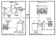
図12には、本発明の一実施形態の放射線撮像システムの構成が記載されている。放射線源であるX線チューブ6050で発生した放射線であるX線6060は、患者あるいは被験者6061の胸部6062を透過し、検出装置6040に含まれる変換素子に入射する。この入射したX線には患者6061の体内部の情報が含まれている。X線の入射に対応して変換部3で放射線を電荷に変換して、電気的情報を得る。この情報はデジタルデータに変換され信号処理手段となるイメージプロセッサ6070により画像処理され制御室の表示手段となるディスプレイ6080で観察できる。
FIG. 12 shows the configuration of a radiation imaging system according to an embodiment of the present invention.
また、この情報は電話回線6090等の伝送処理手段により遠隔地へ転送でき、別の場所のドクタールームなど表示手段となるディスプレイ6081に表示もしくは光ディスク等の記録手段に保存することができ、遠隔地の医師が診断することも可能である。また記録手段となるフィルムプロセッサ6100により記録媒体となるフィルム6110に記録することもできる。
Further, this information can be transferred to a remote place by transmission processing means such as a telephone line 6090, and can be displayed on a display 6081 serving as a display means such as a doctor room in another place or stored in a recording means such as an optical disk. It is also possible for a doctor to make a diagnosis. Moreover, it can also record on the
Claims (16)
前記撮像領域に対する放射線の照射を検出する複数の照射検出部を備え、
前記複数の照射検出部の各々は、第2光電変換部を含み、前記第2光電変換部は、複数の前記第1光電変換部の隙間に配置され、前記複数の行に沿った第1方向における最大寸法が前記複数の画素のうち1つの行を構成する画素の前記第1方向における配置ピッチより大きく、かつ、前記複数の列に沿った第2方向における最大寸法が前記複数の画素のうち1つの列を構成する画素の前記第2方向における配置ピッチより大きい、
ことを特徴とする放射線撮像装置。 A plurality of pixels for detecting radiation have an imaging region arranged to form a plurality of rows and a plurality of columns, and each of the plurality of pixels includes a first photoelectric conversion unit,
A plurality of irradiation detection units for detecting radiation irradiation to the imaging region;
Each of the plurality of irradiation detection units includes a second photoelectric conversion unit, and the second photoelectric conversion unit is disposed in a gap between the plurality of first photoelectric conversion units, and is in a first direction along the plurality of rows. The maximum dimension in the second direction along the plurality of columns is larger than the arrangement pitch in the first direction of pixels constituting one row of the plurality of pixels. Larger than the arrangement pitch of the pixels constituting one column in the second direction,
A radiation imaging apparatus.
ことを特徴とする請求項1に記載の放射線撮像装置。 The second photoelectric conversion unit includes one or more first portions extending in a third direction and one or more second portions extending in a fourth direction intersecting the third direction.
The radiation imaging apparatus according to claim 1.
ことを特徴とする請求項2に記載の放射線撮像装置。 The first photoelectric conversion unit has a side parallel to the third direction and a side parallel to the fourth direction.
The radiation imaging apparatus according to claim 2.
ことを特徴とする請求項3に記載の放射線撮像装置。 The third direction is parallel to the first direction, and the fourth direction is parallel to the second direction.
The radiation imaging apparatus according to claim 3.
ことを特徴とする請求項3に記載の放射線撮像装置。 The third direction is a direction intersecting the first direction and the second direction, and / or the fourth direction is a direction intersecting the first direction and the second direction;
The radiation imaging apparatus according to claim 3.
ことを特徴とする請求項1に記載の放射線撮像装置。 The second photoelectric conversion unit includes one or more first portions extending in a third direction, one or more second portions extending in a fourth direction intersecting the third direction, the third direction, and A third portion extending in a fifth direction intersecting the fourth direction,
The radiation imaging apparatus according to claim 1.
ことを特徴とする請求項6に記載の放射線撮像装置。 The third direction is a direction intersecting the first direction and the second direction, and / or the fourth direction is a direction intersecting the first direction and the second direction, and / or The radiation imaging apparatus according to claim 6, wherein the fifth direction is a direction that intersects the first direction and the second direction.
ことを特徴とする請求項1乃至7のいずれか1項に記載の放射線撮像装置。 The second photoelectric conversion unit includes a portion disposed between a first row that is one of the plurality of rows and a second row adjacent to the first row, the second row, A portion disposed between a third row adjacent to the second row and different from the first row, and a first column and the first column that are one of the plurality of columns And a portion arranged between the second row adjacent to the second row and a third row adjacent to the second row and different from the first row Including,
The radiation imaging apparatus according to claim 1, wherein:
ことを特徴とする請求項1乃至8のいずれか1項に記載の放射線撮像装置。 The second photoelectric conversion unit includes a # shape part,
The radiation imaging apparatus according to claim 1, wherein:
ことを特徴とする請求項1乃至9のいずれか1項に記載の放射線撮像装置。 The second photoelectric conversion unit includes a lower electrode, an upper electrode, and a semiconductor layer disposed between the lower electrode and the upper electrode.
The radiation imaging apparatus according to claim 1, wherein the radiation imaging apparatus is a radiation imaging apparatus.
前記第1光電変換部の前記下部電極と前記第2光電変換部の前記下部電極とは同一の層に配置され、前記第1光電変換部の前記上部電極と前記第2光電変換部の前記上部電極とは同一の層に配置され、前記第1光電変換部の前記半導体層と前記第2光電変換部の前記半導体層とは同一の層に配置されている、
ことを特徴とする請求項10に記載の放射線撮像装置。 The first photoelectric conversion unit includes a lower electrode, an upper electrode, and a semiconductor layer disposed between the lower electrode and the upper electrode,
The lower electrode of the first photoelectric conversion unit and the lower electrode of the second photoelectric conversion unit are arranged in the same layer, and the upper electrode of the first photoelectric conversion unit and the upper part of the second photoelectric conversion unit The electrode is disposed in the same layer, and the semiconductor layer of the first photoelectric conversion unit and the semiconductor layer of the second photoelectric conversion unit are disposed in the same layer,
The radiation imaging apparatus according to claim 10.
前記複数の照射検出部の各々は、前記第2光電変換部を前記読出回路に接続するスイッチを更に含む、
ことを特徴とする請求項1乃至11のいずれか1項に記載の放射線撮像装置。 A read circuit for reading signals from the plurality of irradiation detection units;
Each of the plurality of irradiation detection units further includes a switch that connects the second photoelectric conversion unit to the readout circuit.
The radiation imaging apparatus according to claim 1, wherein the radiation imaging apparatus is a radiation imaging apparatus.
ことを特徴とする請求項1乃至12のいずれか1項に記載の放射線撮像装置。 The number of the plurality of irradiation detection units is less than the number of the plurality of pixels.
The radiation imaging apparatus according to claim 1, wherein the radiation imaging apparatus is a radiation imaging apparatus.
ことを特徴とする請求項1乃至13のいずれか1項に記載の放射線撮像装置。 Based on the output of all or part of the plurality of irradiation detection units, the start of radiation irradiation is detected,
The radiation imaging apparatus according to claim 1, wherein the radiation imaging apparatus is a radiation imaging apparatus.
ことを特徴とする請求項1乃至14のいずれか1項に記載の放射線撮像装置。 Based on the output of all or part of the plurality of irradiation detection units, the timing to stop radiation irradiation is determined,
The radiation imaging apparatus according to claim 1, wherein the radiation imaging apparatus is a radiation imaging apparatus.
前記放射線撮像装置を制御する制御部と、
を備えることを特徴とする放射線撮像システム。 A radiation imaging apparatus according to any one of claims 1 to 15,
A control unit for controlling the radiation imaging apparatus;
A radiation imaging system comprising:
Priority Applications (1)
| Application Number | Priority Date | Filing Date | Title |
|---|---|---|---|
| JP2016022218A JP2017143114A (en) | 2016-02-08 | 2016-02-08 | Radiation imaging device and radiation imaging system |
Applications Claiming Priority (1)
| Application Number | Priority Date | Filing Date | Title |
|---|---|---|---|
| JP2016022218A JP2017143114A (en) | 2016-02-08 | 2016-02-08 | Radiation imaging device and radiation imaging system |
Publications (1)
| Publication Number | Publication Date |
|---|---|
| JP2017143114A true JP2017143114A (en) | 2017-08-17 |
Family
ID=59629167
Family Applications (1)
| Application Number | Title | Priority Date | Filing Date |
|---|---|---|---|
| JP2016022218A Pending JP2017143114A (en) | 2016-02-08 | 2016-02-08 | Radiation imaging device and radiation imaging system |
Country Status (1)
| Country | Link |
|---|---|
| JP (1) | JP2017143114A (en) |
-
2016
- 2016-02-08 JP JP2016022218A patent/JP2017143114A/en active Pending
Similar Documents
| Publication | Publication Date | Title |
|---|---|---|
| JP6570315B2 (en) | Radiation imaging apparatus and radiation imaging system | |
| US11187816B2 (en) | Radiation imaging apparatus and radiation imaging system | |
| JP6378573B2 (en) | Radiation imaging apparatus and radiation imaging system | |
| JP6555909B2 (en) | Radiation imaging apparatus and radiation imaging system | |
| JP5554313B2 (en) | Radiation detector, radiation image capturing apparatus, and radiation image capturing system | |
| US20150316661A1 (en) | Radiation imaging apparatus and radiation imaging system | |
| JP2018191152A (en) | Radiation imaging apparatus, radiation imaging system, control method for radiation imaging apparatus and program | |
| JP2015213221A (en) | Radiation imaging apparatus and radiation imaging system | |
| US11765313B2 (en) | Radiation image capturing apparatus and radiation image capturing system | |
| WO2018135293A1 (en) | Radiation imaging device and radiation imaging system | |
| JP5554258B2 (en) | Radiation detector | |
| JP6470508B2 (en) | Radiation imaging apparatus and radiation imaging system | |
| JP7410678B2 (en) | Radiation imaging devices and radiation imaging systems | |
| JP6512909B2 (en) | Radiation imaging apparatus and radiation imaging system | |
| JP6456127B2 (en) | Radiation imaging apparatus and radiation imaging system | |
| JP7441033B2 (en) | Radiation imaging devices and radiation imaging systems | |
| JP2017143114A (en) | Radiation imaging device and radiation imaging system | |
| JP2018021828A (en) | Radiation imaging apparatus and radiation imaging system | |
| KR102392314B1 (en) | Solid-state imaging device, radiation imaging system, and control method of solid-state imaging device | |
| JP6618251B2 (en) | Radiation imaging apparatus and radiation imaging system | |
| JP6929327B2 (en) | Radiation imaging device and radiation imaging system | |
| JP2004024683A (en) | Apparatus and system for radiation detection | |
| JP6555893B2 (en) | Radiation imaging apparatus and radiation imaging system | |
| JP6436754B2 (en) | Radiation imaging apparatus and radiation imaging system | |
| JP6088628B2 (en) | Radiation detection element, radiation image capturing apparatus, and radiation image capturing system |