JP2017142655A - Electronic information storage medium, information processing method, and information processing program - Google Patents
Electronic information storage medium, information processing method, and information processing program Download PDFInfo
- Publication number
- JP2017142655A JP2017142655A JP2016023546A JP2016023546A JP2017142655A JP 2017142655 A JP2017142655 A JP 2017142655A JP 2016023546 A JP2016023546 A JP 2016023546A JP 2016023546 A JP2016023546 A JP 2016023546A JP 2017142655 A JP2017142655 A JP 2017142655A
- Authority
- JP
- Japan
- Prior art keywords
- initial response
- response data
- update area
- external device
- dummy
- Prior art date
- Legal status (The legal status is an assumption and is not a legal conclusion. Google has not performed a legal analysis and makes no representation as to the accuracy of the status listed.)
- Granted
Links
Images


Abstract
Description
外部機器との間で通信可能なICチップ等の電子情報記憶媒体の技術分野に関する。 The present invention relates to a technical field of an electronic information storage medium such as an IC chip that can communicate with an external device.
従来のICチップは、記憶領域がROM(Read Only Memory)とわずかな不揮発性メモリで構成されていたが、近年、全ての記憶領域が不揮発性メモリで構成されるICチップが増えている。こうしたICチップにおいて不揮発性メモリは、原則的に内容が書き換えられず、プログラム(OS(Operating System)等)を記憶する非更新領域と、頻繁に内容が書き換えられ、プログラムで使用するデータ等を記憶する更新領域とに区別して運用される。 In the conventional IC chip, the storage area is composed of a ROM (Read Only Memory) and a small amount of non-volatile memory. In such an IC chip, in principle, the contents of the nonvolatile memory are not rewritten, the non-update area for storing the program (OS (Operating System), etc.), and the contents are frequently rewritten to store data used in the program. It is operated separately from the update area.
一方で、ICチップは外部機器(例えば、ICチップリーダライタ)から、不揮発性メモリの更新領域に記憶されたデータに対するデータ書き換えコマンドと書き換えデータを受信すると、ICチップのCPUあるいはシーケンサによる書き換え処理手続きを経て、更新領域のデータを書き換える。一般に、更新領域の書き換えには、数ミリ秒の時間が必要である。ICチップのCPUあるいはシーケンサは、書き換え終了までに必要な時間あるいは書き換え終了を示す信号を受信した後、書き換えたデータをベリファイし、書き換え結果の正常/異常を外部機器へ返信する。 On the other hand, when the IC chip receives a data rewrite command and rewrite data for the data stored in the update area of the nonvolatile memory from an external device (for example, an IC chip reader / writer), the rewrite processing procedure by the CPU or sequencer of the IC chip After that, the data in the update area is rewritten. In general, rewriting the update area requires several milliseconds. The CPU or sequencer of the IC chip receives a signal indicating the time required for completion of rewriting or completion of rewriting, verifies the rewritten data, and returns normality / abnormality of the rewriting result to the external device.
また、一般的なICチップには偽造や鍵漏洩を防止するためのプログラムやセンサーが組み込まれているため、使用している最中に発生した物理的な衝撃や信号ノイズによって動作が中断する場合がある。接触式ICチップは、外部機器の電極から電源を供給され、電極を通じて信号を送受信しているため、電極の接点不良や電極に印加されるノイズが動作停止の原因となる。また、非接触式ICチップは外部機器に近づくことにより、磁界をエネルギーとして無結線状態で動作する。このため、非接触式ICチップは、外部機器から離れて、動作に必要なエネルギーの供給を受けなくなると動作が途中で中断する。書き込み処理が停止すると、書き込み途中であったメモリ上のデータの信頼性が損なわれるため、それ以降継続してICチップを使用することが不可能になってしまう。 Also, general IC chips incorporate programs and sensors to prevent counterfeiting and key leakage, so operations are interrupted by physical shocks or signal noise that occur during use There is. The contact IC chip is supplied with power from an electrode of an external device and transmits / receives a signal through the electrode. Therefore, contact failure of the electrode and noise applied to the electrode cause the operation to stop. Further, the non-contact type IC chip operates in a non-connected state using a magnetic field as energy by approaching an external device. For this reason, the operation of the non-contact IC chip is interrupted when it is separated from the external device and is not supplied with the energy necessary for the operation. When the writing process is stopped, the reliability of the data on the memory in the middle of writing is impaired, and it becomes impossible to use the IC chip continuously thereafter.
特許文献1に開示されたICチップでは、書き換え処理を実施する際に、書き換え対象領域のデータを退避させた後に、書き換え処理を実行し、書き換え処理が正常に終了しなかった場合には、動作可能となった時点で、書き換え対象領域を退避データによって書き戻し、退避していたデータを消去するという更新処理を行うことにより、データの信頼性を保持している。
In the IC chip disclosed in
一方で、ICチップ等の通信規格では、ICチップは初期応答要求から規定時間内に初期応答データを返さなければならない旨が定められている。具体的には、ISO/IEC7816(以下、ISO7816という)では初期応答要求から40000外部クロック以内に応答する必要があり、SWP(Single Wire Protocol)では初期応答要求から700μs以内に応答する必要がある。ICチップは、この規定時間内に初期応答データを返信しなければ、外部機器との通信を確立することができない。しかしながら、更新領域に記憶されている初期応答データを返信する場合、更新領域が更新処理中であると規定時間内に返信することができない。特許文献1に開示されたICチップであっても、書き戻しデータが少量であれば、動作可能となった時点において書き戻し処理を実行する方式が有効な場合もあるが、書き戻しデータが一定量を超えると、規定時間を超えてしまうため、ICチップが外部機器との通信を確立することができなくなる。
On the other hand, a communication standard such as an IC chip stipulates that an IC chip must return initial response data within a specified time from an initial response request. Specifically, ISO / IEC7816 (hereinafter referred to as ISO7816) needs to respond within 40000 external clocks from the initial response request, and SWP (Single Wire Protocol) needs to respond within 700 μs from the initial response request. The IC chip cannot establish communication with the external device unless the initial response data is returned within this specified time. However, when the initial response data stored in the update area is returned, it cannot be returned within the specified time if the update area is being updated. Even with the IC chip disclosed in
そこで、本発明は、ICチップ等の電子情報記憶媒体における不揮発性メモリが更新処理中などのためプロセッサが更新領域から初期応答データを読み出すことができない場合に初期応答要求が発生したとしても、外部機器との通信を確立することができる電子情報記憶媒体等を提供することを目的とする。 Therefore, even if an initial response request is generated when the processor cannot read the initial response data from the update area because the nonvolatile memory in the electronic information storage medium such as an IC chip is being updated, the external response An object of the present invention is to provide an electronic information storage medium or the like that can establish communication with a device.
上記課題を解決するために、請求項1に記載の発明は、プロセッサと、前記プロセッサによる更新処理の対象となる更新領域を有する不揮発性メモリとを備え、外部機器との間で通信可能な電子情報記憶媒体であって、前記プロセッサは、前記外部機器から初期応答要求を受信した際に、前記更新領域に記憶された前記外部機器からの初期応答要求に応じて送信する初期応答データを読み出すことができない場合、ダミーの初期応答データを前記外部機器に送信することを特徴とする。
In order to solve the above problem, an invention according to
請求項2に記載の発明は、請求項1に記載の電子情報記憶媒体であって、前記不揮発性メモリは、前記更新処理の対象とならない非更新領域を更に有し、前記ダミーの初期応答データは、前記非更新領域に記憶されており、前記プロセッサは、前記外部機器から初期応答要求を受信した際に、前記更新領域に記憶された前記初期応答データを読み出すことができない場合、前記非更新領域に記憶されている前記ダミーの初期応答データを読み出して、前記外部機器に送信する。 A second aspect of the present invention is the electronic information storage medium according to the first aspect, wherein the nonvolatile memory further includes a non-update area that is not an object of the update process, and the dummy initial response data Is stored in the non-update area, and when the processor cannot read the initial response data stored in the update area when receiving an initial response request from the external device, the non-update The dummy initial response data stored in the area is read and transmitted to the external device.
請求項3に記載の発明は、請求項1に記載の電子情報記憶媒体であって、前記更新処理の対象とならない非更新領域を有するROM(Read Only Memory)を更に備え、前記ダミーの初期応答データは、前記非更新領域に記憶されており、前記プロセッサは、前記外部機器から初期応答要求を受信した際に、前記更新領域に記憶された前記初期応答データを読み出すことができない場合、前記非更新領域に記憶されている前記ダミーの初期応答データを読み出して、前記外部機器に送信することを特徴とする。 A third aspect of the present invention is the electronic information storage medium according to the first aspect, further comprising a ROM (Read Only Memory) having a non-update area that is not an object of the update process, and the dummy initial response Data is stored in the non-update area, and when the processor cannot read the initial response data stored in the update area when receiving an initial response request from the external device, the non-update area The dummy initial response data stored in the update area is read out and transmitted to the external device.
請求項4に記載の発明は、請求項1に記載の電子情報記憶媒体であって、前記プロセッサは、前記外部機器からSWPに応じた初期応答要求を受信した際に、前記更新領域に記憶されたSWPに応じた初期応答データを読み出すことができない場合、乱数を生成することによりSWPに応じた前記ダミーの初期応答データを生成し、当該外部機器に送信することを特徴とする。
The invention according to
請求項5に記載の発明は、プロセッサと、前記プロセッサによる更新処理の対象となる更新領域を有する不揮発性メモリとを備え、外部機器との間で通信可能な電子情報記憶媒体による情報処理方法であって、前記プロセッサが、前記外部機器から初期応答要求を受信した際に、前記更新領域に記憶された前記外部機器からの初期応答要求に応じて送信する初期応答データを読み出すことができない場合、ダミーの初期応答データを前記外部機器に送信する送信工程を含むことを特徴とする。
The invention according to
請求項6に記載の発明は、プロセッサと、前記プロセッサによる更新処理の対象となる更新領域を有する不揮発性メモリとを備え、外部機器との間で通信可能な電子情報記憶媒体における前記プロセッサを、前記外部機器から初期応答要求を受信した際に、前記更新領域に記憶された前記外部機器からの初期応答要求に応じて送信する初期応答データを読み出すことができない場合、ダミーの初期応答データを前記外部機器に送信する送信手段、として機能させることを特徴とする。
The invention according to
本発明によれば、プロセッサが不揮発性メモリの更新領域にアクセスできない場合に初期応答要求が発生したとしても、ダミーの初期応答データを規定時間内に送信することから、外部機器との通信を確立することができる。 According to the present invention, even if an initial response request is generated when the processor cannot access the update area of the nonvolatile memory, the dummy initial response data is transmitted within the specified time, so that communication with the external device is established. can do.
以下、図面を参照して本発明の実施形態について詳細に説明する。以下に説明する実施形態は、通信システムに対して本発明を適用した場合の実施の形態である。 Hereinafter, embodiments of the present invention will be described in detail with reference to the drawings. The embodiment described below is an embodiment when the present invention is applied to a communication system.
まず、図1等を参照して、本実施形態に係る通信システムSの構成及び機能概要を説明する。 First, with reference to FIG. 1 etc., the structure and functional outline | summary of the communication system S which concern on this embodiment are demonstrated.
[1.通信システムSの構成]
図1は、本実施形態に係る通信システムSの概要構成例を示す図である。図1に示すように、通信システムSは、携帯端末1、決済処理端末2、及びホストサーバ3(ホストコンピュータ)等を備えて構成される。ホストサーバ3は、インターネットにより構成される通信ネットワークNWに接続されている。携帯端末1は、無線通信回線(例えば、3G(3rd Generation)回線又はWi−Fi(Wireless Fidelity)回線等)、及び通信ネットワークNWを介してホストサーバ3に接続可能になっており、ホストサーバ3によるサービスの提供を受ける。決済処理端末2は、例えば店舗に設置され、例えばオンライン決済時に専用線を介してホストサーバ3に接続可能になっている。また、決済処理端末2は、当該決済処理端末2に接続された読取器(例えば、ICカードリーダライタ)により発せられる電波により携帯端末1との間で無線通信(例えばNFCの規格で規定される非接触通信)を行いつつ取引の決済処理等を行うことが可能になっている。
[1. Configuration of communication system S]
FIG. 1 is a diagram illustrating a schematic configuration example of a communication system S according to the present embodiment. As shown in FIG. 1, the communication system S includes a
[2.携帯端末1の構成]
図2は、本実施形態に係る携帯端末1の概要構成例を示すブロック図である。図2に示すように、携帯端末1は、制御部11(コンピュータの一例)、記憶部12、無線通信部13、表示部14、入力部15、及びICカードインターフェース16、CLF19等を備えて構成され、これらの構成要素はバス17を介して相互に接続される。なお、携帯端末1は、例えば携帯電話機やスマートフォン等である。
[2. Configuration of mobile terminal 1]
FIG. 2 is a block diagram illustrating a schematic configuration example of the
制御部11は、CPU(Central Processing Unit)、ROM(Read Only Memory)、及びRAM(Random Access Memory)等により構成される。記憶部12は、例えばフラッシュメモリ等の不揮発性メモリにより構成される。上記ROMまたは記憶部12には、オペレーティングシステム(OS)及びミドルウェアが記憶される。また、記憶部12には、携帯端末1にインストールされたAPI(Application Program Interface)及びアプリケーションソフトウェア(アプリケーションプログラム言語から構成されるソフトウェア)等が記憶される。APIは、アプリケーションソフトウェアからオペレーティングシステムの機能を利用するためのインターフェースである。アプリケーションソフトウェアは、例えば所定のサーバからダウンロード可能なプログラムである。
The
無線通信部13は、アンテナを有し、移動体通信網における基地局との間で行われる無線通信を制御する。表示部14は、例えばタッチパネル方式の表示パネルを有し、表示パネルへの表示制御、及びユーザからの操作指示の受け付けを行う。入力部15は、ユーザからの操作指示を入力するための操作ボタンを有し、操作ボタンに応じた信号を制御部11に出力する。ICカードインターフェース16は、制御部11とSIMカード18との間のインターフェース、及び制御部11とCLF19にとの間のインターフェースを担う。
The
SIMカード18は、UICC(Universal Integrated Circuit Card)の一つであり、例えば、従来のSIM(Subscriber Identity Module)をベースに機能を拡張された接触型ICチップを搭載する。CLF19は、外部の決済処理端末2に接続された読取器と電波により通信(例えばNFCの規格で規定される非接触通信)するための非接触型ICチップ(例えばNFCモジュール)である。CLF19には、非接触通信のフィールド内で当該通信を行うためのアンテナが接続されている。なお、CLF19は、携帯端末1のOSにより操作可能になっている。
The
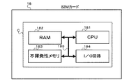
[3.ICチップCの構成]
図3は、本実施形態に係るSIMカード18に搭載されるICチップCの概要構成例を示すブロック図である。図3に示すように、ICチップCは、CPU181(「プロセッサ」の一例)、RAM182、不揮発性メモリ183、及びI/O回路184等を備え、これらの構成要素はバス185を介して相互に接続される。
[3. Configuration of IC chip C]
FIG. 3 is a block diagram illustrating a schematic configuration example of the IC chip C mounted on the
不揮発性メモリ183は、例えばフラッシュメモリであるが、EEPROMであってもよい。不揮発性メモリ183は、図4に示す記憶領域200を有する。記憶領域200は、CPU181による更新処理の対象となる更新領域210と、更新処理の対象とならない非更新領域220から構成される。非更新領域220は、不揮発性メモリ183上のCPU181により更新可能な領域であるが、SIMカード18のライフサイクルにおいて更新されることが想定されない領域である。すなわち、不揮発性メモリ183の記憶領域200には、更新が想定される領域(市場で書き換えが行われる領域)と更新が想定されない領域(市場で書き換えが行われない領域)が存在する。例えば、更新領域210には、OSや各種プログラムが使用するデータ等が記憶される。一方、非更新領域220には、OS、ミドルウェア及び各種プログラム等が記憶される。
The
また、更新領域210には、ISO7816の通信規格に基づきICカードインターフェース16(「外部機器」の一例)から初期応答要求(例えば、C2リセット信号)を受け付けた場合に返信するデータである初期応答データ(ISO7816用)211と、SWPの通信規格に基づきCLF19(「外部機器」の一例)から初期応答要求を受け付けた場合に返信するデータである初期応答データ(SWP用)212が記憶される。
In addition, in the
なお、更新領域210には、CPU181が初期応答データ211、212を読み出せない場合がある。例えば、CPU181による更新処理中である場合や、データの書き換え中に電源が断たれ、値が定まらない状態(安定処理が必要な状態)である場合などである。CPU181はこのような場合に初期応答要求を受け付けると、初期応答データ211、212を読み出せずに、通信規格で定められた規定時間内に初期応答データ211、212を返信することができない。すなわち、通信を確立することができない。
In the
そこで、CPU181が初期応答データ211、212を読み出せない場合であっても、初期応答データを規定時間内に返信することができるように、本実施形態では、非更新領域220にダミーの初期応答データを記憶させる。具体的には、非更新領域220は、初期応答データ(ISO7816用)211のダミーであるダミー初期応答データ(ISO7816用)221と、初期応答データ(SWP用)212のダミーであるダミー初期応答データ(SWP用)222を記憶する。なお、ダミー初期応答データ(ISO7816用)221の値は、初期応答データ(ISO7816用)211と同じ値である。一方、ダミー初期応答データ(SWP用)222については、SWPの通信規格上、初期応答データは固定値ではなく、セッション毎に乱数データを出力することになっている(セッション中は同じ乱数データを使用する)ため、任意の乱数を示す値が記憶される。
Therefore, even if the
I/O回路184は、ISO7816等によって定められた、C1〜C8の8個の接続端子を有する。ここで、C1端子は電源端子(VCC)であり、C5端子はグランド端子(GND)である。また、C2端子は、リセット端子(RST)であり、C3端子は、クロック端子(CLK)である。また、C7端子は、CPU181と制御部11との間の通信のために用いられる。また、C6端子は、CPU181とCLF19との間の通信のために用いられる。なお、上述したように、CPU181とCLF19間の通信プロトコルには、SWP(Single Wire Protocol)が適用される。
The I /
そして、CPU181は、CLF19からのコマンドを受信すると、当該コマンドに応じたコマンド処理を実行し、当該処理の結果を示す応答をCLF19へ行う(返信する)。また、CPU181は、制御部11からのコマンドを受信すると、当該コマンドに応じたコマンド処理を実行し、当該処理の結果を示す応答を制御部11へ行う。
When the
[3.ICチップCの動作]
次に、図5を参照して、CPU181が初期応答要求を受け付けた場合の動作例を説明する。図5は、当該動作例を示すフローチャートである。
[3. Operation of IC chip C]
Next, with reference to FIG. 5, an operation example when the
まず、CPU181は、ICカードインターフェース16からISO7816の通信規格に基づく初期応答要求を受け付けたか否かを判定する(ステップS1)。CPU181は、ISO7816の通信規格に基づく初期応答要求を受け付けていないと判定した場合には(ステップS1:NO)、ステップS6の処理に移行する。一方、CPU181は、ISO7816の通信規格に基づく初期応答要求を受け付けたと判定した場合には(ステップS1:YES)、次いで、更新領域210の初期応答データ(ISO7816用)211を読み出し可能か否かを判定する(ステップS2)。このとき、CPU181は、初期応答データ(ISO7816用)211を読み出し可能であると判定した場合には(ステップS2:YES)、更新領域210の初期応答データ(ISO7816用)211を読み出し、ICカードインターフェース16に送信して(ステップS3)、ステップS6の処理に移行する。一方、CPU181は、初期応答データ(ISO7816用)211を読み出し可能でないと判定した場合には(ステップS2:NO)、非更新領域220に記憶されているダミー初期応答データ(ISO7816用)221を読み出し、ICカードインターフェース16に送信する(ステップS4)。次いで、CPU181は、更新領域210をアクセス可能化処理し(ステップS5)、ステップS6の処理に移行する。アクセス可能化処理とは、CPU181が更新領域にアクセス(読み出し、書き込み)することができるようにする処理である。
First, the
次に、CPU181は、CLF19からSWPの通信規格に基づく初期応答要求を受け付けたか否かを判定する(ステップS6)。CPU181は、SWPの通信規格に基づく初期応答要求を受け付けていないと判定した場合には(ステップS6:NO)、ステップS1の処理に移行する。一方、CPU181は、SWPの通信規格に基づく初期応答要求を受け付けたと判定した場合には(ステップS6:YES)、次いで、更新領域210の初期応答データ(SWP用)212を読み出し可能か否かを判定する(ステップS7)。このとき、CPU181は、初期応答データ(SWP用)212を読み出し可能であると判定した場合には(ステップS7:YES)、更新領域210の初期応答データ(SWP用)212を読み出し、CLF19に送信して(ステップS8)、ステップS1の処理に移行する。一方、CPU181は、初期応答データ(SWP用)212を読み出し可能でないと判定した場合には(ステップS7:NO)、非更新領域220に記憶されているダミー初期応答データ(SWP用)222を読み出し、CLF19に送信する(ステップS9)。次いで、CPU181は、更新領域210をアクセス可能化処理する(ステップS10)。次いで、CPU181は、ダミー初期応答データ(SWP用)222で、更新領域210の初期応答データ(SWP用)212を上書きし(ステップS11)、ステップS1の処理に移行する。これにより、ダミー初期応答データ(SWP用)222と、初期応答データ(SWP用)212は同じ値となる。
Next, the
以上説明したように、本実施形態におけるICチップC(「電子情報記憶媒体」の一例)は、CPU181(「プロセッサ」の一例)と、CPU181による更新処理の対象となる更新領域210と更新処理の対象とならない非更新領域220を有する不揮発性メモリ183とを備え、ICカードインターフェース16(「外部機器」の一例)やCLF19(「外部機器」の一例)との間で通信可能であり、CPU181は、ICカードインターフェース16やCLF19から初期応答要求を受信した際に、更新領域210に記憶された初期応答要求に応じて送信する初期応答データ211、212を読み出すことができない場合、ダミーの初期応答データ221、222をICカードインターフェース16やCLF19に送信する。
As described above, the IC chip C (an example of “electronic information storage medium”) in the present embodiment includes the CPU 181 (an example of “processor”), the
また、ダミーの初期応答データ221、222は、非更新領域220に記憶されており、CPU181は、ICカードインターフェース16やCLF19から初期応答要求を受信した際に、更新領域210に記憶された初期応答データ211、212を読み出すことができない場合、非更新領域220に記憶されているダミーの初期応答データ221、222を読み出して、ICカードインターフェース16やCLF19に送信する。
The dummy
したがって、本実施形態のICチップCによれば、CPU181が不揮発性メモリ183の更新領域210にアクセスできない場合に初期応答要求が発生したとしても、ダミーの初期応答データ221、222を規定時間内に送信することから、ICカードインターフェース16やCLF19との通信を確立することができる。
Therefore, according to the IC chip C of this embodiment, even if the
特にISO7816とSWPに対応するICチップではISO7816とSWPはお互いに独立して初期応答要求が発生する。仮にISO7816の初期応答送信後に更新領域210のメモリ復旧を行う場合でもその間にSWPの初期応答要求が発生する可能性がある。その場合、メモリ復旧の対象エリアに初期応答データ(SWP用)212が格納されていると当該対象エリアにアクセスできずメモリ復旧後にアクセスするとSWPの初期応答の返送の規定時間を越えてしまう可能性がある。そのため、メモリ復旧が必要と判断した場合には双方のダミーの初期応答データに切り替えて対応することでメモリ復旧中の初期応答要求にも対応することが可能となる。
In particular, in an IC chip corresponding to ISO 7816 and SWP, ISO 7816 and SWP generate an initial response request independently of each other. Even if the memory of the
[4.変形例]
次に、上記実施形態の変形例について説明する。なお、以下に説明する変形例は適宜組み合わせることができる。
[4. Modified example]
Next, a modification of the above embodiment will be described. Note that the modifications described below can be combined as appropriate.
[4.1.変形例1]
上記実施形態では、非更新領域220にダミー初期応答データ(SWP用)を記憶させることとしたが、非更新領域220にダミー初期応答データ(SWP用)を記憶させずに、CPU181がSWPの通信規格に基づく初期応答要求を受け付けた際、初期応答データ(SWP用)を読み出し可能でないと判定した場合に、乱数を生成して、当該乱数をダミー初期応答データ(SWP用)として送信することとしてもよい。すなわち、CPU181は、図5のステップS9の処理の代わりに、乱数を生成して、当該乱数をダミー初期応答データ(SWP用)として送信する。これにより、非更新領域220にダミー初期応答データ(SWP用)を記憶させなくとも、CPU181が更新領域210にアクセスできない場合にSWPの通信規格に基づく初期応答要求が発生したとしても、ダミー初期応答データ(SWP用)を規定時間内に送信することから、通信を確立することができる。
[4.1. Modification 1]
In the above embodiment, the dummy initial response data (for SWP) is stored in the
[4.2.変形例2]
上記実施形態では、2つの通信規格(ISO7816とSWP)による通信を確立するためにそれぞれについて初期応答データ及びダミー初期応答データを記憶することとしたが、使用する通信規格の数に応じて、初期応答データ及びダミー初期応答データをそれぞれ記憶することができる。
[4.2. Modification 2]
In the above embodiment, the initial response data and the dummy initial response data are stored for each of the two communication standards (ISO7816 and SWP) to establish communication. However, depending on the number of communication standards used, Response data and dummy initial response data can be stored.
例えば、ISO7816の通信規格のみ使用する場合には、更新領域210に初期応答データ(ISO7816用)211を記憶させ、非更新領域220にダミー初期応答データ(ISO7816用)221を記憶させることとし(初期応答データ(SWP用)212及びダミー初期応答データ(SWP用)222を記憶させない)、図5のフローチャートでは、ステップS6の処理に移行する場合(ステップS1で「NO」判定した場合、ステップS3、S5を終了した場合)には、ステップS1の処理に移行することとする。また、ISO7816及びSWPに加えて、3つ目の通信規格を使用する場合には、当該3つめの通信規格に応じた初期応答データを更新領域210に記憶させ、当該3つめの通信規格に応じたダミーの初期応答データを非更新領域220に記憶させることとする。
For example, when only the ISO 7816 communication standard is used, initial response data (for ISO 7816) 211 is stored in the
[4.3.変形例3]
更新領域210の初期応答データ(ISO7816用)211又は初期応答データ(SWP用)212が読み出し不可能な場合(ステップ2:NO、ステップS7:NO)に、それぞれ非更新領域220のダミー初期応答データ(ISO7816用)221又はダミー初期応答データ(SWP用)222を読み出して送信した場合、当該送信したダミー初期応答データをRAM182にコピーしておき、以降、初期応答要求を受け付けた際には、RAM182上のダミー初期応答データを送信することとしてもよい。これにより、例えば、ダミー初期応答データ(ISO7816用)221をRAM182にコピーしておくことにより、SWPに関するコマンドの実行中に書き換えが発生し、初期応答データ(ISO7816用)211が読み出しできない場合に、ISO7816の通信規格に基づく初期応答要求を受け付けたとしても即時にRAM182上のダミー初期応答データ(ISO7816用)221を送信することができる。
[4.3. Modification 3]
When the initial response data (for ISO7816) 211 or the initial response data (for SWP) 212 in the
また、CPU181は、更新領域210へのアクセスが不可能な状態になった場合に、非更新領域220のダミー初期応答データ(ISO7816用)221及びダミー初期応答データ(SWP用)222を、RAM182にコピーすることとし、この状態で初期応答要求を受け付けた際には、当該初期応答要求の通信規格(ISO7816か、SWPか)に対応するRAM182上のダミー初期応答データ(ISO7816用)221又はダミー初期応答データ(SWP用)222を送信することとしてもよい。これにより、更新領域に210にアクセスが不可能な状態であっても、初期応答要求を受け付けた際に即座に初期応答データを送信することができる。
Further, when the access to the
更にまた、CPU181が初期応答要求を受け付けた際に、当該初期応答要求の通信規格(ISO7816か、SWPか)に応じた初期応答データ211、212又はダミー初期応答データ221、222をRAM182にコピーしておくこととし(更新領域210の初期応答データ211、212が読み込み不可能な場合にはダミー初期応答データ221、222をコピーし、一方、更新領域210の初期応答データ211、212が読み込み可能な場合には初期応答データ211、212をコピーする)、同一セッション中に再度初期応答要求を受け付けた場合には、当該初期応答要求の通信規格に応じたRAM182上の初期応答データ211、212又はダミー初期応答データ221、222を送信することとしてもよい。つまり、CPU181は、初期応答要求を受け付けた場合にRAM182上の出力領域に初期応答データ211、212又はダミー初期応答データ221、222をコピーしておいて出力することとする。これは、初期応答データは電源が切れない限り(同一電源セッションの間)、RAM182上にコピーした同じ初期応答データを送信するという考え方に基づく。これにより、同一電源セッションにおいて初期応答要求を受け付けた際に通信規格に応じた同一の初期応答データを送信することができ、外部機器との通信を円滑に行うことができる。
Furthermore, when the
[4.4.変形例4]
上記実施形態では、ダミー初期応答データ(ISO7816用)221とダミー初期応答データ(SWP用)222を非更新領域220に記憶させることとしたが、これに代えて、ICチップC内にROMを更に設けて、当該ROMにダミー初期応答データ(ISO7816用)221とダミー初期応答データ(SWP用)222を記憶させることとしてもよい。そして、CPU181は、ステップS2の処理において、更新領域210の初期応答データ(ISO7816用)211を読み出し可能でないと判定した場合には(ステップS2:NO)、ICチップC内のROMに記憶されているダミー初期応答データ(ISO7816用)221を読み出し、ICカードインターフェース16に送信したり(ステップS4)、また、ステップS7の処理において、更新領域210の初期応答データ(SWP用)212を読み出し可能でないと判定した場合には(ステップS7:NO)、ICチップC内のROMに記憶されているダミー初期応答データ(SWP用)222を読み出し、CLF19に送信したりしてもよい(ステップS9)。
[4.4. Modification 4]
In the above embodiment, the dummy initial response data (for ISO7816) 221 and the dummy initial response data (for SWP) 222 are stored in the
S 通信システム
1 携帯端末
11 制御部
12 記憶部
13 無線通信部
14 表示部
15 入力部
16 ICカードインターフェース
17 バス
18 SIMカード
C ICチップ
181 CPU
182 RAM
183 不揮発性メモリ
200 記憶領域
210 更新領域
211 初期応答データ(ISO7816用)
212 初期応答データ(SWP用)
220 非更新領域
221 ダミー初期応答データ(ISO7816用)
222 ダミー初期応答データ(SWP用)
184 I/O回路
2 決済処理端末
3 ホストサーバ
182 RAM
183
212 Initial response data (for SWP)
220
222 Dummy initial response data (for SWP)
184 I /
Claims (6)
前記プロセッサは、前記外部機器から初期応答要求を受信した際に、前記更新領域に記憶された前記外部機器からの初期応答要求に応じて送信する初期応答データを読み出すことができない場合、ダミーの初期応答データを前記外部機器に送信することを特徴とする電子情報記憶媒体。 An electronic information storage medium comprising a processor and a non-volatile memory having an update area to be updated by the processor, and capable of communicating with an external device,
When the processor cannot read the initial response data transmitted in response to the initial response request from the external device stored in the update area when receiving the initial response request from the external device, Response data is transmitted to the external device.
前記不揮発性メモリは、前記更新処理の対象とならない非更新領域を更に有し、
前記ダミーの初期応答データは、前記非更新領域に記憶されており、
前記プロセッサは、前記外部機器から初期応答要求を受信した際に、前記更新領域に記憶された前記初期応答データを読み出すことができない場合、前記非更新領域に記憶されている前記ダミーの初期応答データを読み出して、前記外部機器に送信することを特徴とする電子情報記憶媒体。 The electronic information storage medium according to claim 1,
The non-volatile memory further has a non-update area that is not subject to the update process,
The dummy initial response data is stored in the non-update area,
When the processor cannot read the initial response data stored in the update area when receiving an initial response request from the external device, the dummy initial response data stored in the non-update area Is read out and transmitted to the external device.
前記更新処理の対象とならない非更新領域を有するROM(Read Only Memory)を更に備え、
前記ダミーの初期応答データは、前記非更新領域に記憶されており、
前記プロセッサは、前記外部機器から初期応答要求を受信した際に、前記更新領域に記憶された前記初期応答データを読み出すことができない場合、前記非更新領域に記憶されている前記ダミーの初期応答データを読み出して、前記外部機器に送信することを特徴とする電子情報記憶媒体。 The electronic information storage medium according to claim 1,
A ROM (Read Only Memory) having a non-update area that is not subject to the update process;
The dummy initial response data is stored in the non-update area,
When the processor cannot read the initial response data stored in the update area when receiving an initial response request from the external device, the dummy initial response data stored in the non-update area Is read out and transmitted to the external device.
前記プロセッサは、前記外部機器からSWPに応じた初期応答要求を受信した際に、前記更新領域に記憶されたSWPに応じた初期応答データを読み出すことができない場合、乱数を生成することによりSWPに応じた前記ダミーの初期応答データを生成し、当該外部機器に送信することを特徴とする電子情報記憶媒体。 The electronic information storage medium according to claim 1,
When the processor cannot read the initial response data corresponding to the SWP stored in the update area when receiving the initial response request corresponding to the SWP from the external device, the processor generates a random number in the SWP. An electronic information storage medium characterized by generating the initial response data of the corresponding dummy and transmitting it to the external device.
前記プロセッサが、前記外部機器から初期応答要求を受信した際に、前記更新領域に記憶された前記外部機器からの初期応答要求に応じて送信する初期応答データを読み出すことができない場合、ダミーの初期応答データを前記外部機器に送信する送信工程を含むことを特徴とする情報処理方法。 An information processing method using an electronic information storage medium comprising a processor and a nonvolatile memory having an update area to be updated by the processor, and capable of communicating with an external device,
When the processor cannot read the initial response data transmitted in response to the initial response request from the external device stored in the update area when receiving the initial response request from the external device, a dummy initial An information processing method comprising a transmission step of transmitting response data to the external device.
前記外部機器から初期応答要求を受信した際に、前記更新領域に記憶された前記外部機器からの初期応答要求に応じて送信する初期応答データを読み出すことができない場合、ダミーの初期応答データを前記外部機器に送信する送信手段、
として機能させることを特徴とする情報処理プログラム。 The processor in an electronic information storage medium comprising a processor and a non-volatile memory having an update area to be updated by the processor, and capable of communicating with an external device.
When initial response data to be transmitted in response to the initial response request from the external device stored in the update area cannot be read when the initial response request is received from the external device, dummy initial response data is A transmission means for transmitting to an external device;
An information processing program that functions as a computer program.
Priority Applications (1)
| Application Number | Priority Date | Filing Date | Title |
|---|---|---|---|
| JP2016023546A JP6828246B2 (en) | 2016-02-10 | 2016-02-10 | Electronic information storage media, information processing methods, and information processing programs |
Applications Claiming Priority (1)
| Application Number | Priority Date | Filing Date | Title |
|---|---|---|---|
| JP2016023546A JP6828246B2 (en) | 2016-02-10 | 2016-02-10 | Electronic information storage media, information processing methods, and information processing programs |
Related Child Applications (1)
| Application Number | Title | Priority Date | Filing Date |
|---|---|---|---|
| JP2020161822A Division JP2020205120A (en) | 2020-09-28 | 2020-09-28 | Electronic information storage medium, information processing method, and information processing program |
Publications (2)
| Publication Number | Publication Date |
|---|---|
| JP2017142655A true JP2017142655A (en) | 2017-08-17 |
| JP6828246B2 JP6828246B2 (en) | 2021-02-10 |
Family
ID=59627931
Family Applications (1)
| Application Number | Title | Priority Date | Filing Date |
|---|---|---|---|
| JP2016023546A Active JP6828246B2 (en) | 2016-02-10 | 2016-02-10 | Electronic information storage media, information processing methods, and information processing programs |
Country Status (1)
| Country | Link |
|---|---|
| JP (1) | JP6828246B2 (en) |
Cited By (1)
| Publication number | Priority date | Publication date | Assignee | Title |
|---|---|---|---|---|
| WO2020214984A1 (en) | 2019-04-18 | 2020-10-22 | Abbott Diabetes Care Inc. | Systems, devices, and methods for handling wireless communications in an analyte monitoring environment |
-
2016
- 2016-02-10 JP JP2016023546A patent/JP6828246B2/en active Active
Cited By (2)
| Publication number | Priority date | Publication date | Assignee | Title |
|---|---|---|---|---|
| WO2020214984A1 (en) | 2019-04-18 | 2020-10-22 | Abbott Diabetes Care Inc. | Systems, devices, and methods for handling wireless communications in an analyte monitoring environment |
| EP3955804A4 (en) * | 2019-04-18 | 2022-11-23 | Abbott Diabetes Care Inc. | Systems, devices, and methods for handling wireless communications in an analyte monitoring environment |
Also Published As
| Publication number | Publication date |
|---|---|
| JP6828246B2 (en) | 2021-02-10 |
Similar Documents
| Publication | Publication Date | Title |
|---|---|---|
| JP4896837B2 (en) | Portable electronic device and method for controlling portable electronic device | |
| US20120067947A1 (en) | Ic card, mobile electronic device and data processing method in ic card | |
| US9021504B2 (en) | Method and device for automatically selecting an application that can be implemented by said device | |
| US9450751B2 (en) | Smart card, electronic device, and portable electronic device | |
| JP6828246B2 (en) | Electronic information storage media, information processing methods, and information processing programs | |
| US20220398565A1 (en) | Type 4 nfc tags as protocol interface | |
| JP5754287B2 (en) | IC chip, processing method in IC chip, UIM, portable terminal, and processing program for IC chip | |
| JP2020205120A (en) | Electronic information storage medium, information processing method, and information processing program | |
| JP2008310596A (en) | Portable electronic equipment and control method for potable electronic equipment | |
| JP2012093857A (en) | Ic chip, memory initialization method for ic chip, processing program for ic chip, and portable terminal | |
| JP2012008888A (en) | Communication system, communication method, and portable electronic equipment | |
| JP5799754B2 (en) | IC chip, processing method in IC chip, IC chip processing program, IC card, and portable terminal | |
| JP6123539B2 (en) | Identifier generating apparatus, identifier generating method, and identifier generating program | |
| JP2015125627A (en) | Ic card and mobile electronic device | |
| JP6819201B2 (en) | Electronic information storage medium, IC card, setting information transmission method, and setting information transmission program | |
| JP6307938B2 (en) | IC chip, command execution method, and IC chip program | |
| WO2021124846A1 (en) | Ic card and control program for ic card | |
| JP2018156387A (en) | IC card, portable electronic device, program, processing device and processing system | |
| JP6686725B2 (en) | Electronic information storage medium, information processing method, and information processing program | |
| JP6260344B2 (en) | Identifier determining apparatus, identifier determining method, and identifier determining program | |
| JP2018022228A (en) | Electronic information storage medium, determination method, and determination program | |
| JP2020187774A (en) | Electronic information storage medium, ic card, setting information transmitting method, and setting information transmitting program | |
| JP2013164686A (en) | Ic card and portable electronic device | |
| JP2012038297A (en) | Ic chip, processing method of ic chip, processing program for ic chip, and portable terminal | |
| JP2019192143A (en) | Mobile terminal device, mobile terminal device control program, and mobile terminal device control method |
Legal Events
| Date | Code | Title | Description |
|---|---|---|---|
| A621 | Written request for application examination |
Free format text: JAPANESE INTERMEDIATE CODE: A621 Effective date: 20181226 |
|
| A977 | Report on retrieval |
Free format text: JAPANESE INTERMEDIATE CODE: A971007 Effective date: 20191021 |
|
| A131 | Notification of reasons for refusal |
Free format text: JAPANESE INTERMEDIATE CODE: A131 Effective date: 20191119 |
|
| A521 | Written amendment |
Free format text: JAPANESE INTERMEDIATE CODE: A523 Effective date: 20200116 |
|
| A02 | Decision of refusal |
Free format text: JAPANESE INTERMEDIATE CODE: A02 Effective date: 20200630 |
|
| A521 | Written amendment |
Free format text: JAPANESE INTERMEDIATE CODE: A523 Effective date: 20200928 |
|
| C60 | Trial request (containing other claim documents, opposition documents) |
Free format text: JAPANESE INTERMEDIATE CODE: C60 Effective date: 20200928 |
|
| A911 | Transfer to examiner for re-examination before appeal (zenchi) |
Free format text: JAPANESE INTERMEDIATE CODE: A911 Effective date: 20201005 |
|
| C21 | Notice of transfer of a case for reconsideration by examiners before appeal proceedings |
Free format text: JAPANESE INTERMEDIATE CODE: C21 Effective date: 20201006 |
|
| TRDD | Decision of grant or rejection written | ||
| A01 | Written decision to grant a patent or to grant a registration (utility model) |
Free format text: JAPANESE INTERMEDIATE CODE: A01 Effective date: 20201222 |
|
| A61 | First payment of annual fees (during grant procedure) |
Free format text: JAPANESE INTERMEDIATE CODE: A61 Effective date: 20210104 |
|
| R150 | Certificate of patent or registration of utility model |
Ref document number: 6828246 Country of ref document: JP Free format text: JAPANESE INTERMEDIATE CODE: R150 |