JP2017139165A - Mirror device - Google Patents

Mirror device Download PDF

Info

Publication number
JP2017139165A
JP2017139165A JP2016020147A JP2016020147A JP2017139165A JP 2017139165 A JP2017139165 A JP 2017139165A JP 2016020147 A JP2016020147 A JP 2016020147A JP 2016020147 A JP2016020147 A JP 2016020147A JP 2017139165 A JP2017139165 A JP 2017139165A
Authority
JP
Japan
Prior art keywords
sensor
mirror
metal layer
electrode
reflective metal
Prior art date
Legal status (The legal status is an assumption and is not a legal conclusion. Google has not performed a legal analysis and makes no representation as to the accuracy of the status listed.)
Pending
Application number
JP2016020147A
Other languages
Japanese (ja)
Inventor
受田 高明
Takaaki Ukeda
高明 受田
坂元 豪介
Gosuke Sakamoto
豪介 坂元
康平 是澤
Kohei Koresawa
康平 是澤
友香 伊佐治
Yuka Isaji
友香 伊佐治
七井 識成
Satoshige Nanai
識成 七井
Current Assignee (The listed assignees may be inaccurate. Google has not performed a legal analysis and makes no representation or warranty as to the accuracy of the list.)
Panasonic Intellectual Property Management Co Ltd
Original Assignee
Panasonic Intellectual Property Management Co Ltd
Priority date (The priority date is an assumption and is not a legal conclusion. Google has not performed a legal analysis and makes no representation as to the accuracy of the date listed.)
Filing date
Publication date
Application filed by Panasonic Intellectual Property Management Co Ltd filed Critical Panasonic Intellectual Property Management Co Ltd
Priority to JP2016020147A priority Critical patent/JP2017139165A/en
Publication of JP2017139165A publication Critical patent/JP2017139165A/en
Pending legal-status Critical Current

Links

Images

Abstract

PROBLEM TO BE SOLVED: To provide a mirror device capable of suppressing reduction in the sensitivity of a capacitive sensor by a reflective metal layer of a mirror and alleviating a malfunction of an electrostatic capacity sensor due to noise emitted from an electronic device.SOLUTION: The mirror device includes: a mirror 10 having a reflective metal layer 11; an electric device (luminaire 20) disposed around the mirror 10; and a sensor unit 30 disposed on the rear side of the mirror 10 and having a capacitance sensor 31 for operating the electric device. The reflective metal layer 11, the electric device, and the sensor unit 30 have a common ground potential.SELECTED DRAWING: Figure 2

Description

本開示は、鏡を有する洗面化粧台等のミラー装置に関する。   The present disclosure relates to a mirror device such as a vanity having a mirror.

鏡を有するミラー装置として、洗面化粧台やユニットバス等の住宅設備又はミラーキャビネット等が知られている。   As a mirror device having a mirror, a housing facility such as a vanity table or a unit bath or a mirror cabinet is known.

従来、この種のミラー装置として、反射金属層を有する鏡と、照明器具や防曇ヒータ等の電気機器と、電気機器を操作するための操作スイッチとを備える洗面化粧台が提案されている(例えば特許文献1)。このようなミラー装置においては、ユーザが操作スイッチに手を近づけることで電気機器のオンオフ等の操作を行うことができる。   Conventionally, as a mirror device of this type, a vanity is provided that includes a mirror having a reflective metal layer, an electric device such as a lighting fixture or an anti-fogging heater, and an operation switch for operating the electric device ( For example, Patent Document 1). In such a mirror device, the user can perform operations such as turning on / off the electrical device by bringing his hand close to the operation switch.

操作スイッチとしては、センサ電極によってユーザの手の接近に伴う静電容量の変化を検出することで手が接近したことを検知する静電容量センサを用いたセンサスイッチが知られている。   As an operation switch, a sensor switch using a capacitance sensor that detects that a hand has approached by detecting a change in capacitance accompanying the approach of the user's hand with a sensor electrode is known.

特開2004−164893号公報JP 2004-164893 A

しかしながら、上記のような従来のミラー装置では、鏡の反射金属層によって静電容量センサの感度が低下する。つまり、鏡の反射金属層の面積は静電容量センサのセンサ電極の面積よりも1桁以上大きく、静電容量センサにおける静電容量の変化量に対して鏡の反射金属層が持つ寄生容量の方がはるかに大きい。このため、静電容量センサの感度が低下する。   However, in the conventional mirror device as described above, the sensitivity of the capacitance sensor is lowered by the reflective metal layer of the mirror. In other words, the area of the reflective metal layer of the mirror is one digit or more larger than the area of the sensor electrode of the capacitance sensor, and the parasitic capacitance of the reflective metal layer of the mirror with respect to the amount of change in the capacitance of the capacitance sensor. Is much bigger. For this reason, the sensitivity of the capacitance sensor decreases.

また、鏡に設けられた電子機器から発するノイズによって静電容量センサが誤動作する場合もある。   In addition, the capacitance sensor may malfunction due to noise generated from an electronic device provided in the mirror.

また、電気機器のオンオフ等の操作を行うためのセンサスイッチとしては、赤外線センサ(人感センサ)を用いるものもあるが、赤外線センサは熱源に反応するので湯や湯気による誤動作の可能性がある。このため、特に洗面化粧台等の水回り設備のセンサスイッチとしては、赤外線センサではなく、静電容量センサが用いられることが多い。   Some sensor switches for turning on / off electrical devices use infrared sensors (human sensors). However, infrared sensors react to heat sources and may malfunction due to hot water or steam. . For this reason, an electrostatic capacity sensor is often used instead of an infrared sensor as a sensor switch for a watering facility such as a vanity.

本開示は、このような課題を解決するためになされたものであり、鏡と電気機器と静電容量センサとを備えるミラー装置であって、鏡の反射金属層によって静電容量センサの感度が低下することを抑制するとともに、電子機器から発するノイズによって静電容量センサが誤動作することを軽減できるミラー装置を提供することを目的とする。   The present disclosure has been made to solve such a problem, and is a mirror device including a mirror, an electric device, and a capacitance sensor, and the sensitivity of the capacitance sensor is improved by the reflective metal layer of the mirror. It is an object of the present invention to provide a mirror device that can suppress a decrease and reduce malfunction of a capacitance sensor due to noise generated from an electronic device.

上記目的を達成するために、本開示に係るミラー装置の一態様は、反射金属層を有する鏡と、前記鏡の周辺に配置された電気機器と、前記鏡の背面側に配置され、前記電気機器を操作するための静電容量センサを有するセンサユニットとを備え、前記反射金属層と前記電気機器と前記センサユニットとは、共通の接地電位を有する。   In order to achieve the above object, one aspect of a mirror device according to the present disclosure includes a mirror having a reflective metal layer, an electrical device disposed around the mirror, and a back side of the mirror, A sensor unit having a capacitance sensor for operating the device, and the reflective metal layer, the electric device, and the sensor unit have a common ground potential.

本開示によれば、鏡の反射金属層によって静電容量センサの感度が低下することを抑制するとともに、電子機器から発するノイズによって静電容量センサが誤動作することを軽減できる。   According to the present disclosure, it is possible to suppress the sensitivity of the capacitance sensor from being lowered by the reflective metal layer of the mirror, and to reduce the malfunction of the capacitance sensor due to noise generated from the electronic device.

実施の形態に係るミラー装置の正面図である。It is a front view of the mirror device concerning an embodiment. 実施の形態に係るミラー装置の要部拡大正面図である。It is a principal part enlarged front view of the mirror apparatus which concerns on embodiment. 図2のIII-III線における実施の形態に係るミラー装置の断面図である。It is sectional drawing of the mirror apparatus which concerns on embodiment in the III-III line | wire of FIG. 実施の形態に係るミラー装置のセンサユニットに用いられる静電容量センサの平面図である。It is a top view of the electrostatic capacitance sensor used for the sensor unit of the mirror apparatus which concerns on embodiment. 図4のV-V線における静電容量センサの断面図である。It is sectional drawing of the electrostatic capacitance sensor in the VV line of FIG. 静電容量センサによってユーザの手の指を検知する方法を説明するための図である。It is a figure for demonstrating the method to detect a user's hand finger | toe by an electrostatic capacitance sensor. 静電容量センサによってユーザの手の指を検知する他の方法を説明するための図である。It is a figure for demonstrating the other method of detecting a user's hand finger | toe with an electrostatic capacitance sensor. 変形例に係るミラー装置の要部拡大正面図である。It is a principal part enlarged front view of the mirror apparatus which concerns on a modification. 変形例に係る静電容量センサの平面図である。It is a top view of the electrostatic capacitance sensor which concerns on a modification. 図9のX-X線における静電容量センサの断面図である。It is sectional drawing of the electrostatic capacitance sensor in the XX line of FIG.

以下、本開示の実施の形態について説明する。なお、以下に説明する実施の形態は、いずれも本開示の好ましい一具体例を示すものである。したがって、以下の実施の形態で示される、数値、形状、材料、構成要素、構成要素の配置位置及び接続形態などは、一例であって本開示を限定する主旨ではない。よって、以下の実施の形態における構成要素のうち、本開示の最上位概念を示す独立請求項に記載されていない構成要素については、任意の構成要素として説明される。   Hereinafter, embodiments of the present disclosure will be described. Note that each of the embodiments described below shows a preferred specific example of the present disclosure. Therefore, numerical values, shapes, materials, components, arrangement positions of components, connection forms, and the like shown in the following embodiments are merely examples, and are not intended to limit the present disclosure. Therefore, among the constituent elements in the following embodiments, constituent elements that are not described in the independent claims indicating the highest concept of the present disclosure are described as arbitrary constituent elements.

各図は、模式図であり、必ずしも厳密に図示されたものではない。したがって、各図において縮尺等は必ずしも一致していない。各図において、実質的に同一の構成に対しては同一の符号を付しており、重複する説明は省略又は簡略化する。   Each figure is a schematic diagram and is not necessarily shown strictly. Accordingly, the scales and the like do not necessarily match in each drawing. In each figure, substantially the same components are denoted by the same reference numerals, and redundant descriptions are omitted or simplified.

(実施の形態)
実施の形態に係るミラー装置1の構成について、図1〜図5を用いて説明する。図1は、実施の形態に係るミラー装置1の正面図である。図2は、同ミラー装置1の要部拡大正面図である。図3は、図2のIII-III線における断面図である。また、図4は、同ミラー装置1のセンサユニット30に用いられる静電容量センサ31の平面図である。図5は、図4のV-V線における同静電容量センサ31の断面図である。
(Embodiment)
The configuration of the mirror device 1 according to the embodiment will be described with reference to FIGS. FIG. 1 is a front view of a mirror device 1 according to an embodiment. FIG. 2 is an enlarged front view of the main part of the mirror device 1. 3 is a cross-sectional view taken along line III-III in FIG. FIG. 4 is a plan view of a capacitance sensor 31 used in the sensor unit 30 of the mirror device 1. FIG. 5 is a cross-sectional view of the capacitance sensor 31 taken along the line VV in FIG.

図1に示すように、ミラー装置1は、例えば洗面化粧台であり、洗面化粧台の前に立つユーザの姿を映すための鏡10と、洗面台40と、キャビネット50とを備える。本実施の形態におけるミラー装置1は、照明付き洗面化粧台であり、さらに、照明器具20と、照明器具20を操作するためのセンサユニット30とを備える。   As shown in FIG. 1, the mirror device 1 is, for example, a vanity, and includes a mirror 10 for reflecting a user standing in front of the vanity, a vanity 40, and a cabinet 50. The mirror device 1 in the present embodiment is a lighted vanity, and further includes a lighting fixture 20 and a sensor unit 30 for operating the lighting fixture 20.

図2及び図3に示すように、鏡10は、反射金属層11と、反射金属層11の前面側に設けられた透明層12とを有する。つまり、反射金属層11は、透明層12の背面側(裏面側)に設けられている。   As shown in FIGS. 2 and 3, the mirror 10 includes a reflective metal layer 11 and a transparent layer 12 provided on the front side of the reflective metal layer 11. That is, the reflective metal layer 11 is provided on the back side (back side) of the transparent layer 12.

反射金属層11の表面は鏡面となっており、ユーザの姿を映すことができる。反射金属層11は、銀やアルミニウム等の金属からなる金属膜である。透明層12は、例えばガラス層であり、反射金属層11を保護するとともに光を全透過させる機能を有する。反射金属層11は、例えば透明層12としてガラス基板を用いて、このガラス基板の表面に銀やアルミニウムを蒸着することで形成することができる。   The surface of the reflective metal layer 11 is a mirror surface and can reflect the user's appearance. The reflective metal layer 11 is a metal film made of a metal such as silver or aluminum. The transparent layer 12 is a glass layer, for example, and has a function of protecting the reflective metal layer 11 and transmitting light completely. The reflective metal layer 11 can be formed, for example, by using a glass substrate as the transparent layer 12 and depositing silver or aluminum on the surface of the glass substrate.

反射金属層11には、第1開口部11a及び第2開口部11bが形成されている。第1開口部11aは、センサユニット30に対向する位置に形成されている。また、第2開口部11bは、照明器具20に対向する位置に形成されている。本実施の形態では、照明器具20が2つ設けられているので、第2開口部11bも2つ形成されている。なお、鏡10を正面視したときの第1開口部11a及び第2開口部11bの形状は、センサユニット30及び照明器具20の外形に応じた形状とすることができ、例えば矩形状である。   The reflective metal layer 11 has a first opening 11a and a second opening 11b. The first opening 11 a is formed at a position facing the sensor unit 30. In addition, the second opening 11 b is formed at a position facing the lighting fixture 20. In the present embodiment, since two lighting fixtures 20 are provided, two second openings 11b are also formed. In addition, the shape of the 1st opening part 11a and the 2nd opening part 11b when the mirror 10 is viewed in front can be made into the shape according to the external shape of the sensor unit 30 and the lighting fixture 20, for example, is a rectangular shape.

照明器具20は、電気機器の一例であり、鏡10の周辺に配置される。本実施の形態において、照明器具20は、鏡10の背面側に配置されている。具体的には、照明器具20は、鏡10の背面(裏面)に取り付けられている。このため、照明器具20の照明光を前面側に取り出すために、照明器具20の前方部分には反射金属層11が形成されていない。具体的には、反射金属層11における照明器具20の前方部分には第2開口部11bが形成されている。これにより、照明器具20は、第2開口部11bから光を照射できる。つまり、照明器具20から出射した照明光は、第2開口部11bを介して透明層12を透過して鏡10から前方に向けて照射される。   The lighting fixture 20 is an example of an electrical device and is disposed around the mirror 10. In the present embodiment, the lighting fixture 20 is arranged on the back side of the mirror 10. Specifically, the lighting fixture 20 is attached to the back surface (back surface) of the mirror 10. For this reason, in order to take out the illumination light of the lighting fixture 20 to the front side, the reflective metal layer 11 is not formed in the front part of the lighting fixture 20. Specifically, a second opening portion 11 b is formed in the reflective metal layer 11 at the front portion of the lighting fixture 20. Thereby, the lighting fixture 20 can irradiate light from the 2nd opening part 11b. That is, the illumination light emitted from the luminaire 20 passes through the transparent layer 12 through the second opening 11b and is irradiated forward from the mirror 10.

図2及び図3に示すように、照明器具20は、発光モジュール21と、発光モジュール21を収納する器具筐体22とを有する。   As illustrated in FIGS. 2 and 3, the lighting fixture 20 includes a light emitting module 21 and a fixture housing 22 that houses the light emitting module 21.

発光モジュール21は、例えばLEDモジュールであり、白色光を出射する複数の発光素子21aと、基板21bとを有する。発光素子21aは、例えば、LEDによって構成されたLED素子である。基板21bは、所定のパターンで形成された金属配線を有するプリント回路基板である。   The light emitting module 21 is, for example, an LED module, and includes a plurality of light emitting elements 21a that emit white light and a substrate 21b. The light emitting element 21a is, for example, an LED element configured by LEDs. The board 21b is a printed circuit board having metal wiring formed in a predetermined pattern.

器具筐体22は、例えば金属製であるが、樹脂製であってもよい。器具筐体22の鏡10側には開口部が設けられており、発光モジュール21から出射する光はこの開口部を介して器具筐体22の外部に放射される。器具筐体22の開口部は透光板で覆われていてもよい。なお、図示しないが、器具筐体22には、発光モジュール21(発光素子21a)を発光させるための電力を生成する電源回路ユニットが収納されていてもよい。電源回路ユニットで生成された電力は、発光モジュール21に供給される。これにより、発光モジュール21が発光する。   The instrument housing 22 is made of, for example, metal, but may be made of resin. An opening is provided on the mirror housing 10 side of the instrument housing 22, and light emitted from the light emitting module 21 is radiated to the outside of the instrument housing 22 through the opening. The opening of the instrument housing 22 may be covered with a translucent plate. In addition, although not shown in figure, the instrument housing | casing 22 may accommodate the power supply circuit unit which produces | generates the electric power for making the light emitting module 21 (light emitting element 21a) light-emit. The electric power generated by the power supply circuit unit is supplied to the light emitting module 21. Thereby, the light emitting module 21 emits light.

また、照明器具20は、照明光の明るさを制御するための調光機能、及び、照明光の発光色を制御するための調色機能を有していてもよい。照明器具20を調光したり調色したりすることで、周辺の明るさを調整したりユーザの肌の色見をよくしたりすることができる。   Moreover, the lighting fixture 20 may have a light control function for controlling the brightness of illumination light and a color control function for controlling the emission color of illumination light. By dimming or toning the lighting fixture 20, it is possible to adjust the brightness of the surroundings or improve the color of the user's skin.

図2及び図3に示すように、センサユニット30は、ユーザが照明器具20を操作する際にユーザの操作を検知する。センサユニット30は、操作スイッチとして機能し、例えば、照明器具20のオンオフを制御したり照明器具20の調光及び調色を制御したりすることができる。   As shown in FIGS. 2 and 3, the sensor unit 30 detects the user's operation when the user operates the lighting fixture 20. The sensor unit 30 functions as an operation switch. For example, the sensor unit 30 can control on / off of the lighting fixture 20 and can control light adjustment and color adjustment of the lighting fixture 20.

センサユニット30は、鏡10の背面側に配置される。本実施の形態では、センサユニット30は、鏡10の背面に取り付けられている。このため、センサユニット30の前方部分には反射金属層11が形成されていない。具体的には、反射金属層11におけるセンサユニット30の前方部分には第1開口部11aが形成されている。   The sensor unit 30 is disposed on the back side of the mirror 10. In the present embodiment, the sensor unit 30 is attached to the back surface of the mirror 10. For this reason, the reflective metal layer 11 is not formed in the front part of the sensor unit 30. Specifically, a first opening 11 a is formed in the front portion of the sensor unit 30 in the reflective metal layer 11.

センサユニット30は、静電容量センサ31と、静電容量センサ31を収納するセンサ筐体32とを有する。センサ筐体32は、例えば金属製であるが、樹脂製であってもよい。静電容量センサ31は、ユーザが照明器具20を操作するための操作スイッチとして機能する。例えば、ユーザが照明器具20に対してオンオフ制御を行ったり調光制御又は長色制御を行ったりする際に、静電容量センサ31はユーザの操作を検知して、照明器具20に対して操作信号を出力する。   The sensor unit 30 includes a capacitance sensor 31 and a sensor housing 32 that houses the capacitance sensor 31. The sensor housing 32 is made of metal, for example, but may be made of resin. The capacitance sensor 31 functions as an operation switch for the user to operate the lighting fixture 20. For example, when the user performs on / off control, dimming control, or long color control on the lighting fixture 20, the capacitance sensor 31 detects the user's operation and operates the lighting fixture 20. Output a signal.

図4及び図5に示すように、静電容量センサ31は、センサ電極31aと、センサ電極31aが形成された基板31bとを有する。静電容量センサ31は、静電容量式の近接センサ(非接触センサ)であり、センサ電極31aによって静電容量の変化を検出することでユーザの手の接近を検知する。   As shown in FIGS. 4 and 5, the capacitance sensor 31 includes a sensor electrode 31a and a substrate 31b on which the sensor electrode 31a is formed. The capacitance sensor 31 is a capacitance-type proximity sensor (non-contact sensor), and detects the approach of the user's hand by detecting a change in capacitance by the sensor electrode 31a.

センサ電極31aは、基板31bの一方の面(前面側の面)に形成されている。また、センサ電極31aは、反射金属層11に形成された第1開口部11aと対向する位置に配置されている。つまり、金属は電界を遮蔽する効果があるため、センサ電極31aの前面側に反射金属層11が存在するとセンサ電極31aがセンサとして機能しなくなるので、センサ電極31aは反射金属層11には覆われていない。ユーザは、第1開口部11aを介してセンサ電極31aを視認することができ、照明器具20のオンオフ制御等を行う際に、センサ電極31aをスイッチとして操作する。   The sensor electrode 31a is formed on one surface (front surface) of the substrate 31b. The sensor electrode 31 a is disposed at a position facing the first opening 11 a formed in the reflective metal layer 11. That is, since the metal has an effect of shielding the electric field, if the reflective metal layer 11 exists on the front side of the sensor electrode 31a, the sensor electrode 31a does not function as a sensor, so the sensor electrode 31a is covered with the reflective metal layer 11. Not. The user can visually recognize the sensor electrode 31a through the first opening portion 11a, and operates the sensor electrode 31a as a switch when performing on / off control of the lighting fixture 20 or the like.

センサ電極31aは、例えば、銅又は銀等の金属材料によって構成されており、基板31bの一方の面に所定のパターンで形成されている。センサ電極31aは、例えば平面視形状が円形のベタ電極であり、本実施の形態では、基板31bの前面側(鏡10側)の面に2つ形成されている。2つのセンサ電極31aは、所定の間隔をあけて形成されている。また、基板31bは、金属配線が形成された配線基板であり、センサ筐体32に収納されている。   The sensor electrode 31a is made of, for example, a metal material such as copper or silver, and is formed in a predetermined pattern on one surface of the substrate 31b. The sensor electrodes 31a are, for example, solid electrodes having a circular shape in plan view, and in the present embodiment, two sensor electrodes 31a are formed on the front side (mirror 10 side) surface of the substrate 31b. The two sensor electrodes 31a are formed at a predetermined interval. The substrate 31 b is a wiring substrate on which metal wiring is formed, and is housed in the sensor housing 32.

静電容量センサ31は、さらに、センサ電極31aの背面側に配置されたグランド電極31cを有する。グランド電極31cは、基板31bに形成されており、基板31bのセンサ電極31aが形成された面よりも背面側に形成されている。グランド電極31cは、接地電位(グランド電位)に設定されている。   The capacitance sensor 31 further includes a ground electrode 31c disposed on the back side of the sensor electrode 31a. The ground electrode 31c is formed on the substrate 31b, and is formed on the back side of the surface of the substrate 31b where the sensor electrode 31a is formed. The ground electrode 31c is set to a ground potential (ground potential).

本実施の形態では、基板31bとして、絶縁層と配線層との積層構造からなる多層基板を用いており、グランド電極31cは、例えばグランド層であり、多層基板の内層の配線層として形成されている。つまり、グランド電極31cは、多層基板である基板31bのセンサ電極31aが形成された面である一方の面と、当該一の面とは反対側の面である他方の面との間に配置されている。グランド電極31cとしては、ベタ膜からなるベタ電極又はメッシュ状のメッシュ電極等を用いることができる。なお、グランド電極31cの形状は、これらに限るものではなく、所定形状にパターン形成されたものを用いることができる。   In the present embodiment, a multilayer substrate having a laminated structure of an insulating layer and a wiring layer is used as the substrate 31b, and the ground electrode 31c is a ground layer, for example, and is formed as an inner wiring layer of the multilayer substrate. Yes. That is, the ground electrode 31c is arranged between one surface, which is the surface on which the sensor electrode 31a of the substrate 31b, which is a multilayer substrate, is formed, and the other surface, which is the surface opposite to the one surface. ing. As the ground electrode 31c, a solid electrode made of a solid film or a mesh-like mesh electrode can be used. Note that the shape of the ground electrode 31c is not limited to these, and a ground electrode having a pattern formed in a predetermined shape can be used.

また、図2及び図3に示すように、グランド電極31cの一部は、鏡10を正面視したときに、反射金属層11とオーバーラップしている。図2において、グランド電極31cと反射金属層11とがオーバーラップしている箇所に斜線のハッチングを施している。図2に示すように、本実施の形態では、第1開口部11aの開口全周において、グランド電極31cは、反射金属層11とオーバーラップしている。具体的には、グランド電極31cは、第1開口部11aの全領域を覆うように、第1開口部11aの開口全周からはみ出す形で形成されている。   2 and 3, a part of the ground electrode 31c overlaps the reflective metal layer 11 when the mirror 10 is viewed from the front. In FIG. 2, hatched hatching is applied to the portion where the ground electrode 31c and the reflective metal layer 11 overlap. As shown in FIG. 2, in the present embodiment, the ground electrode 31 c overlaps with the reflective metal layer 11 in the entire circumference of the opening of the first opening 11 a. Specifically, the ground electrode 31c is formed so as to protrude from the entire periphery of the first opening 11a so as to cover the entire region of the first opening 11a.

なお、基板31bの他方の面には、センサ電極31aを駆動するための複数の回路部品31d及びコネクタ等が実装されている。複数の回路部品31dは、センサ回路を構成し、検知対象がセンサ電極31aに接近したことによる静電容量の変化を検出する。なお、回路部品31dの前方側にはグランド電極31cが形成されているので、回路部品31dから発生するノイズは、グランド電極31cによって遮蔽することができる。つまり、グランド電極31cは、シールド層として機能する。また、基板31bには、特定電位が印加されたバイアス電極(バイアス層)が別途形成されていてもよい。   A plurality of circuit components 31d and connectors for driving the sensor electrode 31a are mounted on the other surface of the substrate 31b. The plurality of circuit components 31d constitute a sensor circuit and detect a change in capacitance due to the detection target approaching the sensor electrode 31a. Since the ground electrode 31c is formed on the front side of the circuit component 31d, noise generated from the circuit component 31d can be shielded by the ground electrode 31c. That is, the ground electrode 31c functions as a shield layer. Further, a bias electrode (bias layer) to which a specific potential is applied may be separately formed on the substrate 31b.

ここで、静電容量センサ31によってユーザの手の指を検知する方法について、図6を用いて説明する。図6は、静電容量センサ31によってユーザの手の指を検知する方法を説明するための図である。   Here, a method of detecting the finger of the user's hand by the capacitance sensor 31 will be described with reference to FIG. FIG. 6 is a diagram for explaining a method of detecting the finger of the user's hand by the electrostatic capacity sensor 31.

図4に示すように、本実施の形態では、静電容量センサ31は2つのセンサ電極31aを有しており、この2つのセンサ電極31aによってユーザの手が近づいたことを検知することができる。   As shown in FIG. 4, in the present embodiment, the capacitance sensor 31 has two sensor electrodes 31a, and the two sensor electrodes 31a can detect that the user's hand is approaching. .

具体的には、図6に示すようにユーザが照明器具20のオンオフ制御や調光制御等を行う場合、ユーザは、2つのセンサ電極31aの一方の電極の上から他方の電極の上に指先を水平方向に移動させればよい。   Specifically, as shown in FIG. 6, when the user performs on / off control, dimming control, or the like of the lighting device 20, the user moves the fingertip from one electrode of the two sensor electrodes 31 a to the other electrode. May be moved in the horizontal direction.

このとき、2つのセンサ電極31aの各々については、センサ電極31aにユーザの指先が近づくと、センサ電極31aと指との間の静電容量(容量値)が増大し、ユーザの指先が遠ざかると、センサ電極31aと指との間の静電容量(容量値)が減少する。   At this time, for each of the two sensor electrodes 31a, when the user's fingertip approaches the sensor electrode 31a, the capacitance (capacitance value) between the sensor electrode 31a and the finger increases, and the user's fingertip moves away. The electrostatic capacitance (capacitance value) between the sensor electrode 31a and the finger decreases.

したがって、静電容量センサ31は、ユーザの指先が2つのセンサ電極31aの一方の電極の上から他方の電極の上に動いたことで変化する静電容量(容量値)を2つのセンサ電極31aで検出することで、ユーザの指の接近を電気的に検知することができる。なお、容量値の変化は、例えば数pFである。   Accordingly, the capacitance sensor 31 has a capacitance (capacitance value) that changes when the user's fingertip moves from one electrode of the two sensor electrodes 31a to the other electrode. By detecting with, it is possible to electrically detect the approach of the user's finger. Note that the change in capacitance value is, for example, several pF.

静電容量センサ31は、ユーザの指先が接近したことを検知すると検知信号を生成し、生成した検知信号を照明器具20に出力する。これにより、ユーザは照明器具20のオンオフ制御等を行うことができる。   The capacitance sensor 31 generates a detection signal when detecting that the user's fingertip is approaching, and outputs the generated detection signal to the lighting fixture 20. Thereby, the user can perform on / off control of the lighting fixture 20 or the like.

また、本実施の形態では、2つのセンサ電極31aを用いてユーザの手が近づいたことを検知したが、図7に示すように、1つのセンサ電極31aによってユーザの手が近づいたことを検知するように構成されていてもよい。この場合、例えばユーザが指先を静電容量センサ31に接近させたり遠ざけたりする動作を行うことで、静電容量センサ31がユーザの指先が接近したことを検知することができる。   Further, in the present embodiment, it is detected that the user's hand is approaching using the two sensor electrodes 31a, but as shown in FIG. 7, it is detected that the user's hand is approaching using one sensor electrode 31a. It may be configured to. In this case, for example, when the user performs an operation of moving the fingertip closer to or away from the capacitance sensor 31, the capacitance sensor 31 can detect that the user's fingertip has approached.

具体的には、ユーザが照明器具20のオンオフ制御等を行う場合、図7に示すように、ユーザは、静電容量センサ31に指先を近づけて速やかに引くことで、静電容量センサ31は、ユーザの指先が接近したことを検知することができる。この場合、静電容量センサ31は、ユーザの指先が1つのセンサ電極31aに接近させたり遠ざけたりするときにおいてセンサ電極31aとユーザの指先との間に生じる静電容量(容量値)の変化を検出して、ユーザの指先が接近したことを検知して検知信号を生成する。これにより、照明器具20のオンオフ制御等を行うことができる。   Specifically, when the user performs on / off control or the like of the lighting fixture 20, as shown in FIG. 7, the user pulls the fingertip close to the capacitance sensor 31 and quickly pulls the capacitance sensor 31. It is possible to detect that the user's fingertip is approaching. In this case, the capacitance sensor 31 changes the capacitance (capacitance value) generated between the sensor electrode 31a and the user's fingertip when the user's fingertip approaches or moves away from the one sensor electrode 31a. It detects and detects that a user's fingertip approached and generates a detection signal. Thereby, on-off control of the lighting fixture 20 etc. can be performed.

なお、図7に示す検知方法の場合、例えば、2つのセンサ電極31aの一方をオンオフ制御の操作スイッチとして用いて、2つのセンサ電極31aの他方を調光制御の操作スイッチとして用いることができる。   In the case of the detection method shown in FIG. 7, for example, one of the two sensor electrodes 31a can be used as an on / off control operation switch, and the other of the two sensor electrodes 31a can be used as a dimming control operation switch.

また、静電容量センサ31は、検知対象(ユーザの手等)が近接した場合に限らず、検知対象が接触した場合にも検知対象を検知することができる。つまり、静電容量センサ31は非接触又は接触によってセンサ感度を得ることができ、センサユニット30は、非接触操作及び接触操作の両方で照明器具20を操作することができる。   Moreover, the electrostatic capacitance sensor 31 can detect a detection target not only when a detection target (a user's hand etc.) approaches but also when a detection target contacts. That is, the capacitance sensor 31 can obtain sensor sensitivity by non-contact or contact, and the sensor unit 30 can operate the lighting fixture 20 by both non-contact operation and contact operation.

このように構成されるミラー装置1では、図2及び図3に示すように、鏡10の反射金属層11と照明器具20とセンサユニット30とが、接地電位のグランド線60に接続されている。これにより、反射金属層11と照明器具20とセンサユニット30とが共通の接地電位を有する。グランド線60は、アース接続されることで接地電位に設定されている。   In the mirror device 1 configured as described above, as shown in FIGS. 2 and 3, the reflective metal layer 11 of the mirror 10, the lighting fixture 20, and the sensor unit 30 are connected to a ground line 60 having a ground potential. . Thereby, the reflective metal layer 11, the lighting fixture 20, and the sensor unit 30 have a common ground potential. The ground line 60 is set to the ground potential by being grounded.

具体的には、照明器具20では、発光モジュール21の基板21b(回路基板)にグランド線60が接続されている。これにより、基板21bが接地されている。このように、照明器具20では、基板21bが接地されることで接地電位を有する構成となっている。   Specifically, in the lighting fixture 20, the ground line 60 is connected to the substrate 21 b (circuit board) of the light emitting module 21. Thereby, the board | substrate 21b is earth | grounded. Thus, in the lighting fixture 20, it has the structure which has a grounding potential by the board | substrate 21b being earth | grounded.

また、センサユニット30では、静電容量センサ31の基板31bのグランド電極31cにグランド線60が接続されている。このように、センサユニット30では、グランド電極31cが接地されることで接地電位を有する構成となっている。   In the sensor unit 30, the ground wire 60 is connected to the ground electrode 31 c of the substrate 31 b of the capacitance sensor 31. Thus, the sensor unit 30 is configured to have a ground potential by grounding the ground electrode 31c.

以上、本実施の形態に係るミラー装置1によれば、反射金属層11を有する鏡10と、鏡10の周辺に配置された照明器具20と、鏡10の背面側に配置され、照明器具20を操作するための静電容量センサ31を有するセンサユニット30とを備え、反射金属層11と照明器具20とセンサユニット30とは、共通の接地電位を有する。つまり、鏡10と照明器具20とセンサユニット30とを共通接地化している。   As described above, according to the mirror device 1 according to the present embodiment, the mirror 10 having the reflective metal layer 11, the lighting fixture 20 disposed around the mirror 10, and the rear side of the mirror 10, the lighting fixture 20 is provided. The reflective metal layer 11, the lighting fixture 20, and the sensor unit 30 have a common ground potential. That is, the mirror 10, the lighting fixture 20, and the sensor unit 30 are grounded in common.

この構成により、静電容量センサ31のセンサ電極31a周辺の部材(鏡10の反射金属層11、回路部品31dが構成するセンサ回路、照明器具20)が接地されるので、静電容量センサ31が電気的に独立する。この結果、静電容量センサ31に対する鏡10の持つ寄生容量の影響が小さくなるので、静電容量センサ31のセンサ感度が低下することを抑制できる。つまり、静電容量センサ31のセンサ感度が高まる。   With this configuration, the members around the sensor electrode 31a of the capacitance sensor 31 (the reflective metal layer 11 of the mirror 10, the sensor circuit formed by the circuit component 31d, and the lighting fixture 20) are grounded. Electrically independent. As a result, since the influence of the parasitic capacitance of the mirror 10 on the capacitance sensor 31 is reduced, it is possible to suppress the sensor sensitivity of the capacitance sensor 31 from being lowered. That is, the sensor sensitivity of the capacitance sensor 31 is increased.

また、照明器具20から発するノイズ及び外来ノイズも遮蔽することができるので、静電容量センサ31が誤動作することも抑制できる。   Moreover, since the noise emitted from the lighting fixture 20 and the external noise can also be shielded, it is possible to suppress the malfunction of the capacitance sensor 31.

このように、本実施の形態に係るミラー装置1によれば、鏡10と照明器具20とセンサユニット30とを共通接地化することで、鏡10の反射金属層11によって静電容量センサ31の感度が低下することを抑制するとともに、電気機器である照明器具20から発するノイズによって静電容量センサ31が誤動作することを軽減できる。   As described above, according to the mirror device 1 according to the present embodiment, the mirror 10, the lighting fixture 20, and the sensor unit 30 are connected to the common ground, so that the capacitance sensor 31 of the capacitance sensor 31 is formed by the reflective metal layer 11 of the mirror 10. While suppressing that a sensitivity falls, it can reduce that the electrostatic capacitance sensor 31 malfunctions by the noise emitted from the lighting fixture 20 which is an electric equipment.

しかも、鏡10と照明器具20とセンサユニット30とを共通接地化することで、鏡10だけではなく照明器具20及びセンサユニット30も接地電位を有することになる。これにより、湿度が高くて鏡10が結露した場合又は鏡10の表面に水滴が付着した場合であってもユーザが感電してしまうことを防止できる。したがって、ユーザは安全にミラー装置1を使用することができる。   In addition, since the mirror 10, the lighting fixture 20, and the sensor unit 30 are connected to a common ground, not only the mirror 10 but also the lighting fixture 20 and the sensor unit 30 have a ground potential. Thereby, it is possible to prevent the user from getting an electric shock even when the humidity is high and the mirror 10 is condensed or when water droplets adhere to the surface of the mirror 10. Therefore, the user can use the mirror device 1 safely.

また、本実施の形態に係るミラー装置1では、反射金属層11と照明器具20とセンサユニット30とは、接地電位のグランド線60に接続されている。   In the mirror device 1 according to the present embodiment, the reflective metal layer 11, the lighting fixture 20, and the sensor unit 30 are connected to a ground line 60 having a ground potential.

このようにグランド線60を用いることで、反射金属層11と照明器具20とセンサユニット30とを容易に共通の接地電位を有するように構成することができる。   Thus, by using the ground wire 60, the reflective metal layer 11, the lighting fixture 20, and the sensor unit 30 can be easily configured to have a common ground potential.

また、本実施の形態において、センサユニット30は、非接触操作及び接触操作の両方で照明器具20を操作することができる。   Moreover, in this Embodiment, the sensor unit 30 can operate the lighting fixture 20 by both non-contact operation and contact operation.

これにより、センサユニット30の操作の自由度が向上するので、ユーザの利便性が向上する。   Thereby, since the freedom degree of operation of the sensor unit 30 improves, a user's convenience improves.

また、本実施の形態において、静電容量センサ31は、センサ電極31aと、センサ電極31aの背面側に配置されたグランド電極31cとを有し、センサ電極31aは、反射金属層11に形成された第1開口部11aと対向する位置に配置されており、グランド電極31cは、接地されている。そして、グランド電極31cの一部は、鏡10を正面視したときに、反射金属層11とオーバーラップしている。   In the present embodiment, the capacitance sensor 31 includes a sensor electrode 31a and a ground electrode 31c disposed on the back side of the sensor electrode 31a. The sensor electrode 31a is formed on the reflective metal layer 11. The first electrode 11c is disposed at a position facing the first opening 11a, and the ground electrode 31c is grounded. A part of the ground electrode 31 c overlaps the reflective metal layer 11 when the mirror 10 is viewed from the front.

これにより、第1開口部11aがグランド電極31cで覆われるので、鏡10の前面又は背面からの外来ノイズを遮蔽することができる。この結果、静電容量センサ31の周辺領域におけるノイズの回り込みが無くなるので、静電容量センサ31の誤動作を一層抑制することができるとともに、静電容量センサ31のセンサ感度を一層高めることができる。 なお、第1開口部11aをグランド電極31cで完全に覆うことによって、鏡10の前面又は背面からの外来ノイズを完全に遮蔽することができる。   Thereby, since the 1st opening part 11a is covered with the ground electrode 31c, the external noise from the front surface or back surface of the mirror 10 can be shielded. As a result, noise wraparound in the peripheral area of the capacitance sensor 31 is eliminated, so that malfunction of the capacitance sensor 31 can be further suppressed and the sensor sensitivity of the capacitance sensor 31 can be further increased. In addition, the external noise from the front surface or the back surface of the mirror 10 can be completely shielded by completely covering the first opening 11a with the ground electrode 31c.

また、本実施の形態において、静電容量センサ31は、基板31bを有し、基板31bの一方の面にはセンサ電極31aが形成され、基板31bの他方の面にはセンサ電極31aを駆動するための回路部品31dが実装されている。そして、グランド電極31cは、基板31bの一方の面と他方の面との間に配置されている。   In the present embodiment, the capacitance sensor 31 has a substrate 31b, the sensor electrode 31a is formed on one surface of the substrate 31b, and the sensor electrode 31a is driven on the other surface of the substrate 31b. A circuit component 31d is mounted. The ground electrode 31c is disposed between one surface and the other surface of the substrate 31b.

これにより、センサ電極31aを電気的に独立にすることができるので、静電容量センサ31のセンサ感度を高めることができる。   Thereby, since the sensor electrode 31a can be electrically independent, the sensor sensitivity of the capacitance sensor 31 can be increased.

また、本実施の形態では、鏡10の背面側に配置された電気機器として、反射金属層11に形成された第2開口部11bから光を照射できる照明器具20を用いている。   Moreover, in this Embodiment, the lighting fixture 20 which can irradiate light from the 2nd opening part 11b formed in the reflective metal layer 11 is used as an electric equipment arrange | positioned at the back side of the mirror 10. FIG.

これにより、ユーザは、鏡10を利用する際に静電容量センサ31(操作スイッチ)を操作することで、照明器具20を利用することができる。   Thus, the user can use the lighting fixture 20 by operating the capacitance sensor 31 (operation switch) when using the mirror 10.

また、図8に示すように、センサユニット30における金属製のセンサ筐体32も接地されていてもよい。   Moreover, as shown in FIG. 8, the sensor housing 32 made of metal in the sensor unit 30 may also be grounded.

このように、センサ筐体32についても共通の接地電位とすることで、外来ノイズが静電容量センサ31に影響を及ぼすことを抑制できる。しかも、静電容量センサ31のセンサ回路(回路部品)自身から発生する電気的ノイズがセンサ筐体32で封止される。これにより、静電容量センサ31の誤動作を抑制することができる。また、静電容量センサ31のセンサー感度が高まる。   As described above, by setting the sensor casing 32 to the common ground potential, it is possible to suppress the external noise from affecting the capacitance sensor 31. In addition, electrical noise generated from the sensor circuit (circuit component) itself of the capacitance sensor 31 is sealed by the sensor housing 32. Thereby, malfunctioning of the capacitance sensor 31 can be suppressed. In addition, the sensor sensitivity of the capacitance sensor 31 is increased.

この場合、図8に示すように、さらに、照明器具20(電気機器)における金属製の器具筐体22も接地されていてもよい。   In this case, as shown in FIG. 8, the metal fixture housing 22 in the lighting fixture 20 (electric device) may also be grounded.

これにより、照明器具20で発生する電気的ノイズが機器筐体22で封止されるので、照明器具20で発生するノイズによって静電容量センサ31が影響を受けることを抑制できる。これにより、静電容量センサ31の誤動作を一層抑制することができるとともに、静電容量センサ31のセンサー感度が一層高まる。また、器具筐体22を接地することで、外来ノイズが照明器具20に影響を及ぼすことも抑制できる。   Thereby, since the electrical noise which generate | occur | produces with the lighting fixture 20 is sealed with the apparatus housing | casing 22, it can suppress that the electrostatic capacitance sensor 31 is influenced by the noise which generate | occur | produces with the lighting fixture 20. FIG. Thereby, the malfunction of the capacitance sensor 31 can be further suppressed, and the sensor sensitivity of the capacitance sensor 31 is further increased. Moreover, it can suppress that external noise influences the lighting fixture 20 by earth | grounding the fixture housing | casing 22. FIG.

(変形例等)
以上、本発明に係るミラー装置について、実施の形態に基づいて説明したが、本発明は、上記実施の形態に限定されるものではない。
(Modifications, etc.)
As described above, the mirror device according to the present invention has been described based on the embodiment, but the present invention is not limited to the above embodiment.

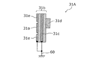
例えば、図9及び図10に示すように、静電容量センサ31Aとして、センサ電極31aの周囲にグランド電極31eが形成されたものを用いてもよい。図9は、変形例に係る静電容量センサ31Aの平面図であり、図10は、図9のX-X線における同静電容量センサ31Aの断面図である。図9及び図10に示される静電容量センサ31Aは、図4及び図5に示される静電容量センサ31に対して、さらにグランド電極31eを形成した構成である。グランド電極31eは、接地電位(グランド電位)に設定されている。グランド電極31eは、基板31bのセンサ電極31aが形成された面に形成されている。つまり、グランド電極31eは、センサ電極31aと同層である。このように、センサ電極31aの周囲にグランド電極31eを形成することで、センサ感度を一層向上させることができる。   For example, as shown in FIGS. 9 and 10, a capacitance sensor 31A having a ground electrode 31e formed around the sensor electrode 31a may be used. FIG. 9 is a plan view of a capacitance sensor 31A according to a modification, and FIG. 10 is a cross-sectional view of the capacitance sensor 31A taken along line XX in FIG. The capacitance sensor 31A shown in FIGS. 9 and 10 has a configuration in which a ground electrode 31e is further formed with respect to the capacitance sensor 31 shown in FIGS. The ground electrode 31e is set to a ground potential (ground potential). The ground electrode 31e is formed on the surface of the substrate 31b where the sensor electrode 31a is formed. That is, the ground electrode 31e is in the same layer as the sensor electrode 31a. Thus, the sensor sensitivity can be further improved by forming the ground electrode 31e around the sensor electrode 31a.

また、図2及び図3に示される上記実施の形態における鏡10の構成では、透明層12越しに照明器具20が露わになる。このため、照明器具20がユーザによって視認できないようにするために、鏡10をマジックミラーとしてもよい。これにより、照明器具20の前方に第2開口部11bが形成されていない反射金属層11を得ることができる。この場合、反射金属層11として、例えば、金属をハーフ蒸着したものを用いることができる。また、この場合であっても、静電容量センサ31は、静電容量の変化を検出する必要があるため、反射金属層11におけるセンサユニット30の前方には第1開口部11aを形成するとよいが、センサユニット30の前方に導電性のないスズを蒸着したハーフミラーフィルムを用いることで電界遮蔽のないミラー面が得られるので、開口部のない鏡を実現できる。   Moreover, in the structure of the mirror 10 in the said embodiment shown by FIG.2 and FIG.3, the lighting fixture 20 will be exposed over the transparent layer 12. FIG. Therefore, the mirror 10 may be a magic mirror so that the luminaire 20 cannot be visually recognized by the user. Thereby, the reflective metal layer 11 in which the 2nd opening part 11b is not formed in the front of the lighting fixture 20 can be obtained. In this case, as the reflective metal layer 11, for example, a metal half-deposited can be used. Even in this case, since the capacitance sensor 31 needs to detect a change in capacitance, the first opening 11a may be formed in front of the sensor unit 30 in the reflective metal layer 11. However, since a mirror surface without electric field shielding is obtained by using a half mirror film in which non-conductive tin is deposited in front of the sensor unit 30, a mirror without an opening can be realized.

また、上記実施の形態において、静電容量センサ31は、非接触式の非接触センサであったが、これに限るものではなく、静電容量センサ31は、接触式の接触センサであってもよい。ただし、接触センサを用いると、鏡10の表面に触れて汚したくないというユーザの意識が働くことから、ユーザ利用の観点からは、静電容量センサ31としては非接触センサを用いる方がよい。   Moreover, in the said embodiment, although the electrostatic capacitance sensor 31 was a non-contact-type non-contact sensor, it is not restricted to this, The electrostatic capacitance sensor 31 may be a contact-type contact sensor. Good. However, when a contact sensor is used, the user's consciousness that he / she does not want to touch the surface of the mirror 10 is activated, so that it is better to use a non-contact sensor as the capacitance sensor 31 from the viewpoint of user use.

また、上記実施の形態において、静電容量センサ31には2つのセンサ電極31aが設けられていたが、センサ電極31aの個数は、これに限るものではなく、1つであってもよいし、3つ以上であってもよい。センサ電極31aの個数は、検知方法(図6、図7)及び照明器具20の制御機能(オンオフ、調光、調色等)に応じて適宜決定することができる。   In the above embodiment, the capacitance sensor 31 is provided with two sensor electrodes 31a. However, the number of sensor electrodes 31a is not limited to this, and may be one. There may be three or more. The number of sensor electrodes 31a can be appropriately determined according to the detection method (FIGS. 6 and 7) and the control function (ON / OFF, dimming, toning, etc.) of the lighting fixture 20.

また、上記実施の形態において、照明器具20は、発光素子21aとしてLED素子を用いたLED照明としたが、これに限るものではない。例えば、照明器具20としては、既存の蛍光灯等を用いたものであってもよい。   Moreover, in the said embodiment, although the lighting fixture 20 was set as LED illumination using the LED element as the light emitting element 21a, it is not restricted to this. For example, the lighting fixture 20 may be one using an existing fluorescent lamp or the like.

また、上記実施の形態において、ミラー装置1に設置する電気機器として照明器具20を例示したが、これに限るものではない。例えば、ミラー装置1に設置される電気機器としては、鏡10の透明層12(ガラス層)の曇りを防止するための防曇ヒータ、画像を表示するディスプレイ、又は、時計等であってもよい。   Moreover, in the said embodiment, although the lighting fixture 20 was illustrated as an electric equipment installed in the mirror apparatus 1, it does not restrict to this. For example, the electrical device installed in the mirror device 1 may be an anti-fogging heater for preventing the transparent layer 12 (glass layer) of the mirror 10 from being fogged, a display for displaying an image, or a watch. .

また、上記実施の形態において、ミラー装置1は、洗面化粧台であったが、これに限るものではない。ミラー装置1は、ユニットバス等の他の住宅設備であってもよいし、ミラーキャビネット等であってもよい。ミラー装置1としては、鏡と電気機器を備える任意の機器に適用することができる。   Moreover, in the said embodiment, although the mirror apparatus 1 was a bathroom vanity, it is not restricted to this. The mirror device 1 may be another housing facility such as a unit bath or a mirror cabinet. The mirror device 1 can be applied to any device including a mirror and an electric device.

その他、上記実施の形態に対して当業者が思いつく各種変形を施して得られる形態、又は、本発明の趣旨を逸脱しない範囲で上記実施の形態における構成要素及び機能を任意に組み合わせることで実現される形態も本発明に含まれる。   In addition, the embodiment can be realized by variously conceiving various modifications conceived by those skilled in the art to the above embodiment, or by arbitrarily combining the components and functions in the above embodiment without departing from the gist of the present invention. This form is also included in the present invention.

本開示は、ユーザが電気機器の操作を行うための静電容量センサを用いた洗面化粧台等の鏡を有するミラー装置等として利用することができる。   The present disclosure can be used as a mirror device having a mirror such as a vanity using a capacitance sensor for a user to operate an electric device.

1 ミラー装置
10 鏡
11 反射金属層
11a 第1開口部
11b 第2開口部
20 照明器具
21 発光モジュール
21a 発光素子
21b 基板
22 器具筐体
30 センサユニット
31、31A 静電容量センサ
31a センサ電極
31b 基板
31c、31e グランド電極
31d 回路部品
32 センサ筐体
40 洗面台
50 キャビネット
60 グランド線
DESCRIPTION OF SYMBOLS 1 Mirror apparatus 10 Mirror 11 Reflective metal layer 11a 1st opening part 11b 2nd opening part 20 Lighting fixture 21 Light emitting module 21a Light emitting element 21b Substrate 22 Instrument housing 30 Sensor unit 31, 31A Capacitance sensor 31a Sensor electrode 31b Substrate 31c , 31e Ground electrode 31d Circuit component 32 Sensor housing 40 Wash basin 50 Cabinet 60 Ground wire

Claims (9)

反射金属層を有する鏡と、
前記鏡の周辺に配置された電気機器と、
前記鏡の背面側に配置され、前記電気機器を操作するための静電容量センサを有するセンサユニットとを備え、
前記反射金属層と前記電気機器と前記センサユニットとは、共通の接地電位を有する
ミラー装置。
A mirror having a reflective metal layer;
Electrical equipment arranged around the mirror;
A sensor unit that is disposed on the back side of the mirror and has a capacitance sensor for operating the electric device;
The reflective metal layer, the electrical device, and the sensor unit have a common ground potential.
前記反射金属層と前記電気機器と前記センサユニットとは、接地電位のグランド線に接続されている
請求項1に記載のミラー装置。
The mirror device according to claim 1, wherein the reflective metal layer, the electric device, and the sensor unit are connected to a ground line having a ground potential.
前記センサユニットは、非接触操作及び接触操作の両方で前記電気機器を操作できる
請求項1又は2に記載のミラー装置。
The mirror device according to claim 1, wherein the sensor unit can operate the electric device by both a non-contact operation and a contact operation.
前記静電容量センサは、センサ電極と、前記センサ電極の背面側に配置されたグランド電極とを有し、
前記センサ電極は、前記反射金属層に形成された第1開口部と対向する位置に配置されており、
前記グランド電極は、接地されており、
前記グランド電極の一部は、前記鏡を正面視したときに、前記反射金属層とオーバーラップしている
請求項1〜3のいずれか1項に記載のミラー装置。
The capacitance sensor has a sensor electrode and a ground electrode disposed on the back side of the sensor electrode,
The sensor electrode is disposed at a position facing the first opening formed in the reflective metal layer,
The ground electrode is grounded;
4. The mirror device according to claim 1, wherein a part of the ground electrode overlaps the reflective metal layer when the mirror is viewed from the front.
前記静電容量センサは、基板を有し、
前記基板の一方の面には、前記センサ電極が形成され、
前記基板の他方の面には、前記センサ電極を駆動するための回路部品が実装されており、
前記グランド電極は、前記基板の一方の面と他方の面との間に配置されている
請求項4に記載のミラー装置。
The capacitance sensor has a substrate,
The sensor electrode is formed on one surface of the substrate,
A circuit component for driving the sensor electrode is mounted on the other surface of the substrate,
The mirror device according to claim 4, wherein the ground electrode is disposed between one surface and the other surface of the substrate.
前記センサユニットは、前記基板を収納する金属製のセンサ筐体を有し、
前記センサ筐体は、接地されている
請求項5に記載のミラー装置。
The sensor unit has a metal sensor housing that houses the substrate,
The mirror device according to claim 5, wherein the sensor housing is grounded.
前記電気機器は、前記反射金属層に形成された第2開口部から光を照射できる照明器具であり、前記鏡の背面側に配置されている
請求項1〜6のいずれか1項に記載のミラー装置。
The electric device is a lighting fixture that can irradiate light from a second opening formed in the reflective metal layer, and is disposed on the back side of the mirror. Mirror device.
前記照明器具は、発光モジュールと、前記発光モジュールを収納する金属製の器具筐体とを有し、
前記器具筐体は、接地されている
請求項7に記載のミラー装置。
The lighting fixture includes a light emitting module and a metal fixture housing that houses the light emitting module,
The mirror device according to claim 7, wherein the instrument housing is grounded.
前記ミラー装置は、洗面化粧台である
請求項1〜8のいずれか1項に記載のミラー装置。
The mirror device according to any one of claims 1 to 8, wherein the mirror device is a vanity.
JP2016020147A 2016-02-04 2016-02-04 Mirror device Pending JP2017139165A (en)

Priority Applications (1)

Application Number Priority Date Filing Date Title
JP2016020147A JP2017139165A (en) 2016-02-04 2016-02-04 Mirror device

Applications Claiming Priority (1)

Application Number Priority Date Filing Date Title
JP2016020147A JP2017139165A (en) 2016-02-04 2016-02-04 Mirror device

Publications (1)

Publication Number Publication Date
JP2017139165A true JP2017139165A (en) 2017-08-10

Family

ID=59566891

Family Applications (1)

Application Number Title Priority Date Filing Date
JP2016020147A Pending JP2017139165A (en) 2016-02-04 2016-02-04 Mirror device

Country Status (1)

Country Link
JP (1) JP2017139165A (en)

Cited By (1)

* Cited by examiner, † Cited by third party
Publication number Priority date Publication date Assignee Title
JP2019117179A (en) * 2017-12-27 2019-07-18 株式会社アルファ Motion detector and handle device

Cited By (2)

* Cited by examiner, † Cited by third party
Publication number Priority date Publication date Assignee Title
JP2019117179A (en) * 2017-12-27 2019-07-18 株式会社アルファ Motion detector and handle device
JP7063713B2 (en) 2017-12-27 2022-05-09 株式会社アルファ Motion detection device and handle device

Similar Documents

Publication Publication Date Title
JP6633105B2 (en) Touch switch unit and vehicle interior lighting device including the same
CN203504520U (en) Proximity switch, lamp and proximity switch assembly
JP6079469B2 (en) Illuminated touch switch device
US10767838B2 (en) Lighting unit
JP5148606B2 (en) Cooker
CN208128217U (en) Close to switch block
US20150206669A1 (en) Control device, in particular for a domestic appliance
US9100022B2 (en) Touch responsive user interface with backlit graphics
EP2862419B1 (en) Lighting fixture with touch-sensitive light emitting surface
JP2017139165A (en) Mirror device
JP2019182409A (en) Lighting device for illuminating compartment of vehicle
JP2013110057A (en) Switch device
TWI728462B (en) Touch sensor and wiring device
JP2007324078A (en) Illumination type proximity sensor
ES2927679T3 (en) Touch control man-machine interface
TWM491199U (en) Remote control device with dual wavelength emitting function
JP2007227402A (en) Induction heating cooker
EP3382897B1 (en) Control device, in particular for a domestic appliance
JP6226699B2 (en) Vehicle lighting
AU2018202488B2 (en) A Touch Switch for a Control Device of an Electric and/or Electronic Apparatus
CN110800079B (en) Display operation device
ES2343784T3 (en) TOUCH SENSOR WITH INTEGRATED DECORATION.
JP2008177119A (en) Induction heating cooker
CN117202424A (en) Induction heating cooker
KR20120031773A (en) Laser navigation module