JP2017135693A - Imaging apparatus - Google Patents
Imaging apparatus Download PDFInfo
- Publication number
- JP2017135693A JP2017135693A JP2016181303A JP2016181303A JP2017135693A JP 2017135693 A JP2017135693 A JP 2017135693A JP 2016181303 A JP2016181303 A JP 2016181303A JP 2016181303 A JP2016181303 A JP 2016181303A JP 2017135693 A JP2017135693 A JP 2017135693A
- Authority
- JP
- Japan
- Prior art keywords
- transistor
- signal
- photoelectric conversion
- conversion unit
- imaging
- Prior art date
- Legal status (The legal status is an assumption and is not a legal conclusion. Google has not performed a legal analysis and makes no representation as to the accuracy of the status listed.)
- Ceased
Links
- 238000003384 imaging method Methods 0.000 title claims abstract description 292
- 238000006243 chemical reaction Methods 0.000 claims abstract description 116
- 238000001514 detection method Methods 0.000 claims abstract description 80
- 230000035945 sensitivity Effects 0.000 claims description 244
- 239000003990 capacitor Substances 0.000 claims description 30
- 230000000875 corresponding effect Effects 0.000 description 44
- 239000010410 layer Substances 0.000 description 24
- 238000012545 processing Methods 0.000 description 17
- 238000009825 accumulation Methods 0.000 description 15
- 238000010586 diagram Methods 0.000 description 14
- 239000004065 semiconductor Substances 0.000 description 14
- 239000000758 substrate Substances 0.000 description 14
- 238000000034 method Methods 0.000 description 11
- 230000015572 biosynthetic process Effects 0.000 description 10
- 230000008859 change Effects 0.000 description 10
- 230000004048 modification Effects 0.000 description 9
- 238000012986 modification Methods 0.000 description 9
- 230000001276 controlling effect Effects 0.000 description 7
- 230000007423 decrease Effects 0.000 description 6
- 230000006870 function Effects 0.000 description 6
- 238000003786 synthesis reaction Methods 0.000 description 6
- 238000012546 transfer Methods 0.000 description 6
- 239000011229 interlayer Substances 0.000 description 5
- 230000000694 effects Effects 0.000 description 4
- 229910052751 metal Inorganic materials 0.000 description 4
- 239000002184 metal Substances 0.000 description 4
- 230000003071 parasitic effect Effects 0.000 description 4
- 230000002093 peripheral effect Effects 0.000 description 4
- 239000000470 constituent Substances 0.000 description 3
- 230000002596 correlated effect Effects 0.000 description 3
- 239000011159 matrix material Substances 0.000 description 3
- 230000003287 optical effect Effects 0.000 description 3
- 230000008569 process Effects 0.000 description 3
- 238000005070 sampling Methods 0.000 description 3
- 230000001629 suppression Effects 0.000 description 3
- 238000004590 computer program Methods 0.000 description 2
- 238000012937 correction Methods 0.000 description 2
- 230000006866 deterioration Effects 0.000 description 2
- 229910010272 inorganic material Inorganic materials 0.000 description 2
- 239000011147 inorganic material Substances 0.000 description 2
- 239000011368 organic material Substances 0.000 description 2
- 229910021420 polycrystalline silicon Inorganic materials 0.000 description 2
- 229920005591 polysilicon Polymers 0.000 description 2
- 102000003712 Complement factor B Human genes 0.000 description 1
- 108090000056 Complement factor B Proteins 0.000 description 1
- RYGMFSIKBFXOCR-UHFFFAOYSA-N Copper Chemical compound [Cu] RYGMFSIKBFXOCR-UHFFFAOYSA-N 0.000 description 1
- 230000002730 additional effect Effects 0.000 description 1
- 229910052782 aluminium Inorganic materials 0.000 description 1
- XAGFODPZIPBFFR-UHFFFAOYSA-N aluminium Chemical compound [Al] XAGFODPZIPBFFR-UHFFFAOYSA-N 0.000 description 1
- 229910021417 amorphous silicon Inorganic materials 0.000 description 1
- 230000002238 attenuated effect Effects 0.000 description 1
- 230000000295 complement effect Effects 0.000 description 1
- 239000004020 conductor Substances 0.000 description 1
- 239000013256 coordination polymer Substances 0.000 description 1
- 229910052802 copper Inorganic materials 0.000 description 1
- 239000010949 copper Substances 0.000 description 1
- 230000003247 decreasing effect Effects 0.000 description 1
- 230000001066 destructive effect Effects 0.000 description 1
- 238000009792 diffusion process Methods 0.000 description 1
- 238000000605 extraction Methods 0.000 description 1
- 230000005669 field effect Effects 0.000 description 1
- 239000012535 impurity Substances 0.000 description 1
- 239000000463 material Substances 0.000 description 1
- 150000004767 nitrides Chemical class 0.000 description 1
- 230000009467 reduction Effects 0.000 description 1
- 238000005096 rolling process Methods 0.000 description 1
Images


Classifications
-
- H—ELECTRICITY
- H04—ELECTRIC COMMUNICATION TECHNIQUE
- H04N—PICTORIAL COMMUNICATION, e.g. TELEVISION
- H04N25/00—Circuitry of solid-state image sensors [SSIS]; Control thereof
- H04N25/50—Control of the SSIS exposure
- H04N25/57—Control of the dynamic range
- H04N25/58—Control of the dynamic range involving two or more exposures
- H04N25/581—Control of the dynamic range involving two or more exposures acquired simultaneously
- H04N25/585—Control of the dynamic range involving two or more exposures acquired simultaneously with pixels having different sensitivities within the sensor, e.g. fast or slow pixels or pixels having different sizes
-
- H—ELECTRICITY
- H04—ELECTRIC COMMUNICATION TECHNIQUE
- H04N—PICTORIAL COMMUNICATION, e.g. TELEVISION
- H04N23/00—Cameras or camera modules comprising electronic image sensors; Control thereof
- H04N23/70—Circuitry for compensating brightness variation in the scene
- H04N23/73—Circuitry for compensating brightness variation in the scene by influencing the exposure time
-
- H—ELECTRICITY
- H04—ELECTRIC COMMUNICATION TECHNIQUE
- H04N—PICTORIAL COMMUNICATION, e.g. TELEVISION
- H04N25/00—Circuitry of solid-state image sensors [SSIS]; Control thereof
- H04N25/50—Control of the SSIS exposure
- H04N25/57—Control of the dynamic range
- H04N25/59—Control of the dynamic range by controlling the amount of charge storable in the pixel, e.g. modification of the charge conversion ratio of the floating node capacitance
-
- H—ELECTRICITY
- H04—ELECTRIC COMMUNICATION TECHNIQUE
- H04N—PICTORIAL COMMUNICATION, e.g. TELEVISION
- H04N25/00—Circuitry of solid-state image sensors [SSIS]; Control thereof
- H04N25/50—Control of the SSIS exposure
- H04N25/57—Control of the dynamic range
-
- H—ELECTRICITY
- H04—ELECTRIC COMMUNICATION TECHNIQUE
- H04N—PICTORIAL COMMUNICATION, e.g. TELEVISION
- H04N25/00—Circuitry of solid-state image sensors [SSIS]; Control thereof
- H04N25/70—SSIS architectures; Circuits associated therewith
- H04N25/702—SSIS architectures characterised by non-identical, non-equidistant or non-planar pixel layout
-
- H—ELECTRICITY
- H04—ELECTRIC COMMUNICATION TECHNIQUE
- H04N—PICTORIAL COMMUNICATION, e.g. TELEVISION
- H04N25/00—Circuitry of solid-state image sensors [SSIS]; Control thereof
- H04N25/70—SSIS architectures; Circuits associated therewith
- H04N25/71—Charge-coupled device [CCD] sensors; Charge-transfer registers specially adapted for CCD sensors
- H04N25/74—Circuitry for scanning or addressing the pixel array
-
- H—ELECTRICITY
- H04—ELECTRIC COMMUNICATION TECHNIQUE
- H04N—PICTORIAL COMMUNICATION, e.g. TELEVISION
- H04N25/00—Circuitry of solid-state image sensors [SSIS]; Control thereof
- H04N25/70—SSIS architectures; Circuits associated therewith
- H04N25/76—Addressed sensors, e.g. MOS or CMOS sensors
-
- H—ELECTRICITY
- H04—ELECTRIC COMMUNICATION TECHNIQUE
- H04N—PICTORIAL COMMUNICATION, e.g. TELEVISION
- H04N25/00—Circuitry of solid-state image sensors [SSIS]; Control thereof
- H04N25/70—SSIS architectures; Circuits associated therewith
- H04N25/76—Addressed sensors, e.g. MOS or CMOS sensors
- H04N25/77—Pixel circuitry, e.g. memories, A/D converters, pixel amplifiers, shared circuits or shared components
- H04N25/771—Pixel circuitry, e.g. memories, A/D converters, pixel amplifiers, shared circuits or shared components comprising storage means other than floating diffusion
-
- H—ELECTRICITY
- H04—ELECTRIC COMMUNICATION TECHNIQUE
- H04N—PICTORIAL COMMUNICATION, e.g. TELEVISION
- H04N25/00—Circuitry of solid-state image sensors [SSIS]; Control thereof
- H04N25/70—SSIS architectures; Circuits associated therewith
- H04N25/76—Addressed sensors, e.g. MOS or CMOS sensors
- H04N25/779—Circuitry for scanning or addressing the pixel array
Abstract
Description
本開示は、撮像装置に関する。 The present disclosure relates to an imaging apparatus.
近年、CCD(Charge Coupled Device)イメージセンサおよびCMOS(Complementary MOS)イメージセンサなどの撮像装置において、広ダイナミックレンジを実現するための提案がなされている。例えば、下記の特許文献1は、互いにサイズの異なる高感度セルおよび低感度セルを用いた固体撮像装置を開示している。下記の特許文献2は、露光期間が互いに異なるように2回の電子シャッタ動作を行うことによって、感度の異なる2つの信号を各画素から得る方法を開示している。特許文献2に記載の技術では、画素ごとに2つの信号のいずれか一方を選択することによって、ダイナミックレンジの拡大された画像が形成される。
In recent years, proposals have been made to realize a wide dynamic range in imaging devices such as a CCD (Charge Coupled Device) image sensor and a CMOS (Complementary MOS) image sensor. For example,
しかしながら、特許文献1に記載の技術では、撮像領域に2種類の撮像セルを形成することが必要である。他方、特許文献2に記載の技術によれば、各撮像セルの構造を共通とできるものの、高感度の信号を取得するための露光期間と、低感度の信号を取得するための露光期間とを分離して設ける必要がある。そのため、高感度および低感度の2つの信号の間において、露光開始のタイミングおよび露光期間の長さを一致させることができず、したがって、画質に劣化が生じるおそれがある。さらに、2つの信号に対応して2回のリセット動作が必要である。
However, in the technique described in
本開示の限定的ではないある例示的な実施形態によれば、以下が提供される。 According to certain non-limiting exemplary embodiments of the present disclosure, the following is provided.
第1光電変換部と、前記第1光電変換部で発生した電気信号を検出する第1信号検出回路と、を含む第1撮像セルを備え、前記第1信号検出回路は、ソースおよびドレインの一方が前記第1光電変換部に電気的に接続される第1トランジスタと、一端が前記第1トランジスタの前記ソースおよび前記ドレインの他方と電気的に接続され、他端に基準電位が印加される第1容量素子と、ゲートが前記第1光電変換部に電気的に接続される第2トランジスタと、を含み、前記第1撮像セルは、前記第1トランジスタがオフの状態における信号である第1画像信号と、前記第1トランジスタがオンの状態における信号である第2画像信号とを、1フレーム期間内において順次に出力する、撮像装置。 A first imaging cell including a first photoelectric conversion unit and a first signal detection circuit that detects an electrical signal generated in the first photoelectric conversion unit, wherein the first signal detection circuit is one of a source and a drain Is electrically connected to the first photoelectric conversion unit, one end is electrically connected to the other of the source and the drain of the first transistor, and a reference potential is applied to the other end. A first capacitor that includes a first capacitive element and a second transistor whose gate is electrically connected to the first photoelectric conversion unit, wherein the first imaging cell is a signal when the first transistor is off. An image pickup apparatus that sequentially outputs a signal and a second image signal that is a signal when the first transistor is on in one frame period.
包括的または具体的な態様は、素子、デバイス、モジュール、システム、集積回路、方法またはコンピュータプログラムで実現されてもよい。また、包括的または具体的な態様は、素子、デバイス、モジュール、システム、集積回路、方法およびコンピュータプログラムの任意の組み合わせによって実現されてもよい。 A generic or specific aspect may be realized by an element, a device, a module, a system, an integrated circuit, a method, or a computer program. In addition, a comprehensive or specific aspect may be realized by any combination of elements, devices, modules, systems, integrated circuits, methods, and computer programs.
開示された実施形態の追加的な効果および利点は、明細書および図面から明らかになる。効果および/または利点は、明細書および図面に開示の様々な実施形態または特徴によって個々に提供され、これらの1つ以上を得るために全てを必要とはしない。 Additional effects and advantages of the disclosed embodiments will become apparent from the specification and drawings. The effects and / or advantages are individually provided by the various embodiments or features disclosed in the specification and drawings, and not all are required to obtain one or more of these.
本開示の実施形態によれば、より簡易な構成でありながら広ダイナミックレンジの撮影が可能な撮像装置が提供される。 According to the embodiment of the present disclosure, an imaging apparatus capable of shooting with a wide dynamic range with a simpler configuration is provided.
本開示の一態様の概要は以下のとおりである。 The outline | summary of 1 aspect of this indication is as follows.
[項目1]
第1光電変換部と、第1光電変換部で発生した電気信号を検出する第1信号検出回路と、を含む第1撮像セルを備え、
第1信号検出回路は、ソースおよびドレインの一方が第1光電変換部に電気的に接続される第1トランジスタと、一端が第1トランジスタのソースおよびドレインの他方と電気的に接続され、他端に基準電位が印加される第1容量素子と、ゲートが第1光電変換部に電気的に接続される第2トランジスタと、を含み、
第1撮像セルは、第1トランジスタがオフの状態における信号である第1画像信号と、第1トランジスタがオンの状態における信号である第2画像信号とを、1フレーム期間内において順次に出力する、撮像装置。
[Item 1]
A first imaging cell including a first photoelectric conversion unit and a first signal detection circuit that detects an electrical signal generated in the first photoelectric conversion unit;
The first signal detection circuit includes a first transistor in which one of a source and a drain is electrically connected to the first photoelectric conversion unit, one end electrically connected to the other of the source and the drain of the first transistor, and the other end A first capacitor to which a reference potential is applied, and a second transistor whose gate is electrically connected to the first photoelectric conversion unit,
The first imaging cell sequentially outputs a first image signal that is a signal when the first transistor is off and a second image signal that is a signal when the first transistor is on within one frame period. , Imaging device.
項目1の構成によれば、1フレーム期間における各撮像セルへの露光が1回でありながら、各撮像セルから、第1画像信号と第2画像信号とを個別に取得することができる。各撮像セルにおける第1画像信号の取得のための露光期間と第2画像信号の取得のための露光期間とが共通であるので、画質の劣化の発生が抑制された広ダイナミックレンジ画像の形成を行い得る。
According to the configuration of
[項目2]
それぞれが、第1光電変換部と、第1光電変換部で発生した電気信号を検出する第1信号検出回路と、を含む複数の第1撮像セルを備え、
第1信号検出回路は、ソースおよびドレインの一方が第1光電変換部に電気的に接続される第1トランジスタと、一端が第1トランジスタのソースおよびドレインの他方と電気的に接続され、他端に基準電位が印加される第1容量素子と、ゲートが第1光電変換部に接続される第2トランジスタと、を含み、
1フレーム期間内において、複数の第1撮像セルのうちの一部は、第1トランジスタがオフの状態における信号である第1画像信号を出力し、一部以外の1以上の第1撮像セルは、一部からの第1画像信号の出力時に、第1トランジスタがオンの状態における信号である第2画像信号を出力する、撮像装置。
[Item 2]
Each includes a plurality of first imaging cells including a first photoelectric conversion unit and a first signal detection circuit that detects an electrical signal generated in the first photoelectric conversion unit,
The first signal detection circuit includes a first transistor in which one of a source and a drain is electrically connected to the first photoelectric conversion unit, one end electrically connected to the other of the source and the drain of the first transistor, and the other end A first capacitance element to which a reference potential is applied, and a second transistor whose gate is connected to the first photoelectric conversion unit,
Within one frame period, a part of the plurality of first imaging cells outputs a first image signal that is a signal when the first transistor is off, and one or more first imaging cells other than the part are An image pickup apparatus that outputs a second image signal that is a signal in a state where the first transistor is on, when outputting the first image signal from a part.
項目2の構成によれば、1フレーム期間において、各撮像セルから第1画像信号および第2画像信号のいずれかを選択的に読み出すので、より高速な動作が可能である。また、第1画像信号を取得するための露光期間と、第2画像信号を取得するための露光期間との間でその長さを一致させ得る。
According to the configuration of
[項目3]
第2光電変換部と、第2光電変換部で発生した電気信号を検出する第2信号検出回路と、を含む第2撮像セルをさらに備え、
第2信号検出回路は、一端が第2光電変換部に電気的に接続され、他端に基準電位が印加される第3容量素子と、ゲートが第2光電変換部に電気的に接続される第3トランジスタと、を含む、項目1に記載の撮像装置。
[Item 3]
A second imaging cell including a second photoelectric conversion unit and a second signal detection circuit for detecting an electrical signal generated in the second photoelectric conversion unit;
The second signal detection circuit has one end electrically connected to the second photoelectric conversion unit, the other end to which a reference potential is applied, and a gate electrically connected to the second photoelectric conversion unit. The imaging device according to
[項目4]
第1信号検出回路は、一端が第1光電変換部に電気的に接続され、他端が第1トランジスタのソースおよびドレインの他方に電気的に接続される第2容量素子を含み、
第2容量素子の容量値は、第1容量素子の容量値よりも小さい、項目1から3のいずれかに記載の撮像装置。
[Item 4]
The first signal detection circuit includes a second capacitor element having one end electrically connected to the first photoelectric conversion unit and the other end electrically connected to the other of the source and the drain of the first transistor,
The imaging device according to any one of
項目4の構成によれば、より効果的なノイズキャンセルを行い得る。 According to the configuration of item 4, more effective noise cancellation can be performed.
[項目5]
第1光電変換部で発生した電気信号を負帰還させる帰還経路を形成する第1フィードバック回路をさらに備える、項目1から4のいずれかに記載の撮像装置。
[Item 5]
5. The imaging device according to any one of
項目5の構成によれば、kTCノイズを低減することが可能である。 According to the configuration of item 5, kTC noise can be reduced.
[項目6]
第1トランジスタのソースおよびドレインの一方は、第1光電変換部との接続を有し、
第1フィードバック回路は、第1光電変換部で発生した電気信号を第1トランジスタのソースおよびドレインの他方に負帰還させる、項目5に記載の撮像装置。
[Item 6]
One of the source and the drain of the first transistor has a connection with the first photoelectric conversion unit,
6. The imaging device according to item 5, wherein the first feedback circuit negatively feeds back an electric signal generated in the first photoelectric conversion unit to the other of the source and the drain of the first transistor.
項目6の構成によれば、項目4の構成と同様に、kTCノイズ低減の効果が得られる。 According to the configuration of item 6, similarly to the configuration of item 4, the effect of reducing kTC noise can be obtained.
[項目7]
第2光電変換部と、第2光電変換部で発生した電気信号を検出する第2信号検出回路とを含む第2撮像セルと、
第2光電変換部で発生した電気信号を負帰還させる帰還経路を形成する第2フィードバック回路と、
をさらに備え、
第2信号検出回路は、一端が第2光電変換部に電気的に接続され、他端に基準電位が印加される第3容量素子と、ゲートが第2光電変換部に接続される第3トランジスタと、を含む、項目5または6に記載の撮像装置。
[Item 7]
A second imaging cell including a second photoelectric conversion unit and a second signal detection circuit for detecting an electrical signal generated in the second photoelectric conversion unit;
A second feedback circuit that forms a feedback path for negatively feeding back an electric signal generated in the second photoelectric conversion unit;
Further comprising
The second signal detection circuit includes a third capacitor whose one end is electrically connected to the second photoelectric conversion unit, a reference potential is applied to the other end, and a third transistor whose gate is connected to the second photoelectric conversion unit. The imaging device according to item 5 or 6, comprising:
項目7の構成によれば、より広いダイナミックレンジに対応可能な撮像装置を提供し得る。 According to the configuration of item 7, it is possible to provide an imaging apparatus that can handle a wider dynamic range.
[項目8]
第2信号検出回路は、第2光電変換部と、第3容量素子の一端との間に接続されたトランジスタを含まない、項目7に記載の撮像装置。
[Item 8]
8. The imaging device according to item 7, wherein the second signal detection circuit does not include a transistor connected between the second photoelectric conversion unit and one end of the third capacitance element.
[項目9]
第1光電変換部と、第1光電変換部で発生した電気信号を検出する第1信号検出回路と、を含む第1撮像セルを備え、
第1信号検出回路は、ソースおよびドレインの一方が第1光電変換部に電気的に接続される第1トランジスタと、一端が第1トランジスタのソースおよびドレインの他方と電気的に接続され、他端に基準電位が印加させる第1容量素子と、ゲートが第1光電変換部に接続される第2トランジスタと、を含み、
1フレーム期間内において、第1撮像セルは、第1トランジスタがオフの状態における信号である第1画像信号および第1トランジスタがオフの状態における信号である第2画像信号のいずれか一方を、第1光電変換部で発生した電気信号の大きさに基づいて選択的に出力する、撮像装置。
[Item 9]
A first imaging cell including a first photoelectric conversion unit and a first signal detection circuit that detects an electrical signal generated in the first photoelectric conversion unit;
The first signal detection circuit includes a first transistor in which one of a source and a drain is electrically connected to the first photoelectric conversion unit, one end electrically connected to the other of the source and the drain of the first transistor, and the other end A first capacitive element to which a reference potential is applied, and a second transistor whose gate is connected to the first photoelectric conversion unit,
Within one frame period, the first imaging cell receives either the first image signal that is a signal when the first transistor is off or the second image signal that is a signal when the first transistor is off. An imaging device that selectively outputs based on the magnitude of an electrical signal generated by one photoelectric conversion unit.
[項目10]
第1信号検出回路に電気的に接続される感度切り替え回路をさらに備え、
第1信号検出回路は、ゲートが感度切り替え回路に接続され、第1トランジスタに対し直列に接続される第3トランジスタをさらに備え、
感度切り替え回路は、第1トランジスタがオフの状態において検出された信号の大きさに基づいて第3トランジスタをオンまたはオフする、項目9に記載の撮像装置。
[Item 10]
A sensitivity switching circuit electrically connected to the first signal detection circuit;
The first signal detection circuit further includes a third transistor having a gate connected to the sensitivity switching circuit and connected in series to the first transistor,
10. The imaging device according to item 9, wherein the sensitivity switching circuit turns on or off the third transistor based on a magnitude of a signal detected when the first transistor is off.
[項目11]
感度切り替え回路は、第1トランジスタがオフの状態において検出された信号の大きさと、基準信号の大きさとを比較する比較器を含む、項目10に記載の撮像装置。
[Item 11]
以下、図面を参照しながら、本開示の実施形態を詳細に説明する。なお、以下で説明する実施形態は、いずれも包括的または具体的な例を示す。以下の実施形態で示される数値、形状、材料、構成要素、構成要素の配置および接続形態、ステップ、ステップの順序などは、一例であり、本開示を限定する主旨ではない。本明細書において説明される種々の態様は、矛盾が生じない限り互いに組み合わせることが可能である。また、以下の実施形態における構成要素のうち、最上位概念を示す独立請求項に記載されていない構成要素については、任意の構成要素として説明される。以下の説明において、実質的に同じ機能を有する構成要素は共通の参照符号で示し、説明を省略することがある。 Hereinafter, embodiments of the present disclosure will be described in detail with reference to the drawings. It should be noted that each of the embodiments described below shows a comprehensive or specific example. Numerical values, shapes, materials, components, arrangement and connection forms of components, steps, order of steps, and the like shown in the following embodiments are merely examples, and are not intended to limit the present disclosure. The various aspects described herein can be combined with each other as long as no contradiction arises. In addition, among the constituent elements in the following embodiments, constituent elements that are not described in the independent claims indicating the highest concept are described as optional constituent elements. In the following description, components having substantially the same function are denoted by common reference numerals, and description thereof may be omitted.
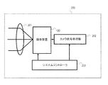
(第1の実施形態)
図1は、本開示の第1の実施形態による撮像装置の例示的な構成を示す。図1に示す撮像装置100Aは、複数の撮像セル10aを含む画素アレイPAと、周辺回路とを有する。撮像セル10aは、例えば半導体基板に2次元に配列されることにより、撮像領域を形成する。この例では、撮像セル10aが、m行n列のマトリクス状に配置されている。
(First embodiment)
FIG. 1 illustrates an exemplary configuration of an imaging apparatus according to the first embodiment of the present disclosure. An
図示する例において、各撮像セル10aの中心は、正方格子の格子点上に位置している。もちろん、撮像セル10aの配置は、図示する例に限定されず、例えば、各中心が、三角格子、六角格子などの格子点上に位置するように複数の撮像セル10aを配置してもよい。複数の撮像セル10aは、1次元に配列されてもよい。つまり、撮像セル10aの配置は、m行1列または1行n列であり得る。この場合、撮像装置100Aをラインセンサとして利用することができる。
In the illustrated example, the center of each
図1に例示する構成において、周辺回路は、行走査回路80、列回路82、信号処理回路84、出力回路86および制御回路88を含んでいる。周辺回路は、画素アレイPAが形成される半導体基板上に配置されていてもよいし、その一部が他の基板上に配置されていてもよい。
In the configuration illustrated in FIG. 1, the peripheral circuit includes a
行走査回路80は、リセット制御線Riおよびフィードバック制御線Fiとの接続を有する。リセット制御線Riおよびフィードバック制御線Fiは、画素アレイPAの各行に対応して設けられている。すなわち、複数の撮像セル10aのうち、第i行に属する、1以上の撮像セル10aは、リセット制御線Riおよびフィードバック制御線Fiに接続されている。ここでは、i=0〜m−1であり、mは1以上の整数である。
行走査回路80は、図1において不図示のアドレス制御線との接続を有する。アドレス制御線もリセット制御線Riおよびフィードバック制御線Fiと同様に、画素アレイPAの各行に対応して設けられ、第i行に属する、1以上の撮像セル10aに接続される。行走査回路80は、アドレス制御線に所定の電圧を印加することにより、撮像セル10aを行単位で選択し、信号電圧の読み出し、および、後述するリセット動作を行う。行走査回路80は、垂直走査回路とも呼ばれる。
The
列回路82は、画素アレイPAの各列に対応して設けられた出力信号線Sjとの接続を有する。ここでは、j=0〜n−1であり、nは1以上の整数である。複数の撮像セル10aのうち、第j列に属する、1以上の撮像セル10aは、出力信号線Sjに接続されており、行走査回路80によって行単位で選択された撮像セル10aからの出力信号は、出力信号線Sjを介して列回路82に読み出される。列回路82は、撮像セル10aから読み出された出力信号に対し、相関二重サンプリングに代表される雑音抑圧信号処理、アナログ−デジタル変換(AD変換)などを行う。
The
信号処理回路84は、撮像セル10aから取得された画像信号に各種の処理を施す。本明細書において、「画像信号」は、出力信号線Sjを介して読み出される信号のうち、画像の形成に用いられる出力信号を指す。後に詳しく説明するように、第1の実施形態では、高感度の状態とされた撮像セル10aからの画像信号(以下、「高感度信号」と呼ぶことがある。)の読み出しと、低感度の状態とされた撮像セル10aからの画像信号(以下、「低感度信号」と呼ぶことがある。)の読み出しとが実行される。信号処理回路84は、これらの高感度信号および低感度信号に基づき、広ダイナミックレンジ画像を形成する。信号処理回路84の出力は、出力回路86を介して撮像装置100Aの外部に読み出される。
The
制御回路88は、撮像装置100Aの例えば外部から与えられる指令データ、クロックなどを受け取り、撮像装置100A全体を制御する。制御回路88は、典型的にはタイミングジェネレータを有し、行走査回路80、列回路82などに駆動信号を供給する。
The
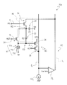
図2は、撮像セル10aの例示的な回路構成を示す。図2は、画素アレイPAの第i行に属する、第j列の撮像セル10aを取り出して示している。図2に示すように、撮像セル10aは、光電変換部11と、光電変換部11で発生した電気信号を検出する信号検出回路SCとを有する。
FIG. 2 shows an exemplary circuit configuration of the
信号検出回路SCは、第1容量素子21、リセットトランジスタ24および信号検出トランジスタ26を有する。この例では、信号検出回路SCは、アドレストランジスタ28を含んでいる。典型的には、リセットトランジスタ24、信号検出トランジスタ26およびアドレストランジスタ28は、半導体基板に形成された電界効果トランジスタ(FET)である。以下では、特に断りの無い限り、トランジスタとしてNチャンネルMOSを用いる例を説明する。なお、半導体基板は、その全体が半導体である基板に限定されず、撮像領域が形成される側の表面に半導体層が設けられた絶縁基板などであってもよい。
The signal detection circuit SC includes a
光電変換部11は、光の入射を受けて、照度に応じた信号を生成する。ここでは、光電変換部11として、画素電極11xおよび対向電極11zの間に光電変換層11yが挟まれた構造を例示する。この場合、典型的には、上述のリセットトランジスタ24などが形成される半導体基板上に層間絶縁層が設けられ、この層間絶縁層上に、光電変換部11が配置される。つまり、撮像装置100Aは、半導体基板の上部に光電変換層を有するいわゆる積層型の撮像装置であり得る。以下では、撮像装置100Aが積層型の撮像装置である例を説明する。もちろん、光電変換部11は、半導体基板に形成されたフォトダイオードなどであってもよい。その場合には、光電変換部11と、後述する電荷蓄積ノードFDとの間に転送トランジスタを設けてもよい。光電変換部11で発生した電荷が転送トランジスタを介して電荷蓄積ノードFDに転送された後は、以下の各実施形態で説明する動作を適用できる。
The
光電変換部11において、画素電極11xは、上述のリセットトランジスタ24などを覆う層間絶縁層上に配置される。画素電極11xは、撮像セル10aごとに設けられる。典型的には、各撮像セル10aの画素電極11xは、隣接する他の撮像セル10aの画素電極11xとの間で空間的に分離されることにより、他の撮像セル10aの画素電極11xから電気的に分離される。画素電極11xは、アルミニウム、銅などの金属、金属窒化物、または、不純物がドープされることにより導電性が付与されたポリシリコンなどから形成される。
In the
光電変換層11yは、有機材料またはアモルファスシリコンなどの無機材料から形成され、光電変換により、正および負の電荷(正孔−電子対)を生成する。典型的には、光電変換層11yは、複数の撮像セル10aにわたって形成される。光電変換層11yは、有機材料から構成される層と無機材料から構成される層とを含んでいてもよい。
The
光電変換層11yを介して画素電極11xに対向する対向電極11zは、ITOなどの透明な導電性材料から形成される電極であり、光電変換層11yの2つの主面のうち、光が入射する側に配置される。典型的には、対向電極11zは、光電変換層11yと同様に複数の撮像セル10aにわたって形成される。
The
撮像装置100Aの動作時、対向電極11zには所定の電圧Vpが印加される。複数の撮像セル10aにわたって対向電極11zを形成することにより、複数の撮像セル10aに一括して電圧Vpを印加することができる。電圧Vpとして、いくつかの撮像セル10aからなる画素ブロックごとに、異なる電圧を供給しても構わない。画素ブロックごとに異なる電圧を供給することにより、画素ブロックごとに感度を異ならせることができる。電圧Vpは、行走査回路80(図1参照)から供給されてもよいし、その他の電源回路から供給されてもよい。
During the operation of the
対向電極11zへの電圧Vpの印加により、光電変換層11yに生成された正孔および電子のうちの一方を画素電極11xによって収集することができる。信号電荷として正孔を利用する場合であれば、画素電極11xよりも対向電極11zの電位を高くすればよい。信号電荷として正孔を利用する場合、例えば、電圧Vpとして10V程度の電圧が対向電極11zに印加される。以下では、信号電荷として正孔を例示する。信号電荷として電子を利用してもよい。
By applying the voltage Vp to the
光電変換部11および信号検出回路SCは、層間絶縁層内に設けられた配線層によって電気的に接続される。図2に示すように、ここでは、画素電極11xと、信号検出トランジスタ26のゲートとが接続されている。画素電極11xによって収集された信号電荷は、画素電極11xおよび信号検出トランジスタ26のゲートの間のノードである電荷蓄積ノード(「フローティングディフュージョンノード」とも呼ばれる)FDに蓄積される。したがって、信号検出トランジスタ26のゲートには、電荷蓄積ノードFDに蓄積された信号電荷の量に応じた電圧が印加される。
The
信号検出トランジスタ26のソースは、アドレストランジスタ28を介して、出力信号線Sjに接続されている。出力信号線Sjは、上述の列回路82(図1参照)などから構成される定電流源CCjとの接続を有する。信号検出トランジスタ26のドレインは、電源配線(ソースフォロア電源)との接続を有する。信号検出トランジスタ26と、出力信号線Sjに接続された定電流源CCjとによって、ソースフォロア回路が形成される。撮像装置100Aの動作時、信号検出トランジスタ26は、ドレインに電源電圧VDD(例えば3.3V程度)の供給を受けることにより、ゲートに印加された電圧を増幅する。換言すれば、信号検出トランジスタ26は、光電変換部11によって生成された信号を増幅する。
The source of the
信号検出トランジスタ26によって増幅された電圧は、アドレストランジスタ28を介して信号電圧として選択的に読み出される。図示するように、アドレストランジスタ28のゲートは、画素アレイPAの行ごとに設けられるアドレス制御線Aiに接続される。アドレス制御線Aiは、典型的には、行走査回路80(図1参照)に接続されており、行走査回路80は、アドレス制御線Aiに印加する電圧ADの制御により、アドレストランジスタ28のオンおよびオフを制御することができる。
The voltage amplified by the
上述したように、信号検出回路SCは、第1容量素子21およびリセットトランジスタ24を有する。リセットトランジスタ24のソースおよびドレインのうちの一方(典型的にはドレイン)は、電荷蓄積ノードFDに接続されており、ソースおよびドレインのうちの他方は、第1容量素子21の一方の電極に接続されている。以下では、説明の便宜のため、リセットトランジスタ24と第1容量素子21との間のノードを「リセットドレインノードRD」と呼ぶことがある。
As described above, the signal detection circuit SC includes the
第1容量素子21の他方の電極には、撮像装置100Aの動作時、基準電位VR(例えば0V)が印加される。基準電位VRは、行走査回路80(図1参照)によって印加されてもよいし、その他の電源回路によって印加されてもよい。
A reference potential VR (for example, 0 V) is applied to the other electrode of the
第1容量素子21は、比較的大きな容量値C1を有する。第1容量素子21は、MIS(metal-insulator-semiconductor)構造を有していてもよいし、MIM(metal-insulator-metal)構造を有していてもよい。MIM構造を採用することにより、より大きな容量値を得やすい。なお、本明細書において、「容量素子(capacitor)」は、電極の間に絶縁膜などの誘電体が挟まれた構造を意味する。本明細書における「電極」は、金属から形成された電極に限定されず、ポリシリコン層などを広く含むように解釈される。本明細書における「電極」は、半導体基板の一部分であり得る。
The
図2に例示する構成において、信号検出回路SCは、リセットトランジスタ24に並列に接続された第2容量素子22をさらに含んでいる。なお、露光の回数を1回としながら低感度信号および高感度信号を個別に取得するという観点からは、第2容量素子22は、必須ではない。ただし、リセットトランジスタ24に並列に第2容量素子22を接続することにより、後述するノイズキャンセルの効果を向上させ得るので、ノイズ低減の観点からは、信号検出回路SCが第2容量素子22を有する方が有利である。
In the configuration illustrated in FIG. 2, the signal detection circuit SC further includes a
第2容量素子22の容量値C2は、第1容量素子21の容量値C1よりも小さい。容量値C2は、典型的には、容量値C1と比較して十分に小さい。第1容量素子21の容量値C1に対する、第2容量素子22の容量値C2の比(C2/C1)は、例えば、1/10程度であり得る。第2容量素子22の構造は、MIS構造およびMIM構造のいずれであってもよい。第1容量素子21の構造と第2容量素子22の構造とが一致している必要もない。
The capacitance value C2 of the
リセットトランジスタ24のゲートは、行走査回路80に接続されたリセット制御線Riに接続されている。したがって、行走査回路80は、リセット制御線Riに印加する電圧RSTの制御により、リセット制御線Riとの接続を有する撮像セル10aのリセットトランジスタ24におけるオンおよびオフを切り替えることができる。リセットトランジスタ24をオフとすることにより、撮像セル10a内において、第1容量素子21および第2容量素子22が直列に接続された容量回路を電荷蓄積ノードFDと基準電位VRとの間に形成することができる。後述するように、第1の実施形態では、1フレーム期間において、リセットトランジスタ24がオフの状態での信号の読み出し、および、リセットトランジスタ24がオンの状態での信号の読み出しを実行する。これにより、高感度信号および低感度信号を順次に取得することが可能である。なお、本明細書において、「順次に」とは、同時でないことを意味する。
The gate of the
この例では、撮像装置100Aは、フィードバック回路FCを有している。フィードバック回路FCは、出力信号線Sjに対応して画素アレイPAの例ごとに設けられた反転増幅器32jを含む。反転増幅器32jは、上述した周辺回路の一部であり得る。
In this example, the
図示するように、反転増幅器32jの反転入力端子は、第j列に属する1以上の撮像セル10aとの接続を有する出力信号線Sjに接続される。一方、非反転入力端子は、撮像装置100Aの動作時、所定の電圧(例えば1Vまたは1V近傍の正電圧)Vrefの供給を受ける。この電圧Vrefは、リセットにおける基準電圧として利用される。反転増幅器32jの出力端子は、フィードバック線Ljに接続される。
As illustrated, the inverting input terminal of the inverting
図示する例において、撮像セル10aは、ソースおよびドレインの一方がリセットドレインノードRDに接続されたフィードバックトランジスタ34を有する。フィードバック線Ljは、フィードバックトランジスタ34のソースおよびドレインの他方に接続される。図示するように、フィードバックトランジスタ34のゲートは、行走査回路80に接続されたフィードバック制御線Fiとの接続を有する。したがって、行走査回路80は、フィードバック制御線Fiに印加する電圧FBの制御により、フィードバックトランジスタ34におけるオンおよびオフを切り替えることができる。フィードバック制御線Fiに印加される電圧FBは、ハイレベルおよびローレベルの電圧に限定されず、傾斜電圧(rampvoltage)を含み得る。「傾斜電圧」は、時間の経過に伴って概ね増加または概ね減少する波形を有する電圧を広く含む。「傾斜電圧」は、直線状に増加または減少する電圧に限定されず、階段状の波形を有する電圧、振動を伴いながら増加または減少するような波形を有する電圧などであってもよい。
In the illustrated example, the
フィードバックトランジスタ34およびアドレストランジスタ28をオンとすることにより、光電変換部11で発生した電気信号を負帰還させる帰還経路を形成することができる。すなわち、フィードバック回路FCは、光電変換部11で発生した電気信号を、リセットトランジスタ24のソースおよびドレインのうち、電荷蓄積ノードFDに接続されていない側に負帰還させる回路であるといえる。フィードバックトランジスタ34および反転増幅器32jは、フィードバック回路FCにおける帰還経路の一部を構成する。反転増幅器32jをフィードバックアンプと呼んでもよい。
By turning on the
帰還経路の形成により、後述するノイズキャンセルを実行することが可能である。この例では、信号検出回路SCの出力を負帰還させるフィードバック回路FCは、フィードバックトランジスタ34、第1容量素子21および第2容量素子22を有する帯域制御回路40をその一部に含む。ノイズキャンセルにおいて、第1容量素子21およびフィードバックトランジスタ34は、RCフィルタ回路として機能する。なお、帰還経路の形成は、出力信号線Sjとの接続を有する1以上の撮像セル10aのうちの1つに対して順次に実行される。換言すれば、ノイズキャンセルの実行は、行単位である。
By forming the feedback path, it is possible to execute noise cancellation described later. In this example, the feedback circuit FC that negatively feeds back the output of the signal detection circuit SC includes a
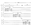
(第1の実施形態における信号読み出し動作)
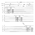
図3は、第1の実施形態における信号読み出し動作の典型例を説明するためのタイミングチャートである。図3中、RSTpsは、画素アレイPAの各行におけるリセットの開始のタイミングを指定する電圧パルスを示す。ADi、RSTiおよびFBiは、それぞれ、第i行のアドレス制御線Ai、リセット制御線Riおよびフィードバック制御線Fiに印加される電圧の変化を示す。以下において説明する動作は、行単位で露光および信号の読み出しを行ういわゆるローリングシャッタを適用した例である。図3中、網掛けの矩形HR、LRおよびRRは、それぞれ、高感度信号、低感度信号およびリセット信号の読み出しの期間を示している。両矢印NRCは、信号の取得後のリセットおよびノイズキャンセルのための期間を示す。リセットおよびノイズキャンセルの詳細は、後述する。
(Signal read operation in the first embodiment)
FIG. 3 is a timing chart for explaining a typical example of the signal read operation in the first embodiment. In FIG. 3, RSTps indicates a voltage pulse that specifies the reset start timing in each row of the pixel array PA. AD i , RST i, and FB i indicate changes in voltage applied to the address control line A i , reset control line R i, and feedback control line F i in the i-th row, respectively. The operation described below is an example in which a so-called rolling shutter that performs exposure and signal readout in units of rows is applied. In FIG. 3, hatched rectangles HR, LR, and RR indicate periods of reading out the high sensitivity signal, the low sensitivity signal, and the reset signal, respectively. A double-headed arrow NRC indicates a period for reset and noise cancellation after signal acquisition. Details of the reset and noise cancellation will be described later.
ここでは、第0行に注目する。露光および信号の読み出しに先立ち、まず、後述するリセット動作により、電荷蓄積ノードFDの電荷をリセットする。このとき、後述のノイズキャンセルを実行することによって、リセットにおいて発生したkTCノイズを低減する。リセットおよびノイズキャンセルの後、露光を開始する。第0行の露光期間において、AD0、RST0およびFB0は、いずれもローレベルである。すなわち、第0行に属する撮像セル10aのアドレストランジスタ28、リセットトランジスタ24およびフィードバックトランジスタ34は、いずれもオフの状態である。なお、図が複雑となることを避けるため、図3には、露光前のリセットおよびノイズキャンセル、および、その後の露光期間は示されていない。
Here, pay attention to the 0th row. Prior to exposure and signal readout, first, the charge of the charge storage node FD is reset by a reset operation described later. At this time, the kTC noise generated in the reset is reduced by executing noise cancellation described later. After reset and noise cancellation, exposure is started. In the exposure period of the 0th row, AD 0 , RST 0 and FB 0 are all at a low level. That is, the
露光により、電荷蓄積ノードFDを含む、信号電荷の蓄積領域(以下、「電荷蓄積領域」と呼ぶことがある)に、照度に応じた信号電荷(ここでは正孔)が蓄積される。露光期間の終了後、行走査回路80は、AD0をハイレベルに変更することにより、アドレストランジスタ28をオンする。アドレストランジスタ28がオンすることにより、信号検出トランジスタ26を介して、蓄積された電荷量に応じた信号が出力信号線Sjに読み出される。
By exposure, signal charges (here, holes) corresponding to the illuminance are accumulated in a signal charge accumulation region (hereinafter also referred to as “charge accumulation region”) including the charge accumulation node FD. After the end of the exposure period, the
この例では、まず、リセットトランジスタ24がオフの状態での信号の読み出しが実行される。リセットトランジスタ24がオフのとき、光電変換部11と基準電位との間に、第1容量素子21および第2容量素子22が直列に接続された容量回路が形成される。電荷蓄積ノードFDの寄生容量の容量値をCfdとすれば、リセットトランジスタ24がオフの状態における、電荷蓄積領域全体の容量値は、(Cfd+(C1C2)/(C1+C2))と表される。上述したように、第2容量素子22の容量値C2は、典型的には、第1容量素子21の容量値C1と比較して十分に小さい。したがって、リセットトランジスタ24がオフの状態における、信号電荷の蓄積領域全体の容量値は、おおよそ(Cfd+C2)である。
In this example, first, reading of a signal is executed in a state where the
第1の実施形態においては、リセットトランジスタ24がオフの状態で信号検出トランジスタ26を介して取得される画像信号が、上述の高感度信号に相当する。なお、画像信号の読み出し期間は、列回路82(図1参照)によるAD変換のための期間を含み得る。高感度信号に対応する画像データ(第1の画像データ)は、バッファメモリに一旦保存される。バッファメモリは、例えば、上述の列回路82内または信号処理回路84内に配置される。
In the first embodiment, an image signal acquired through the
第1の実施形態では、リセットトランジスタ24がオフの状態での画像信号の読み出し後、リセットトランジスタ24がオンの状態での画像信号の読み出しをさらに実行する。リセットトランジスタ24がオフの状態での画像信号の読み出し後、行走査回路80は、RST0をハイレベルに変更し、リセットトランジスタ24をオンとする。リセットトランジスタ24がオンとされることにより、第1容量素子21がリセットトランジスタ24を介して光電変換部11に接続される。第1容量素子21がリセットトランジスタ24を介して光電変換部11に接続されることにより、電荷蓄積領域全体の容量値が(Cfd+C2)から(Cfd+C1)に増大する。
In the first embodiment, after the image signal is read with the
リセットトランジスタ24をオンとした後、画像信号が読み出される。このとき、信号検出トランジスタ26を介して取得される画像信号が、上述の低感度信号に相当する。図2を参照すればわかるように、上述の高感度信号の読み出しは、電荷蓄積ノードFDからの信号電荷自体の取り出しを伴わない非破壊の読み出しである。なお、信号電荷は、高感度信号の読み出しの間においても蓄積されるが、画像信号の読み出しに必要な時間は、露光期間の全体に対して十分に短い。そのため、高感度信号と低感度信号との間で、露光期間の長さは、同じであるといってよい。したがって、高感度信号の読み出し時と、低感度信号の読み出し時との間で、電荷蓄積領域全体に蓄積されている電荷量にほとんど変化はない。
After the
ここでは、低感度信号の読み出し時における電荷蓄積領域全体の容量値が、高感度信号の読み出し時と比較して増大している。そのため、信号検出トランジスタ26のゲート電圧が低下し、同じ電荷蓄積量でありながら、出力される信号レベルが低下する。つまり、撮像セル10aの感度を低下させた状態での撮影と同様の状態が実現する。例えば、(Cfd+C2):(Cfd+C1)=1:10とすれば、リセットトランジスタ24がオフの状態(高感度の状態に相当)とリセットトランジスタ24がオンの状態(低感度の状態に相当)との間で、10:1の感度比を実現し得る。
Here, the capacitance value of the entire charge storage region at the time of reading out the low sensitivity signal is increased as compared with that at the time of reading out the high sensitivity signal. For this reason, the gate voltage of the
リセットトランジスタ24がオンの状態での低感度信号の読み出し後、再度リセットおよびノイズキャンセルを実行する。この例では、RST0およびFB0をハイレベルに変更することによってリセットトランジスタ24およびフィードバックトランジスタ34をオンとし、その後、リセットトランジスタ24をオフとすることによって、リセットが実行されている。第1の実施形態では、リセットトランジスタ24は、撮像セル10aから高感度信号および低感度信号のいずれを出力するかを切り替える機能と、電荷蓄積ノードFDのリセットを開始する機能とを有するといえる。
After reading out the low sensitivity signal with the
また、この例では、リセットトランジスタ24のオフに続けて、電圧FB0をハイレベルからローレベルまで低下させることによって、ノイズキャンセルが実行されている。リセットおよびノイズキャンセルの実行後、出力信号線Sjの電圧を読み出すことにより、リセット信号を取得する。リセット信号の読み出し期間は、AD変換のための期間を含み得る。リセット信号は、列回路82(図1参照)による相関二重サンプリングに利用される。相関二重サンプリングは、信号処理回路84によって実行されてもよい。
Further, in this example, the noise cancellation is executed by lowering the voltage FB 0 from the high level to the low level after the
図3に示すように、上述の一連の動作が行単位で実行される。最終行におけるリセット信号の読み出しの終了により、1フレーム期間が終了する。本明細書において、「1フレーム期間」は、最初の行(ここでは第0行)における高感度信号または低感度信号の読み出しから、最終行(ここでは第(m−1)行)におけるリセット信号の読み出しの終了までの期間として定義される。 As shown in FIG. 3, the above-described series of operations is executed in units of rows. One frame period ends when the reset signal reading in the last row ends. In this specification, “one frame period” refers to the reset signal in the last row (here, the (m−1) th row) from the readout of the high sensitivity signal or low sensitivity signal in the first row (here, the 0th row). Is defined as the period until the end of reading.
なお、図3に示す例では、低感度信号の読み出し後、リセットトランジスタ24を一旦オフとしてから再度オンとしている。すなわち、ここでは、1フレーム期間において、撮像セル10aの各々におけるリセットトランジスタ24のオンが2回(オフが2回といってもよい。)であるような制御が実行されている。このように、撮像セル10aの各々におけるリセットトランジスタ24を、1フレーム期間において少なくとも2回オンまたはオフさせるような制御が実行されてもよい。あるいは、低感度信号の読み出し後、リセットトランジスタ24をオフとせずにフィードバックトランジスタ34をオンすることによってリセットを開始してもよい。リセットトランジスタ24およびフィードバックトランジスタ34におけるオンおよびオフは、例えば上述の制御回路88(図1参照)の制御に基づいて実行される。
In the example shown in FIG. 3, after the low sensitivity signal is read, the
高感度信号に対応する画像データ(第1の画像データ)と、低感度信号に対応する画像データ(第2の画像データ)とを合成することにより、白飛びおよび黒潰れの抑制された画像(広ダイナミックレンジ画像)を形成することが可能である。このような画像の形成は、「ハイダイナミックレンジ合成」と呼ばれる。ハイダイナミックレンジ合成の具体的な方法としては、公知の方法を適用可能である。第1の画像データおよび第2の画像データの合成は、例えば信号処理回路84によって実行される。なお、第1の画像データと、第2の画像データとの合成は、行単位で実行されてもよいし、フレーム単位で実行されてもよい。行単位での合成を実行すれば、高感度信号の読み出しと低感度信号の読み出しとの間の時間差を、1H期間(1行の走査に要する時間)分の長さに抑制できる。
By combining the image data corresponding to the high sensitivity signal (first image data) and the image data corresponding to the low sensitivity signal (second image data), an image in which whiteout and blackout are suppressed ( Wide dynamic range image) can be formed. Such image formation is called “high dynamic range synthesis”. A known method can be applied as a specific method of high dynamic range synthesis. The synthesis of the first image data and the second image data is executed by the
このように、第1の実施形態では、各撮像セル10aの各々は、1フレーム期間において高感度信号および低感度信号を順次に出力する。上述の説明から明らかなように、第1の実施形態によれば、1フレーム期間における各撮像セル10aへの露光が1回でありながら、各撮像セル10aから、高感度信号と低感度信号とを個別に取得することができる。換言すれば、高感度信号の取得および低感度信号の取得のそれぞれのために合計2回の露光期間を設定する必要がない。したがって、広ダイナミックレンジ画像における画質の劣化の発生が抑制される。また、動作の高速化が可能である。高感度信号および低感度信号の取得のたびにリセット動作を行う必要もない。
Thus, in the first embodiment, each of the
さらに、同じ行に属する撮像セル10aの各々に着目すると、高感度信号の取得のための露光期間の開始のタイミングおよび低感度信号の取得のための露光期間の開始のタイミングは、一致しており、かつ、これらの露光期間の長さは、ほぼ同じである。したがって、第1の実施形態によれば、高感度信号に対応する画像データと低感度信号に対応する画像データとの間における同時性を確保し得る。
Further, focusing on each of the
(リセットおよびノイズキャンセル)
ここで、図2および図3を参照しながら、リセットおよびノイズキャンセルにおける動作の詳細を説明する。上述したように、リセットトランジスタ24およびフィードバックトランジスタ34をオンとすることにより、リセットが開始される。図2からわかるように、リセットトランジスタ24およびフィードバックトランジスタ34をオンとすることにより、電荷蓄積ノードFDとフィードバック線Ljとがリセットトランジスタ24およびフィードバックトランジスタ34を介して接続され、光電変換部11の信号をフィードバック(ここでは負帰還)させる帰還経路が形成される。フィードバックトランジスタ34は、帰還経路を形成するか否かを切り替える機能を有する。帰還経路の形成は、出力信号線Sjに接続された撮像セル10aのうち、アドレス制御線Aiの電圧ADiがハイレベルとされることにより選択された行の撮像セル10aに対して実行される。
(Reset and noise cancellation)
Here, with reference to FIG. 2 and FIG. 3, details of operations in reset and noise cancellation will be described. As described above, the reset is started by turning on the
電荷蓄積ノードFDとフィードバック線Ljとが電気的に接続されることにより、出力信号線Sjの電圧が、反転増幅器32jの非反転入力端子に印加された電圧Vrefに収束する。電圧Vrefとしては、電源電圧(例えば3.3V)および接地(0V)の範囲内の任意の大きさの電圧を用い得る。
By electrically connecting the charge storage node FD and the feedback line L j , the voltage of the output signal line S j converges to the voltage Vref applied to the non-inverting input terminal of the inverting
次に、リセットトランジスタ24をオフとする。リセットトランジスタ24をオフとすることによりkTCノイズが発生する。したがって、リセット後における電荷蓄積ノードFDの電圧に、kTCノイズが加わる。
Next, the
図2を参照すればわかるように、フィードバックトランジスタ34がオンである間は、電荷蓄積ノードFD、信号検出トランジスタ26、フィードバックトランジスタ34および第2容量素子22をその経路に含む帰還経路が形成された状態が継続している。帰還経路が形成されている時(フィードバックトランジスタ34がオフではない時といってもよい)、フィードバックトランジスタ34が出力する信号は、第2容量素子22と電荷蓄積ノードFDの寄生容量とによって形成される減衰回路で減衰される。このときの減衰率Bは、B=C2/(C2+Cfd)と表される。そのため、フィードバック回路FCの利得をAとすれば、リセットトランジスタ24をオフとすることによって生じたkTCノイズは、1/(1+A×B)倍に抑制される。
As can be seen from FIG. 2, while the
この例では、リセットトランジスタ24をオフとする直前(ノイズキャンセル開始の直前)における出力信号線Sjの電圧は、反転増幅器32jの非反転入力端子に印加された電圧Vrefにほぼ等しい。このように、ノイズキャンセル開始時における出力信号線Sjの電圧をノイズキャンセル後の目標電圧Vrefに近づけておくことにより、比較的短い時間でkTCノイズをキャンセルすることができる。
In this example, the voltage of the output signal line S j immediately before turning off the reset transistor 24 (immediately before the start of noise cancellation) is substantially equal to the voltage Vref applied to the non-inverting input terminal of the inverting
ここでは、リセットトランジスタ24をオフとした直後におけるフィードバック制御線Fiの電圧レベルは、ハイレベルである。したがって、リセットトランジスタ24をオフとした直後におけるフィードバックトランジスタ34の動作帯域が比較的広帯域である。フィードバックトランジスタ34の動作帯域が広いと、ノイズを高速に抑制することが可能である。
Here, the voltage levels of the feedback control line F i in immediately after turning off the
さらにここでは、リセットトランジスタ24をオフとした後、フィードバック制御線Fiの電圧レベルをハイレベルからローレベルまで徐々に低下させている。フィードバックトランジスタ34のしきい値電圧を跨ぐように、フィードバック制御線Fiの電位をハイレベルからローレベルに向けて徐々に低下させると、フィードバックトランジスタ34は、オン状態からオフ状態に徐々に変化する。このとき、フィードバック制御線Fiに印加されている電圧FBiの低下に伴って、フィードバックトランジスタ34の抵抗が増加する。フィードバックトランジスタ34の抵抗が増加すると、フィードバックトランジスタ34の動作帯域が狭くなり、帰還する信号の周波数領域が狭くなる。フィードバックトランジスタ34の動作帯域を信号検出トランジスタ26の動作帯域よりも十分に低い帯域とすることにより、ノイズ抑制効果を向上させることができる。
Furthermore Here, after turning off the
フィードバック制御線Fiに印加されている電圧FBiがローレベルに達すると、フィードバックトランジスタ34がオフとなる。つまり、帰還経路の形成が解消される。フィードバックトランジスタ34の動作帯域が、信号検出トランジスタ26の動作帯域よりも十分に低い帯域であると、フィードバックトランジスタ34で発生する熱ノイズは、フィードバック回路FCにより、1/(1+A×B)1/2倍に抑制される。フィードバックトランジスタ34の動作帯域が信号検出トランジスタ26の動作帯域よりも低い状態でフィードバックトランジスタ34をオフとすることにより、電荷蓄積ノードFDに残存するkTCノイズを低減することが可能である。
When the voltage FB i applied to the feedback control line F i reaches a low level, the
このように、フィードバック回路FCを設けることにより、kTCノイズを低減することができる。したがって、ノイズの影響が抑制された広ダイナミックレンジ画像を得ることができる。また、第1容量素子21を、感度の異なる状態に対応した2つの信号(高感度信号および低感度信号)の取得だけでなく、ノイズキャンセルにも有効に利用することができる。なお、当業者であれば容易に理解されるように、第2容量素子22を省略した回路構成によっても、高感度信号と低感度信号との間の切り替え自体は可能である。ただし、十分に小さな容量値を有する第2容量素子22を用いることにより、減衰率Bとしてより大きな値が得られるので、より効果的にノイズをキャンセルし得る。
Thus, kTC noise can be reduced by providing the feedback circuit FC. Therefore, it is possible to obtain a wide dynamic range image in which the influence of noise is suppressed. Further, the
(第1の実施形態の変形例)
図4は、第1の実施形態による撮像装置の変形例を示す。図4に示す撮像装置100Bと、図1〜図3を参照して説明した撮像装置100Aの相違点は、撮像装置100Bが、撮像セル10aに加えて、撮像セル10aよりも感度の低い第2の撮像セル10bを有する点である。以下に説明するように、撮像セル10aおよび撮像セル10bを用いることにより、よりダイナミックレンジの広いシーンの撮影が容易になる。以下では、撮像セル10bを低感度セル10bと呼ぶ。
(Modification of the first embodiment)
FIG. 4 shows a modification of the imaging apparatus according to the first embodiment. The difference between the
図4に例示する構成では、撮像セル10aおよび低感度セル10bが行方向に沿って隣接している。本明細書において、行方向は、行が延びる方向を意味し、列方向は、列が延びる方向を意味する。つまり、例えば図1において、紙面における垂直方向が列方向であり、紙面における水平方向が行方向である。この例では、同一の行において隣接する撮像セル10aおよび低感度セル10bが、セル対10Pを構成している。複数のセル対10Pが例えば半導体基板にマトリクス状に配列されることにより、撮像装置100Bにおける撮像領域が形成される。図4は、撮像装置100Bの画素アレイPAの第i行に属するセル対10Pのうちの1つである第j列のセル対10Pにおける回路構成の典型例を示している。なお、撮像セル10aおよび低感度セル10bを列方向に沿って隣接するように配置することにより、セル対10Pを形成してもよい。
In the configuration illustrated in FIG. 4, the
低感度セル10bは、概略的には、上述した撮像セル10aに似た構成を有する。図4に示すように、低感度セル10bは、光電変換部12bと、光電変換部12bで発生した電気信号を検出する信号検出回路SCbとを有する。
The
信号検出回路SCbは、光電変換部12bおよび基準電位VRの間に接続された第3容量素子23bと、信号検出トランジスタ26bとを有する。図4に示す例では、信号検出回路SCbは、アドレストランジスタ28bをさらに含んでいる。アドレストランジスタ28bは、信号検出トランジスタ26bのソースまたはドレインの一方(ここではソース)と、列回路82(図1参照)に接続された出力信号線Sbjとの間に接続されている。
The signal detection circuit SCb includes a
光電変換部12bは、撮像セル10aにおける光電変換部11と同様の構成を有し得る。ここでは、光電変換部12bとして、光電変換部11と同様に、画素電極12xおよび対向電極12zの間に光電変換層12yが挟まれた構造を例示する。
The
画素電極12xは、典型的には、信号検出トランジスタ26b、アドレストランジスタ28bなどを覆う層間絶縁層上に配置される。画素電極12xは、空間的に分離されることにより、隣接する他の画素電極11xおよび画素電極12xから電気的に分離されている。他方、典型的には、低感度セル10bにおける光電変換層12yおよび撮像セル10aにおける光電変換層11yのそれぞれは、連続する単一の光電変換層の一部である。また、典型的には、低感度セル10bにおける対向電極12zおよび撮像セル10aにおける対向電極11zのそれぞれは、連続する単一の電極の一部である。
The
撮像装置100Bの動作時、低感度セル10bにおける対向電極12zには、撮像セル10aにおける対向電極11zと同様に、所定の電圧Vpが印加される。対向電極12zに所定の電圧Vpを印加することにより、光電変換層12yにおいて発生した正および負の電荷のうちの一方を画素電極12xによって収集することができる。電圧Vpとして、いくつかのセル対10Pからなる画素ブロックごとに、異なる電圧を供給してもよい。
During the operation of the
図4に示すように、画素電極12xは、信号検出トランジスタ26bのゲートとの接続を有する。画素電極12xおよび信号検出トランジスタ26bのゲートの間のノードである電荷蓄積ノードFDbは、信号電荷が蓄積される電荷蓄積領域の少なくとも一部を構成する。したがって、信号検出トランジスタ26bのゲートには、電荷蓄積ノードFDbに蓄積された信号電荷の量に応じた電圧が印加される。
As shown in FIG. 4, the
図4に示すように、低感度セル10bは、一方の電極が電荷蓄積ノードFDbに接続された第3容量素子23bを有する。第3容量素子23bは、撮像セル10aにおける第1容量素子21と同様に、比較的大きな容量値C3を有する。典型的には、第3容量素子23bの容量値C3は、第1容量素子21の容量値C1と同等かそれ以上である。この例では、光電変換部12bと第3容量素子23bとの間には、トランジスタは接続されていない。
As shown in FIG. 4, the
容量値C3の具体的な値は、低感度セル10bが、リセットトランジスタ24がオンとされた状態、換言すれば、低感度状態にある撮像セル10aよりも低い感度を有するように設定される。後述するように、撮像装置100Bでは、リセットトランジスタ24がオフとされた状態の撮像セル10a、リセットトランジスタ24がオンとされた状態の撮像セル10aおよび低感度セル10bを、それぞれ、最も感度の高いセル、中程度の感度のセルおよび最も感度の低いセルとして利用する。広ダイナミックレンジ画像のある画素における輝度値は、これらのセルから取得される、互いに感度の異なる3つの画像信号から選択された1つに基づいて決定される。
The specific value of the capacitance value C3 is set such that the
信号検出トランジスタ26bのソースまたはドレインのうち、アドレストランジスタ28bに接続されていない側(ここではドレイン)は、電源配線(ソースフォロア電源)に接続されており、撮像装置100Bの動作時に電源電圧VDDの供給を受ける。信号検出トランジスタ26bと、出力信号線Sbjに接続された定電流源CCbjとによって、ソースフォロア回路が形成される。すなわち、信号検出トランジスタ26bは、光電変換部12bによって生成された信号を増幅する。
Of the source or drain of the
アドレストランジスタ28bをオンとすることにより、信号検出トランジスタ26bによって増幅された信号を、定電流源CCbjとの接続を有する出力信号線Sbjに読み出すことができる。図示するように、アドレストランジスタ28bのゲートには、アドレス制御線Abiが接続されている。アドレス制御線Abiは、典型的には、行走査回路80(図1参照)に接続される。アドレス制御線Abiに印加する電圧ADbを制御することにより、低感度セル10bを行単位で選択して信号を読み出すことができる。アドレス制御線Abiは、撮像セル10aのアドレストランジスタ28のゲートに接続されたアドレス制御線Aiと共通の信号線であり得る。
By turning on the
図4に例示する構成において、撮像装置100Bは、光電変換部12bで発生した電気信号を負帰還させる帰還経路を形成するフィードバック回路FCbを有する。図示するように、フィードバック回路FCbは、反転入力端子が出力信号線Sbjに接続され、出力端子がフィードバック線Lbiに接続された反転増幅器32bjを含む。フィードバック線Lbiと電荷蓄積ノードFDbとの間には、フィードバックトランジスタ34bが接続される。
In the configuration illustrated in FIG. 4, the
フィードバックトランジスタ34bのゲートは、フィードバック制御線Fbiに接続されている。フィードバック制御線Fbiに印加する電圧FBbを制御してフィードバックトランジスタ34bをオンとすることにより、フィードバックトランジスタ34bおよび反転増幅器32bjをその経路の一部に含む帰還経路を形成することができる。フィードバック制御線Fbiは、撮像セル10aのフィードバックトランジスタ34のゲートに接続されたフィードバック制御線Fiと共通の信号線であり得る。
The gate of the
低感度セル10bのリセットおよびノイズキャンセルにおけるフィードバック制御線Fbiの電位の制御は、図3を参照して説明した、撮像セル10aのリセットおよびノイズキャンセルにおけるフィードバック制御線Fiの電位の制御とほぼ同様であり得る。低感度セル10bにおけるリセットは、フィードバックトランジスタ34bをオンすることによって開始する。例えば、ハイレベルからローレベルに向かって低下するようにフィードバック制御線Fbiの電位を制御することにより、フィードバックトランジスタ34bのオフに伴って発生するkTCノイズを縮小することが可能である。なお、低感度セル10bの感度は、低感度状態にある撮像セル10aよりもさらに低くされているので、低感度セル10bにおけるkTCノイズの影響は、撮像セル10aにおけるkTCノイズの影響よりも小さい。したがって、低感度セル10bでは、撮像セル10aよりも強力なノイズキャンセルを行う必要性は低い。ある態様では、フィードバック回路FCbは、省略され得る。
The control of the potential of the feedback control line Fb i in the reset and noise cancellation of the low-
低感度セル10bにおける信号の読み出しのタイミングは、図3を参照して説明した、撮像セル10aにおける信号の読み出しのタイミングとほぼ同様であり得る。ただし、1フレーム期間における各低感度セル10bからの画像信号の読み出しは、1回である。低感度セル10bの感度は、低感度状態にある撮像セル10aよりもさらに低くされているので、説明の便宜のため、以下では、低感度セル10bから得られる画像信号を超低感度信号と呼ぶ。
The signal readout timing in the low-
撮像装置100Bでは、撮像セル10aおよび低感度セル10bのそれぞれに対する1回の露光で、高感度信号、低感度信号および超低感度信号の3つの信号を取得可能である。すなわち、撮像セルの種類が2つでありながら、高感度、低感度、より低感度の3つのセルを配置したときと同様の効果が得られる。高感度信号、低感度信号および超低感度信号を利用してハイダイナミックレンジ合成を実行することにより、より広いワイドダイナミックレンジを有するシーンを撮影した場合であっても、白飛びおよび黒潰れの抑制された画像を形成し得る。
In the
例えば、低感度セル10bにおける電荷蓄積ノードFDbの寄生容量の容量値を、撮像セル10aにおける電荷蓄積ノードFDの寄生容量のCfdに等しいとし、C3=C1=Csであるとする。この場合、低感度セル10bにおける電荷蓄積領域全体の容量値(Cfd+Cs)は、リセットトランジスタ24のオン時における撮像セル10aの電荷蓄積領域全体の容量値(Cfd+Cs)に等しい。ここで、低感度セル10bの光電変換部12bの画素電極12xの面積と、撮像セル10aの光電変換部11の画素電極11xの面積との間の比が1:10であったとすると、低感度セル10bと、リセットトランジスタ24のオン時の撮像セル10aとの間の感度比は、およそ1:10である。ここで、撮像セル10aにおいて、リセットトランジスタ24のオン時における電荷蓄積領域全体の容量値(Cfd+Cs)と、オフ時における電荷蓄積領域全体の容量値(Cfd+C2)との比が10:1であったとすれば、リセットトランジスタ24のオン時の撮像セル10aと、オフ時の撮像セル10aとの間の感度比は、およそ1:10である。結果として、このとき、低感度セル10b、リセットトランジスタ24のオン時の撮像セル10aおよびリセットトランジスタ24のオフ時の撮像セル10aの間で1:10:100の感度比が得られる。したがって、低感度セル10bを用いない場合よりもさらに広いダイナミックレンジを実現できる。なお、撮像装置100Bの動作時に、低感度セル10bにおける対向電極12zと撮像セル10aにおける対向電極11zとの間で互いに異なる電圧を供給することにより、低感度セル10bと撮像セル10aとの間に感度差を与えてもよい。
For example, assume that the capacitance value of the parasitic capacitance of the charge storage node FDb in the
図4に例示する構成では、撮像装置100Bがフィードバック回路FCbを有するので、超低感度信号へのkTCノイズの影響を低減し得る。さらに、撮像装置100Bでは、超低感度の画像データが低感度セル10bによって取得され、高感度の画像データおよび低感度の画像データが、より強力なノイズキャンセルを実行可能な撮像セル10aによって取得されるので、効果的に低ノイズ広ダイナミックレンジ画像の形成が可能である。
In the configuration illustrated in FIG. 4, since the
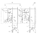
(第2の実施形態)
図5は、本開示の第2の実施形態による撮像装置の例示的な構成を示す。図5に示す撮像装置100Cと、図1に示す撮像装置100Aとの主な相異点は、撮像装置100Cにおける画素アレイPAが、感度切り替えレジスタ90に接続された複数の撮像セル10cを含む点である。この例では、感度切り替えレジスタ90が、列回路82B内に配置されている。
(Second Embodiment)
FIG. 5 illustrates an exemplary configuration of an imaging apparatus according to the second embodiment of the present disclosure. The main difference between the
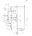
複数の撮像セル10cのうち、第i行に属する、1以上の撮像セル10cは、図1に示す撮像セル10aと同様に、画素アレイPAの各行に対応して設けられたリセット制御線Riおよびフィードバック制御線Fiに接続されている。複数の撮像セル10cのうち、第j列に属する、1以上の撮像セル10cは、図1に示す撮像セル10aと同様に、画素アレイPAの各列に対応して設けられた出力信号線Sjに接続されている。ここでは、第j列に属する、1以上の撮像セル10cは、さらに、画素アレイPAの各列に対応して設けられた感度切り替え線Bjにも接続されている。図示するように、感度切り替え線Bjは、列回路82Bに接続されている。
Among the plurality of
後に詳しく説明するように、第2の実施形態では、感度切り替え線Bjの電圧レベルを変更することにより、対応する撮像セル10cから、高感度信号および低感度信号のいずれを読み出すかを切り替える。感度切り替え線Bjの電圧レベルは、出力信号線Sjを介して読み出される電圧と参照電圧との比較によって決定される。換言すれば、各撮像セル10cからの画像信号の読み出し時における感度が、露光によって蓄積された信号電荷量に応じて動的に変更される。1フレーム期間において各撮像セル10cから読み出される画像信号は、高感度信号および低感度信号のいずれか一方であり、したがって、同一の行に属する撮像セル10cにおいて、高感度信号と低感度信号との間で露光期間の長さを揃えることができる。また、1フレーム期間において、各撮像セル10cからは高感度信号および低感度信号のいずれか一方が選択的に読み出されるので、1フレーム分の高感度の画像データおよび1フレーム分の低感度の画像データの間の合成処理が基本的に不要である。
As will be described in detail later, in the second embodiment, the voltage level of the sensitivity switching line B j is changed to switch which of the high sensitivity signal and the low sensitivity signal is read out from the corresponding
図6は、撮像セル10cの例示的な回路構成を示す。概略的には、撮像セル10cは、図2を参照して説明した撮像セル10aと同様の構成を有する。すなわち、撮像セル10cは、光電変換部11と、光電変換部11で発生した電気信号を検出する信号検出回路SCcとを有している。ただし、撮像セル10cにおける信号検出回路SCcは、リセットドレインノードRDに感度切り替えトランジスタ36を含んでいる。
FIG. 6 shows an exemplary circuit configuration of the
感度切り替えトランジスタ36は、リセットトランジスタ24のソースおよびドレインのうち光電変換部11に接続されていない側と、第1容量素子21の電極のうち撮像装置100Cの動作時に基準電位が印加されない側の電極との間に接続される。感度切り替えトランジスタ36のゲートには、対応する感度切り替え線Bjが接続される。例えば、第0列に属する撮像セル10cの感度切り替えトランジスタ36であれば、そのゲートに感度切り替え線B0が接続される。
The
既に説明したように、第1の実施形態では、リセットトランジスタ24のゲートに印加する電圧レベルを切り替えることによって、撮像セル10aから読み出すべき画像信号を高感度信号および低感度信号の間で切り替える。第1の実施形態では、高感度信号および低感度信号が順次に読み出される。これに対し、第2の実施形態では、感度切り替え線Bjを介して、感度切り替えトランジスタ36のゲートに印加する電圧レベルを制御することにより、高感度信号および低感度信号のいずれか一方を選択し、その画像信号を1フレーム期間において読み出す。
As already described, in the first embodiment, the image signal to be read from the
図7は、感度切り替えレジスタ90の回路構成の典型例を示す。図7に模式的に示すように、感度切り替えレジスタ90は、画素アレイPAの各列に対応して設けられた、比較器Cmpj、レジスタRgjおよびORゲートGtjから構成される複数のセットを含む。図7においては、m個のセットのうち、第0列、第1列、第2列および第(m−1)列に対応する4つのセットを代表として示している。説明の便宜のために、図7においては、画素アレイPAに含まれる複数の撮像セル10cのうち、ある行に属する撮像セル10cも示されている。
FIG. 7 shows a typical example of the circuit configuration of the
図示するように、感度切り替えレジスタ90中の各比較器Cmpjは、参照電圧線50に接続されている。参照電圧線50は、不図示の電圧源との接続を有し、撮像装置100C動作時に、所定の参照電圧REFが印加される。参照電圧REFとしては、例えば、電荷蓄積ノードFDにおいて電荷のオーバーフローが生じるかどうかの判断の基準となる動作限界電圧を用いることができる。
As illustrated, each comparator Cmp j in the
第j列の比較器Cmpjは、対応する出力信号線Sjに接続されている。比較器Cmpjは、出力信号線Sjの電圧と参照電圧REFとを比較し、対応するレジスタRgjにその結果を返す。比較器Cmpjは、例えば、出力信号線Sjの電圧が参照電圧REFを上回っている場合にハイレベルの信号を出力する。 The comparator Cmp j in the j-th column is connected to the corresponding output signal line S j . The comparator Cmp j compares the voltage of the output signal line S j with the reference voltage REF and returns the result to the corresponding register Rg j . For example, the comparator Cmp j outputs a high-level signal when the voltage of the output signal line S j exceeds the reference voltage REF.
レジスタRgjは、出力信号線Sjの電圧と参照電圧REFとの比較結果を一時的に保持する。例えば、出力信号線Sjの電圧が参照電圧REFを上回っている場合に「1」がセットされ、出力信号線Sjの電圧が参照電圧REFを上回っていない場合に「0」がセットされる。なお、図7に例示する構成では、各レジスタRgjは、レジスタリセット信号線52にも接続されている。レジスタリセット信号線52に所定の信号を供給することにより、各レジスタRgjを初期状態にリセットすることができる。例えば、レジスタリセット信号線52に印加される電圧RGrstをローレベルとすることにより、各レジスタRgjに保持された比較結果を「0」にリセットする。
The register Rg j temporarily holds the comparison result between the voltage of the output signal line S j and the reference voltage REF. For example, "1" if the voltage of the output signal line S j is higher than the reference voltage REF is set, "0" is set when the voltage of the output signal line S j does not exceed the reference voltage REF . In the configuration illustrated in FIG. 7, each register Rg j is also connected to the register
ORゲートGtjは、レジスタRgjに保持された比較結果と、画素アレイPAの各行におけるリセットの開始のタイミングを指定する電圧パルスを供給するリセット信号線54の電圧レベルとの論理和を感度切り替え線Bjに出力する。例えば、図7において、レジスタRg0には「0」が保持されているので、リセット信号線54の電圧レベルがローレベル時、対応する感度切り替え線B0の電圧レベルがローレベルとなる。感度切り替え線B0の電圧レベルがローレベルであるので、第0列に属する1以上の撮像セル10cにおける、感度切り替えトランジスタ36がオフとなる。このとき、光電変換部11および第1容量素子21が第2容量素子22を介して接続され(図6参照)、撮像セル10cが高感度の状態となる。つまり、感度切り替え線Bjの電圧レベルがローレベルのとき、対応する撮像セル10cから高感度信号が読み出される。
The OR gate Gt j switches sensitivity of the comparison result held in the register Rg j and the voltage level of the
他方、レジスタRg1には「1」が保持されているので、対応する感度切り替え線B1の電圧レベルは、ハイレベルである。したがって、第1列に属する1以上の撮像セル10cにおける、感度切り替えトランジスタ36がオンとなる。リセットトランジスタ24がオンであると、リセットトランジスタ24および感度切り替えトランジスタ36を介して光電変換部11と第1容量素子21とが接続され(図6参照)、電荷蓄積領域全体の容量値が増大する。したがって、第1列に属する1以上の撮像セル10cから読み出される画像信号は、低感度信号となる。このように、感度切り替え線Bjの電圧レベルがハイレベルのとき、対応する撮像セル10cから低感度信号が読み出される。
On the other hand, since “1” is held in the register Rg 1 , the voltage level of the corresponding sensitivity switching line B 1 is high. Therefore, the
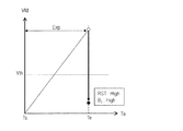
図8および図9は、露光による電荷蓄積ノードFDの電圧の変化に応じた撮像セル10cにおける感度の切り替えを説明するための図である。図8および図9は、それぞれ、図7に示す第0列および第1列における、露光時間(信号電荷蓄積の時間)と、電荷蓄積ノードFDの電圧(蓄積された信号電荷量あるいは信号検出トランジスタ26のゲート電圧といってもよい)との間の関係を模式的に示している。図8および図9に示されるグラフの横軸および縦軸は、それぞれ、露光時間Taおよび電荷蓄積ノードFDの電圧Vfdを示す。横軸におけるTsおよびTeは、露光の開始および終了のタイミングをそれぞれ示し、縦軸におけるVthは、上述の動作限界電圧を示す。グラフ中の両矢印Expは、露光期間を示す。
8 and 9 are diagrams for explaining sensitivity switching in the
図8に示すように、第0列の撮像セル10cでは、電荷蓄積ノードFDの電圧Vfdは、露光期間Expの全体において動作限界電圧Vthを下回っている。そのため、対応する感度切り替え線B0の電圧レベルは、ローレベルである。したがって、第0列では、電圧Vfdに応じた画像信号がそのまま出力信号線S0に出力される。換言すれば、撮像セル10cからは、高感度信号が読み出される。他方、第1列の撮像セル10cでは、図9に示すように、露光期間中のある時点以降、電荷蓄積ノードFDの電圧Vfdが動作限界電圧Vthを上回っている。そのため、対応する感度切り替え線B1の電圧レベルがハイレベルとなり、感度切り替えトランジスタ36がオンとなる。
As shown in FIG. 8, in the
リセットトランジスタ24のオン時に感度切り替えトランジスタ36がオンとなることにより、感度切り替えトランジスタ36を介して光電変換部11と第1容量素子21とが接続される。リセットトランジスタ24および感度切り替えトランジスタ36のいずれかがオフであれば、電荷蓄積領域全体の容量値は、(Cfd+C2)であり、リセットトランジスタ24および感度切り替えトランジスタ36の両方がオンであれば、電荷蓄積領域全体の容量値は、(Cfd+C1)である。したがって、リセットトランジスタ24のオン時に感度切り替えトランジスタ36がオフからオンとなることによって、電荷蓄積領域全体の容量値が(Cfd+C2)から(Cfd+C1)に増大する。例えば(Cfd+C2):(Cfd+C1)=1:10であったとすると、感度切り替えトランジスタ36がオンとなることにより、下向きの矢印によって模式的に示すように、電圧Vfdが(1/10)程度に低下する。すなわち、撮像セル10cからは、低感度信号が読み出される。
Since the
図10は、第2の実施形態における信号読み出し動作の典型例を説明するためのタイミングチャートである。図10中、RGrstは、レジスタリセット信号線52に印加される電圧の変化を示す。BSiは、第i行に属する撮像セル10cの感度切り替えトランジスタ36のゲートに感度切り替え線Bjを介して印加される電圧の変化を示す。ADi、RSTiおよびFBiは、図3と同様に、それぞれ、第i行のアドレス制御線Ai、リセット制御線Riおよびフィードバック制御線Fiに印加される電圧の変化を示す。図10中、網掛けの矩形RRは、図3と同様に、リセット信号の読み出しの期間を示し、両矢印NRCは、信号の取得後のリセットおよびノイズキャンセルのための期間を示す。
FIG. 10 is a timing chart for explaining a typical example of the signal read operation in the second embodiment. In FIG. 10, RGrst indicates a change in voltage applied to the register
第0行に注目する。露光および信号の読み出しに先立ち、まず、上述したリセットおよびノイズキャンセルを実行する。リセットおよびノイズキャンセルの後、露光を開始する。ここで説明する動作例では、露光前において、初期値として、各列のレジスタRgjに「0」がセットされているとする。
Pay attention to
第0行の露光期間において、AD0、RST0およびFB0は、いずれもローレベルである。すなわち、第0行に属する撮像セル10aのアドレストランジスタ28、リセットトランジスタ24およびフィードバックトランジスタ34は、いずれもオフの状態である。また、各列のレジスタRgjに「0」がセットされているので、各列の感度切り替え線Bjの電圧レベルは、ローレベルであり、感度切り替えトランジスタ36もオフの状態である。
In the exposure period of the 0th row, AD 0 , RST 0 and FB 0 are all at a low level. That is, the
露光による電荷蓄積領域への信号電荷の蓄積の終了後、第0行のアドレストランジスタ28をオンとする。これにより、蓄積された電荷量に応じた信号が各列の出力信号線Sjに読み出される。感度切り替えレジスタ90中の比較器Cmpjは、対応する列の出力信号線Sjの電圧と参照電圧REFとを比較し、対応するレジスタRgjにその結果を返す(図7参照)。この比較により、例えば、第0列のレジスタRg0に「0」がセットされ、第1列のレジスタRg1に「1」がセットされる。図10中、矢印CPで示す、右下がりの斜線が付された期間は、各出力信号線Sjの電圧と参照電圧REFとの比較のための期間を表している。
After the signal charge is accumulated in the charge accumulation region by exposure, the
出力信号線Sjの電圧と参照電圧REFとの比較により、画素アレイPAの各列に対応して設けられた感度切り替え線Bjに印加される電圧が、対応するレジスタRgjに保持された値に応じて変化する。この例では、第0列のレジスタRg0には「0」がセットされている。そのため、第0行第0列における感度切り替え線B0に印加される電圧は、ローレベルのままである(図10の電圧BS0のグラフにおける下側の破線)。他方、第1列のレジスタRg1に「1」がセットされているので、第0行第1列における感度切り替え線B1に印加される電圧は、ハイレベルに切り替わる(図10の電圧BS0のグラフにおける上側の破線)。 By comparing the voltage of the output signal line S j with the reference voltage REF, the voltage applied to the sensitivity switching line B j provided corresponding to each column of the pixel array PA is held in the corresponding register Rg j . It changes according to the value. In this example, “0” is set in the register Rg 0 of the 0th column. Therefore, the voltage applied to the sensitivity switching line B 0 in the 0th row and the 0th column remains at the low level (the lower broken line in the voltage BS 0 graph of FIG. 10). On the other hand, since “1” is set in the register Rg 1 in the first column, the voltage applied to the sensitivity switching line B 1 in the 0th row and the first column switches to the high level (the voltage BS 0 in FIG. 10). (Upper dashed line in the graph).
出力信号線Sjの電圧と参照電圧REFとの比較後、撮像セル10cからの画像信号の読み出しを実行する。図10中、網掛けの矩形SRは、撮像セル10cからの画像信号の読み出し期間を示している。画像信号の読み出しは、RST0がハイレベルに変更された状態、すなわち、リセットトランジスタ24がオンとされた状態で実行される。
After comparing the voltage of the output signal line S j with the reference voltage REF, reading of the image signal from the
図11は、第0行第0列の撮像セル10cが有する感度切り替えトランジスタ36のゲートに印加される電圧BS00の変化および第0行第1列の撮像セル10cが有する感度切り替えトランジスタ36のゲートに印加される電圧BS01の変化の一例を示す。図11中、電圧BS00および電圧BS01のグラフは、それぞれ、第0行の選択時における、第0列の感度切り替え線B0に印加される電圧の変化および第1列の感度切り替え線B1に印加される電圧の変化の典型例を示している。
FIG. 11 shows changes in the voltage BS 00 applied to the gate of the
ここでは、画像信号の読み出し時、感度切り替え線B0に印加されている電圧BS00が、ローレベルである。したがって、第0行第0列の撮像セル10cについては、感度切り替えトランジスタ36がオフの状態、すなわち、高感度の状態での信号の読み出しが実行される。つまり、第0行第0列の撮像セル10cからは、高感度信号が読み出される。他方、ここでは、画像信号の読み出し時、感度切り替え線B01にはハイレベルの電圧が印加されている。したがって、第0行第1列の撮像セル10cについては、感度切り替えトランジスタ36がオンの低感度の状態での信号の読み出しが実行される。つまり、低感度信号が読み出される。換言すれば、第0行第0列の撮像セル10cからの高感度信号の読み出し時に、第0行第1列の撮像セル10cは、低感度信号を出力する。このように、第2の実施形態では、同一の行に属する撮像セル10cの間であっても、高感度信号および低感度信号のいずれが読み出されるかが列によって異なり得る。
Here, the voltage BS 00 applied to the sensitivity switching line B 0 at the time of reading the image signal is at a low level. Therefore, with respect to the
画像信号の読み出し後、電圧パルスRSTpsの立ち上がり(または立ち下がり)のタイミングで、上述のリセットおよびノイズキャンセルを実行する。図7を参照すればわかるように、ここでは、各列のORゲートGtjは、電圧パルスRSTpsを供給するリセット信号線54を一方の入力としている。したがって、電圧パルスRSTpsがハイレベルとなることにより、レジスタRgjに保持された比較結果によらずに、各列の撮像セル10cにおける感度切り替えトランジスタ36をオンとできる。すなわち、リセットの開始時に感度切り替えトランジスタ36をオンとして、リセットトランジスタ24および感度切り替えトランジスタ36を介して、フィードバックトランジスタ34の出力を電荷蓄積ノードFDに供給することができる。ノイズキャンセル後、リセット信号を取得する(図10に示す期間RR)。
After the image signal is read out, the above-described reset and noise cancellation are executed at the rise (or fall) timing of the voltage pulse RSTps. As can be seen from FIG. 7, here, the OR gate Gt j of each column has a
上述の一連の動作が行単位で実行される。例えば図11に示すように、この例では、画像信号の読み出しと、リセット動作との間において、レジスタリセット信号線52に印加される電圧RGrstがハイレベルに切り替えられている。したがって、撮像セル10cからの画像信号の読み出し後に、各レジスタRgjを初期状態にリセットすることができる。すなわち、ある行に属する、ある列の撮像セル10cの画像信号の読み出し時における感度と、ある行の次の行に属する、その列の撮像セル10cの画像信号の読み出し時における感度とは、互いに異なり得る。例えば、第0行第0列の撮像セル10cから高感度信号が読み出され、第1行第0列の撮像セル10cから低感度信号が読み出されることもあり得る。
The series of operations described above are executed in units of rows. For example, as shown in FIG. 11, in this example, the voltage RGrst applied to the register
各撮像セル10cから得られた画像信号により、最終的な画像が形成される。第2の実施形態では、得られる画像に、高感度信号に対応する画素と、低感度信号に対応する画素とが混在した状態となる。例えば、被写体において特に輝度の高い部分が存在していると、その部分に対応する撮像セル10cにおける画像信号の読み出し時の感度が自動的に低下される。すなわち、1フレーム分の高感度の画像データと1フレーム分の低感度の画像データとの合成を行うことなしに、広ダイナミックレンジ画像を形成し得る。したがって、第2の実施形態によれば、フレームメモリ、ラインメモリなどのバッファメモリを必要とすることなく、広ダイナミックレンジのシーンの撮影が可能である。必要に応じて、高感度信号に対応する画素と、低感度信号に対応する画素との間で輝度レベルの補正を行ってもよい。撮像装置100Cにおいては、読み出された画像信号が高感度信号であるかあるいは低感度信号であるのかを示す情報が各レジスタRgjに格納されているので、行単位での輝度の補正も比較的容易である。
A final image is formed by the image signal obtained from each
このように、第2の実施形態では、画像信号の読み出し時における撮像セル10cの感度が、レジスタRgjに格納されたデータに応じて列単位で動的に調整される。すなわち、1フレーム期間において、撮像セル10cの各々から、高感度信号および低感度信号のいずれかが照度に応じて選択的に読み出される。第2の実施形態では、出力信号線Sjの電圧と参照電圧REFとの比較が必要ではあるが、各撮像セル10cからの、AD変換を伴う画像信号の読み出しが、1フレーム期間あたり1回であるので、1フレーム期間に画像信号を2回読み出す場合と比較してより高速な動作が可能である。さらに、図8〜図11を参照して説明した動作例から明らかなように、第2の実施形態によれば、画素アレイPAの同一の行において、高感度信号を取得するための露光期間と、低感度信号を取得するための露光期間との間でその長さを一致させることができる。
As described above, in the second embodiment, the sensitivity of the
なお、感度切り替えトランジスタ36を含む各トランジスタにおけるオンおよびオフが、例えば上述の制御回路88(図1参照)の制御に基づいて実行されてもよい。例えば、1フレーム期間において、画素アレイPA中の一部の撮像セル10cにおける感度切り替えトランジスタ36をオンとし、残余の撮像セル10cにおける感度切り替えトランジスタ36をオフとするような制御を実行してもよい。
Note that on / off of each transistor including the
(第2の実施形態の変形例)
図12は、第2の実施形態による撮像装置の変形例を示す。図12に示す撮像装置100Dは、図4を参照して説明した撮像装置100Bと同様に、撮像セル10cよりも感度の低い第2の撮像セル10b(低感度セル10b)を有する。図12に例示する構成では、行方向に沿って隣接する撮像セル10cおよび低感度セル10bが、セル対10Pcを構成している。複数のセル対10Pcが例えば半導体基板にマトリクス状に配列されることにより、撮像装置100Dにおける撮像領域が形成される。
(Modification of the second embodiment)
FIG. 12 shows a modification of the imaging apparatus according to the second embodiment. The
撮像装置100Dでは、感度切り替えトランジスタ36がオフとされた状態の撮像セル10cと、感度切り替えトランジスタ36およびリセットトランジスタ24がオンとされた状態の撮像セル10cと、低感度セル10bとを、それぞれ、最も感度の高いセル、中程度の感度のセルおよび最も感度の低いセルとして利用する。1フレーム期間において、各撮像セル10cからは、露光時の照度に応じて、高感度信号および低感度信号のいずれか一方が読み出される。他方、各低感度セル10bからは、超低感度信号が読み出される。
In the
撮像セル10cから取得される、高感度信号および低感度信号のいずれか一方と、低感度セル10bから取得される超低感度信号とに基づいて、広ダイナミックレンジ画像が合成される。図12に例示する構成によれば、1フレーム期間に各撮像セル10cから読み出される画像信号が高感度信号および低感度信号のいずれか一方であるので、よりダイナミックレンジの広いシーンの画像データをより高速に取得し得る。
A wide dynamic range image is synthesized based on one of the high sensitivity signal and the low sensitivity signal acquired from the
(その他の変形例)
図13および図14は、撮像セルの変形例を示す。図13に示す撮像セル10dは、感度切り替えトランジスタ37を介して電荷蓄積ノードFDに接続された容量素子39を含む信号検出回路SCdを有する。図示するように、容量素子39は、感度切り替えトランジスタ37のソースおよびドレインの一方と基準電位VRとの間に接続されている。感度切り替えトランジスタ37のゲート電圧GCiを制御することにより、画像信号読み出し時における撮像セル10dからの感度を行単位または列単位で切り替えることができる。例えば、感度切り替えトランジスタ37をオンとすることにより、撮像セル10dから低感度信号を読み出すことができる。
(Other variations)
13 and 14 show a modification of the imaging cell. The
図14に示す撮像セル10eの信号検出回路SCeのように、電荷蓄積ノードFDと容量素子39との間にさらに第2の感度切り替えトランジスタ38を配置してもよい。例えば、感度切り替えトランジスタ38のゲート電圧GLiおよび感度切り替えトランジスタ37のゲート電圧GCiをそれぞれ行単位および列単位で制御することにより、画像信号読み出し時における撮像セル10dからの感度の切り替えをより柔軟に行い得る。なお、画素の微細化の観点からは、第1容量素子21および第2容量素子22に加えて容量素子39を別途に設けずに、ノイズキャンセルのための容量素子と感度変調のための容量素子とを兼用する方が有利である。
As in the signal detection circuit SCe of the
なお、本開示は、上記した全ての実施形態を含めて、半導体基板に形成されたフォトダイオードを用いた場合を含む。図15に示す撮像セル10fは、第1の実施形態の図2において、光電変換部11としてフォトダイオードを用いた場合の一例である。図15に示す撮像セル10fが図2に示す撮像セル10aと異なる点は、フォトダイオード11と電荷蓄積ノードFDとの間に転送トランジスタ60を備えている点と、フィードバック回路FCおよび第2容量素子C2を備えていない点である。また、図15に示す撮像セル10fでは、トランジスタ61のソースおよびドレインのうち第1容量素子21に接続されていない方には所定のリセット電圧が印加される。
In addition, this indication includes the case where the photodiode formed in the semiconductor substrate is used including all above-mentioned embodiments. An imaging cell 10f illustrated in FIG. 15 is an example in which a photodiode is used as the
撮像セル10fにおいて、転送トランジスタ60のゲートに電圧パルスが供給されると、フォトダイオード11に蓄積された電荷は、転送トランジスタ60を介して電荷蓄積ノードFDに転送される。転送された後の動作は、フィードバックに関する動作を除いて第1の実施形態において説明したものと基本的に同じである。
In the imaging cell 10f, when a voltage pulse is supplied to the gate of the
図16は、本開示の実施形態による撮像装置を有するカメラシステムの構成例を示す。図16に示すカメラシステム200は、レンズ光学系201と、撮像装置100と、カメラ信号処理部202と、システムコントローラ203とを有する。撮像装置100としては、上述の撮像装置100A〜100Dのいずれも適用可能である。
FIG. 16 illustrates a configuration example of a camera system including an imaging device according to an embodiment of the present disclosure. A
レンズ光学系201は、例えばオートフォーカス用レンズ、ズーム用レンズおよび絞りを含んでいる。レンズ光学系201は、撮像装置100の撮像面に光を集光する。カメラ信号処理部202は、撮像装置100からの出力信号を処理する信号処理回路として機能する。カメラ信号処理部202は、例えばガンマ補正、色補間処理、空間補間処理、およびオートホワイトバランスなどの処理を実行し、画像データ(または信号)を出力する。カメラ信号処理部202は、例えばDSP(Digital Signal Processor)などによって実現され得る。システムコントローラ203は、カメラシステム200の全体を制御する。システムコントローラ203は、例えばマイクロコンピュータによって実現され得る。撮像装置100として上述した実施形態を適用することにより、各撮像セルに対して露光期間を1回としながら、感度の異なる画像信号を取得することができ、広ダイナミックレンジを有するシーンをより容易に撮影し得る。
The lens
なお、上述のリセットトランジスタ24、信号検出トランジスタ26、26b、アドレストランジスタ28、28b、フィードバックトランジスタ34、34bおよび感度切り替えトランジスタ36〜38の各々は、NチャンネルMOSであってもよいし、PチャンネルMOSであってもよい。これらの全てがNチャンネルMOSまたはPチャンネルMOSのいずれかに統一されている必要もない。トランジスタとして、FETのほか、バイポーラトランジスタも用い得る。
Each of the above-described
本開示の撮像装置は、例えばイメージセンサ、デジタルカメラなどに有用である。本開示の撮像装置は、医療用カメラ、ロボット用カメラ、セキュリティカメラ、車両に搭載されて使用されるカメラなどに用いることができる。 The imaging device of the present disclosure is useful for an image sensor, a digital camera, and the like, for example. The imaging device of the present disclosure can be used for medical cameras, robot cameras, security cameras, cameras mounted on vehicles, and the like.
セル対 10P、10Pc
撮像セル 10a〜10e
光電変換部 11、12b
21 第1容量素子
22 第2容量素子
23b 第3容量素子
24 リセットトランジスタ
26、26b 信号検出トランジスタ
28、28b アドレストランジスタ
32j、32bj 反転増幅器
34、34b フィードバックトランジスタ
36〜38 感度切り替えトランジスタ
80 行走査回路
82、82B 列回路
84 信号処理回路
90 感度切り替えレジスタ
100、100A〜100D 撮像装置
200 カメラシステム
Ai、Abi 第i行のアドレス制御線
Bj 第j列の感度切り替え線
Cmpj 第j列の比較器
FC、FCb フィードバック回路
FD、FDb 電荷蓄積ノード
Fi、Fbi 第i行のフィードバック制御線
Rgj 第j列のレジスタ
Ri 第i行のリセット制御線
SC、SCb〜SCe 信号検出回路
Sj、Sbj 出力信号線
21
Claims (11)
前記第1信号検出回路は、
ソースおよびドレインの一方が前記第1光電変換部に電気的に接続される第1トランジスタと、
一端が前記第1トランジスタの前記ソースおよび前記ドレインの他方と電気的に接続され、他端に基準電位が印加される第1容量素子と、
ゲートが前記第1光電変換部に電気的に接続される第2トランジスタと、
を含み、
前記第1撮像セルは、前記第1トランジスタがオフの状態における信号である第1画像信号と、前記第1トランジスタがオンの状態における信号である第2画像信号とを、1フレーム期間内において順次に出力する、撮像装置。 A first imaging cell including a first photoelectric conversion unit and a first signal detection circuit that detects an electrical signal generated in the first photoelectric conversion unit;
The first signal detection circuit includes:
A first transistor in which one of a source and a drain is electrically connected to the first photoelectric conversion unit;
A first capacitive element having one end electrically connected to the other of the source and the drain of the first transistor and a reference potential applied to the other end;
A second transistor having a gate electrically connected to the first photoelectric conversion unit;
Including
The first imaging cell sequentially receives a first image signal that is a signal when the first transistor is off and a second image signal that is a signal when the first transistor is on within one frame period. To the imaging device.
前記第1信号検出回路は、
ソースおよびドレインの一方が前記第1光電変換部に電気的に接続される第1トランジスタと、
一端が前記第1トランジスタの前記ソースおよび前記ドレインの他方と電気的に接続され、他端に基準電位が印加される第1容量素子と、
ゲートが前記第1光電変換部に接続される第2トランジスタと、
を含み、
1フレーム期間内において、前記複数の第1撮像セルのうちの一部は、前記第1トランジスタがオフの状態における信号である第1画像信号を出力し、前記一部以外の1以上の第1撮像セルは、前記一部からの前記第1画像信号の出力時に、前記第1トランジスタがオンの状態における信号である第2画像信号を出力する、撮像装置。 Each includes a plurality of first imaging cells including a first photoelectric conversion unit and a first signal detection circuit that detects an electrical signal generated in the first photoelectric conversion unit,
The first signal detection circuit includes:
A first transistor in which one of a source and a drain is electrically connected to the first photoelectric conversion unit;
A first capacitive element having one end electrically connected to the other of the source and the drain of the first transistor and a reference potential applied to the other end;
A second transistor having a gate connected to the first photoelectric conversion unit;
Including
Within one frame period, a part of the plurality of first imaging cells outputs a first image signal which is a signal when the first transistor is off, and one or more first parts other than the part are output. The imaging cell outputs a second image signal, which is a signal when the first transistor is on, when the first image signal is output from the part.
前記第2信号検出回路は、
一端が前記第2光電変換部に電気的に接続され、他端に前記基準電位が印加される第3容量素子と、
ゲートが前記第2光電変換部に電気的に接続される第3トランジスタと、
を含む、請求項1に記載の撮像装置。 A second imaging cell including a second photoelectric conversion unit and a second signal detection circuit for detecting an electric signal generated in the second photoelectric conversion unit;
The second signal detection circuit includes:
A third capacitive element having one end electrically connected to the second photoelectric conversion unit and the other end applied with the reference potential;
A third transistor having a gate electrically connected to the second photoelectric conversion unit;
The imaging device according to claim 1, comprising:
前記第2容量素子の容量値は、前記第1容量素子の容量値よりも小さい、請求項1から3のいずれかに記載の撮像装置。 The first signal detection circuit has one end electrically connected to the first photoelectric conversion unit and the other end electrically connected to the other of the source and the drain of the first transistor. Including
The imaging device according to claim 1, wherein a capacitance value of the second capacitance element is smaller than a capacitance value of the first capacitance element.
前記第2光電変換部で発生した電気信号を負帰還させる帰還経路を形成する第2フィードバック回路と、
をさらに備え、
前記第2信号検出回路は、
一端が前記第2光電変換部に電気的に接続され、他端に基準電位が印加される第3容量素子と、
ゲートが前記第2光電変換部に接続される第3トランジスタと、
を含む、請求項5または6に記載の撮像装置。 A second imaging cell including a second photoelectric conversion unit and a second signal detection circuit for detecting an electrical signal generated in the second photoelectric conversion unit;
A second feedback circuit that forms a feedback path for negatively feeding back an electric signal generated in the second photoelectric conversion unit;
Further comprising
The second signal detection circuit includes:
A third capacitive element having one end electrically connected to the second photoelectric conversion unit and a reference potential applied to the other end;
A third transistor having a gate connected to the second photoelectric conversion unit;
The imaging device according to claim 5, comprising:
前記第1信号検出回路は、
ソースおよびドレインの一方が前記第1光電変換部に電気的に接続される第1トランジスタと、
一端が前記第1トランジスタの前記ソースおよび前記ドレインの他方と電気的に接続され、他端に基準電位が印加させる第1容量素子と、
ゲートが前記第1光電変換部に接続される第2トランジスタと、
を含み、
1フレーム期間内において、前記第1撮像セルは、前記第1トランジスタがオフの状態における信号である第1画像信号および前記第1トランジスタがオフの状態における信号である第2画像信号のいずれか一方を、前記第1光電変換部で発生した電気信号の大きさに基づいて選択的に出力する、撮像装置。 A first imaging cell including a first photoelectric conversion unit and a first signal detection circuit that detects an electrical signal generated in the first photoelectric conversion unit;
The first signal detection circuit includes:
A first transistor in which one of a source and a drain is electrically connected to the first photoelectric conversion unit;
A first capacitor element having one end electrically connected to the other of the source and the drain of the first transistor and applying a reference potential to the other end;
A second transistor having a gate connected to the first photoelectric conversion unit;
Including
Within one frame period, the first imaging cell has one of a first image signal that is a signal when the first transistor is off and a second image signal that is a signal when the first transistor is off. Is selectively output based on the magnitude of the electrical signal generated by the first photoelectric conversion unit.
前記第1信号検出回路は、ゲートが前記感度切り替え回路に接続され、前記第1トランジスタに対し直列に接続される第3トランジスタをさらに備え、
前記感度切り替え回路は、前記第1トランジスタがオフの状態において検出された信号の大きさに基づいて前記第3トランジスタをオンまたはオフする、請求項9に記載の撮像装置。 A sensitivity switching circuit electrically connected to the first signal detection circuit;
The first signal detection circuit further includes a third transistor having a gate connected to the sensitivity switching circuit and connected in series to the first transistor,
The imaging device according to claim 9, wherein the sensitivity switching circuit turns the third transistor on or off based on a magnitude of a signal detected when the first transistor is off.
Applications Claiming Priority (2)
| Application Number | Priority Date | Filing Date | Title |
|---|---|---|---|
| JP2016009458 | 2016-01-21 | ||
| JP2016009458 | 2016-01-21 |
Related Child Applications (1)
| Application Number | Title | Priority Date | Filing Date |
|---|---|---|---|
| JP2021002712A Division JP7142273B2 (en) | 2016-01-21 | 2021-01-12 | Imaging device |
Publications (1)
| Publication Number | Publication Date |
|---|---|
| JP2017135693A true JP2017135693A (en) | 2017-08-03 |
Family
ID=59359758
Family Applications (4)
| Application Number | Title | Priority Date | Filing Date |
|---|---|---|---|
| JP2016181303A Ceased JP2017135693A (en) | 2016-01-21 | 2016-09-16 | Imaging apparatus |
| JP2021002712A Active JP7142273B2 (en) | 2016-01-21 | 2021-01-12 | Imaging device |
| JP2022136618A Active JP7329745B2 (en) | 2016-01-21 | 2022-08-30 | Imaging device |
| JP2023120729A Pending JP2023129583A (en) | 2016-01-21 | 2023-07-25 | Imaging apparatus |
Family Applications After (3)
| Application Number | Title | Priority Date | Filing Date |
|---|---|---|---|
| JP2021002712A Active JP7142273B2 (en) | 2016-01-21 | 2021-01-12 | Imaging device |
| JP2022136618A Active JP7329745B2 (en) | 2016-01-21 | 2022-08-30 | Imaging device |
| JP2023120729A Pending JP2023129583A (en) | 2016-01-21 | 2023-07-25 | Imaging apparatus |
Country Status (3)
| Country | Link |
|---|---|
| US (1) | US9894297B2 (en) |
| JP (4) | JP2017135693A (en) |
| CN (1) | CN106993141B (en) |
Cited By (7)
| Publication number | Priority date | Publication date | Assignee | Title |
|---|---|---|---|---|
| JP2019176463A (en) * | 2018-03-29 | 2019-10-10 | パナソニックIpマネジメント株式会社 | Imaging device and camera system, and method for driving imaging device |
| US10497739B2 (en) | 2017-12-13 | 2019-12-03 | Panasonic Intellectual Property Management Co., Ltd. | Image capture device including photoelectric converter supported by semiconductor substrate |
| JP2020008456A (en) * | 2018-07-10 | 2020-01-16 | 富士通株式会社 | Control circuit and control method of infrared detector, and imaging apparatus |
| WO2020144910A1 (en) * | 2019-01-08 | 2020-07-16 | パナソニックIpマネジメント株式会社 | Imaging device |
| US10979658B2 (en) | 2018-01-30 | 2021-04-13 | Panasonic Intellectual Property Management Co., Ltd. | Imaging device |
| WO2022153628A1 (en) * | 2021-01-15 | 2022-07-21 | パナソニックIpマネジメント株式会社 | Imaging device and camera system |
| WO2022255010A1 (en) * | 2021-06-01 | 2022-12-08 | パナソニックIpマネジメント株式会社 | Imaging device |
Families Citing this family (10)
| Publication number | Priority date | Publication date | Assignee | Title |
|---|---|---|---|---|
| US9967501B2 (en) | 2014-10-08 | 2018-05-08 | Panasonic Intellectual Property Management Co., Ltd. | Imaging device |
| JP6782431B2 (en) * | 2016-01-22 | 2020-11-11 | パナソニックIpマネジメント株式会社 | Imaging device |
| JP6646824B2 (en) | 2016-01-22 | 2020-02-14 | パナソニックIpマネジメント株式会社 | Imaging device |
| CN112788225B (en) | 2016-01-29 | 2023-01-20 | 松下知识产权经营株式会社 | Image pickup apparatus |
| JP6806494B2 (en) * | 2016-08-24 | 2021-01-06 | キヤノン株式会社 | Imaging device, imaging system, moving object and driving method of imaging device |
| US10755070B2 (en) * | 2017-12-12 | 2020-08-25 | Silicon Display Technology | Sensor pixel, fingerprint and image sensor including the same, and driving method thereof |
| CN110536081A (en) * | 2018-05-24 | 2019-12-03 | 松下知识产权经营株式会社 | Photographic device |
| JP7005459B2 (en) * | 2018-09-13 | 2022-01-21 | 株式会社東芝 | Solid-state image sensor |
| JP7464447B2 (en) | 2020-06-05 | 2024-04-09 | Tianma Japan株式会社 | Image Sensor |
| US11165983B1 (en) * | 2020-10-08 | 2021-11-02 | Omnivision Technologies, Inc. | Data readout with active reset feedback amplifier for stacked image sensor |
Citations (3)
| Publication number | Priority date | Publication date | Assignee | Title |
|---|---|---|---|---|
| JP2002344809A (en) * | 2001-05-18 | 2002-11-29 | Canon Inc | Image pick up unit, its drive method, radiographic device and radiographic system |
| JP2013030820A (en) * | 2009-11-12 | 2013-02-07 | Panasonic Corp | Solid-state image pickup device |
| JP2013034045A (en) * | 2011-08-01 | 2013-02-14 | Sony Corp | Solid-state imaging device and imaging device |
Family Cites Families (19)
| Publication number | Priority date | Publication date | Assignee | Title |
|---|---|---|---|---|
| US4556910A (en) * | 1984-01-05 | 1985-12-03 | Fuji Photo Film Co., Ltd. | Image sensing device having on-chip fixed-pattern noise reducing circuit |
| JP2977060B2 (en) | 1992-01-29 | 1999-11-10 | オリンパス光学工業株式会社 | Solid-state imaging device and control method thereof |
| JP4018820B2 (en) | 1998-10-12 | 2007-12-05 | 富士フイルム株式会社 | Solid-state imaging device and signal readout method |
| JP4314172B2 (en) * | 2004-08-30 | 2009-08-12 | シャープ株式会社 | Amplification type solid-state imaging device |
| CN101164334B (en) * | 2005-04-07 | 2010-12-15 | 国立大学法人东北大学 | Optical sensor, solid-state imaging device, and operation method of solid-state imaging device |
| JP4931233B2 (en) * | 2007-07-04 | 2012-05-16 | キヤノン株式会社 | Imaging apparatus and processing method thereof |
| JP5053869B2 (en) * | 2008-01-10 | 2012-10-24 | キヤノン株式会社 | Solid-state imaging device, imaging system, and driving method of solid-state imaging device |
| CN102017150B (en) * | 2008-05-02 | 2016-08-03 | 佳能株式会社 | Solid state image pickup device |
| KR101094246B1 (en) * | 2009-03-16 | 2011-12-19 | 이재웅 | Wide Dynamic Range CMOS Image Sensor |
| JP5625284B2 (en) * | 2009-08-10 | 2014-11-19 | ソニー株式会社 | Solid-state imaging device, driving method of solid-state imaging device, and electronic apparatus |
| KR101728713B1 (en) * | 2010-10-08 | 2017-04-21 | (주) 지안 | Wide Dynamic Range CMOS Image Sensor and Image Sensing Method |
| CN103493475B (en) * | 2011-04-28 | 2017-03-08 | 松下知识产权经营株式会社 | Solid camera head and the camera chain employing this solid camera head |
| US9106851B2 (en) * | 2013-03-12 | 2015-08-11 | Tower Semiconductor Ltd. | Single-exposure high dynamic range CMOS image sensor pixel with internal charge amplifier |
| JP2014230212A (en) | 2013-05-24 | 2014-12-08 | キヤノン株式会社 | Photoelectric conversion apparatus and imaging system |
| US9628732B2 (en) | 2013-08-23 | 2017-04-18 | Semiconductor Components Industries, Llc | Imaging systems and methods for performing column-based image sensor pixel gain adjustments |
| JP6261361B2 (en) * | 2014-02-04 | 2018-01-17 | キヤノン株式会社 | Solid-state imaging device and camera |
| FR3027479B1 (en) * | 2014-10-21 | 2017-12-29 | Commissariat Energie Atomique | PIXEL OF IMAGE SENSOR HAVING MULTIPLE SENSING KNOT GAINS |
| US9461088B2 (en) * | 2014-12-01 | 2016-10-04 | Omnivision Technologies, Inc. | Image sensor pixel with multiple storage nodes |
| US9459078B1 (en) * | 2015-08-11 | 2016-10-04 | Bravo Company Mfg, Inc. | Accessory mounting mechanism for firearm |
-
2016
- 2016-09-16 JP JP2016181303A patent/JP2017135693A/en not_active Ceased
- 2016-11-22 CN CN201611025004.0A patent/CN106993141B/en active Active
-
2017
- 2017-01-16 US US15/406,824 patent/US9894297B2/en active Active
-
2021
- 2021-01-12 JP JP2021002712A patent/JP7142273B2/en active Active
-
2022
- 2022-08-30 JP JP2022136618A patent/JP7329745B2/en active Active
-
2023
- 2023-07-25 JP JP2023120729A patent/JP2023129583A/en active Pending
Patent Citations (3)
| Publication number | Priority date | Publication date | Assignee | Title |
|---|---|---|---|---|
| JP2002344809A (en) * | 2001-05-18 | 2002-11-29 | Canon Inc | Image pick up unit, its drive method, radiographic device and radiographic system |
| JP2013030820A (en) * | 2009-11-12 | 2013-02-07 | Panasonic Corp | Solid-state image pickup device |
| JP2013034045A (en) * | 2011-08-01 | 2013-02-14 | Sony Corp | Solid-state imaging device and imaging device |
Cited By (10)
| Publication number | Priority date | Publication date | Assignee | Title |
|---|---|---|---|---|
| US10497739B2 (en) | 2017-12-13 | 2019-12-03 | Panasonic Intellectual Property Management Co., Ltd. | Image capture device including photoelectric converter supported by semiconductor substrate |
| US10979658B2 (en) | 2018-01-30 | 2021-04-13 | Panasonic Intellectual Property Management Co., Ltd. | Imaging device |
| JP2019176463A (en) * | 2018-03-29 | 2019-10-10 | パナソニックIpマネジメント株式会社 | Imaging device and camera system, and method for driving imaging device |
| JP7174928B2 (en) | 2018-03-29 | 2022-11-18 | パナソニックIpマネジメント株式会社 | Imaging device, camera system, and imaging device driving method |
| JP2020008456A (en) * | 2018-07-10 | 2020-01-16 | 富士通株式会社 | Control circuit and control method of infrared detector, and imaging apparatus |
| JP7310098B2 (en) | 2018-07-10 | 2023-07-19 | 富士通株式会社 | CONTROL CIRCUIT AND CONTROL METHOD OF INFRARED DETECTOR, IMAGING DEVICE |
| WO2020144910A1 (en) * | 2019-01-08 | 2020-07-16 | パナソニックIpマネジメント株式会社 | Imaging device |
| JP7386442B2 (en) | 2019-01-08 | 2023-11-27 | パナソニックIpマネジメント株式会社 | Imaging device |
| WO2022153628A1 (en) * | 2021-01-15 | 2022-07-21 | パナソニックIpマネジメント株式会社 | Imaging device and camera system |
| WO2022255010A1 (en) * | 2021-06-01 | 2022-12-08 | パナソニックIpマネジメント株式会社 | Imaging device |
Also Published As
| Publication number | Publication date |
|---|---|
| US20170214871A1 (en) | 2017-07-27 |
| CN106993141B (en) | 2020-10-27 |
| JP2021072637A (en) | 2021-05-06 |
| JP2023129583A (en) | 2023-09-14 |
| JP7329745B2 (en) | 2023-08-21 |
| CN106993141A (en) | 2017-07-28 |
| JP7142273B2 (en) | 2022-09-27 |
| JP2022169748A (en) | 2022-11-09 |
| US9894297B2 (en) | 2018-02-13 |
Similar Documents
| Publication | Publication Date | Title |
|---|---|---|
| JP7329745B2 (en) | Imaging device | |
| US10681291B2 (en) | Imaging device including photoelectric converter | |
| US11482558B2 (en) | Imaging device including unit pixel cell | |
| US9509927B2 (en) | Solid-state imaging device, method of driving the same, signal processing method for the same, and imaging apparatus | |
| US9888191B2 (en) | Imaging systems and methods for performing unboosted image sensor pixel conversion gain adjustments | |
| US11637976B2 (en) | Imaging device | |
| US10440302B2 (en) | Imaging device including pixel | |
| JP7174928B2 (en) | Imaging device, camera system, and imaging device driving method | |
| US11496702B2 (en) | Imaging device | |
| US11336842B2 (en) | Imaging device | |
| US11678081B2 (en) | Imaging device and image processing method | |
| JP2006197229A (en) | Image pickup device and camera | |
| US20220256106A1 (en) | Imaging device and control method | |
| JP2007335976A (en) | Solid-state imaging apparatus |
Legal Events
| Date | Code | Title | Description |
|---|---|---|---|
| A621 | Written request for application examination |
Free format text: JAPANESE INTERMEDIATE CODE: A621 Effective date: 20190829 |
|
| A977 | Report on retrieval |
Free format text: JAPANESE INTERMEDIATE CODE: A971007 Effective date: 20200520 |
|
| A131 | Notification of reasons for refusal |
Free format text: JAPANESE INTERMEDIATE CODE: A131 Effective date: 20200630 |
|
| A521 | Request for written amendment filed |
Free format text: JAPANESE INTERMEDIATE CODE: A523 Effective date: 20200819 |
|
| A521 | Request for written amendment filed |
Free format text: JAPANESE INTERMEDIATE CODE: A523 Effective date: 20200825 |
|
| A01 | Written decision to grant a patent or to grant a registration (utility model) |
Free format text: JAPANESE INTERMEDIATE CODE: A01 Effective date: 20201215 |
|
| A045 | Written measure of dismissal of application [lapsed due to lack of payment] |
Free format text: JAPANESE INTERMEDIATE CODE: A045 Effective date: 20210511 |