JP2017132170A - Liquid discharge device, and method for manufacturing liquid discharge device - Google Patents
Liquid discharge device, and method for manufacturing liquid discharge device Download PDFInfo
- Publication number
- JP2017132170A JP2017132170A JP2016015191A JP2016015191A JP2017132170A JP 2017132170 A JP2017132170 A JP 2017132170A JP 2016015191 A JP2016015191 A JP 2016015191A JP 2016015191 A JP2016015191 A JP 2016015191A JP 2017132170 A JP2017132170 A JP 2017132170A
- Authority
- JP
- Japan
- Prior art keywords
- piezoelectric element
- insulating film
- pressure chamber
- wiring
- film
- Prior art date
- Legal status (The legal status is an assumption and is not a legal conclusion. Google has not performed a legal analysis and makes no representation as to the accuracy of the status listed.)
- Granted
Links
- 238000000034 method Methods 0.000 title claims description 29
- 239000007788 liquid Substances 0.000 title claims description 26
- 238000004519 manufacturing process Methods 0.000 title claims description 12
- 238000005192 partition Methods 0.000 claims abstract description 74
- 230000015572 biosynthetic process Effects 0.000 claims description 65
- 239000000758 substrate Substances 0.000 claims description 40
- 230000008569 process Effects 0.000 claims description 25
- 238000009413 insulation Methods 0.000 claims description 8
- 230000000977 initiatory effect Effects 0.000 abstract 1
- 239000012212 insulator Substances 0.000 abstract 1
- 230000001681 protective effect Effects 0.000 description 95
- 239000011229 interlayer Substances 0.000 description 82
- 238000005530 etching Methods 0.000 description 32
- 230000032258 transport Effects 0.000 description 23
- 239000000463 material Substances 0.000 description 19
- 238000006073 displacement reaction Methods 0.000 description 15
- 238000012545 processing Methods 0.000 description 10
- VYPSYNLAJGMNEJ-UHFFFAOYSA-N Silicium dioxide Chemical compound O=[Si]=O VYPSYNLAJGMNEJ-UHFFFAOYSA-N 0.000 description 8
- XUIMIQQOPSSXEZ-UHFFFAOYSA-N Silicon Chemical compound [Si] XUIMIQQOPSSXEZ-UHFFFAOYSA-N 0.000 description 6
- 238000004891 communication Methods 0.000 description 6
- 229910052710 silicon Inorganic materials 0.000 description 6
- 239000010703 silicon Substances 0.000 description 6
- BASFCYQUMIYNBI-UHFFFAOYSA-N platinum Chemical compound [Pt] BASFCYQUMIYNBI-UHFFFAOYSA-N 0.000 description 5
- 238000005498 polishing Methods 0.000 description 5
- 238000004544 sputter deposition Methods 0.000 description 5
- 238000003491 array Methods 0.000 description 4
- 238000010586 diagram Methods 0.000 description 4
- 235000012239 silicon dioxide Nutrition 0.000 description 4
- 239000000377 silicon dioxide Substances 0.000 description 4
- 229910052581 Si3N4 Inorganic materials 0.000 description 3
- 229910004205 SiNX Inorganic materials 0.000 description 3
- 239000000853 adhesive Substances 0.000 description 3
- 230000001070 adhesive effect Effects 0.000 description 3
- 238000001312 dry etching Methods 0.000 description 3
- 239000010410 layer Substances 0.000 description 3
- 229910052451 lead zirconate titanate Inorganic materials 0.000 description 3
- HQVNEWCFYHHQES-UHFFFAOYSA-N silicon nitride Chemical compound N12[Si]34N5[Si]62N3[Si]51N64 HQVNEWCFYHHQES-UHFFFAOYSA-N 0.000 description 3
- 239000010936 titanium Substances 0.000 description 3
- 230000007723 transport mechanism Effects 0.000 description 3
- 229910004298 SiO 2 Inorganic materials 0.000 description 2
- RTAQQCXQSZGOHL-UHFFFAOYSA-N Titanium Chemical compound [Ti] RTAQQCXQSZGOHL-UHFFFAOYSA-N 0.000 description 2
- 229910052782 aluminium Inorganic materials 0.000 description 2
- XAGFODPZIPBFFR-UHFFFAOYSA-N aluminium Chemical compound [Al] XAGFODPZIPBFFR-UHFFFAOYSA-N 0.000 description 2
- 238000005260 corrosion Methods 0.000 description 2
- 230000007797 corrosion Effects 0.000 description 2
- 230000007423 decrease Effects 0.000 description 2
- 238000013461 design Methods 0.000 description 2
- 239000006185 dispersion Substances 0.000 description 2
- 230000000694 effects Effects 0.000 description 2
- 238000005304 joining Methods 0.000 description 2
- 239000007769 metal material Substances 0.000 description 2
- 238000012986 modification Methods 0.000 description 2
- 230000004048 modification Effects 0.000 description 2
- 238000005268 plasma chemical vapour deposition Methods 0.000 description 2
- 229910052697 platinum Inorganic materials 0.000 description 2
- 229920003002 synthetic resin Polymers 0.000 description 2
- 239000000057 synthetic resin Substances 0.000 description 2
- 238000012360 testing method Methods 0.000 description 2
- 229910052719 titanium Inorganic materials 0.000 description 2
- 229910018072 Al 2 O 3 Inorganic materials 0.000 description 1
- 239000004642 Polyimide Substances 0.000 description 1
- PNEYBMLMFCGWSK-UHFFFAOYSA-N aluminium oxide Inorganic materials [O-2].[O-2].[O-2].[Al+3].[Al+3] PNEYBMLMFCGWSK-UHFFFAOYSA-N 0.000 description 1
- 238000005452 bending Methods 0.000 description 1
- 230000008859 change Effects 0.000 description 1
- 238000006243 chemical reaction Methods 0.000 description 1
- 239000003086 colorant Substances 0.000 description 1
- 239000012141 concentrate Substances 0.000 description 1
- 239000004020 conductor Substances 0.000 description 1
- 230000008602 contraction Effects 0.000 description 1
- 239000013078 crystal Substances 0.000 description 1
- NKZSPGSOXYXWQA-UHFFFAOYSA-N dioxido(oxo)titanium;lead(2+) Chemical compound [Pb+2].[O-][Ti]([O-])=O NKZSPGSOXYXWQA-UHFFFAOYSA-N 0.000 description 1
- 238000007599 discharging Methods 0.000 description 1
- 238000009826 distribution Methods 0.000 description 1
- 230000005684 electric field Effects 0.000 description 1
- PCHJSUWPFVWCPO-UHFFFAOYSA-N gold Chemical compound [Au] PCHJSUWPFVWCPO-UHFFFAOYSA-N 0.000 description 1
- 239000010931 gold Substances 0.000 description 1
- 229910052737 gold Inorganic materials 0.000 description 1
- 230000005764 inhibitory process Effects 0.000 description 1
- 238000009434 installation Methods 0.000 description 1
- 238000011835 investigation Methods 0.000 description 1
- 229910052741 iridium Inorganic materials 0.000 description 1
- GKOZUEZYRPOHIO-UHFFFAOYSA-N iridium atom Chemical compound [Ir] GKOZUEZYRPOHIO-UHFFFAOYSA-N 0.000 description 1
- HFGPZNIAWCZYJU-UHFFFAOYSA-N lead zirconate titanate Chemical compound [O-2].[O-2].[O-2].[O-2].[O-2].[Ti+4].[Zr+4].[Pb+2] HFGPZNIAWCZYJU-UHFFFAOYSA-N 0.000 description 1
- 239000012528 membrane Substances 0.000 description 1
- 229910052751 metal Inorganic materials 0.000 description 1
- 239000002184 metal Substances 0.000 description 1
- 230000003647 oxidation Effects 0.000 description 1
- 238000007254 oxidation reaction Methods 0.000 description 1
- 230000035515 penetration Effects 0.000 description 1
- 229920002120 photoresistant polymer Polymers 0.000 description 1
- 230000000704 physical effect Effects 0.000 description 1
- 229920001721 polyimide Polymers 0.000 description 1
- 238000000926 separation method Methods 0.000 description 1
- 229910001220 stainless steel Inorganic materials 0.000 description 1
- 239000010935 stainless steel Substances 0.000 description 1
- 239000002982 water resistant material Substances 0.000 description 1
- 238000001039 wet etching Methods 0.000 description 1
Images


Classifications
-
- B—PERFORMING OPERATIONS; TRANSPORTING
- B41—PRINTING; LINING MACHINES; TYPEWRITERS; STAMPS
- B41J—TYPEWRITERS; SELECTIVE PRINTING MECHANISMS, i.e. MECHANISMS PRINTING OTHERWISE THAN FROM A FORME; CORRECTION OF TYPOGRAPHICAL ERRORS
- B41J2/00—Typewriters or selective printing mechanisms characterised by the printing or marking process for which they are designed
- B41J2/005—Typewriters or selective printing mechanisms characterised by the printing or marking process for which they are designed characterised by bringing liquid or particles selectively into contact with a printing material
- B41J2/01—Ink jet
- B41J2/015—Ink jet characterised by the jet generation process
- B41J2/04—Ink jet characterised by the jet generation process generating single droplets or particles on demand
- B41J2/045—Ink jet characterised by the jet generation process generating single droplets or particles on demand by pressure, e.g. electromechanical transducers
-
- B—PERFORMING OPERATIONS; TRANSPORTING
- B41—PRINTING; LINING MACHINES; TYPEWRITERS; STAMPS
- B41J—TYPEWRITERS; SELECTIVE PRINTING MECHANISMS, i.e. MECHANISMS PRINTING OTHERWISE THAN FROM A FORME; CORRECTION OF TYPOGRAPHICAL ERRORS
- B41J2/00—Typewriters or selective printing mechanisms characterised by the printing or marking process for which they are designed
- B41J2/005—Typewriters or selective printing mechanisms characterised by the printing or marking process for which they are designed characterised by bringing liquid or particles selectively into contact with a printing material
- B41J2/01—Ink jet
- B41J2/135—Nozzles
- B41J2/14—Structure thereof only for on-demand ink jet heads
- B41J2/14201—Structure of print heads with piezoelectric elements
-
- B—PERFORMING OPERATIONS; TRANSPORTING
- B41—PRINTING; LINING MACHINES; TYPEWRITERS; STAMPS
- B41J—TYPEWRITERS; SELECTIVE PRINTING MECHANISMS, i.e. MECHANISMS PRINTING OTHERWISE THAN FROM A FORME; CORRECTION OF TYPOGRAPHICAL ERRORS
- B41J2/00—Typewriters or selective printing mechanisms characterised by the printing or marking process for which they are designed
- B41J2/005—Typewriters or selective printing mechanisms characterised by the printing or marking process for which they are designed characterised by bringing liquid or particles selectively into contact with a printing material
- B41J2/01—Ink jet
- B41J2/135—Nozzles
- B41J2/14—Structure thereof only for on-demand ink jet heads
- B41J2/14016—Structure of bubble jet print heads
- B41J2/14032—Structure of the pressure chamber
-
- B—PERFORMING OPERATIONS; TRANSPORTING
- B41—PRINTING; LINING MACHINES; TYPEWRITERS; STAMPS
- B41J—TYPEWRITERS; SELECTIVE PRINTING MECHANISMS, i.e. MECHANISMS PRINTING OTHERWISE THAN FROM A FORME; CORRECTION OF TYPOGRAPHICAL ERRORS
- B41J2/00—Typewriters or selective printing mechanisms characterised by the printing or marking process for which they are designed
- B41J2/005—Typewriters or selective printing mechanisms characterised by the printing or marking process for which they are designed characterised by bringing liquid or particles selectively into contact with a printing material
- B41J2/01—Ink jet
- B41J2/135—Nozzles
- B41J2/14—Structure thereof only for on-demand ink jet heads
- B41J2/14201—Structure of print heads with piezoelectric elements
- B41J2/14233—Structure of print heads with piezoelectric elements of film type, deformed by bending and disposed on a diaphragm
-
- B—PERFORMING OPERATIONS; TRANSPORTING
- B41—PRINTING; LINING MACHINES; TYPEWRITERS; STAMPS
- B41J—TYPEWRITERS; SELECTIVE PRINTING MECHANISMS, i.e. MECHANISMS PRINTING OTHERWISE THAN FROM A FORME; CORRECTION OF TYPOGRAPHICAL ERRORS
- B41J2/00—Typewriters or selective printing mechanisms characterised by the printing or marking process for which they are designed
- B41J2/005—Typewriters or selective printing mechanisms characterised by the printing or marking process for which they are designed characterised by bringing liquid or particles selectively into contact with a printing material
- B41J2/01—Ink jet
- B41J2/135—Nozzles
- B41J2/16—Production of nozzles
- B41J2/1607—Production of print heads with piezoelectric elements
- B41J2/161—Production of print heads with piezoelectric elements of film type, deformed by bending and disposed on a diaphragm
-
- B—PERFORMING OPERATIONS; TRANSPORTING
- B41—PRINTING; LINING MACHINES; TYPEWRITERS; STAMPS
- B41J—TYPEWRITERS; SELECTIVE PRINTING MECHANISMS, i.e. MECHANISMS PRINTING OTHERWISE THAN FROM A FORME; CORRECTION OF TYPOGRAPHICAL ERRORS
- B41J2/00—Typewriters or selective printing mechanisms characterised by the printing or marking process for which they are designed
- B41J2/005—Typewriters or selective printing mechanisms characterised by the printing or marking process for which they are designed characterised by bringing liquid or particles selectively into contact with a printing material
- B41J2/01—Ink jet
- B41J2/135—Nozzles
- B41J2/16—Production of nozzles
- B41J2/1621—Manufacturing processes
- B41J2/1623—Manufacturing processes bonding and adhesion
-
- B—PERFORMING OPERATIONS; TRANSPORTING
- B41—PRINTING; LINING MACHINES; TYPEWRITERS; STAMPS
- B41J—TYPEWRITERS; SELECTIVE PRINTING MECHANISMS, i.e. MECHANISMS PRINTING OTHERWISE THAN FROM A FORME; CORRECTION OF TYPOGRAPHICAL ERRORS
- B41J2/00—Typewriters or selective printing mechanisms characterised by the printing or marking process for which they are designed
- B41J2/005—Typewriters or selective printing mechanisms characterised by the printing or marking process for which they are designed characterised by bringing liquid or particles selectively into contact with a printing material
- B41J2/01—Ink jet
- B41J2/135—Nozzles
- B41J2/16—Production of nozzles
- B41J2/1621—Manufacturing processes
- B41J2/1626—Manufacturing processes etching
- B41J2/1628—Manufacturing processes etching dry etching
-
- B—PERFORMING OPERATIONS; TRANSPORTING
- B41—PRINTING; LINING MACHINES; TYPEWRITERS; STAMPS
- B41J—TYPEWRITERS; SELECTIVE PRINTING MECHANISMS, i.e. MECHANISMS PRINTING OTHERWISE THAN FROM A FORME; CORRECTION OF TYPOGRAPHICAL ERRORS
- B41J2/00—Typewriters or selective printing mechanisms characterised by the printing or marking process for which they are designed
- B41J2/005—Typewriters or selective printing mechanisms characterised by the printing or marking process for which they are designed characterised by bringing liquid or particles selectively into contact with a printing material
- B41J2/01—Ink jet
- B41J2/135—Nozzles
- B41J2/16—Production of nozzles
- B41J2/1621—Manufacturing processes
- B41J2/1626—Manufacturing processes etching
- B41J2/1629—Manufacturing processes etching wet etching
-
- B—PERFORMING OPERATIONS; TRANSPORTING
- B41—PRINTING; LINING MACHINES; TYPEWRITERS; STAMPS
- B41J—TYPEWRITERS; SELECTIVE PRINTING MECHANISMS, i.e. MECHANISMS PRINTING OTHERWISE THAN FROM A FORME; CORRECTION OF TYPOGRAPHICAL ERRORS
- B41J2/00—Typewriters or selective printing mechanisms characterised by the printing or marking process for which they are designed
- B41J2/005—Typewriters or selective printing mechanisms characterised by the printing or marking process for which they are designed characterised by bringing liquid or particles selectively into contact with a printing material
- B41J2/01—Ink jet
- B41J2/135—Nozzles
- B41J2/16—Production of nozzles
- B41J2/1621—Manufacturing processes
- B41J2/1631—Manufacturing processes photolithography
-
- B—PERFORMING OPERATIONS; TRANSPORTING
- B41—PRINTING; LINING MACHINES; TYPEWRITERS; STAMPS
- B41J—TYPEWRITERS; SELECTIVE PRINTING MECHANISMS, i.e. MECHANISMS PRINTING OTHERWISE THAN FROM A FORME; CORRECTION OF TYPOGRAPHICAL ERRORS
- B41J2/00—Typewriters or selective printing mechanisms characterised by the printing or marking process for which they are designed
- B41J2/005—Typewriters or selective printing mechanisms characterised by the printing or marking process for which they are designed characterised by bringing liquid or particles selectively into contact with a printing material
- B41J2/01—Ink jet
- B41J2/135—Nozzles
- B41J2/16—Production of nozzles
- B41J2/1621—Manufacturing processes
- B41J2/1632—Manufacturing processes machining
-
- B—PERFORMING OPERATIONS; TRANSPORTING
- B41—PRINTING; LINING MACHINES; TYPEWRITERS; STAMPS
- B41J—TYPEWRITERS; SELECTIVE PRINTING MECHANISMS, i.e. MECHANISMS PRINTING OTHERWISE THAN FROM A FORME; CORRECTION OF TYPOGRAPHICAL ERRORS
- B41J2/00—Typewriters or selective printing mechanisms characterised by the printing or marking process for which they are designed
- B41J2/005—Typewriters or selective printing mechanisms characterised by the printing or marking process for which they are designed characterised by bringing liquid or particles selectively into contact with a printing material
- B41J2/01—Ink jet
- B41J2/135—Nozzles
- B41J2/16—Production of nozzles
- B41J2/1621—Manufacturing processes
- B41J2/164—Manufacturing processes thin film formation
- B41J2/1642—Manufacturing processes thin film formation thin film formation by CVD [chemical vapor deposition]
-
- B—PERFORMING OPERATIONS; TRANSPORTING
- B41—PRINTING; LINING MACHINES; TYPEWRITERS; STAMPS
- B41J—TYPEWRITERS; SELECTIVE PRINTING MECHANISMS, i.e. MECHANISMS PRINTING OTHERWISE THAN FROM A FORME; CORRECTION OF TYPOGRAPHICAL ERRORS
- B41J2/00—Typewriters or selective printing mechanisms characterised by the printing or marking process for which they are designed
- B41J2/005—Typewriters or selective printing mechanisms characterised by the printing or marking process for which they are designed characterised by bringing liquid or particles selectively into contact with a printing material
- B41J2/01—Ink jet
- B41J2/135—Nozzles
- B41J2/16—Production of nozzles
- B41J2/1621—Manufacturing processes
- B41J2/164—Manufacturing processes thin film formation
- B41J2/1646—Manufacturing processes thin film formation thin film formation by sputtering
-
- B—PERFORMING OPERATIONS; TRANSPORTING
- B41—PRINTING; LINING MACHINES; TYPEWRITERS; STAMPS
- B41J—TYPEWRITERS; SELECTIVE PRINTING MECHANISMS, i.e. MECHANISMS PRINTING OTHERWISE THAN FROM A FORME; CORRECTION OF TYPOGRAPHICAL ERRORS
- B41J2/00—Typewriters or selective printing mechanisms characterised by the printing or marking process for which they are designed
- B41J2/005—Typewriters or selective printing mechanisms characterised by the printing or marking process for which they are designed characterised by bringing liquid or particles selectively into contact with a printing material
- B41J2/01—Ink jet
- B41J2/135—Nozzles
- B41J2/14—Structure thereof only for on-demand ink jet heads
- B41J2/14201—Structure of print heads with piezoelectric elements
- B41J2/14233—Structure of print heads with piezoelectric elements of film type, deformed by bending and disposed on a diaphragm
- B41J2002/14241—Structure of print heads with piezoelectric elements of film type, deformed by bending and disposed on a diaphragm having a cover around the piezoelectric thin film element
-
- B—PERFORMING OPERATIONS; TRANSPORTING
- B41—PRINTING; LINING MACHINES; TYPEWRITERS; STAMPS
- B41J—TYPEWRITERS; SELECTIVE PRINTING MECHANISMS, i.e. MECHANISMS PRINTING OTHERWISE THAN FROM A FORME; CORRECTION OF TYPOGRAPHICAL ERRORS
- B41J2/00—Typewriters or selective printing mechanisms characterised by the printing or marking process for which they are designed
- B41J2/005—Typewriters or selective printing mechanisms characterised by the printing or marking process for which they are designed characterised by bringing liquid or particles selectively into contact with a printing material
- B41J2/01—Ink jet
- B41J2/135—Nozzles
- B41J2/14—Structure thereof only for on-demand ink jet heads
- B41J2002/14491—Electrical connection
Abstract
Description
本発明は、液体吐出装置、及び、液体吐出装置の製造方法に関する。 The present invention relates to a liquid ejection apparatus and a method for manufacturing the liquid ejection apparatus.
液体を吐出する液体吐出装置として、特許文献1には、ノズルからインクを吐出するインクジェットヘッドが開示されている。このインクジェットヘッドは、複数の圧力室と複数のノズルが形成されたヘッド本体部と、圧力室内のインクに圧力を付与する圧電アクチュエータとを備えている。 As a liquid ejecting apparatus that ejects liquid, Patent Document 1 discloses an ink jet head that ejects ink from a nozzle. The ink jet head includes a head main body portion in which a plurality of pressure chambers and a plurality of nozzles are formed, and a piezoelectric actuator that applies pressure to ink in the pressure chamber.
ヘッド本体部の複数の圧力室は、ヘッドの主走査方向に並ぶ4つの圧力室列を構成している。圧電アクチュエータは、複数の圧力室を覆う振動板と、振動板の上に形成された共通電極と、共通電極の上に配置された圧電体と、圧電体の上面に複数の圧力室に対応して配置された複数の個別電極を有する。1つの圧力室と対向して配置された、個別電極、共通電極、及び、これら2種類の電極に挟まれた圧電体の部分によって、1つの圧電素子が構成されているとも言える。即ち、圧電アクチュエータは、複数の圧力室にそれぞれ対応して4列に配列された、複数の圧電素子を備えている。 The plurality of pressure chambers of the head main body constitutes four pressure chamber rows arranged in the main scanning direction of the head. Piezoelectric actuators correspond to a diaphragm covering a plurality of pressure chambers, a common electrode formed on the diaphragm, a piezoelectric body disposed on the common electrode, and a plurality of pressure chambers on the upper surface of the piezoelectric body. Having a plurality of individual electrodes. It can be said that one piezoelectric element is constituted by an individual electrode, a common electrode, and a portion of a piezoelectric body sandwiched between these two types of electrodes, which are arranged to face one pressure chamber. In other words, the piezoelectric actuator includes a plurality of piezoelectric elements arranged in four rows corresponding to the plurality of pressure chambers.
各圧電素子の個別電極には配線が接続されている。配線は、圧電素子の個別電極から、主走査方向の外側へ引き出されている。片側2つの圧電素子列に着目すれば、主走査方向の内側の圧電素子列の個別電極に接続された配線は、外側の圧電素子列の2つの圧電素子の間を通過して外側へ延びている。各配線の端部には、電圧入力用端子が設けられている。 Wiring is connected to the individual electrodes of each piezoelectric element. The wiring is led out from the individual electrode of the piezoelectric element to the outside in the main scanning direction. Paying attention to the two piezoelectric element arrays on one side, the wiring connected to the individual electrodes of the inner piezoelectric element array in the main scanning direction passes between the two piezoelectric elements of the outer piezoelectric element array and extends outward. Yes. A voltage input terminal is provided at the end of each wiring.
ところで、上記特許文献1には特に記載されていないが、2つの圧力室を隔てる隔壁上の、配線が通過する領域に、配線の腐食防止等の目的で、絶縁膜が設けられる場合がある。このときに、この絶縁膜の一部が、配線の両側にある圧力室の上まではみ出るように配置されていると、圧力室を覆う振動板の上に、絶縁膜の端が位置することになる。 By the way, although not specifically described in Patent Document 1, an insulating film may be provided on the partition wall separating the two pressure chambers for the purpose of preventing corrosion of the wiring in a region through which the wiring passes. At this time, if a part of this insulating film is arranged so as to protrude above the pressure chambers on both sides of the wiring, the end of the insulating film is positioned on the diaphragm covering the pressure chamber. Become.
これについて、本願発明者らは、絶縁膜の一部が圧力室の上まではみ出した構成のアクチュエータを試作し、駆動試験を行った結果、絶縁膜の端位置を起点として振動板にクラックが生じることが明らかになった。 With regard to this, the inventors of the present application made a prototype of an actuator having a configuration in which a part of the insulating film protrudes above the pressure chamber, and as a result of performing a driving test, a crack occurs in the diaphragm starting from the end position of the insulating film. It became clear.
本発明の目的は、隔壁上に形成される絶縁膜が圧力室側にはみ出ることに起因する、圧力室を覆う膜のクラック発生を防止することである。 An object of the present invention is to prevent generation of cracks in a film covering a pressure chamber caused by an insulating film formed on a partition wall protruding to the pressure chamber side.
本発明の液体吐出装置は、第1方向に並ぶ、第1圧力室及び第2圧力室と、前記第1圧力室と前記第2圧力室を覆う第1絶縁膜と、前記第1絶縁膜を挟んで前記第1圧力室と対向して配置された第1圧電素子と、前記第1絶縁膜を挟んで前記第2圧力室と対向して配置された第2圧電素子と、前記第1方向に隣接する前記第1圧電素子と前記第2圧電素子の間を通過して延びる配線と、前記配線を覆う第2絶縁膜と、を備え、前記第2絶縁膜の、前記第1圧電素子と前記第2圧電素子の間において前記配線を覆う部分の前記第1方向における端は、前記第1圧力室と前記第2圧力室を隔てる隔壁の端よりも内側に位置していることを特徴とするものである。 The liquid ejection apparatus of the present invention includes a first pressure chamber and a second pressure chamber, a first insulating film covering the first pressure chamber and the second pressure chamber, and the first insulating film arranged in the first direction. A first piezoelectric element disposed opposite to the first pressure chamber, a second piezoelectric element disposed opposite to the second pressure chamber across the first insulating film, and the first direction A wiring extending between the first piezoelectric element adjacent to the second piezoelectric element and a second insulating film covering the wiring, and the first piezoelectric element of the second insulating film, An end in the first direction of a portion covering the wiring between the second piezoelectric elements is located on an inner side than an end of a partition wall separating the first pressure chamber and the second pressure chamber. To do.
本発明では、第2絶縁膜の、第1圧電素子と第2圧電素子の間において配線を覆う部分の端は、第1圧力室と第2圧力室を隔てる隔壁の端よりも内側にある。つまり、第1圧電素子と第2圧電素子の間において、第2絶縁膜は、第1圧力室及び第2圧力室と重なっていない。この構成では、圧力室の上に第2絶縁膜の端が位置しないことから、圧力室を覆う第1絶縁膜に応力集中が生じにくくなり、第1絶縁膜のクラック発生が抑えられる。 In the present invention, the end of the portion of the second insulating film that covers the wiring between the first piezoelectric element and the second piezoelectric element is inside the end of the partition wall that separates the first pressure chamber and the second pressure chamber. That is, the second insulating film does not overlap the first pressure chamber and the second pressure chamber between the first piezoelectric element and the second piezoelectric element. In this configuration, since the end of the second insulating film is not located above the pressure chamber, stress concentration is less likely to occur in the first insulating film covering the pressure chamber, and the occurrence of cracks in the first insulating film is suppressed.
次に、本発明の実施の形態について説明する。図1は、本実施形態に係るプリンタの概略的な平面図である。まず、図1を参照してインクジェットプリンタ1の概略構成について説明する。尚、図1に示す前後左右の各方向をプリンタの「前」「後」「左」「右」と定義する。また、紙面手前側を「上」、紙面向こう側を「下」とそれぞれ定義する。以下では、前後左右上下の各方向語を適宜使用して説明する。 Next, an embodiment of the present invention will be described. FIG. 1 is a schematic plan view of a printer according to the present embodiment. First, a schematic configuration of the inkjet printer 1 will be described with reference to FIG. 1 are defined as “front”, “rear”, “left”, and “right” of the printer. Also, the front side of the page is defined as “up” and the other side of the page is defined as “down”. Below, it demonstrates using each direction word of front, back, left, right, up and down suitably.
(プリンタの概略構成)
図1に示すように、インクジェットプリンタ1は、プラテン2と、キャリッジ3と、インクジェットヘッド4と、搬送機構5と、制御装置6等を備えている。
(Schematic configuration of the printer)
As shown in FIG. 1, the inkjet printer 1 includes a
プラテン2の上面には、被記録媒体である記録用紙100が載置される。キャリッジ3は、プラテン2と対向する領域において2本のガイドレール10,11に沿って左右方向(以下、走査方向ともいう)に往復移動可能に構成されている。キャリッジ3には無端ベルト14が連結され、キャリッジ駆動モータ15によって無端ベルト14が駆動されることで、キャリッジ3は走査方向に移動する。
On the upper surface of the
インクジェットヘッド4は、キャリッジ3に取り付けられており、キャリッジ3とともに走査方向に移動する。インクジェットヘッド4は、走査方向に並ぶ4つのヘッドユニット16を備えている。4つのヘッドユニット16は、4色(ブラック、イエロー、シアン、マゼンタ)のインクカートリッジ17が装着されるカートリッジホルダ7と、図示しないチューブによってそれぞれ接続されている。各ヘッドユニット16は、その下面(図1の紙面向こう側の面)に形成された複数のノズル24(図2〜図5参照)を有する。各ヘッドユニット16のノズル24は、インクカートリッジ17から供給されたインクを、プラテン2に載置された記録用紙100に向けて吐出する。
The
搬送機構5は、前後方向にプラテン2を挟むように配置された2つの搬送ローラ18,19を有する。搬送機構5は、2つの搬送ローラ18,19によって、プラテン2に載置された記録用紙100を前方(以下、搬送方向ともいう)に搬送する。
The
制御装置6は、ROM(Read Only Memory)、RAM(Random Access Memory)、及び、各種制御回路を含むASIC(Application Specific Integrated Circuit)等を備える。 制御装置6は、ROMに格納されたプログラムに従い、ASICにより、記録用紙100への印刷等の各種処理を実行する。例えば、印刷処理においては、制御装置6は、PC等の外部装置から入力された印刷指令に基づいて、インクジェットヘッド4やキャリッジ駆動モータ15等を制御して、記録用紙100に画像等を印刷させる。具体的には、キャリッジ3とともにインクジェットヘッド4を走査方向に移動させながらインクを吐出させるインク吐出動作と、搬送ローラ18,19によって記録用紙100を搬送方向に所定量搬送する搬送動作とを、交互に行わせる。
The control device 6 includes a ROM (Read Only Memory), a RAM (Random Access Memory), an ASIC (Application Specific Integrated Circuit) including various control circuits, and the like. The control device 6 executes various processes such as printing on the
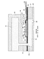
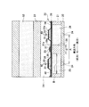
(インクジェットヘッドの詳細)
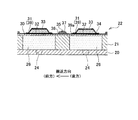
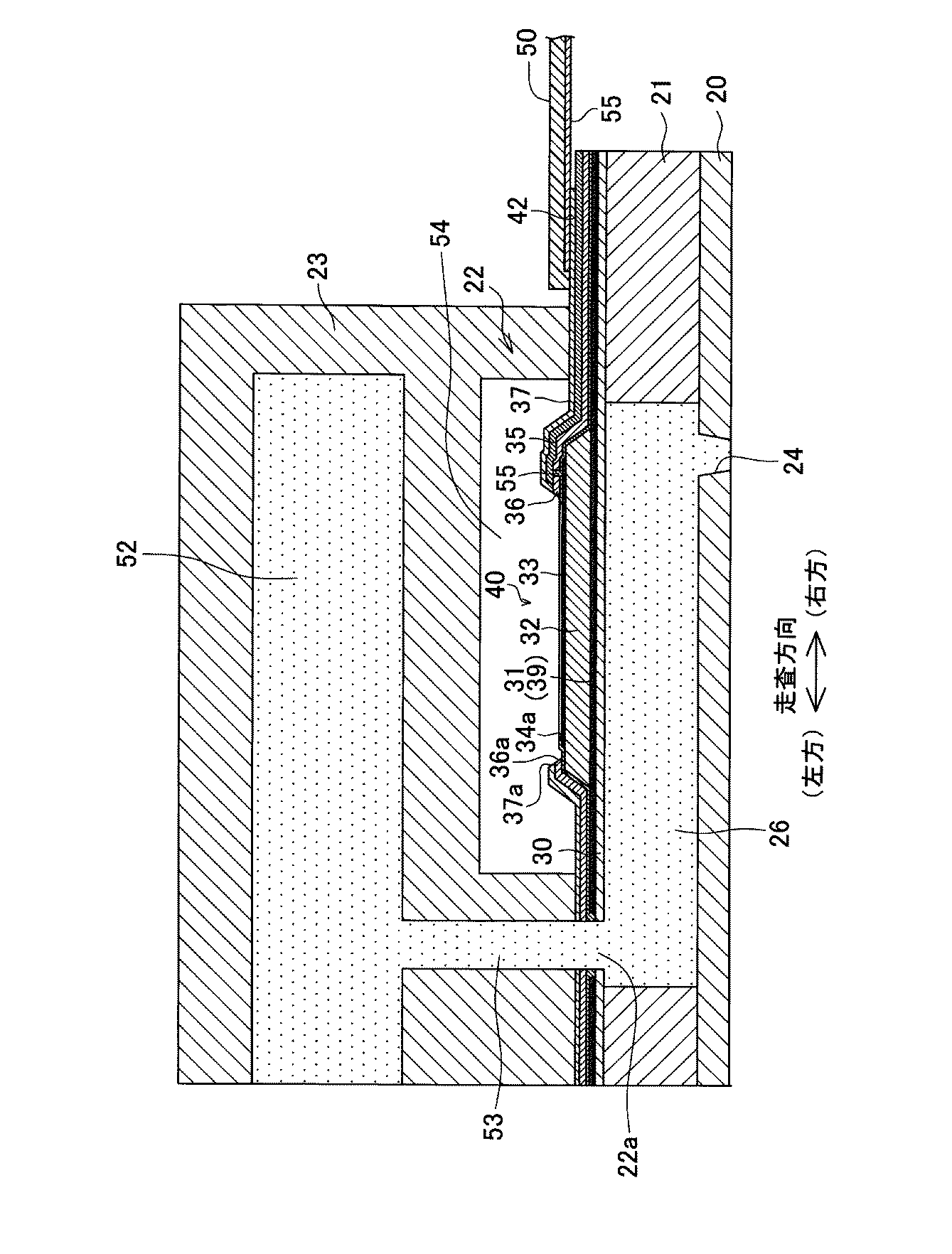
次に、インクジェットヘッド4の詳細構成について説明する。図2は、インクジェットヘッド4の1つのヘッドユニット16の上面図である。尚、インクジェットヘッド4の4つのヘッドユニット16は、全て同じ構成であるため、そのうちの1つについて説明を行い、他のヘッドユニット16については説明を省略する。図3は、図2のA部拡大図である。図4は、図3のIV-IV線断面図である。図5は、図3のV-V線断面図である。
(Details of inkjet head)
Next, the detailed configuration of the
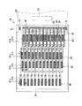
図2〜図5に示すように、ヘッドユニット16は、ノズルプレート20、流路基板21、圧電アクチュエータ22、及び、リザーバ形成部材23を備えている。尚、図2では、図面の簡素化のため、流路基板21及び圧電アクチュエータ22の上方に位置する、リザーバ形成部材23は、二点鎖線で外形のみ示されている。
As shown in FIGS. 2 to 5, the
(ノズルプレート)
ノズルプレート20は、ステンレス鋼等の金属材料、シリコン、あるいは、ポリイミド等の合成樹脂材料などで形成されている。ノズルプレート20には、複数のノズル24が形成されている。図2に示すように、1色のインクを吐出する複数のノズル24は、搬送方向に配列されて、左右方向に並ぶ2つのノズル列25a,25bを構成している。2列のノズル列25a,25bの間では、搬送方向におけるノズル24の位置が、各ノズル列25の配列ピッチPの半分(P/2)だけずれている。
(Nozzle plate)
The
(流路基板)
流路基板21は、シリコンで形成された基板である。この流路基板21の下面に、前述したノズルプレート20が接合されている。流路基板21には、複数のノズル24とそれぞれ連通する複数の圧力室26が形成されている。各圧力室26は、走査方向に長い矩形の平面形状を有する。複数の圧力室26は、前述した複数のノズル24の配列に応じて搬送方向に配列され、左右方向に並ぶ2つの圧力室列27(27a,27b)を構成している。
(Channel substrate)
The
(圧電アクチュエータ)
圧電アクチュエータ22は、複数の圧力室26内のインクに、それぞれノズル24から吐出させるための吐出エネルギーを付与するものである。圧電アクチュエータ22は、流路基板21の上面に配置されている。
(Piezoelectric actuator)
The
図2〜図5に示すように、圧電アクチュエータ22は、振動膜30、複数の圧電素子40、保護膜34、層間絶縁膜36、配線35、及び、配線保護膜37を有する。尚、図2では、図面の簡単のため、図3〜図5には示されている、圧電膜32を覆う保護膜34や、配線35を覆う配線保護膜37の図示は省略されている。
As shown in FIGS. 2 to 5, the
図2、図3に示すように、圧電アクチュエータ22の、複数の圧力室26の端部とそれぞれ重なる位置に、複数の連通孔22aが形成されている。これら複数の連通孔22aにより、後述するリザーバ形成部材23内の流路と、複数の圧力室26とがそれぞれ連通している。
As shown in FIGS. 2 and 3, a plurality of communication holes 22 a are formed at positions where the
振動膜30は、流路基板21の上面の全域に、複数の圧力室26を覆うように配置されている。振動膜30は、二酸化シリコン(SiO2)、あるいは、窒化シリコン(SiNx)等で形成されている。振動膜30の厚みは、例えば、1μm程度である。
The
複数の圧電素子40は、振動膜30を挟んで、複数の圧力室26とそれぞれ対向して配置されている。即ち、複数の圧電素子40は、圧力室26の配列に応じて搬送方向に配列され、且つ、走査方向に並ぶ2つの圧電素子列41を構成している。各圧電素子40は、下部電極31、圧電膜32、及び、上部電極33を有する。
The plurality of
下部電極31は、振動膜30の上面の、圧力室26と対向する領域に形成されている。また、図5に示すように、複数の圧力室26の間の領域には下部電極31と同じ材料によって導電膜38が形成され、この導電膜38により、複数の圧電素子40の間で下部電極31同士が導通している。言い換えれば、振動膜30の上面のほぼ全域に、複数の下部電極31とそれらの間の導電膜38からなる、1つの大きな共通電極39が配置されている。下部電極31の材質は特に限定されないが、例えば、白金(Pt)とチタン(Ti)の2層構造のものを採用することができる。この場合、白金層は200nm、チタン層は50nm程度とすることができる。
The
圧電膜32は、振動膜30の圧力室26と対向する領域において、下部電極31の上に形成されている。図3に示すように、圧電膜32は、圧力室26よりも小さい、走査方向に長い矩形の平面形状を有する。圧電膜32は、例えば、チタン酸鉛とジルコン酸鉛との混晶であるチタン酸ジルコン酸鉛(PZT)を主成分とする圧電材料からなる。圧電膜32の厚みは、例えば、1μm〜5μm程度である。
The
上部電極33は、圧電膜32よりも一回り小さい、矩形の平面形状を有する。上部電極33は、圧電膜32の上面の中央部に形成されている。上部電極33は、例えば、イリジウム(Ir)などで形成されている。上部電極33の厚みは、例えば、80nm程度である。
The
図3〜図5に示すように、保護膜34は、複数の圧電素子40の圧電膜32に跨って、振動膜30の上面のほぼ全域にわたって形成されている。保護膜34は、空気中に含まれる水分の、圧電膜32への侵入を防止するための膜であり、この保護膜34は、アルミナ(Al2O3)などの耐水性を有する材料で形成されている。この保護膜34の厚みは、例えば、80nm程度である。空気中の水分が圧電膜32内に入り込むと圧電膜32が劣化するが、圧電膜32が保護膜34によって覆われていることで、圧電膜32への水分の侵入が防止される。
As shown in FIGS. 3 to 5, the
また、保護膜34による圧電膜32の変形阻害を小さくするために、保護膜34の、その厚み方向から見て圧電膜32の上面の中央部と重なる部分に、矩形状の開口部34aが形成されている。これにより、上部電極33の大部分が保護膜34から露出している。尚、開口部34aの内側領域においては、圧電膜32は保護膜34によって覆われていないものの、上部電極33によって覆われているため、外部からの圧電膜32への水分の侵入が抑制される。
Further, in order to reduce deformation inhibition of the
図3〜図5に示すように、層間絶縁膜36は、保護膜34の上に形成されている。層間絶縁膜36には、保護膜34の開口部34aよりも一回り大きい開口部36aが形成されている。これにより、層間絶縁膜36は、圧力室26を隔てる隔壁28を覆うように配置され、圧電素子40の大部分は層間絶縁膜36から露出している。尚、圧電素子40の周囲における層間絶縁膜36の形成範囲の詳細について、配線保護膜37の形成範囲とともに詳しく述べる。
As shown in FIGS. 3 to 5, the
層間絶縁膜36の上には、次述の複数の配線35が配置される。層間絶縁膜36は、主に、複数の配線35と共通電極39の導電膜38との間の絶縁性を高めるために設けられている。層間絶縁膜36の材質は特に限定されないが、例えば、二酸化シリコン(SiO2)で形成される。また、共通電極39と配線35間の絶縁性確保の観点から、層間絶縁膜36の膜厚は、ある程度厚いことが好ましく、例えば、300〜500nmである。
On the
配線は、圧電素子40に電圧を印加するためのものであり、層間絶縁膜36の上に配置されている。配線35の一端部は、圧電膜32の右端部の上面に、保護膜34及び層間絶縁膜36を介して被さるように配置されている。また、保護膜34と層間絶縁膜36の、上部電極33の右端部を覆う部分には、これらの膜を貫通するように配置された導通部55が設けられている。そして、導通部55を介して配線35と上部電極33の右端部とが導通している。また、複数の圧電素子40に対応する複数の配線35は、上部電極33からそれぞれ右方へ引き出されている。配線35は、例えば、アルミニウム(Al)で形成されている。
The wiring is for applying a voltage to the
尚、左右2つの圧電素子列41のうち、左側の圧電素子列41aから引き出された配線35は、右側の圧電素子列41bの圧電素子40間において、層間絶縁膜36の上に配置されている。即ち、左側の圧電素子40に接続された配線35は、隔壁28の上方において、右側の2つの圧電素子40の間を通過して右方へ延びている。尚、各配線35の厚みは、断線等を極力防止するために、一定以上の厚みであることが好ましく、例えば、1μm程度である。
Of the two left and right
配線35の下の層間絶縁膜36は、流路基板21の右端部まで形成されている。図2に示すように、流路基板21の右端部においては、層間絶縁膜36の上に、複数の駆動接点42が搬送方向に並べて配置されている。上部電極33から右方へ引き出された配線35は駆動接点42と接続されている。また、流路基板21の右端部には、複数の駆動接点42の搬送方向両側に、2つのグランド接点43も配置されている。グランド接点43は、保護膜34及び層間絶縁膜36を貫通する導通部(図示省略)を介して、保護膜34の下側に配置されている共通電極39と接続されている。
The
配線保護膜37は、層間絶縁膜36の上に、複数の配線35を覆うように形成されている。この配線保護膜37は、主に、配線35の保護、及び、配線35間の絶縁確保の目的で設けられている。配線保護膜37は、例えば、窒化シリコン(SiNx)等で形成されている。配線保護膜37の厚みは、例えば、100nm〜1μmである。
The wiring
図3〜図5に示すように、層間絶縁膜36と同様、配線保護膜37にも開口部37aが形成されている。配線保護膜37の開口部37aは、層間絶縁膜36の開口部36aとほぼ同じ大きさである。これにより、配線保護膜37は、圧力室26を隔てる隔壁28上において、配線35を覆うように配置される一方、配線35の両側に位置する圧電素子40の大部分は配線保護膜37から露出している。また、配線保護膜37の開口部37aは、保護膜34の開口部34aよりも一回り大きい。
As shown in FIGS. 3 to 5, similarly to the
図3、図4に示すように、配線保護膜37は、流路基板21の右端部まで延び、配線35の駆動接点42との接続箇所までの部分を覆っている。一方、複数の駆動接点42とグランド接点43は、配線保護膜37からは露出しており、流路基板21の右端部上面に接合される後述のCOF50と電気的に接続される。
As shown in FIGS. 3 and 4, the wiring
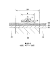
圧電素子40の周囲における、層間絶縁膜36と配線保護膜37の形成範囲について、詳細に説明する。図6は、図5の隔壁周辺の拡大図である。
The formation range of the
まず、搬送方向、即ち、圧力室26の短手方向における膜36,37の形成範囲について説明する。図3、図5、図6に示すように、搬送方向に隣接する2つの圧電素子40の間において、層間絶縁膜36が隔壁28の上に配置されている。また、層間絶縁膜36の上の配線35を覆うように配線保護膜37が配置されている。
First, the formation range of the
また、2つの圧電素子40の間において、配線保護膜37及び層間絶縁膜36の搬送方向における両端は、隔壁28の端よりも内側にある。即ち、隔壁28の上の配線保護膜37及び層間絶縁膜36は、隔壁28で隔てられた圧力室26と対向する領域まではみ出していない。この構成では、圧力室26の上に、層間絶縁膜36及び配線保護膜37の端が位置しない。従って、圧電素子40の駆動時に、配線保護膜37及び層間絶縁膜36の端を起点として、圧力室26を覆う振動膜30にクラックが生じることが抑制される。尚、図6に示すように、配線保護膜37及び層間絶縁膜36の幅Wは、隔壁28の幅W1に対して、3.8μm以上小さいことが好ましい。その理由については後で述べる。
Further, between the two
後でも説明するが、配線保護膜37と層間絶縁膜36のエッチングを同じ工程で行うことから、配線保護膜37の開口部37aと層間絶縁膜36の開口部36aの位置が一致する。これにより、隔壁28の上における、配線保護膜37の端と層間絶縁膜36の端は、搬送方向において同じ位置にある。尚、エッチングの際に形成される膜端のテーパ形状によって、実際には、配線保護膜37の端位置と層間絶縁膜36の端位置はわずかにずれるが、上述した「配線保護膜37の端と層間絶縁膜36の端が同じ位置にある」構成には、この僅かなずれが存在する場合も含むものとする。
As will be described later, since the etching of the wiring
次に、走査方向、即ち、圧力室26の長手方向における膜36,37の形成範囲について、図4を参照して説明する。振動膜30の、圧電膜32の長手方向端部と重なる位置においては、圧電素子40の変形時に応力が集中しやすい。この応力集中を抑えるため、層間絶縁膜36と配線保護膜37が上記の位置まで形成されている。即ち、図3、図4に示すように、層間絶縁膜36とその上の配線保護膜37は、圧力室26の長手方向両端部と重なって配置されている。これにより、圧電膜32の端部が、層間絶縁膜36と配線保護膜37に覆われてこの位置での剛性が高まる。この場合、長手方向の端部近傍での屈曲が穏やかになるため、振動膜30のクラックが抑制される。
Next, the formation range of the
尚、配線保護膜37及び層間絶縁膜36が、長手方向において圧力室26と一部重なり、且つ、圧電膜32には乗りあげていない構成だと、圧力室26の短手方向に膜36,37が圧力室26まではみ出した場合と同様、膜36,37の端を起点とするクラックが振動膜30に発生しやすくなる。この点、配線保護膜37と層間絶縁膜36の端が、圧電膜32の上面まで乗りあげていることにより、膜36,37の端を起点とするクラックも抑制される。
If the wiring
また、層間絶縁膜36と配線保護膜37が、圧力室26や圧電膜32と一部重なっていると、圧電素子40の駆動時における振動膜30の変位が阻害されるという問題がある。しかし、変位に大きな影響を与えるのは圧力室26の短手方向における膜構成であり、これに比べると長手方向の端部の構成については変位へ与える影響は小さい。そこで、本実施形態では、多少、変位低下の問題があるものの、振動膜30のクラック発生をより確実に防止するために、圧力室26の長手方向においては、配線保護膜37と層間絶縁膜36が、圧力室26や圧電膜32と部分的に重なった構成が採用されている。
Further, when the
図2〜図4に示すように、圧電アクチュエータ22の右端部の上面には、配線部材であるCOF(Chip On Film)50がそれぞれ接合されている。そして、COF50に形成された複数の配線55が、複数の駆動接点42と、それぞれ電気的に接続されている。COF50の、駆動接点42と反対側の端部は、プリンタ1の制御装置6(図1参照)に接続されている。また、COF50にはドライバIC51が実装されている。
As shown in FIGS. 2 to 4, a COF (Chip On Film) 50, which is a wiring member, is joined to the upper surface of the right end portion of the
ドライバIC51は、制御装置6から送られてきた制御信号に基づいて、圧電アクチュエータ22を駆動するための駆動信号を生成して出力する。ドライバIC51から出力された駆動信号は、COF50の配線55を介して駆動接点42に入力され、さらに、圧電アクチュエータ22の配線35を介して上部電極33に供給される。駆動信号が供給された上部電極33の電位は、所定の駆動電位とグランド電位との間で変化する。また、COF50には、グランド配線(図示省略)も形成されており、このグランド配線は、圧電アクチュエータ22のグランド接点43と電気的に接続される。これにより、グランド接点43と接続されている共通電極39の電位は、常にグランド電位に維持される。
The
ドライバIC51から駆動信号が供給されたときの、圧電アクチュエータ22の動作について説明する。駆動信号が供給されていない状態では、上部電極33の電位はグランド電位であり、共通電極39と同電位である。この状態から、ある上部電極33に駆動信号が供給されて駆動電位が印加されると、その上部電極33と共通電極39との電位差により、圧電膜32に、その厚み方向に平行な電界が作用する。このとき、圧電逆効果によって、圧電膜32は厚み方向に伸びて面方向に収縮する。さらに、この圧電膜32の収縮変形に伴って、振動膜30が圧力室26側に凸となるように撓む。これにより、圧力室26の容積が減少して圧力室26内に圧力波が発生することで、圧力室26に連通するノズル24からインクの液滴が吐出される。
The operation of the
(リザーバ形成部材)
図4、図5に示すように、リザーバ形成部材23は、圧電アクチュエータ22を挟んで、流路基板21と反対側(上側)に配置され、圧電アクチュエータ22の上面に接着剤で接合されている。リザーバ形成部材23は、例えば、流路基板21と同様、シリコンで形成されてもよいが、シリコン以外の材料、例えば、金属材料や合成樹脂材料で形成されていてもよい。
(Reservoir forming member)
As shown in FIGS. 4 and 5, the
リザーバ形成部材23の上半部には、搬送方向に延びるリザーバ52が形成されている。このリザーバ52は、インクカートリッジ17が装着されるカートリッジホルダ7(図1参照)と、図示しないチューブでそれぞれ接続されている。
A
図4に示すように、リザーバ形成部材23の下半部には、リザーバ52から下方に延びる複数のインク供給流路53が形成されている。各インク供給流路53は、圧電アクチュエータ22の複数の連通孔22aに連通している。これにより、リザーバ52から、複数のインク供給流路53、及び、複数の連通孔22aを介して、流路基板21の複数の圧力室26にインクが供給される。また、リザーバ形成部材23の下半部には、圧電アクチュエータ22の複数の圧電素子40を覆う、凹状の保護カバー部54も形成されている。
As shown in FIG. 4, a plurality of
次に、上述したインクジェットヘッド4のヘッドユニット16の製造工程について、特に、圧電アクチュエータ22の製造工程を中心に、図7〜図12を参照して説明する。
Next, the manufacturing process of the
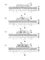
図7は、(a)振動膜成膜、(b)共通電極成膜、(c)圧電材料膜成膜、(d)上部電極用の導電膜成膜、(e)導電膜エッチング(上部電極形成)の、各工程を示す図である。 FIG. 7 shows (a) vibration film formation, (b) common electrode film formation, (c) piezoelectric material film formation, (d) upper electrode conductive film formation, (e) conductive film etching (upper electrode) It is a figure which shows each process of formation.
まず、図7(a)に示すように、シリコン基板である流路基板21の表面に、二酸化シリコンの振動膜30を成膜する。振動膜30の成膜法としては、熱酸化処理を好適に採用できる。次に、図7(b)に示すように、振動膜30の上に、複数の下部電極31となる共通電極39をスパッタリング等により成膜する。また、図7(c)に示すように、共通電極39の上に、ゾルゲルやスパッタリング等で、共通電極39の上面全域にPZTなどの圧電材料からなる圧電材料膜59を成膜する。
First, as shown in FIG. 7A, a silicon
さらに、圧電材料膜59の上面に上部電極33を形成する。まず、図7(d)に示すように、スパッタリング等で、圧電材料膜59の上面に導電膜57を成膜する。次に、この導電膜57にエッチングを施すことにより、圧電材料膜59の上面に、複数の上部電極33をそれぞれ形成する。
Further, the
図8は、(a)圧電材料膜エッチング(圧電素子形成)、(b)共通電極エッチング、(c)保護膜成膜、(d)層間絶縁膜成膜、(e)上部電極と配線の導通用の孔形成の、各工程を示す図である。 FIG. 8 shows (a) piezoelectric material film etching (piezoelectric element formation), (b) common electrode etching, (c) protective film formation, (d) interlayer insulation film formation, (e) upper electrode and wiring conduction. It is a figure which shows each process of common hole formation.
図8(a)に示すように、圧電材料膜59のエッチングを行って複数の圧電膜32を形成する。これにより、振動膜30の上に、複数の圧電素子40が形成される。また、図8(b)に示すように、共通電極39にエッチングを行って、圧電アクチュエータ22の連通孔22a(図4参照)の一部を構成する、孔31aを形成する。
As shown in FIG. 8A, the
次に、図8(c)に示すように、複数の圧電素子40を覆うように、保護膜34をスパッタリング等で成膜する。さらに、図8(d)に示すように、保護膜34の上に層間絶縁膜36を成膜する。層間絶縁膜36は、複数の圧電素子40を覆い、さらに、複数の圧電素子40の間の隔壁28をも覆うように形成する。尚、二酸化シリコンからなる層間絶縁膜36は、プラズマCVDによって好適に成膜することができる。
Next, as shown in FIG. 8C, a
保護膜34と層間絶縁膜36を成膜したら、図8(e)に示すように、保護膜34と層間絶縁膜36の、上部電極33の端部を覆う部分に、エッチングで孔56を形成する。この孔56は、上部電極33と、次工程で層間絶縁膜36の上に形成される配線35とを導通するための孔である。
When the
図9は、(a)配線用の導電膜成膜、(b)導電膜エッチング(配線形成)、(c)配線保護膜成膜の、各工程を示す図である。次に、保護膜34の上の層間絶縁膜36に、複数の配線35を形成する。まず、図9(a)に示すように、層間絶縁膜36の上面に、スパッタリング等で導電膜58を成膜する。このとき、導電材料の一部が孔56に充填されることによって、孔56内に、上部電極33と導電膜58とを導通させる導通部55が形成される。次に、図9(b)に示すように、この導電膜58にエッチングを施して不要な部分を除去し、複数の配線35をそれぞれ形成する。
FIG. 9 is a diagram showing each step of (a) forming a conductive film for wiring, (b) etching a conductive film (wiring formation), and (c) forming a wiring protective film. Next, a plurality of
次に、図9(c)に示すように、複数の圧電素子40、及び、これら複数の圧電素子40にそれぞれ接続された複数の配線35を覆うように配線保護膜37を成膜する。窒化シリコン(SiNx)からなる配線保護膜37は、先の層間絶縁膜36と同様、プラズマCVDで成膜するのが好ましい。
Next, as shown in FIG. 9C, a wiring
図10は、(a)層間絶縁膜及び配線保護膜の一部除去、(b)保護膜の一部除去、(c)振動膜の孔形成、の各工程を示す図である。 FIG. 10 is a diagram showing each step of (a) partial removal of the interlayer insulating film and wiring protective film, (b) partial removal of the protective film, and (c) formation of holes in the vibration film.
次に、図10(a)に示すように、配線保護膜37と層間絶縁膜36にエッチングを行って、配線保護膜37及び層間絶縁膜36の、複数の圧電素子40を覆っている部分を同時に除去する。これにより、配線保護膜37に開口部37aを形成するとともに、層間絶縁膜36に開口部36aを形成して、それらの下にある保護膜34を露出させる。
Next, as shown in FIG. 10A, the wiring
配線保護膜37と層間絶縁膜36の除去は、具体的には次のようにして行う。まず、配線保護膜37の表面に、フォトレジストにより、開口部36a,37aの形成領域以外を覆うマスクを形成する。マスクを形成したら、配線保護膜37の表面からのエッチングを行って、配線保護膜37と層間絶縁膜36を同時に除去し、2種類の膜37,36の、マスクによって覆われていない領域に開口部36a,37aを形成する。エッチング後、マスクを剥離して除去する。
Specifically, the wiring
図11は、層間絶縁膜36と配線保護膜37の除去工程を説明する図である。図11に示すように、搬送方向に並ぶ2つの圧力室26を隔てる隔壁28においては、配線35の下側の層間絶縁膜36と、配線35を上から覆う配線保護膜37が、除去されずに残される。その際に、層間絶縁膜36と配線保護膜37の端が、隔壁28の端よりも外側へはみ出さないようする。
FIG. 11 is a diagram for explaining a process of removing the
具体的には、層間絶縁膜36と配線保護膜37の搬送方向における端の目標形成位置P0を、隔壁28の端の目標形成位置P1よりも内側に設定して除去工程を行う。ここで、「膜36,37の端の目標形成位置」とは、膜36,37をエッチングする際の端の目標位置であり、膜36,37の端がその位置にくるように、マスク位置やエッチング量等を調整する。同様に、「隔壁28の端の目標形成位置」とは、後述する圧力室26の形成工程(図12(b))において、流路基板21をエッチングして圧力室26を形成する際の端の目標位置であり、隔壁28の端がその位置にくるように、マスクやエッチング量等を調整する。別の言い方をすれば、上記の「目標形成位置」は、ヘッドユニットを製造する際の設計図面に明記されている位置(寸法)のことである。
Specifically, the removal process is performed by setting the target formation position P0 at the end in the transport direction of the
但し、膜36,37のエッチングの際に生じる様々なズレによって、図11に二点鎖線で示すように、膜36,37の端は目標形成位置P0からずれうる。また、隔壁28の端についても同様に、エッチングによる圧力室26の形成時に生じるズレによって、目標形成位置P1からずれうる。その結果、加工後の膜36,37の端の位置が、隔壁28の端よりも内側に来ない場合も想定される。
However, the ends of the
本願発明者らは、当初、膜36,37の端が隔壁28の端に一致するように、端位置の目標を設定してヘッドユニットを製造して駆動試験を行ったのであるが、その試験において、振動膜30にクラックが発生した。調査の結果、エッチングの際のズレによって、膜36,37の端が隔壁28の端よりも外側にはみ出し、膜36,37の一部が圧力室26と重なっていることがわかった。尚、この試作品における振動膜30の厚みは、1.0μm〜1.4μmであった。
The inventors of the present application manufactured a head unit by setting a target of the end position so that the ends of the
そこで、膜36,37の目標形成位置P0は、隔壁28の端の目標形成位置P1よりも、3μm以上内側の位置であることが好ましい。その理由は、以下の通りである。
Therefore, it is preferable that the target formation position P0 of the
層間絶縁膜36及び配線保護膜37の除去工程では、マスクのズレに起因して隔壁28上での膜の位置(a)がばらつき、また、エッチングの加工ズレによって膜幅(b)がばらつく。これにより、膜36,37の端の位置がずれうる。また、圧力室26の形成工程(図12(b))において、マスクのズレに起因して隔壁28の位置(c)がばらつき、また、エッチングの加工ズレによって隔壁28の幅(d)がばらつく。これにより、隔壁28の端の位置もずれうる。そのため、膜36,37の端位置と隔壁28の端位置の間の離間距離Tが、ある範囲内でばらつくことになる。そこで、上記の様々なズレが生じたとしても、膜36,37の実際の端位置が隔壁28の端位置P1よりも内側となるように、膜36,37の端の目標形成位置P0を設定するのがよい。
In the step of removing the
上記の各種ズレの程度は、膜36,37のエッチングや圧力室26の形成に使用する装置の精度に依存するものの、おおよそ、表1に示すような値となる。また、表1の値は、3σでの値を示し、ズレがこの範囲内に入る確率は99.7%である。表1において、「マスクズレ」とは、エッチング用マスクが面方向と平行にずれることによる、位置ズレの程度を示す。また、「加工ズレ」とは、エッチングの加工幅のずれの程度を示す。例えば、「圧力室形成時のマスクズレが±3μm」とは、流路基板21にエッチングで圧力室26を形成する際に、エッチングマスクが、目標の設置位置に対して最大3μmずれるということである。
The degree of the various misalignments described above is a value as shown in Table 1, although it depends on the accuracy of the apparatus used for etching the
尚、上述したように、層間絶縁膜36と配線保護膜37の除去を同時に行うことで、除去工程の回数が減る。このことは、マスクズレや加工ズレの発生機会が減ることを意味する。これに対して、2種類の膜36,37の除去を別々に行った場合には、2回の除去工程のそれぞれでマスクズレや加工ズレが発生することから、ズレ量が大きくなりうる。
As described above, the removal of the
表1のズレの程度から、目標形成位置P0をどのように設定するのが適切かについて、以下、検討を行う。
(1)1つの考え方として、表1のズレの種類の中でも最大の、圧力室形成時のマスクズレ(最大3μm)に着目する。即ち、このマスクズレが生じても、膜36,37の端位置が隔壁28からはみ出ないように、目標形成位置P0を設定するということである。この考え方に従えば、膜36,37の端の目標形成位置P0は、隔壁28の端の目標形成位置P1よりも、3μm以上内側に設定すればよい。
Based on the degree of deviation in Table 1, how to set the target formation position P0 is considered below.
(1) As one way of thinking, attention is focused on the largest mask displacement (maximum of 3 μm) at the time of forming the pressure chamber among the types of displacement in Table 1. That is, the target formation position P0 is set so that the end positions of the
(2)もう1つの考え方として、表1の全ての種類のズレがそれぞれ生じた場合でも、膜36,37の端位置が隔壁28からはみ出ないように、目標形成位置P0を設定してもよい。尚、この場合に、全種類のズレの最大値の合計、つまり、個々の最悪値を積み上げた値を基に、目標形成位置P0を設定することも可能である。しかし、全種類のズレが、全て最大のズレ量となる確率は0に限りなく近く、そのような条件もカバーするように設計することは現実的ではない。
(2) As another idea, the target formation position P0 may be set so that the end positions of the
そこで、「二乗和公差」という考え方に基づいて、目標形成位置P0を決定することが好ましい。前提として、表1の4種類の寸法(a〜d)は、各々が他の寸法に影響を及ぼさない。即ち、a〜dは独立の事象である。この場合に、距離Tのばらつきが正規分布に従うとすると、分散の加法性から、距離Tの分散T2は、下記式で表される。 Therefore, it is preferable to determine the target formation position P0 based on the concept of “square sum tolerance”. As a premise, each of the four types of dimensions (ad) in Table 1 does not affect other dimensions. That is, a to d are independent events. In this case, assuming that the variation in the distance T follows a normal distribution, the dispersion T 2 of the distance T is expressed by the following equation from the additivity of the dispersion.
尚、表1における加工ズレ(b,d)は、膜幅又は隔壁の幅という、幅寸法のズレの値であることから、端位置のズレ量を求める際には、数1に示すように、幅寸法のズレについてはその半分の値を使用している。上の式を変形して、標準偏差の形にすると、下記式となる。 Since the processing deviation (b, d) in Table 1 is the value of the deviation of the width dimension, that is, the film width or the partition wall width, when obtaining the deviation amount of the end position, as shown in Equation 1. The half value is used for the deviation of the width dimension. If the above equation is modified to form a standard deviation, the following equation is obtained.
a〜dに、表1のズレの値を代入すると、T=3.17となる。上記a〜dの値は、それぞれ3σでの値であるから、Tについても、99.7%の確率で3.17μm以下となる。実際上は、膜36,37の端位置の目標形成位置P0を、隔壁28の端位置P1よりも3μm以上内側の位置に設定しておけば、膜36,37が、隔壁28の端よりも外側にはみ出すことはまずないと言える。
Substituting the deviation values in Table 1 for a to d results in T = 3.17. Since the values a to d are values at 3σ, T is 3.17 μm or less with a probability of 99.7%. Actually, if the target formation position P0 of the end positions of the
尚、隔壁28の上の膜36,37の端の目標形成位置P0については、隔壁28の寸法との関係で表現することも可能である。ノズル24及び圧力室26が、300dpiの配列である場合、圧力室26の配列ピッチは84.7μm(図5の寸法A)となる。一方で、各々のノズル24から正常にインクを吐出するためには、圧力室26の幅を60〜70μm(図5の寸法B)とすることが好ましい。双方の条件を考慮すれば、2つの圧力室26を隔てる隔壁28が取り得る幅(図5の寸法C)は、14.7μm〜24.7μmとなる。このときに、膜36,37の端の目標形成位置P0を、隔壁28の目標形成位置P1からの距離が3μmの位置に設定するということは、P0とP1の距離が、隔壁28の幅の12%(3μm/24.7μm)〜20%(3μm/12.7μm)となるように設定することと同義である。即ち、P0とP1の距離を3μm以上にするには、上記距離が、隔壁28の幅の12%以上となるように設定すればよい。
The target formation position P0 at the ends of the
尚、上記のようにして膜36,37の除去工程を行った後の、膜36,37の幅と隔壁28の幅との関係は、次のようになる。膜36,37の端の目標形成位置P0を、隔壁28の端から3μm離れた位置に設定したときに、理論上は、図6の膜36,37の幅Wは、隔壁28の幅W1と比べて、左右両側で3μmずつ、合計で6μm小さくなる。但し、実際には、表1に示される膜36,37の加工ズレによる膜幅のばらつき、及び、圧力室26の加工ズレによる隔壁28の幅のばらつきを考慮する必要がある。これらの加工ズレを加味すると、実際に形成される膜36,37の幅Wと隔壁28の幅W1の関係は、以下のようになる。
W≦W1−(3μm×2)+(0.2μm)+(2μm)=W1−3.8μm
The relationship between the widths of the
W ≦ W1− (3 μm × 2) + (0.2 μm) + (2 μm) = W1−3.8 μm
図10に戻り、上述の配線保護膜37と層間絶縁膜36の除去工程が終わったら、次に、図10(b)に示すように、配線保護膜37及び層間絶縁膜36から露出した保護膜34にエッチングを行い、保護膜34に開口部34aを形成する。さらに、図10(c)に示すように、振動膜30にエッチングを施し、圧電アクチュエータ22の連通孔22a(図4参照)の一部を構成する、孔30aを形成する。図10(c)の工程で、圧電アクチュエータ22の製造が完了する。
Returning to FIG. 10, after the above-described removal process of the wiring
図12は、(a)流路基板の研磨、(b)流路基板のエッチング(圧力室形成)、(c)ノズルプレートの接合、(d)リザーバ形成部材の接合の、各工程を示す図である。図12(a)に示すように、インク流路が形成される流路基板21を、下面側(振動膜30と反対側)から研磨によって除去し、流路基板21の厚みを、所定の厚みまで薄くする。流路基板21の元となるシリコンウェハーの厚みは、500μm〜700μm程度であるが、この研磨工程で、流路基板21の厚みを100μm程度まで薄くする。
12A and 12B are diagrams showing respective steps of (a) polishing the flow path substrate, (b) etching the flow path substrate (forming the pressure chamber), (c) bonding the nozzle plate, and (d) bonding the reservoir forming member. It is. As shown in FIG. 12A, the
上記の研磨後、図12(b)に示すように、流路基板21の、振動膜30と反対側の下面側からエッチングを行って、圧力室26を形成する。尚、この流路基板21のエッチングは、ウェットエッチングでもドライエッチングでもよい。但し、一般に、ドライエッチングでは、化学的な反応だけでなく物理的な作用によるエッチングも生じるため、振動膜30の厚みが、目標とする寸法よりも薄くなることもあり得る。そのため、特に、ドライエッチングで圧力室26を形成する場合に本発明を適用することは効果的である。さらに、図12(c)に示すように、流路基板21の下面に、ノズルプレート20を接着剤で接合する。最後に、図12(d)に示すように、圧電アクチュエータ22に、リザーバ形成部材23を接着剤で接合する。
After the above polishing, as shown in FIG. 12B, the
以上説明した実施形態において、搬送方向、及び、圧力室26の短手方向が、本発明の「第1方向」に相当し、走査方向、及び、圧力室26の長手方向が、本発明の「第2方向」に相当する。右側の圧力室列27bの2つの圧力室26が、本発明の「第1圧力室」と「第2圧力室」に相当する。振動膜30が、本発明の「第1絶縁膜」に相当する。右側の圧電素子列41bの2つの圧電素子40が、本発明の「第1圧電素子」と「第2圧電素子」に相当する。配線保護膜37が、本発明の「第2絶縁膜」に相当する。層間絶縁膜36が、本発明の「第3保護膜」に相当する。
In the embodiment described above, the transport direction and the short direction of the
また、図9(c)の配線保護膜37を成膜する工程が、本発明の「第1の絶縁膜形成工程」に相当する。図8(d)の層間絶縁膜36を成膜する工程が、本発明の「第2の絶縁膜形成工程」に相当する。図10(a)の、配線保護膜37と層間絶縁膜36の除去工程が、本発明の「第1の除去工程」に相当する。
Further, the step of forming the wiring
次に、前記実施形態に種々の変更を加えた変更形態について説明する。但し、前記実施形態と同様の構成を有するものについては、同じ符号を付して適宜その説明を省略する。 Next, modified embodiments in which various modifications are made to the embodiment will be described. However, components having the same configuration as in the above embodiment are given the same reference numerals and description thereof is omitted as appropriate.
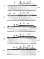
1]前記実施形態では、下部電極31と導電膜38からなる共通電極39が、振動膜30の上面のほぼ全域に形成された構成であり、隔壁28の上には導電膜38が配置されている(図5参照)。この構成では、圧電素子40の焼成の際の共通電極39の収縮に起因して、圧電素子40や流路基板21には、流路基板21の面方向に大きな引張応力が残る。そして、この引張応力は、圧電素子40の変形を阻害する1つの要因となる。そこで、図13〜図15に示すように、共通電極39がパターニングされて、搬送方向に並ぶ圧電素子40の間において、共通電極39に開口部39aが形成されていてもよい。これにより、共通電極39が面全体で大きく収縮することが抑えられ、上記の引張応力は小さくなる。
1] In the above-described embodiment, the
ただし、共通電極39の開口部39aの位置においては、振動膜30の表面に、延性・展性のある金属膜が存在しないことになり、クラックに対して弱くなるという問題がある。そのため、特に上記の場合に、振動膜30のクラック発生を抑えるために、層間絶縁膜36と配線保護膜37の端が、隔壁28の端よりも内側にある構成が採用されることが好ましい。
However, at the position of the
2]前記実施形態では、複数の圧力室26が2つの圧力室列27を構成し、この圧力室の配列に応じて、複数の圧電素子40の配列も2列となっているが、圧力室26や圧電素子40の列数は、2列には限られない。
2] In the above-described embodiment, the plurality of
例えば、図16に示すように、圧力室26及び圧電素子40の列数が4列であってもよい。4つの圧電素子列41(41a〜41b)を構成する圧電素子40の各々に配線35が接続され、全ての配線35が右方へ引き出されている。この構成では、4つの圧電素子列41の間で、圧電素子40の間を通過する配線35の数が異なっている。
For example, as shown in FIG. 16, the number of columns of the
図17は、図16の断面図であり、(a)はA−A線断面図、(b)はB−B線断面図、(c)はC−C線断面図、(d)はD−D線断面図である。図17(a)〜(d)に示すように、4つの圧電素子列41のそれぞれにおいて、搬送方向に隣接する圧電素子40の間には、層間絶縁膜36と配線保護膜37とが形成されている。尚、左端に位置する圧電素子列41aにおいては、隣接する圧電素子40の間に配線35が通っていないものの、他の圧電素子列41と同様に、隔壁28の上に配線保護膜37が形成されている。
17 is a cross-sectional view of FIG. 16, wherein (a) is a cross-sectional view taken along line AA, (b) is a cross-sectional view taken along line BB, (c) is a cross-sectional view taken along line CC, and (d) is a cross-sectional view taken along line D. FIG. As shown in FIGS. 17A to 17D, in each of the four
ここで、4つの圧電素子列41の間で、通過する配線35の数が異なっている場合に、配線35の本数に応じて、層間絶縁膜36や配線保護膜37の幅を変えることも考えられる。しかし、4つの圧電素子列41の間で、隔壁28の上の層間絶縁膜36や配線保護膜37の幅が異なっていると、それらの膜36,37と隔壁28の端、即ち、圧力室26の縁までの距離が異なる。これにより、圧電素子40の間で振動膜30の変位に差が生じて、ノズル24の間における吐出特性の不均一につながる。
Here, when the number of
そこで、通過する配線35の本数に関係なく、膜36,37の、配線35を覆う部分の幅を等しくすることが好ましい。即ち、膜36,37の除去工程において、4つの圧電素子列41のそれぞれについての、膜36,37の端の目標形成位置P0を同じ位置に設定する。これにより、4つの圧電素子列41の間で、隔壁28の端から膜36,37までの距離がほぼ同じとなり、吐出特性の均一化が期待できる。
Therefore, it is preferable to make the widths of the portions of the
尚、図16,図17の形態において、1つの圧力室列27に属する2つの圧力室26が、本発明の「第1圧力室」と「第2圧力室」に相当し、別の1つの圧力室列27に属する2つの圧力室26が、本発明の「第3圧力室」と「第4圧力室」に相当する。また、前記1つの圧力室列27に対応する2つの圧電素子40が、本発明の「第1圧電素子」と「第2圧電素子」に相当し、前記別の1つの圧力室列27に対応する2つの圧電素子40が、本発明の「第3圧電素子」と「第4圧電素子」に相当する。
16 and 17, the two
3]前記実施形態では、層間絶縁膜36と配線保護膜37とを、1回のエッチングで同時に除去しているが、層間絶縁膜36と配線保護膜37を、別々の工程で除去してもよい。この場合、配線保護膜37の除去工程が、本発明の「第1の除去工程」に相当し、層間絶縁膜36の除去工程が、本発明の「第2の除去工程」に相当する。
3] In the above embodiment, the
4]前記実施形態では、配線保護膜37によって覆われる配線35が、圧電素子40に駆動電位を印加するための配線であったが、このような配線には限られない。例えば、共通電極に接続されたグランドの配線であってもよい。
4] In the above-described embodiment, the
5]前記実施形態では、複数の圧電素子の間で下部電極が導通して共通電極を構成する一方で、上部電極が圧電素子に対して個別に設けられた個別電極であったが、下部電極が個別電極で、上部電極が共通電極であってもよい。 5] In the above embodiment, the lower electrode is electrically connected between the plurality of piezoelectric elements to form a common electrode, while the upper electrode is an individual electrode provided individually with respect to the piezoelectric element. May be individual electrodes and the upper electrode may be a common electrode.
6]前記実施形態の圧電アクチュエータ22は、層間絶縁膜36と配線保護膜37の2種類の膜を有する構成である。これに対して、層間絶縁膜36と配線保護膜37の一方のみを有する構成であってもよい。
6] The
例えば、先に説明した図15の形態のように、配線35の直下に共通電極39が配置されていない構成であれば、少なくとも隔壁28の上においては、層間絶縁膜36が形成されていなくてもよい。
For example, as in the configuration of FIG. 15 described above, if the
また、配線35がアルミニウムで形成されている場合は、腐食防止等の目的で、配線35を覆う配線保護膜37が設けられることが好ましいのであるが、金などの安定した材料で形成されている場合には、配線保護膜37が省略されてもよい。
Further, when the
以上説明した実施形態は、本発明を、記録用紙にインクを吐出して画像等を印刷するインクジェットヘッドに適用したものであるが、画像等の印刷以外の様々な用途で使用される液体吐出装置においても本発明は適用されうる。例えば、基板に導電性の液体を吐出して、基板表面に導電パターンを形成する液体吐出装置にも、本発明を適用することは可能である。 In the embodiment described above, the present invention is applied to an ink jet head that prints an image or the like by ejecting ink onto a recording sheet. However, the liquid ejecting apparatus is used for various purposes other than printing an image or the like. The present invention can also be applied. For example, the present invention can also be applied to a liquid ejection apparatus that ejects a conductive liquid onto a substrate to form a conductive pattern on the surface of the substrate.
16 ヘッドユニット
21 流路基板
26 圧力室
28 隔壁
30 振動膜
35 配線
36 層間絶縁膜
37 配線保護膜
40 圧電素子
16
Claims (14)
前記第1圧力室と前記第2圧力室を覆う第1絶縁膜と、
前記第1絶縁膜を挟んで前記第1圧力室と対向して配置された第1圧電素子と、
前記第1絶縁膜を挟んで前記第2圧力室と対向して配置された第2圧電素子と、
前記第1方向に隣接する前記第1圧電素子と前記第2圧電素子の間を通過して延びる配線と、
前記配線を覆う第2絶縁膜と、を備え、
前記第2絶縁膜の、前記第1圧電素子と前記第2圧電素子の間において前記配線を覆う部分の前記第1方向における端は、前記第1圧力室と前記第2圧力室を隔てる隔壁の端よりも内側に位置していることを特徴とする液体吐出装置。 A first pressure chamber and a second pressure chamber arranged in a first direction;
A first insulating film covering the first pressure chamber and the second pressure chamber;
A first piezoelectric element disposed opposite to the first pressure chamber with the first insulating film interposed therebetween;
A second piezoelectric element disposed opposite to the second pressure chamber with the first insulating film interposed therebetween;
Wiring extending between the first piezoelectric element and the second piezoelectric element adjacent in the first direction;
A second insulating film covering the wiring,
An end in the first direction of a portion of the second insulating film that covers the wiring between the first piezoelectric element and the second piezoelectric element is a partition wall that separates the first pressure chamber from the second pressure chamber. A liquid ejection apparatus, which is located inside an end.
前記第1圧電素子と前記第2圧電素子の間において、前記第3絶縁膜の前記第1方向における端が、前記隔壁の端よりも内側に位置していることを特徴とする請求項1に記載の液体吐出装置。 A third insulating film disposed between the partition and the wiring;
The end in the first direction of the third insulating film is located inside the end of the partition wall between the first piezoelectric element and the second piezoelectric element. The liquid discharge apparatus as described.
前記第1絶縁膜を挟んで前記第3圧力室と対向して配置された第3圧電素子と、
前記第1絶縁膜を挟んで前記第4圧力室と対向して配置された第4圧電素子と、を備え、
前記第1圧電素子と前記第2圧電素子との間を通過する前記配線の数と、前記第3圧電素子と前記第4圧電素子との間を通過する前記配線の数とが異なり、
前記第2絶縁膜の、前記第1圧電素子と前記第2圧電素子との間で前記配線を覆う部分の幅と、前記第3圧電素子と前記第4圧電素子との間で前記配線を覆う部分の幅が等しいことを特徴とする請求項1〜5の何れかに記載の液体吐出装置。 A third pressure chamber and a fourth pressure chamber aligned in the first direction;
A third piezoelectric element disposed opposite to the third pressure chamber with the first insulating film interposed therebetween;
A fourth piezoelectric element disposed opposite to the fourth pressure chamber with the first insulating film interposed therebetween,
The number of wirings passing between the first piezoelectric element and the second piezoelectric element is different from the number of wirings passing between the third piezoelectric element and the fourth piezoelectric element,
The width of the portion of the second insulating film that covers the wiring between the first piezoelectric element and the second piezoelectric element, and the wiring between the third piezoelectric element and the fourth piezoelectric element. The liquid ejection apparatus according to claim 1, wherein the widths of the portions are equal.
前記第1圧力室と前記第2圧力室を覆う第1絶縁膜と、
前記第1絶縁膜を挟んで前記第1圧力室と対向して配置された第1圧電素子と、
前記第1絶縁膜を挟んで前記第2圧力室と対向して配置された第2圧電素子と、
前記第1方向に隣接する前記第1圧電素子と前記第2圧電素子の間を通過して延びる配線と、
前記第1圧力室と前記第2圧力室を隔てる隔壁と前記配線との間に配置された第3絶縁膜と、を備え、
前記第1圧電素子と前記第2圧電素子の間において、前記第3絶縁膜の前記第1方向における端が、前記隔壁の端よりも内側に位置していることを特徴とする液体吐出装置。 A first pressure chamber and a second pressure chamber arranged in a first direction;
A first insulating film covering the first pressure chamber and the second pressure chamber;
A first piezoelectric element disposed opposite to the first pressure chamber with the first insulating film interposed therebetween;
A second piezoelectric element disposed opposite to the second pressure chamber with the first insulating film interposed therebetween;
Wiring extending between the first piezoelectric element and the second piezoelectric element adjacent in the first direction;
A third insulating film disposed between the wiring and the partition wall separating the first pressure chamber and the second pressure chamber,
The liquid ejection apparatus according to claim 1, wherein an end of the third insulating film in the first direction is located inside an end of the partition wall between the first piezoelectric element and the second piezoelectric element.
前記第2絶縁膜の、前記第1圧電素子及び前記第2圧電素子を覆う部分を除去する、第1の除去工程と、を備え、
前記第1の除去工程において、前記第2絶縁膜の、前記第1圧電素子と前記第2圧電素子の間において前記配線を覆う部分の前記第1方向における端の目標形成位置を、前記第1圧力室と前記第2圧力室を隔てる隔壁の端の目標形成位置よりも内側の位置に設定して、前記第2絶縁膜の除去を行うことを特徴とする液体吐出装置の製造方法。 A first insulating film; first and second piezoelectric elements disposed on the first insulating film corresponding to a first pressure chamber and a second pressure chamber arranged in a first direction; and the first piezoelectric element. A second insulation is provided so as to cover the first piezoelectric element, the second piezoelectric element, and the wiring with respect to the flow path substrate on which the element and the wiring extending between the second piezoelectric elements are formed. A first insulating film forming step of forming a film;
A first removal step of removing a portion of the second insulating film that covers the first piezoelectric element and the second piezoelectric element,
In the first removal step, a target formation position at an end in the first direction of a portion of the second insulating film that covers the wiring between the first piezoelectric element and the second piezoelectric element is defined as the first forming position. A method of manufacturing a liquid ejection apparatus, wherein the second insulating film is removed by setting a position inside a target formation position of an end of a partition wall separating the pressure chamber and the second pressure chamber.
前記第3絶縁膜の、前記第1圧電素子及び前記第2圧電素子を覆う部分を除去する、第2の除去工程と、をさらに備え、
前記第2の除去工程において、前記第1圧電素子と前記第2圧電素子の間における前記第3絶縁膜の前記第1方向における端の目標形成位置を、前記隔壁の端の目標形成位置よりも内側の位置に設定して、前記第3絶縁膜の除去を行うことを特徴とする請求項8〜10の何れかに記載の液体吐出装置の製造方法。 A second insulating film forming step of forming a third insulating film so as to cover the first piezoelectric element, the second piezoelectric element, and the partition wall before the wiring forming step;
A second removal step of removing a portion of the third insulating film that covers the first piezoelectric element and the second piezoelectric element; and
In the second removal step, the target formation position at the end in the first direction of the third insulating film between the first piezoelectric element and the second piezoelectric element is set to be higher than the target formation position at the end of the partition wall. The method for manufacturing a liquid ejection apparatus according to claim 8, wherein the third insulating film is removed while being set at an inner position.
前記第1圧電素子と前記第2圧電素子との間を通過する前記配線の数と、前記第3圧電素子と前記第4圧電素子との間を通過する前記配線の数とが異なり、
前記第1の絶縁膜形成工程で、前記第2絶縁膜を、前記第3圧電素子及び前記第4圧電素子と、前記第3圧電素子及び前記第4圧電素子の間の前記配線も覆うように形成してから、前記第1の除去工程において、前記第2絶縁膜の前記第3圧電素子及び前記第4圧電素子を覆う部分を除去し、
前記第1の除去工程において、
前記第2絶縁膜の、前記第1圧電素子と前記第2圧電素子との間で前記配線を覆う部分の幅と、前記第3圧電素子と前記第4圧電素子との間で前記配線を覆う部分の幅が等しくなるように、前記第2絶縁膜の除去を行うことを特徴とする請求項8〜12の何れかに記載の液体吐出装置の製造方法。 A third piezoelectric element and a fourth piezoelectric element disposed on the first insulating film are formed on the flow path substrate corresponding to the third pressure chamber and the fourth pressure chamber arranged in the first direction. ,
The number of wirings passing between the first piezoelectric element and the second piezoelectric element is different from the number of wirings passing between the third piezoelectric element and the fourth piezoelectric element,
In the first insulating film forming step, the second insulating film is also covered with the third piezoelectric element and the fourth piezoelectric element, and the wiring between the third piezoelectric element and the fourth piezoelectric element. After forming, in the first removal step, the portion of the second insulating film covering the third piezoelectric element and the fourth piezoelectric element is removed,
In the first removal step,
The width of the portion of the second insulating film that covers the wiring between the first piezoelectric element and the second piezoelectric element, and the wiring between the third piezoelectric element and the fourth piezoelectric element. The method of manufacturing a liquid ejection apparatus according to claim 8, wherein the second insulating film is removed so that the widths of the portions are equal.
前記第3絶縁膜の上に、前記第1圧電素子と前記第2圧電素子の間を通過して延びる配線を形成する、配線形成工程と、
前記第3絶縁膜の、前記第1圧電素子及び前記第2圧電素子を覆う部分を除去する、第2の除去工程と、を備え、
前記第2の除去工程において、前記第3絶縁膜の、前記第1圧電素子と前記第2圧電素子の間の部分の前記第1方向における端の目標形成位置を、前記隔壁の端の目標形成位置よりも内側の位置に設定して、前記第3絶縁膜の除去を行うことを特徴とする液体吐出装置の製造方法。 A first insulating film, and a flow path in which a first piezoelectric element and a second piezoelectric element are formed on the first insulating film so as to correspond to the first pressure chamber and the second pressure chamber arranged in the first direction. Forming a second insulating film on the substrate to form a third insulating film so as to cover the first piezoelectric element, the second piezoelectric element, and the partition wall separating the first pressure chamber and the second pressure chamber Process,
Forming a wiring that extends between the first piezoelectric element and the second piezoelectric element on the third insulating film; and
A second removal step of removing a portion of the third insulating film covering the first piezoelectric element and the second piezoelectric element,
In the second removal step, the target formation position of the end in the first direction of the portion of the third insulating film between the first piezoelectric element and the second piezoelectric element is defined as the target formation of the end of the partition wall. A method of manufacturing a liquid ejection apparatus, wherein the third insulating film is removed at a position inside the position.
Priority Applications (8)
| Application Number | Priority Date | Filing Date | Title |
|---|---|---|---|
| JP2016015191A JP6790366B2 (en) | 2016-01-29 | 2016-01-29 | Liquid discharge device and manufacturing method of liquid discharge device |
| CN201710061581.3A CN107020810B (en) | 2016-01-29 | 2017-01-26 | The manufacturing method of liquid ejection apparatus and liquid ejection apparatus |
| US15/416,668 US10155380B2 (en) | 2016-01-29 | 2017-01-26 | Liquid jetting apparatus and method of producing liquid jetting apparatus |
| EP17153590.9A EP3205501B1 (en) | 2016-01-29 | 2017-01-27 | Liquid jetting apparatus and method of producing liquid jetting apparatus |
| EP19163498.9A EP3521039B1 (en) | 2016-01-29 | 2017-01-27 | Liquid jetting apparatus and method of producing liquid jetting apparatus |
| US16/180,551 US10406810B2 (en) | 2016-01-29 | 2018-11-05 | Liquid jetting apparatus and method of producing liquid jetting apparatus |
| US16/528,745 US10611149B2 (en) | 2016-01-29 | 2019-08-01 | Liquid jetting apparatus and method of producing liquid jetting apparatus |
| US16/798,726 US10906308B2 (en) | 2016-01-29 | 2020-02-24 | Liquid jetting apparatus and method of producing liquid jetting apparatus |
Applications Claiming Priority (1)
| Application Number | Priority Date | Filing Date | Title |
|---|---|---|---|
| JP2016015191A JP6790366B2 (en) | 2016-01-29 | 2016-01-29 | Liquid discharge device and manufacturing method of liquid discharge device |
Publications (2)
| Publication Number | Publication Date |
|---|---|
| JP2017132170A true JP2017132170A (en) | 2017-08-03 |
| JP6790366B2 JP6790366B2 (en) | 2020-11-25 |
Family
ID=57909547
Family Applications (1)
| Application Number | Title | Priority Date | Filing Date |
|---|---|---|---|
| JP2016015191A Active JP6790366B2 (en) | 2016-01-29 | 2016-01-29 | Liquid discharge device and manufacturing method of liquid discharge device |
Country Status (4)
| Country | Link |
|---|---|
| US (4) | US10155380B2 (en) |
| EP (2) | EP3521039B1 (en) |
| JP (1) | JP6790366B2 (en) |
| CN (1) | CN107020810B (en) |
Cited By (4)
| Publication number | Priority date | Publication date | Assignee | Title |
|---|---|---|---|---|
| JP2019048423A (en) * | 2017-09-11 | 2019-03-28 | セイコーエプソン株式会社 | Liquid discharge head, liquid discharge device and piezoelectric device |
| JP2019177561A (en) * | 2018-03-30 | 2019-10-17 | ブラザー工業株式会社 | Liquid discharge head |
| US10751996B2 (en) | 2018-01-31 | 2020-08-25 | Seiko Epson Corporation | Piezoelectric device, liquid ejecting head, and liquid ejecting apparatus |
| JP2020155528A (en) * | 2019-03-19 | 2020-09-24 | 株式会社リコー | Electromechanical conversion member, and head, unit and device for fluid discharge |
Families Citing this family (6)
| Publication number | Priority date | Publication date | Assignee | Title |
|---|---|---|---|---|
| JP6790366B2 (en) | 2016-01-29 | 2020-11-25 | ブラザー工業株式会社 | Liquid discharge device and manufacturing method of liquid discharge device |
| JP7013943B2 (en) * | 2018-02-28 | 2022-02-01 | ブラザー工業株式会社 | Head and its manufacturing method |
| JP7095477B2 (en) * | 2018-08-09 | 2022-07-05 | ブラザー工業株式会社 | Liquid discharge head |
| CN111024295B (en) * | 2019-12-30 | 2021-06-25 | 中国科学院理化技术研究所 | Resistance type microfluid pressure sensor |
| CN111439033A (en) * | 2020-05-13 | 2020-07-24 | 苏州新锐发科技有限公司 | Piezoelectric ink jet printing device with outer surface electrode layer |
| JP2023164037A (en) * | 2022-04-28 | 2023-11-10 | セイコーエプソン株式会社 | Piezoelectric actuator, manufacturing method thereof, droplet discharge head, and ultrasonic device |
Citations (6)
| Publication number | Priority date | Publication date | Assignee | Title |
|---|---|---|---|---|
| JP2009083464A (en) * | 2007-09-12 | 2009-04-23 | Fuji Xerox Co Ltd | Droplet discharge head and image forming device |
| JP2013049191A (en) * | 2011-08-31 | 2013-03-14 | Ricoh Co Ltd | Inkjet head, and recording device |
| WO2014003768A1 (en) * | 2012-06-28 | 2014-01-03 | Hewlett-Packard Development Company, L.P. | Printhead architectures |
| JP2014179573A (en) * | 2013-03-15 | 2014-09-25 | Ricoh Co Ltd | Process of manufacturing piezoelectric actuator, droplet discharge head, and image formation apparatus |
| JP2015182440A (en) * | 2014-03-26 | 2015-10-22 | ブラザー工業株式会社 | Liquid discharge device and manufacturing method for liquid discharge device |
| JP2015182441A (en) * | 2014-03-26 | 2015-10-22 | ブラザー工業株式会社 | Liquid discharge device |
Family Cites Families (18)
| Publication number | Priority date | Publication date | Assignee | Title |
|---|---|---|---|---|
| EP0963846B1 (en) | 1998-06-08 | 2005-08-31 | Seiko Epson Corporation | Ink jet recording head and ink jet recording apparatus |
| TW432731B (en) * | 1998-12-01 | 2001-05-01 | Murata Manufacturing Co | Multilayer piezoelectric part |
| JP2003159798A (en) | 2001-11-29 | 2003-06-03 | Matsushita Electric Ind Co Ltd | Ink jet head, and ink jet type recording device |
| JP2005238540A (en) * | 2004-02-25 | 2005-09-08 | Sony Corp | Fluid driving device, manufacturing method for fluid driving device, electrostatically driven fluid discharging apparatus, and manufacturing method for electrostatically driven fluid discharging apparatus |
| JP5023461B2 (en) * | 2005-09-27 | 2012-09-12 | 富士ゼロックス株式会社 | Piezoelectric element, droplet discharge head, droplet discharge apparatus, and method for manufacturing piezoelectric element |
| EP1837181A3 (en) * | 2006-03-20 | 2009-04-29 | Brother Kogyo Kabushiki Kaisha | Method for producing piezoelectric actuator, method for producing liquid droplet jetting apparatus, piezoelectric actuator, and liquid droplet jetting apparatus |
| JP2008028030A (en) * | 2006-07-19 | 2008-02-07 | Seiko Epson Corp | Piezoelectric element and liquid injection head |
| JP2009255530A (en) * | 2008-03-27 | 2009-11-05 | Seiko Epson Corp | Liquid ejecting head, liquid ejecting apparatus and actuator |
| JP2010143205A (en) * | 2008-12-22 | 2010-07-01 | Seiko Epson Corp | Liquid jet head and liquid jet apparatus, and actuator apparatus |
| JP5225132B2 (en) * | 2009-02-06 | 2013-07-03 | キヤノン株式会社 | Liquid discharge head and inkjet recording apparatus |
| JP5724263B2 (en) * | 2010-09-16 | 2015-05-27 | 株式会社リコー | Inkjet head |
| JP2012106342A (en) * | 2010-11-15 | 2012-06-07 | Seiko Epson Corp | Head and apparatus for ejecting liquid |
| JP5644581B2 (en) * | 2011-02-22 | 2014-12-24 | 株式会社リコー | Inkjet head and inkjet recording apparatus |
| JP5708098B2 (en) * | 2011-03-18 | 2015-04-30 | 株式会社リコー | Liquid ejection head, liquid ejection apparatus, and image forming apparatus |
| JP5743076B2 (en) * | 2011-04-06 | 2015-07-01 | セイコーエプソン株式会社 | Liquid ejecting head and liquid ejecting apparatus |
| JP5900294B2 (en) | 2012-11-12 | 2016-04-06 | ブラザー工業株式会社 | Liquid ejection device and piezoelectric actuator |
| US8715314B1 (en) * | 2013-03-15 | 2014-05-06 | Insera Therapeutics, Inc. | Vascular treatment measurement methods |
| JP6790366B2 (en) | 2016-01-29 | 2020-11-25 | ブラザー工業株式会社 | Liquid discharge device and manufacturing method of liquid discharge device |
-
2016
- 2016-01-29 JP JP2016015191A patent/JP6790366B2/en active Active
-
2017
- 2017-01-26 CN CN201710061581.3A patent/CN107020810B/en active Active
- 2017-01-26 US US15/416,668 patent/US10155380B2/en active Active
- 2017-01-27 EP EP19163498.9A patent/EP3521039B1/en active Active
- 2017-01-27 EP EP17153590.9A patent/EP3205501B1/en active Active
-
2018
- 2018-11-05 US US16/180,551 patent/US10406810B2/en active Active
-
2019
- 2019-08-01 US US16/528,745 patent/US10611149B2/en active Active
-
2020
- 2020-02-24 US US16/798,726 patent/US10906308B2/en active Active
Patent Citations (6)
| Publication number | Priority date | Publication date | Assignee | Title |
|---|---|---|---|---|
| JP2009083464A (en) * | 2007-09-12 | 2009-04-23 | Fuji Xerox Co Ltd | Droplet discharge head and image forming device |
| JP2013049191A (en) * | 2011-08-31 | 2013-03-14 | Ricoh Co Ltd | Inkjet head, and recording device |
| WO2014003768A1 (en) * | 2012-06-28 | 2014-01-03 | Hewlett-Packard Development Company, L.P. | Printhead architectures |
| JP2014179573A (en) * | 2013-03-15 | 2014-09-25 | Ricoh Co Ltd | Process of manufacturing piezoelectric actuator, droplet discharge head, and image formation apparatus |
| JP2015182440A (en) * | 2014-03-26 | 2015-10-22 | ブラザー工業株式会社 | Liquid discharge device and manufacturing method for liquid discharge device |
| JP2015182441A (en) * | 2014-03-26 | 2015-10-22 | ブラザー工業株式会社 | Liquid discharge device |
Cited By (6)
| Publication number | Priority date | Publication date | Assignee | Title |
|---|---|---|---|---|
| JP2019048423A (en) * | 2017-09-11 | 2019-03-28 | セイコーエプソン株式会社 | Liquid discharge head, liquid discharge device and piezoelectric device |
| JP7006055B2 (en) | 2017-09-11 | 2022-01-24 | セイコーエプソン株式会社 | Liquid discharge heads, liquid discharge devices, and piezoelectric devices |
| US10751996B2 (en) | 2018-01-31 | 2020-08-25 | Seiko Epson Corporation | Piezoelectric device, liquid ejecting head, and liquid ejecting apparatus |
| JP2019177561A (en) * | 2018-03-30 | 2019-10-17 | ブラザー工業株式会社 | Liquid discharge head |
| JP7106939B2 (en) | 2018-03-30 | 2022-07-27 | ブラザー工業株式会社 | liquid ejection head |
| JP2020155528A (en) * | 2019-03-19 | 2020-09-24 | 株式会社リコー | Electromechanical conversion member, and head, unit and device for fluid discharge |
Also Published As
| Publication number | Publication date |
|---|---|
| EP3205501A1 (en) | 2017-08-16 |
| US20190070853A1 (en) | 2019-03-07 |
| EP3521039B1 (en) | 2021-05-19 |
| US20200189278A1 (en) | 2020-06-18 |
| CN107020810A (en) | 2017-08-08 |
| JP6790366B2 (en) | 2020-11-25 |
| EP3521039A1 (en) | 2019-08-07 |
| US10611149B2 (en) | 2020-04-07 |
| US10155380B2 (en) | 2018-12-18 |
| US20200061996A1 (en) | 2020-02-27 |
| US10406810B2 (en) | 2019-09-10 |
| US20170217174A1 (en) | 2017-08-03 |
| EP3205501B1 (en) | 2019-05-01 |
| US10906308B2 (en) | 2021-02-02 |
| CN107020810B (en) | 2019-10-18 |
Similar Documents
| Publication | Publication Date | Title |
|---|---|---|
| JP6790366B2 (en) | Liquid discharge device and manufacturing method of liquid discharge device | |
| JP6492756B2 (en) | Liquid ejection device | |
| JP6604117B2 (en) | Liquid ejection device | |
| JP6213335B2 (en) | Liquid ejection device | |
| JP2017144672A (en) | Liquid discharge device and wiring member | |
| JP6375992B2 (en) | Liquid ejecting apparatus and method for manufacturing piezoelectric actuator | |
| US10377138B2 (en) | Method for producing liquid discharge apparatus | |
| JP6476848B2 (en) | Liquid ejection device | |
| JP6390386B2 (en) | Liquid ejection device and method of manufacturing liquid ejection device | |
| JP6547249B2 (en) | METHOD FOR MANUFACTURING LIQUID DISCHARGE DEVICE, AND LIQUID DISCHARGE DEVICE | |
| JP6604035B2 (en) | Liquid ejection device and method of manufacturing liquid ejection device | |
| JP6375942B2 (en) | Liquid ejecting apparatus and method of manufacturing liquid ejecting apparatus | |
| JP6354499B2 (en) | Method for manufacturing liquid ejection device, and liquid ejection device | |
| JP7247764B2 (en) | liquid ejection head | |
| JP2018171723A (en) | Liquid discharge head and liquid discharge device provided with the same | |
| JP2018065269A (en) | Liquid discharge device and manufacturing method for liquid discharge device | |
| JP6558191B2 (en) | Liquid ejection device |
Legal Events
| Date | Code | Title | Description |
|---|---|---|---|
| A621 | Written request for application examination |
Free format text: JAPANESE INTERMEDIATE CODE: A621 Effective date: 20190117 |
|
| A977 | Report on retrieval |
Free format text: JAPANESE INTERMEDIATE CODE: A971007 Effective date: 20191120 |
|
| A131 | Notification of reasons for refusal |
Free format text: JAPANESE INTERMEDIATE CODE: A131 Effective date: 20191224 |
|
| A601 | Written request for extension of time |
Free format text: JAPANESE INTERMEDIATE CODE: A601 Effective date: 20200220 |
|
| A521 | Request for written amendment filed |
Free format text: JAPANESE INTERMEDIATE CODE: A523 Effective date: 20200417 |
|
| TRDD | Decision of grant or rejection written | ||
| A01 | Written decision to grant a patent or to grant a registration (utility model) |
Free format text: JAPANESE INTERMEDIATE CODE: A01 Effective date: 20201006 |
|
| A61 | First payment of annual fees (during grant procedure) |
Free format text: JAPANESE INTERMEDIATE CODE: A61 Effective date: 20201019 |
|
| R150 | Certificate of patent or registration of utility model |
Ref document number: 6790366 Country of ref document: JP Free format text: JAPANESE INTERMEDIATE CODE: R150 |