JP2017116797A - Liquid crystal display device - Google Patents
Liquid crystal display device Download PDFInfo
- Publication number
- JP2017116797A JP2017116797A JP2015253793A JP2015253793A JP2017116797A JP 2017116797 A JP2017116797 A JP 2017116797A JP 2015253793 A JP2015253793 A JP 2015253793A JP 2015253793 A JP2015253793 A JP 2015253793A JP 2017116797 A JP2017116797 A JP 2017116797A
- Authority
- JP
- Japan
- Prior art keywords
- substrate
- protrusion
- liquid crystal
- shaped protrusion
- sealing material
- Prior art date
- Legal status (The legal status is an assumption and is not a legal conclusion. Google has not performed a legal analysis and makes no representation as to the accuracy of the status listed.)
- Pending
Links
Images


Classifications
-
- G—PHYSICS
- G02—OPTICS
- G02F—OPTICAL DEVICES OR ARRANGEMENTS FOR THE CONTROL OF LIGHT BY MODIFICATION OF THE OPTICAL PROPERTIES OF THE MEDIA OF THE ELEMENTS INVOLVED THEREIN; NON-LINEAR OPTICS; FREQUENCY-CHANGING OF LIGHT; OPTICAL LOGIC ELEMENTS; OPTICAL ANALOGUE/DIGITAL CONVERTERS
- G02F1/00—Devices or arrangements for the control of the intensity, colour, phase, polarisation or direction of light arriving from an independent light source, e.g. switching, gating or modulating; Non-linear optics
- G02F1/01—Devices or arrangements for the control of the intensity, colour, phase, polarisation or direction of light arriving from an independent light source, e.g. switching, gating or modulating; Non-linear optics for the control of the intensity, phase, polarisation or colour
- G02F1/13—Devices or arrangements for the control of the intensity, colour, phase, polarisation or direction of light arriving from an independent light source, e.g. switching, gating or modulating; Non-linear optics for the control of the intensity, phase, polarisation or colour based on liquid crystals, e.g. single liquid crystal display cells
- G02F1/133—Constructional arrangements; Operation of liquid crystal cells; Circuit arrangements
- G02F1/1333—Constructional arrangements; Manufacturing methods
- G02F1/1339—Gaskets; Spacers; Sealing of cells
- G02F1/13394—Gaskets; Spacers; Sealing of cells spacers regularly patterned on the cell subtrate, e.g. walls, pillars
-
- G—PHYSICS
- G02—OPTICS
- G02F—OPTICAL DEVICES OR ARRANGEMENTS FOR THE CONTROL OF LIGHT BY MODIFICATION OF THE OPTICAL PROPERTIES OF THE MEDIA OF THE ELEMENTS INVOLVED THEREIN; NON-LINEAR OPTICS; FREQUENCY-CHANGING OF LIGHT; OPTICAL LOGIC ELEMENTS; OPTICAL ANALOGUE/DIGITAL CONVERTERS
- G02F1/00—Devices or arrangements for the control of the intensity, colour, phase, polarisation or direction of light arriving from an independent light source, e.g. switching, gating or modulating; Non-linear optics
- G02F1/01—Devices or arrangements for the control of the intensity, colour, phase, polarisation or direction of light arriving from an independent light source, e.g. switching, gating or modulating; Non-linear optics for the control of the intensity, phase, polarisation or colour
- G02F1/13—Devices or arrangements for the control of the intensity, colour, phase, polarisation or direction of light arriving from an independent light source, e.g. switching, gating or modulating; Non-linear optics for the control of the intensity, phase, polarisation or colour based on liquid crystals, e.g. single liquid crystal display cells
- G02F1/133—Constructional arrangements; Operation of liquid crystal cells; Circuit arrangements
- G02F1/1333—Constructional arrangements; Manufacturing methods
- G02F1/133345—Insulating layers
-
- G—PHYSICS
- G02—OPTICS
- G02F—OPTICAL DEVICES OR ARRANGEMENTS FOR THE CONTROL OF LIGHT BY MODIFICATION OF THE OPTICAL PROPERTIES OF THE MEDIA OF THE ELEMENTS INVOLVED THEREIN; NON-LINEAR OPTICS; FREQUENCY-CHANGING OF LIGHT; OPTICAL LOGIC ELEMENTS; OPTICAL ANALOGUE/DIGITAL CONVERTERS
- G02F1/00—Devices or arrangements for the control of the intensity, colour, phase, polarisation or direction of light arriving from an independent light source, e.g. switching, gating or modulating; Non-linear optics
- G02F1/01—Devices or arrangements for the control of the intensity, colour, phase, polarisation or direction of light arriving from an independent light source, e.g. switching, gating or modulating; Non-linear optics for the control of the intensity, phase, polarisation or colour
- G02F1/13—Devices or arrangements for the control of the intensity, colour, phase, polarisation or direction of light arriving from an independent light source, e.g. switching, gating or modulating; Non-linear optics for the control of the intensity, phase, polarisation or colour based on liquid crystals, e.g. single liquid crystal display cells
- G02F1/133—Constructional arrangements; Operation of liquid crystal cells; Circuit arrangements
- G02F1/1333—Constructional arrangements; Manufacturing methods
- G02F1/1339—Gaskets; Spacers; Sealing of cells
-
- G—PHYSICS
- G02—OPTICS
- G02F—OPTICAL DEVICES OR ARRANGEMENTS FOR THE CONTROL OF LIGHT BY MODIFICATION OF THE OPTICAL PROPERTIES OF THE MEDIA OF THE ELEMENTS INVOLVED THEREIN; NON-LINEAR OPTICS; FREQUENCY-CHANGING OF LIGHT; OPTICAL LOGIC ELEMENTS; OPTICAL ANALOGUE/DIGITAL CONVERTERS
- G02F1/00—Devices or arrangements for the control of the intensity, colour, phase, polarisation or direction of light arriving from an independent light source, e.g. switching, gating or modulating; Non-linear optics
- G02F1/01—Devices or arrangements for the control of the intensity, colour, phase, polarisation or direction of light arriving from an independent light source, e.g. switching, gating or modulating; Non-linear optics for the control of the intensity, phase, polarisation or colour
- G02F1/13—Devices or arrangements for the control of the intensity, colour, phase, polarisation or direction of light arriving from an independent light source, e.g. switching, gating or modulating; Non-linear optics for the control of the intensity, phase, polarisation or colour based on liquid crystals, e.g. single liquid crystal display cells
- G02F1/133—Constructional arrangements; Operation of liquid crystal cells; Circuit arrangements
- G02F1/136—Liquid crystal cells structurally associated with a semi-conducting layer or substrate, e.g. cells forming part of an integrated circuit
- G02F1/1362—Active matrix addressed cells
- G02F1/136286—Wiring, e.g. gate line, drain line
-
- G—PHYSICS
- G02—OPTICS
- G02F—OPTICAL DEVICES OR ARRANGEMENTS FOR THE CONTROL OF LIGHT BY MODIFICATION OF THE OPTICAL PROPERTIES OF THE MEDIA OF THE ELEMENTS INVOLVED THEREIN; NON-LINEAR OPTICS; FREQUENCY-CHANGING OF LIGHT; OPTICAL LOGIC ELEMENTS; OPTICAL ANALOGUE/DIGITAL CONVERTERS
- G02F1/00—Devices or arrangements for the control of the intensity, colour, phase, polarisation or direction of light arriving from an independent light source, e.g. switching, gating or modulating; Non-linear optics
- G02F1/01—Devices or arrangements for the control of the intensity, colour, phase, polarisation or direction of light arriving from an independent light source, e.g. switching, gating or modulating; Non-linear optics for the control of the intensity, phase, polarisation or colour
- G02F1/13—Devices or arrangements for the control of the intensity, colour, phase, polarisation or direction of light arriving from an independent light source, e.g. switching, gating or modulating; Non-linear optics for the control of the intensity, phase, polarisation or colour based on liquid crystals, e.g. single liquid crystal display cells
- G02F1/133—Constructional arrangements; Operation of liquid crystal cells; Circuit arrangements
- G02F1/136—Liquid crystal cells structurally associated with a semi-conducting layer or substrate, e.g. cells forming part of an integrated circuit
- G02F1/1362—Active matrix addressed cells
- G02F1/1368—Active matrix addressed cells in which the switching element is a three-electrode device
-
- G—PHYSICS
- G02—OPTICS
- G02F—OPTICAL DEVICES OR ARRANGEMENTS FOR THE CONTROL OF LIGHT BY MODIFICATION OF THE OPTICAL PROPERTIES OF THE MEDIA OF THE ELEMENTS INVOLVED THEREIN; NON-LINEAR OPTICS; FREQUENCY-CHANGING OF LIGHT; OPTICAL LOGIC ELEMENTS; OPTICAL ANALOGUE/DIGITAL CONVERTERS
- G02F1/00—Devices or arrangements for the control of the intensity, colour, phase, polarisation or direction of light arriving from an independent light source, e.g. switching, gating or modulating; Non-linear optics
- G02F1/01—Devices or arrangements for the control of the intensity, colour, phase, polarisation or direction of light arriving from an independent light source, e.g. switching, gating or modulating; Non-linear optics for the control of the intensity, phase, polarisation or colour
- G02F1/13—Devices or arrangements for the control of the intensity, colour, phase, polarisation or direction of light arriving from an independent light source, e.g. switching, gating or modulating; Non-linear optics for the control of the intensity, phase, polarisation or colour based on liquid crystals, e.g. single liquid crystal display cells
- G02F1/133—Constructional arrangements; Operation of liquid crystal cells; Circuit arrangements
- G02F1/1333—Constructional arrangements; Manufacturing methods
- G02F1/1339—Gaskets; Spacers; Sealing of cells
- G02F1/13396—Spacers having different sizes
-
- G—PHYSICS
- G02—OPTICS
- G02F—OPTICAL DEVICES OR ARRANGEMENTS FOR THE CONTROL OF LIGHT BY MODIFICATION OF THE OPTICAL PROPERTIES OF THE MEDIA OF THE ELEMENTS INVOLVED THEREIN; NON-LINEAR OPTICS; FREQUENCY-CHANGING OF LIGHT; OPTICAL LOGIC ELEMENTS; OPTICAL ANALOGUE/DIGITAL CONVERTERS
- G02F1/00—Devices or arrangements for the control of the intensity, colour, phase, polarisation or direction of light arriving from an independent light source, e.g. switching, gating or modulating; Non-linear optics
- G02F1/01—Devices or arrangements for the control of the intensity, colour, phase, polarisation or direction of light arriving from an independent light source, e.g. switching, gating or modulating; Non-linear optics for the control of the intensity, phase, polarisation or colour
- G02F1/13—Devices or arrangements for the control of the intensity, colour, phase, polarisation or direction of light arriving from an independent light source, e.g. switching, gating or modulating; Non-linear optics for the control of the intensity, phase, polarisation or colour based on liquid crystals, e.g. single liquid crystal display cells
- G02F1/133—Constructional arrangements; Operation of liquid crystal cells; Circuit arrangements
- G02F1/1333—Constructional arrangements; Manufacturing methods
- G02F1/1339—Gaskets; Spacers; Sealing of cells
- G02F1/13398—Spacer materials; Spacer properties
Landscapes
- Physics & Mathematics (AREA)
- Nonlinear Science (AREA)
- Mathematical Physics (AREA)
- Chemical & Material Sciences (AREA)
- Crystallography & Structural Chemistry (AREA)
- General Physics & Mathematics (AREA)
- Optics & Photonics (AREA)
- Engineering & Computer Science (AREA)
- Microelectronics & Electronic Packaging (AREA)
- Liquid Crystal (AREA)
Abstract
Description
本発明は表示装置に係り、特に額縁領域を狭くした場合においてもシール部の信頼性を確保できる液晶表示装置に関する。 The present invention relates to a display device, and more particularly to a liquid crystal display device that can ensure the reliability of a seal portion even when a frame region is narrowed.
液晶表示装置では画素電極および薄膜トランジスタ(TFT)等を有する画素がマトリクス状に形成されたTFT基板と、TFT基板に対向して対向基板が配置され、TFT基板と対向基板の間に液晶が挟持されている構成となっている。そして液晶分子による光の透過率を画素毎に制御することによって画像を形成している。 In a liquid crystal display device, a TFT substrate in which pixels having pixel electrodes and thin film transistors (TFTs) are formed in a matrix and a counter substrate are arranged opposite the TFT substrate, and liquid crystal is sandwiched between the TFT substrate and the counter substrate. It has become the composition. An image is formed by controlling the light transmittance of the liquid crystal molecules for each pixel.
特に中小型液晶表示装置においては、外形を小さく保ったまま、表示領域を大きくしたいという要求が強い。そうすると、表示領域と液晶表示パネルの端部までの領域、すなわち、額縁領域が狭くなる。液晶は、額縁領域に形成されたシール材によってTFT基板と対向基板の間に封止される。シール材はディスペンサによって塗布され、その後、熱あるいは紫外線によって硬化させる。 In particular, in a small and medium-sized liquid crystal display device, there is a strong demand to increase the display area while keeping the outer shape small. Then, the display area and the area to the end of the liquid crystal display panel, that is, the frame area becomes narrow. The liquid crystal is sealed between the TFT substrate and the counter substrate by a sealing material formed in the frame region. The sealing material is applied by a dispenser and then cured by heat or ultraviolet rays.
シール材の幅が狭くなると、シール材を均一に形成することが難しくなり、シール部の信頼性が問題になる。また、シール材が硬化する前に液晶に接すると液晶がシール材によって汚染され、液晶の抵抗率の低下をきたす場合がある。 When the width of the seal material is narrowed, it becomes difficult to form the seal material uniformly, and the reliability of the seal portion becomes a problem. In addition, if the liquid crystal comes into contact with the liquid crystal before the sealing material is cured, the liquid crystal is contaminated by the sealing material, and the resistivity of the liquid crystal may be lowered.
特許文献1には、シール材の適正な幅を確保するために、TFT基板側と対向基板側に、ライン状スペーサを形成し、これをシール材内に配置する構成が記載されている。特許文献2には、シール材と液晶が接触する面積を小さくするために、拡散防止壁を形成する構成が記載されている。特許文献3には、TFT基板と対向基板の間隔を正確に規定するために、シール材の内側と外側に沿って、内側突起と外側突起を配置する構成が記載されている。 Patent Document 1 describes a configuration in which line-shaped spacers are formed on the TFT substrate side and the counter substrate side, and these are arranged in the sealing material in order to ensure an appropriate width of the sealing material. Patent Document 2 describes a configuration in which a diffusion prevention wall is formed in order to reduce the area where the sealing material and the liquid crystal come into contact. Patent Document 3 describes a configuration in which inner protrusions and outer protrusions are arranged along the inner side and the outer side of the sealing material in order to accurately define the distance between the TFT substrate and the counter substrate.
額縁領域を狭くしたいという要求は強くなっており、これに伴ってシール材の幅も狭くすることが求められている。しかし、シール材の幅が狭くなると、シール材の塗布のばらつきによって、部分的にシール材が非常に狭い領域がでたり、場合によっては、シール材が途切れたりする場合がある。また、額縁領域が狭いために、シール材の幅が大きくなった部分では、シール材が表示領域にまで、はみ出る現象が生ずる。 The demand for narrowing the frame region is increasing, and accordingly, the width of the sealing material is also required to be narrowed. However, when the width of the sealing material is narrowed, a region where the sealing material is extremely narrow may appear due to variations in application of the sealing material, or the sealing material may be interrupted in some cases. Further, since the frame region is narrow, a phenomenon in which the seal material protrudes to the display region occurs in a portion where the width of the seal material is increased.
画面が高精細化すると、TFT基板と対向基板の間隔のばらつきによる色むら等が発生しやすくなる。シール部においも、このようなTFT基板と対向基板の間隔のばらつきが生ずると、その影響が表示領域におよび、画面周辺の画質を劣化させることがある。 When the screen becomes high definition, color unevenness or the like due to variations in the distance between the TFT substrate and the counter substrate is likely to occur. Also in the seal portion, when such a variation in the distance between the TFT substrate and the counter substrate occurs, the influence may affect the display region and deteriorate the image quality around the screen.
最近、液晶の注入方法として滴下方式が用いられることが多くなっているが、この場合は、シール材が硬化しないうちに液晶が滴下されるので、液晶が硬化前のシール材と接触することになり、液晶がシール材によって汚染されやすくなる。 Recently, a dripping method is often used as a liquid crystal injection method. In this case, since the liquid crystal is dropped before the sealing material is cured, the liquid crystal comes into contact with the sealing material before curing. Thus, the liquid crystal is easily contaminated by the sealing material.
本発明の課題は、額縁領域が狭くなった場合でも、シール部の信頼性を確保し、表示領域周辺の画質の劣化を抑え、かつ、シール材の影響による液晶の劣化を軽減することである。 An object of the present invention is to ensure the reliability of a seal portion even when the frame area becomes narrow, to suppress the deterioration of image quality around the display area, and to reduce the deterioration of liquid crystal due to the influence of the seal material. .
本発明は上記問題を克服するものであり、具体的な手段の主なものは次のとおりである。 The present invention overcomes the above problems, and the main specific means are as follows.
第1の基板と第2の基板が周辺においてシール材によって接着し、内部に液晶が封止された液晶表示装置であって、前記第1の基板は、前記第1の基板の周辺において、前記第1の基板の辺に沿って延在する第1の部分と、前記第1の部分から、前記第1の基板の端部に向かって延在する第2の部分が形成された第1の突起を有し、前記第1の突起の断面の幅は、前記第1の基板側よりも先端側で小さく、前記第2の基板は、前記第2の基板の周辺において、前記第1の基板の辺に沿って延在する第2突起を有し、前記第2の突起の断面の幅は、前記第2の基板側よりも先端側で小さく、前記第1の突起の前記第2の部分は、前記第2の突起と対向し、前記第1の突起と前記第2の突起の間には、前記シール材が存在していることを特徴とする液晶表示装置。 A liquid crystal display device in which a first substrate and a second substrate are bonded together by a sealing material at a periphery, and a liquid crystal is sealed inside, wherein the first substrate is disposed around the first substrate, A first portion extending along a side of the first substrate, and a second portion extending from the first portion toward an end of the first substrate. A width of a cross section of the first protrusion is smaller on the tip side than the first substrate side, and the second substrate is located around the second substrate in the first substrate. A second protrusion extending along the side of the second protrusion, wherein a width of a cross section of the second protrusion is smaller on the tip side than on the second substrate side, and the second portion of the first protrusion Is opposed to the second protrusion, and the sealing material exists between the first protrusion and the second protrusion. The liquid crystal display device.
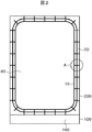
図1は本発明が適用される液晶表示装置の例を示す平面図である。図1において、走査線50や映像信号線60が形成されたTFT基板100と、対向基板200とが周辺に形成されたシール材150によって接着し、内部に液晶が挟持されている。TFT基板100と対向基板200が重なった部分に表示領域80が形成され、表示領域80の外側が額縁領域になっている。
FIG. 1 is a plan view showing an example of a liquid crystal display device to which the present invention is applied. In FIG. 1, the
TFT基板100は対向基板200よりも大きく形成され、TFT基板100が1枚になった部分が端子部160になっている。端子部160には、表示領域80に走査信号、映像信号、電源等を供給するための端子が形成され、また、液晶を駆動するためにICドライバが配置される。さらに、端子部160には、外部から信号や電源を供給するために、いわゆるフレキシブル配線基板が接続される。
The
図1において、表示領域80には、走査線50が横方向に延在し、縦方向に配列している。また、映像信号線60が縦方向に延在し、横方向に配列している。走査信号、映像信号等は、端子部から供給される。走査線50と映像信号線60で囲まれた領域が画素70になっている。各画素70は、TFTと画素電極を含んでいる。近年、額縁領域を狭くすることが求められており、図1に示す幅waは、0.5mm程度になっている。そうすると、額縁領域に形成されるシール材150の幅も狭くなり、図1に示す幅wbは、0.3mm程度になっている。
In FIG. 1, in the
シール材150はディスペンサによって塗布されるが、シール材150の幅が小さくなると、塗布のばらつきがシール部の信頼性に大きく影響してくる。図2(A)は、シール材150が一部で狭くなり、途切れてしまった例である。シール材150の幅がもともと大きければ、途切れるようなことは無いが、図2(A)のような現象は、シール材150の幅が狭くなったことに起因する。
The sealing
図2(B)は、シール材150の塗布位置がばらつき、かつ、その部分でシール材150の幅が大きくなった場合であり、シール材150が表示領域80にまではみ出している例である。このような現象は、額縁領域の幅が大きければ生じにくいが、額縁領域が狭くなったことによって生じやすくなっている。なお、シール材は印刷等によって塗布される場合もあるが、同様な問題が生ずる。本発明の課題の一つは、このような現象を対策するものである。以下に実施例によって本発明を詳細に説明する。
FIG. 2B shows an example in which the application position of the sealing
図3は本発明を示す平面模式図である。図3において、TFT基板100の上に対向基板200が配置し、内部に液晶が封止されている。シール部において、対向基板200側には、一部が平面で視てT字型になっている突起10が対向基板200の周辺全周に形成されている。この突起10は、一部が平面で視てT字型になっているので、以後T字型突起10と呼ぶ。一方、TFT基板100側には、周辺に、枠状に突起20が形成されている。以後これを枠状突起20と呼ぶ。図3では、図を複雑にしないために、シール材は省略されている。
FIG. 3 is a schematic plan view showing the present invention. In FIG. 3, the
図4は、図3のA部の斜視図である。図4では、図をわかりやすくするために、シール材は省略されている。図4において、T字型突起10は、対向基板200側に形成され、枠状突起20はTFT基板100側に形成されている。T字型突起10も枠状突起20も断面が3角形となっている。T字型突起10と枠状突起20とは、3角形の頂点において接触している。図4において、T字型突起10の高さh1と枠状突起20の高さh2の和h1+h2がTFT基板100と対向基板200の間隔となっている。h1=h2である場合が多い。この場合、TFT基板100と対向基板200の間隔が3μmであれば、h1、h2は各々1.5μm程度である。このように、T字型突起10と枠状突起20はシール部におけるスペーサとしての役割も有している。
FIG. 4 is a perspective view of part A in FIG. In FIG. 4, the sealing material is omitted for easy understanding of the drawing. In FIG. 4, the T-shaped
T字型突起10、枠状突起20の底部の幅については、以後単に幅という。T字型突起10の、対向基板200の辺と平行な方向な部分の幅w11、対向基板200の辺と垂直な方向に延在する部分の幅w1、枠状突起10の底部の幅w2(以後単に幅という)は各々、例えば15μm程度である。シール材の幅は300μm程度であるから、w1、w11、w2はシール材の幅に比べれば問題にならない。なお、T字型突起10の、対向基板200の辺と直角方向に延在する方向の幅w5は、シール材の幅と同程度かそれよりも小さくてもよい。T字型突起10も枠状突起20もフォトリソグラフィで形成するので、正確な寸法で形成することが出来る。
The widths of the bottoms of the T-shaped
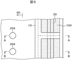
図5は図3のA部の平面図である。図5は対向基板200側から見た図である。対向基板200側にT字型突起10が形成されており、TFT基板側100に枠状突起20が形成されている。T字型突起10における中心の点線は、3角形の頂点を表している。点線となっているのは、平面で視て、裏側に3角形の頂点があるからである。枠状突起20の中心の線は枠状突起の3角形の頂点を表している。T字型突起10と枠状突起20の間にシール材150が充填されている。図5において、左側は表示領域80となっており、この領域には、TFT基板100と対向基板200の間隔を保持するための柱状スペーサ204が形成されている。
FIG. 5 is a plan view of a portion A in FIG. FIG. 5 is a view seen from the
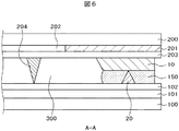
図6は図5のA−A断面図である。図6において、TFT基板100の上には、有機パッシベーション膜101が形成されている。有機パッシベーション膜101は、例えばアクリル等の透明樹脂で形成されている。有機パッシベーション膜101の下には、TFT、絶縁膜等他の層が形成されているが、図6では図を複雑化しないために省略されている。有機絶縁膜はTFTを保護するとともに、平坦化膜としても使用されるので、1乃至4μm程度と、厚く形成される。有機パッシベーション膜101の上には、無機絶縁膜102が形成されている。この無機絶縁膜102の上に、枠状突起20が形成されている。
6 is a cross-sectional view taken along the line AA in FIG. In FIG. 6, an
図6において、TFT基板100と対向して対向基板200が配置している。対向基板200にはシール部では遮光膜となるブラックマトリクス201が形成され、表示領域80においては、カラーフィルタ202が形成されている。ブラックマトリクス201およびカラーフィルタ202を覆ってオーバーコート膜203が形成されている。オーバーコート膜203の上にシール部ではT字型突起10が形成され、表示領域80では柱状スペーサ204が形成されている。TFT基板100と対向基板200はシール材によって接着している。
In FIG. 6, a
図6において、シール材150よりも内側には、液晶300が充填されている。液晶300はTFT基板100側および対向基板200側に形成された配向膜によって初期配向を受けるが、図6では、図を複雑化しないために配向膜は省略されている。図6に示すように、シール部におけるTFT基板100と対向基板200の間隔は、T字型突起10と枠状突起20によって規定されており、表示領域80においては、柱状スペーサ204によって規定されている。
In FIG. 6, the
本実施例では、液晶300は滴下方式によって内部に充填されるが、液晶を滴下する時は、シール材150はまだ硬化していない。シール材150が硬化していない状態で、液晶300とシール材150が接すると、シール材150の成分が液晶300内に溶け込むことになり、液晶の特性を低下させる場合がある。本発明においては、図6に示すように、シール材150が液晶と接する面積は、T字型突起10がある分、小さくなっている。したがって、硬化前にシール材150が液晶を汚染する機会は従来構造に比較して小さくなっている。
In this embodiment, the
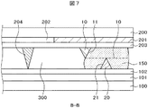
図7は図5のB−B断面図である。図7はシール部を除いて図6と同様である。図7において、シール材150がTFT基板100と対向基板200を接着している。T字型突起10の点線は、T字型突起10がシール材150の裏側に隠れていることを示している。図7に示すように、シール材150は、T字型突起10の3角形の斜面11、あるいは、枠状突起20の3角形の斜面21と接する分、接触面積が大きくなっているので、シール材150による接着力を向上することが出来、シール部の信頼性が向上する。その他の構成は、図6で説明したとおりである。
7 is a cross-sectional view taken along line BB in FIG. FIG. 7 is the same as FIG. 6 except for the seal portion. In FIG. 7, the sealing
図8は、本発明における製造方法を実施例1の構成を例にとって説明する模式図である。図8(A)は対向基板200側であり、図8(B)はTFT基板100側である。図8(A)において、対向基板200側にT字型突起10を形成する。T字型突起10は、表示領域において、柱状スペーサを形成する時に同時に、同じ材料を用いて形成することが出来る。T字型突起10の高さは柱状スペーサの高さよりも低いので、例えば、ハーフ露光技術を用いて形成することが出来る。
FIG. 8 is a schematic diagram illustrating the manufacturing method according to the present invention, taking the configuration of the first embodiment as an example. 8A shows the
T字型突起10は、オーバーコート膜203を形成する時に、ハーフ露光技術を用いてT字型突起10に対応する部分のオーバーコート膜の膜厚を他の領域におけるよりも大きくすることによっても形成することが出来る。その後、T字型突起10の上にシール材150をディスペンサによって塗布する。その後、T字型突起10で囲まれた領域内に液晶301を滴下する。この状態ではシール材150はまだ硬化していない。しかし、T字型突起10によって液晶301とシール材150とが区画されているので、液晶301のシール材150による汚染は抑制することが出来る。
When the
図8(B)は、TFT基板100側に枠状突起20を形成した状態を示している。枠状突起20は、無機絶縁膜の上に例えば有機パッシベーション膜と同じ材料によって形成することが出来るが、他の有機材料でもよい。あるいは、ハーフ露光技術を用いることによって、枠状突起20に対応する部分の有機パッシベーション膜の膜厚を他の領域におけるよりも大きくすることによって、枠状突起20を形成することも出来る。
FIG. 8B shows a state in which a frame-
その後、TFT基板100と対向基板200をシール材150を介して貼りあわせる。この時、シール材150は、T字型突起10と枠状突起20によって押し広げられるので、図2(A)に示すような、シール材150の途切れは防ぐことが出来る。また、図2(B)に示すようなシール材150の表示領域80へのはみだしに対しては、T字型突起10の存在によって抑制することが出来る。また、シール材150の外側へのはみだしも枠状突起20の存在によって抑制することが出来る。
Thereafter, the
図9は、本発明における製造方法の他の例である。図9が図8と異なる点は、図9では対向基板200側に枠状突起20を形成し、TFT基板100側にT字型突起10を形成している点である。TFT基板100のT字型突起10は、図8で説明したのと同様に形成することが出来る。図9においては、TFT基板100側にシール材150が形成され、液晶301が滴下される。
FIG. 9 shows another example of the manufacturing method in the present invention. 9 differs from FIG. 8 in that a frame-
一方、枠状突起20は対向基板200側に形成される。この場合の枠状突起20は、図8で説明したT字型突起10を形成するのと同様にして形成することが出来る。その後、TFT基板100と対向基板200をシール材150を介して貼りあわせる。この時、シール材150は、T字型突起10と枠状突起20によって押し広げられるので、図2(A)に示すような、シール材20の途切れは防ぐことが出来る。また、図2(B)に示すようなシール材20の表示領域へのはみだしに対しては、T字型突起10の存在によって抑制することが出来る。また、シール材150の外側へのはみだしも枠状突起10の存在によって抑制することが出来る。
On the other hand, the frame-shaped
以上の説明では、T字型突起10、枠状突起20、柱状スペーサ204等の断面は、3角形であるとして説明したが、本発明はこれに限る必要はない。図10はT字型突起10、枠状突起20、柱状スペーサ204等の断面が台形の場合である。この場合も、以上で説明した効果を得ることが出来る。図11は、T字型突起10、枠状突起20、柱状スペーサ204等の断面が蒲鉾状である場合の例である。この場合も同様な効果を得ることが出来る。
In the above description, the cross sections of the T-shaped
図12は実施例2を示す平面模式図である。図12が実施例1の図3と異なる点は、TFT基板側100に枠状突起20が並行して2本形成されている点である。枠状突起20を2本形成することによって、TFT基板100と対向基板200を貼りあわせた時に、シール材150をより均一に広げることが出来る。その他の構成は図3で説明したのと同様である。
FIG. 12 is a schematic plan view showing the second embodiment. FIG. 12 differs from FIG. 3 of the first embodiment in that two frame-shaped
図13は、図12のB部の斜視図である。図で13は、図をわかりやすくするために、シール材は省略されている。図13が実施例1の図4と異なる点は、TFT基板100側に枠状突起10が2本形成されていることである。そして、2本の枠状突起20の3角形の頂点がT字型突起10の3角形の頂点と接触している。図13における、T字型突起10の幅w1、w11と2本の枠状突起10の各々の幅w2は各々15μmであり、図4で説明したのと同様である。また、T字型突起10の高さh1、枠状突起20の高さh2も図4で説明したのと同様である。
FIG. 13 is a perspective view of a portion B in FIG. In FIG. 13, the seal material is omitted for the sake of clarity. FIG. 13 differs from FIG. 4 of the first embodiment in that two frame-
図14は図12のB部の平面図である。図12は対向基板200側から見た図である。図14が実施例1の図5と異なる点は、TFT基板100側に枠状突起20が2本形成されている点である。シール材150の幅は300μm程度であるのに対し、枠状突起20の幅は15μm程度なので、枠状突起20を2本配置してもスペース的には問題ない。その他の構成は図5と同様である。
FIG. 14 is a plan view of a portion B in FIG. FIG. 12 is a view seen from the
図15は、図14のC−C断面図である。図15が実施例1の図6と異なる点は、枠状突起20が並行して2本形成され、いずれもがT字型突起10と接している点である。枠状突起20が2本存在することによって、シール部におけるTFT基板100と対向基板200の間隔をより安定して保持することが出来る。
15 is a cross-sectional view taken along the line CC of FIG. FIG. 15 differs from FIG. 6 of the first embodiment in that two frame-shaped
図16は図14のD−D断面図である。図16が実施例1の図7と異なる点は、2個の枠状突起20がT字型突起10と接していることである。図16に示すように、2本の枠状突起20の3角形の斜面21、T字型突起10の3角形の斜面11がシール材150と接着しているので、実施例1の場合よりもさらにシール材150の接着強度を上げることが出来る。
16 is a cross-sectional view taken along the line DD of FIG. 16 differs from FIG. 7 of the first embodiment in that two frame-shaped
本実施例の他の構成および効果は実施例1で説明したのと同様である。 Other configurations and effects of the present embodiment are the same as those described in the first embodiment.
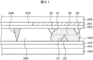
図17は実施例3を示す平面模式図である。図17が実施例1の図3と異なる点は、対向基板200側にT字型突起ではなく、H字型突起30が周辺に形成されている点である。TFT基板100側には、H字型突起30のブリッジ部の中央部を横切るようにTFT基板100の辺と平行に枠状突起20が形成されている。枠状突起20は実施例1における枠状突起20と同様である。H字型突起30はブリッジ部において、枠状突起と接している。
FIG. 17 is a schematic plan view showing the third embodiment. FIG. 17 differs from FIG. 3 of the first embodiment in that an H-shaped
図18は、図17のC部の斜視図である。図17では、シール材は省略されている。図18において、H字型突起30の断面は、頂点が下側である3角形である。TFT基板100に形成された枠状突起20の断面である3角形の頂点がH字型突起30のブリッジ部と接触している。図18において、H字型突起30の対向基板200の辺と平行な部分の幅w31とH字型突起30のブリッジ部の幅w3、枠状突起20の幅w2はいずれも15μm程度である。H字型突起30、枠状突起20の高さは、実施例1におけるT字型突起10、枠状突起20と同様である。
18 is a perspective view of a portion C in FIG. In FIG. 17, the sealing material is omitted. In FIG. 18, the cross section of the H-shaped
図19は図17のC部の平面図である。図19において、H字型突起30の内部領域にシール材150が配置されている。図19におけるH字型突起30の中心線である点線は、裏側に存在している3角形の断面の頂点を表している。TFT基板100に形成された枠状突起20の頂点は、H字型突起30のブリッジ部の中央付近において、H字型突起30の頂点と接している。
FIG. 19 is a plan view of a portion C in FIG. In FIG. 19, a sealing
図20は、図19のE−E断面図である。図20において、対向基板200に形成されたH字型突起30のブリッジ部がTFT基板100に形成された枠状突起20と接している。これによってTFT基板100と対向基板200の間隔を維持している。図20のその他の構成は、実施例1の図6と同様である。
20 is a cross-sectional view taken along line EE in FIG. In FIG. 20, the bridge portion of the H-shaped
図21は、図19のF−F断面図である。図21におけるH字型突起30の点線は、H字型突起30のブリッジ部がシール材150に隠れていることを示している。図21において、TFT基板100に形成された枠状突起10の先端が、H字型突起30と接している。図21において、対向基板200に形成されたH字型突起30の断面の3角形の斜面、および、TFT基板100に形成された枠状突起20の断面の3角形の斜面において、シール材150の接着面積が大きくなるので、接着力が向上し、シール部の信頼性を向上させることが出来る。
21 is a cross-sectional view taken along line FF in FIG. A dotted line of the H-shaped
実施例1乃至3では、T字型突起、枠状突起、H字型突起はTFT基板あるいは対向基板の全周に形成されているとして説明したが、これに限らず、基板の辺に沿って飛び飛びに形成しても効果を上げることが出来る。また、シール材の幅等の制御が比較的難しい、基板のコーナー部に対応する位置のみに形成してもよい。 In the first to third embodiments, it has been described that the T-shaped protrusion, the frame-shaped protrusion, and the H-shaped protrusion are formed on the entire circumference of the TFT substrate or the counter substrate. The effect can be improved even if it is formed in a flying shape. Further, it may be formed only at a position corresponding to a corner portion of the substrate where the control of the width or the like of the sealing material is relatively difficult.
また、図9において説明したように、本発明は、TFT基板側にT字型突起あるいはH字型突起を形成し、対向基板側に枠状突起を形成した構成であってもよい。 Further, as described with reference to FIG. 9, the present invention may have a configuration in which a T-shaped protrusion or an H-shaped protrusion is formed on the TFT substrate side and a frame-shaped protrusion is formed on the counter substrate side.
10…T字型突起、11…T字型突起の斜面、 20…枠状突起、 21…枠状突起の斜面、 30…H字型突起、 31…H字型突起の斜面、 50…走査線、 60…映像信号線、 70…画素、 80…表示領域、 100…TFT基板、 101…有機パッシベーション膜、 102…無機絶縁膜、 150…シール材、 160…端子部、 200…対向基板、 201…ブラックマトリクス、 202…カラーフィルタ、 203…オーバーコート膜、 204…柱状スペーサ、 300…液晶、 301…滴下液晶
DESCRIPTION OF
Claims (9)
前記第1の基板は、前記第1の基板の周辺において、前記第1の基板の辺に沿って延在する第1の部分と、前記第1の部分から、前記第1の基板の端部に向かって延在する第2の部分が形成された第1の突起を有し、
前記第1の突起の断面の幅は、前記第1の基板側よりも先端側で小さく、
前記第2の基板は、前記第2の基板の周辺において、前記第1の基板の辺に沿って延在する第2突起を有し、
前記第2の突起の断面の幅は、前記第2の基板側よりも先端側で小さく、
前記第1の突起の前記第2の部分は、前記第2の突起と対向し、
前記第1の突起と前記第2の突起の間には、前記シール材が存在していることを特徴とする液晶表示装置。 A liquid crystal display device in which a first substrate and a second substrate are bonded by a sealing material in the periphery, and liquid crystal is sealed inside,
The first substrate includes a first portion extending along a side of the first substrate at a periphery of the first substrate, and an end portion of the first substrate from the first portion. A first protrusion formed with a second portion extending toward the
The width of the cross section of the first protrusion is smaller on the tip side than on the first substrate side,
The second substrate has a second protrusion extending along a side of the first substrate at a periphery of the second substrate;
The width of the cross section of the second protrusion is smaller on the tip side than on the second substrate side,
The second portion of the first protrusion is opposed to the second protrusion;
The liquid crystal display device, wherein the sealing material exists between the first protrusion and the second protrusion.
前記第2の突起は、前記第2の基板の辺に沿って全周に形成されていることを特徴とする請求項1に記載の液晶表示装置。 The first protrusion is formed on the entire circumference along the side of the first substrate,
The liquid crystal display device according to claim 1, wherein the second protrusion is formed on the entire circumference along the side of the second substrate.
Priority Applications (2)
| Application Number | Priority Date | Filing Date | Title |
|---|---|---|---|
| JP2015253793A JP2017116797A (en) | 2015-12-25 | 2015-12-25 | Liquid crystal display device |
| US15/344,657 US20170184899A1 (en) | 2015-12-25 | 2016-11-07 | Liquid crystal display device |
Applications Claiming Priority (1)
| Application Number | Priority Date | Filing Date | Title |
|---|---|---|---|
| JP2015253793A JP2017116797A (en) | 2015-12-25 | 2015-12-25 | Liquid crystal display device |
Publications (1)
| Publication Number | Publication Date |
|---|---|
| JP2017116797A true JP2017116797A (en) | 2017-06-29 |
Family
ID=59086215
Family Applications (1)
| Application Number | Title | Priority Date | Filing Date |
|---|---|---|---|
| JP2015253793A Pending JP2017116797A (en) | 2015-12-25 | 2015-12-25 | Liquid crystal display device |
Country Status (2)
| Country | Link |
|---|---|
| US (1) | US20170184899A1 (en) |
| JP (1) | JP2017116797A (en) |
Cited By (1)
| Publication number | Priority date | Publication date | Assignee | Title |
|---|---|---|---|---|
| JP2020034604A (en) * | 2018-08-27 | 2020-03-05 | 株式会社ジャパンディスプレイ | Display |
Families Citing this family (4)
| Publication number | Priority date | Publication date | Assignee | Title |
|---|---|---|---|---|
| JP6606432B2 (en) * | 2016-01-06 | 2019-11-13 | 株式会社ジャパンディスプレイ | Display device and manufacturing method thereof |
| CN107589573A (en) * | 2017-08-25 | 2018-01-16 | 惠科股份有限公司 | Liquid crystal display panel and liquid crystal display device |
| US10756297B2 (en) * | 2018-04-19 | 2020-08-25 | Wuhan China Star Optoelectronics Semiconductor Display Technology Co., Ltd. | Flexible panel, manufacturing method for the same and display device |
| CN110554530A (en) * | 2018-06-04 | 2019-12-10 | 鸿富锦精密工业(深圳)有限公司 | Display panel and display device |
Family Cites Families (8)
| Publication number | Priority date | Publication date | Assignee | Title |
|---|---|---|---|---|
| JP3098515B1 (en) * | 1999-08-13 | 2000-10-16 | インターナショナル・ビジネス・マシーンズ・コーポレ−ション | Liquid crystal display device, liquid crystal display device with narrow frame, and method of manufacturing liquid crystal display device |
| JP4723283B2 (en) * | 2005-05-19 | 2011-07-13 | シチズンホールディングス株式会社 | Manufacturing method of liquid crystal panel |
| TWI345652B (en) * | 2006-12-01 | 2011-07-21 | Chimei Innolux Corp | Liquid crystal panel and method of manufacturing the same |
| JP2010139953A (en) * | 2008-12-15 | 2010-06-24 | Hitachi Displays Ltd | Liquid crystal display device |
| JP2014119705A (en) * | 2012-12-19 | 2014-06-30 | Sony Corp | Moisture-proof structure and display device |
| JP5961543B2 (en) * | 2012-12-19 | 2016-08-02 | 株式会社ジャパンディスプレイ | Liquid crystal display device and manufacturing method thereof |
| JP2015022120A (en) * | 2013-07-18 | 2015-02-02 | 株式会社ジャパンディスプレイ | Display element and manufacturing method of the same |
| JP2015025905A (en) * | 2013-07-25 | 2015-02-05 | 株式会社ジャパンディスプレイ | Liquid crystal display device |
-
2015
- 2015-12-25 JP JP2015253793A patent/JP2017116797A/en active Pending
-
2016
- 2016-11-07 US US15/344,657 patent/US20170184899A1/en not_active Abandoned
Cited By (2)
| Publication number | Priority date | Publication date | Assignee | Title |
|---|---|---|---|---|
| JP2020034604A (en) * | 2018-08-27 | 2020-03-05 | 株式会社ジャパンディスプレイ | Display |
| JP7282490B2 (en) | 2018-08-27 | 2023-05-29 | 株式会社ジャパンディスプレイ | Display device |
Also Published As
| Publication number | Publication date |
|---|---|
| US20170184899A1 (en) | 2017-06-29 |
Similar Documents
| Publication | Publication Date | Title |
|---|---|---|
| JP6491825B2 (en) | Liquid crystal display | |
| US9759955B2 (en) | Liquid crystal display device | |
| JP5520614B2 (en) | Liquid crystal display device and manufacturing method thereof | |
| JP6347937B2 (en) | Liquid crystal display | |
| US10054823B2 (en) | Liquid crystal display device | |
| JP5384982B2 (en) | Liquid crystal display | |
| JP6132503B2 (en) | Liquid crystal display | |
| JP6220592B2 (en) | Liquid crystal display element and manufacturing method thereof | |
| JP2017116797A (en) | Liquid crystal display device | |
| US10042213B2 (en) | Display device including projections opposed to each other in a sealant | |
| JP2017090528A (en) | Display | |
| JP6649788B2 (en) | Liquid crystal display | |
| JP2010096856A (en) | Liquid crystal display device | |
| JP5538106B2 (en) | LCD panel | |
| JP2018054733A (en) | Liquid crystal display device and color filter substrate | |
| JP2017090794A (en) | Liquid crystal display device | |
| JP2009168832A (en) | Liquid crystal display and method of manufacturing the same | |
| JP5042467B2 (en) | Liquid crystal display device and liquid crystal panel | |
| JP2017122790A (en) | Liquid crystal display device | |
| US11022846B2 (en) | Substrate for display device and display device | |
| JP6035081B2 (en) | Liquid crystal display | |
| JP2010175727A (en) | Liquid crystal display device | |
| JP6739564B2 (en) | Liquid crystal display | |
| JP6367415B2 (en) | Liquid crystal display | |
| JP2017067829A (en) | Liquid crystal display |