JP2017116630A - Wavelength conversion device, illumination device and projector - Google Patents
Wavelength conversion device, illumination device and projector Download PDFInfo
- Publication number
- JP2017116630A JP2017116630A JP2015249404A JP2015249404A JP2017116630A JP 2017116630 A JP2017116630 A JP 2017116630A JP 2015249404 A JP2015249404 A JP 2015249404A JP 2015249404 A JP2015249404 A JP 2015249404A JP 2017116630 A JP2017116630 A JP 2017116630A
- Authority
- JP
- Japan
- Prior art keywords
- wavelength conversion
- light
- region
- base material
- wavelength
- Prior art date
- Legal status (The legal status is an assumption and is not a legal conclusion. Google has not performed a legal analysis and makes no representation as to the accuracy of the status listed.)
- Withdrawn
Links
Images


Classifications
-
- G—PHYSICS
- G03—PHOTOGRAPHY; CINEMATOGRAPHY; ANALOGOUS TECHNIQUES USING WAVES OTHER THAN OPTICAL WAVES; ELECTROGRAPHY; HOLOGRAPHY
- G03B—APPARATUS OR ARRANGEMENTS FOR TAKING PHOTOGRAPHS OR FOR PROJECTING OR VIEWING THEM; APPARATUS OR ARRANGEMENTS EMPLOYING ANALOGOUS TECHNIQUES USING WAVES OTHER THAN OPTICAL WAVES; ACCESSORIES THEREFOR
- G03B21/00—Projectors or projection-type viewers; Accessories therefor
- G03B21/14—Details
- G03B21/20—Lamp housings
- G03B21/2006—Lamp housings characterised by the light source
- G03B21/2033—LED or laser light sources
- G03B21/204—LED or laser light sources using secondary light emission, e.g. luminescence or fluorescence
-
- F—MECHANICAL ENGINEERING; LIGHTING; HEATING; WEAPONS; BLASTING
- F21—LIGHTING
- F21K—NON-ELECTRIC LIGHT SOURCES USING LUMINESCENCE; LIGHT SOURCES USING ELECTROCHEMILUMINESCENCE; LIGHT SOURCES USING CHARGES OF COMBUSTIBLE MATERIAL; LIGHT SOURCES USING SEMICONDUCTOR DEVICES AS LIGHT-GENERATING ELEMENTS; LIGHT SOURCES NOT OTHERWISE PROVIDED FOR
- F21K9/00—Light sources using semiconductor devices as light-generating elements, e.g. using light-emitting diodes [LED] or lasers
- F21K9/60—Optical arrangements integrated in the light source, e.g. for improving the colour rendering index or the light extraction
- F21K9/64—Optical arrangements integrated in the light source, e.g. for improving the colour rendering index or the light extraction using wavelength conversion means distinct or spaced from the light-generating element, e.g. a remote phosphor layer
-
- F—MECHANICAL ENGINEERING; LIGHTING; HEATING; WEAPONS; BLASTING
- F21—LIGHTING
- F21V—FUNCTIONAL FEATURES OR DETAILS OF LIGHTING DEVICES OR SYSTEMS THEREOF; STRUCTURAL COMBINATIONS OF LIGHTING DEVICES WITH OTHER ARTICLES, NOT OTHERWISE PROVIDED FOR
- F21V13/00—Producing particular characteristics or distribution of the light emitted by means of a combination of elements specified in two or more of main groups F21V1/00 - F21V11/00
- F21V13/12—Combinations of only three kinds of elements
- F21V13/14—Combinations of only three kinds of elements the elements being filters or photoluminescent elements, reflectors and refractors
-
- F—MECHANICAL ENGINEERING; LIGHTING; HEATING; WEAPONS; BLASTING
- F21—LIGHTING
- F21V—FUNCTIONAL FEATURES OR DETAILS OF LIGHTING DEVICES OR SYSTEMS THEREOF; STRUCTURAL COMBINATIONS OF LIGHTING DEVICES WITH OTHER ARTICLES, NOT OTHERWISE PROVIDED FOR
- F21V9/00—Elements for modifying spectral properties, polarisation or intensity of the light emitted, e.g. filters
- F21V9/30—Elements containing photoluminescent material distinct from or spaced from the light source
- F21V9/32—Elements containing photoluminescent material distinct from or spaced from the light source characterised by the arrangement of the photoluminescent material
-
- F—MECHANICAL ENGINEERING; LIGHTING; HEATING; WEAPONS; BLASTING
- F21—LIGHTING
- F21V—FUNCTIONAL FEATURES OR DETAILS OF LIGHTING DEVICES OR SYSTEMS THEREOF; STRUCTURAL COMBINATIONS OF LIGHTING DEVICES WITH OTHER ARTICLES, NOT OTHERWISE PROVIDED FOR
- F21V9/00—Elements for modifying spectral properties, polarisation or intensity of the light emitted, e.g. filters
- F21V9/40—Elements for modifying spectral properties, polarisation or intensity of the light emitted, e.g. filters with provision for controlling spectral properties, e.g. colour, or intensity
- F21V9/45—Elements for modifying spectral properties, polarisation or intensity of the light emitted, e.g. filters with provision for controlling spectral properties, e.g. colour, or intensity by adjustment of photoluminescent elements
-
- G—PHYSICS
- G02—OPTICS
- G02B—OPTICAL ELEMENTS, SYSTEMS OR APPARATUS
- G02B27/00—Optical systems or apparatus not provided for by any of the groups G02B1/00 - G02B26/00, G02B30/00
- G02B27/09—Beam shaping, e.g. changing the cross-sectional area, not otherwise provided for
- G02B27/0905—Dividing and/or superposing multiple light beams
-
- G—PHYSICS
- G02—OPTICS
- G02B—OPTICAL ELEMENTS, SYSTEMS OR APPARATUS
- G02B27/00—Optical systems or apparatus not provided for by any of the groups G02B1/00 - G02B26/00, G02B30/00
- G02B27/09—Beam shaping, e.g. changing the cross-sectional area, not otherwise provided for
- G02B27/0938—Using specific optical elements
- G02B27/095—Refractive optical elements
- G02B27/0955—Lenses
- G02B27/0961—Lens arrays
-
- G—PHYSICS
- G02—OPTICS
- G02B—OPTICAL ELEMENTS, SYSTEMS OR APPARATUS
- G02B27/00—Optical systems or apparatus not provided for by any of the groups G02B1/00 - G02B26/00, G02B30/00
- G02B27/10—Beam splitting or combining systems
- G02B27/1006—Beam splitting or combining systems for splitting or combining different wavelengths
-
- G—PHYSICS
- G02—OPTICS
- G02B—OPTICAL ELEMENTS, SYSTEMS OR APPARATUS
- G02B27/00—Optical systems or apparatus not provided for by any of the groups G02B1/00 - G02B26/00, G02B30/00
- G02B27/10—Beam splitting or combining systems
- G02B27/14—Beam splitting or combining systems operating by reflection only
- G02B27/141—Beam splitting or combining systems operating by reflection only using dichroic mirrors
-
- G—PHYSICS
- G02—OPTICS
- G02B—OPTICAL ELEMENTS, SYSTEMS OR APPARATUS
- G02B5/00—Optical elements other than lenses
- G02B5/30—Polarising elements
- G02B5/3083—Birefringent or phase retarding elements
-
- G—PHYSICS
- G03—PHOTOGRAPHY; CINEMATOGRAPHY; ANALOGOUS TECHNIQUES USING WAVES OTHER THAN OPTICAL WAVES; ELECTROGRAPHY; HOLOGRAPHY
- G03B—APPARATUS OR ARRANGEMENTS FOR TAKING PHOTOGRAPHS OR FOR PROJECTING OR VIEWING THEM; APPARATUS OR ARRANGEMENTS EMPLOYING ANALOGOUS TECHNIQUES USING WAVES OTHER THAN OPTICAL WAVES; ACCESSORIES THEREFOR
- G03B21/00—Projectors or projection-type viewers; Accessories therefor
- G03B21/005—Projectors using an electronic spatial light modulator but not peculiar thereto
-
- G—PHYSICS
- G03—PHOTOGRAPHY; CINEMATOGRAPHY; ANALOGOUS TECHNIQUES USING WAVES OTHER THAN OPTICAL WAVES; ELECTROGRAPHY; HOLOGRAPHY
- G03B—APPARATUS OR ARRANGEMENTS FOR TAKING PHOTOGRAPHS OR FOR PROJECTING OR VIEWING THEM; APPARATUS OR ARRANGEMENTS EMPLOYING ANALOGOUS TECHNIQUES USING WAVES OTHER THAN OPTICAL WAVES; ACCESSORIES THEREFOR
- G03B21/00—Projectors or projection-type viewers; Accessories therefor
- G03B21/14—Details
- G03B21/16—Cooling; Preventing overheating
-
- G—PHYSICS
- G03—PHOTOGRAPHY; CINEMATOGRAPHY; ANALOGOUS TECHNIQUES USING WAVES OTHER THAN OPTICAL WAVES; ELECTROGRAPHY; HOLOGRAPHY
- G03B—APPARATUS OR ARRANGEMENTS FOR TAKING PHOTOGRAPHS OR FOR PROJECTING OR VIEWING THEM; APPARATUS OR ARRANGEMENTS EMPLOYING ANALOGOUS TECHNIQUES USING WAVES OTHER THAN OPTICAL WAVES; ACCESSORIES THEREFOR
- G03B21/00—Projectors or projection-type viewers; Accessories therefor
- G03B21/14—Details
- G03B21/20—Lamp housings
- G03B21/2006—Lamp housings characterised by the light source
- G03B21/2013—Plural light sources
-
- F—MECHANICAL ENGINEERING; LIGHTING; HEATING; WEAPONS; BLASTING
- F21—LIGHTING
- F21Y—INDEXING SCHEME ASSOCIATED WITH SUBCLASSES F21K, F21L, F21S and F21V, RELATING TO THE FORM OR THE KIND OF THE LIGHT SOURCES OR OF THE COLOUR OF THE LIGHT EMITTED
- F21Y2115/00—Light-generating elements of semiconductor light sources
- F21Y2115/30—Semiconductor lasers
-
- G—PHYSICS
- G02—OPTICS
- G02B—OPTICAL ELEMENTS, SYSTEMS OR APPARATUS
- G02B19/00—Condensers, e.g. light collectors or similar non-imaging optics
- G02B19/0004—Condensers, e.g. light collectors or similar non-imaging optics characterised by the optical means employed
- G02B19/0009—Condensers, e.g. light collectors or similar non-imaging optics characterised by the optical means employed having refractive surfaces only
-
- G—PHYSICS
- G02—OPTICS
- G02B—OPTICAL ELEMENTS, SYSTEMS OR APPARATUS
- G02B27/00—Optical systems or apparatus not provided for by any of the groups G02B1/00 - G02B26/00, G02B30/00
- G02B27/10—Beam splitting or combining systems
- G02B27/14—Beam splitting or combining systems operating by reflection only
- G02B27/149—Beam splitting or combining systems operating by reflection only using crossed beamsplitting surfaces, e.g. cross-dichroic cubes or X-cubes
-
- G—PHYSICS
- G02—OPTICS
- G02B—OPTICAL ELEMENTS, SYSTEMS OR APPARATUS
- G02B27/00—Optical systems or apparatus not provided for by any of the groups G02B1/00 - G02B26/00, G02B30/00
- G02B27/28—Optical systems or apparatus not provided for by any of the groups G02B1/00 - G02B26/00, G02B30/00 for polarising
- G02B27/283—Optical systems or apparatus not provided for by any of the groups G02B1/00 - G02B26/00, G02B30/00 for polarising used for beam splitting or combining
-
- G—PHYSICS
- G02—OPTICS
- G02B—OPTICAL ELEMENTS, SYSTEMS OR APPARATUS
- G02B5/00—Optical elements other than lenses
- G02B5/02—Diffusing elements; Afocal elements
- G02B5/0273—Diffusing elements; Afocal elements characterized by the use
- G02B5/0284—Diffusing elements; Afocal elements characterized by the use used in reflection
Abstract
Description
本発明は、波長変換装置、照明装置及びプロジェクターに関する。 The present invention relates to a wavelength conversion device, an illumination device, and a projector.
従来、固体光源から出射された励起光を波長変換し、蛍光として出射する光源装置が知られている(例えば、特許文献1参照)。
この特許文献1に記載の光源装置は、固体光源及び反射型蛍光回転体を備える。これらのうち、反射型蛍光体回転体は、蛍光体層と、当該蛍光体層が接合部材により固定される放熱部材とを備える。この蛍光体層は、固体光源から出射された励起光の一部を励起光とは異なる波長の光に変換して蛍光を生成する。
2. Description of the Related Art Conventionally, a light source device that converts the wavelength of excitation light emitted from a solid light source and emits it as fluorescence is known (for example, see Patent Document 1).
The light source device described in
ところで、蛍光体層の温度が上昇した場合に、固体光源から入射された光の波長変換効率が低下することが知られている。このため、特許文献1に記載の反射型蛍光回転体のような波長変換装置では、放熱部材を回転させ、当該放熱部材上に形成された蛍光体層を冷却している。
しかしながら、特許文献1に記載の波長変換装置では、放熱部材(基板)の光入射側の領域の略全領域に蛍光体層が形成されているので、当該放熱部材を回転させたとしても、当該蛍光体層の熱を放熱する放熱面積が不足していることから、蛍光体層の温度が上昇しやすく、かつ、当該放熱部材により当該蛍光体層の熱を確実に放熱できないことがある。すなわち、特許文献1に記載の波長変換装置では、波長変換効率の低下が生じない程度に蛍光体層を冷却することができないので、当該蛍光体層による波長変換効率が低下するという問題がある。
By the way, it is known that when the temperature of the phosphor layer rises, the wavelength conversion efficiency of the light incident from the solid light source decreases. For this reason, in the wavelength conversion device such as the reflection type fluorescent rotator described in
However, in the wavelength conversion device described in
本発明は、上記課題の少なくとも1つを解決するものであり、波長変換効率の低下を抑制できる波長変換装置、照明装置及びプロジェクターを提供することを目的とする。 The present invention solves at least one of the above-described problems, and an object thereof is to provide a wavelength conversion device, an illumination device, and a projector that can suppress a decrease in wavelength conversion efficiency.
本発明の第1態様に係る波長変換装置は、回転装置と、前記回転装置により回転される基材と、を備え、前記基材は、前記基材の第1面に環状に配置される波長変換部と、前記波長変換部より内側に位置する第1領域と、前記波長変換部より外側に位置し、前記第1領域より表面積が大きい第2領域と、を有することを特徴とする。 The wavelength conversion device according to the first aspect of the present invention includes a rotation device and a base material rotated by the rotation device, and the base material is arranged in a ring shape on the first surface of the base material. It has a conversion part, 1st area | region located inside the said wavelength conversion part, and 2nd area | region located outside the said wavelength conversion part, and a surface area larger than the said 1st area | region, It is characterized by the above-mentioned.
なお、上記第1面に環状に配置される波長変換部は、例えば、波長変換部が環状に連続して形成されている場合の他、隙間を空けて配置される場合も含む。また、波長変換部は、蛍光体を含む波長変換層(蛍光体層)の他、入射された光の波長を異ならせるものを含む。更に、波長変換部より内側及び外側とは、当該波長変換部に入射される光の入射方向側から見た波長変換部より内側及び外側を意味する。 In addition, the wavelength conversion part arrange | positioned cyclically | annularly on the said 1st surface includes the case where it arrange | positions with a clearance gap other than the case where the wavelength conversion part is continuously formed cyclically | annularly. The wavelength conversion unit includes a wavelength conversion layer (phosphor layer) including a phosphor, and a component that changes the wavelength of incident light. Furthermore, the inside and outside of the wavelength conversion unit mean the inside and outside of the wavelength conversion unit viewed from the incident direction side of the light incident on the wavelength conversion unit.
上記第1態様によれば、回転装置により回転する基材の第1面に波長変換部が環状に配置され、当該波長変換部より内側に位置する第1領域の表面積より、当該波長変換部より外側に位置する第2領域の表面積が大きい。
例えば、波長変換部に光が入射され、当該波長変換部の熱が上昇すると、第1領域は、表面積が限られているので、熱飽和する可能性が高い。これに対し、第2領域は、波長変換部より外側に位置するので、設計により第2領域の表面積を第1領域の表面積より拡大すれば、熱飽和を生じにくくできる。これによれば、波長変換部にて生じた熱を当該波長変換部より内側の第1領域及び外側の第2領域に伝導できるので、波長変換部を効率よく冷却できる。従って、波長変換装置の波長変換効率の低下を抑制できる。
According to the first aspect, the wavelength conversion unit is annularly arranged on the first surface of the base material rotated by the rotating device, and from the surface area of the first region located inside the wavelength conversion unit, the wavelength conversion unit The surface area of the second region located outside is large.
For example, when light is incident on the wavelength conversion unit and the heat of the wavelength conversion unit rises, the first region has a high surface area and is likely to be thermally saturated. On the other hand, since the second region is located outside the wavelength conversion unit, thermal saturation can be hardly caused by increasing the surface area of the second region by the design than the surface area of the first region. According to this, since the heat generated in the wavelength conversion unit can be conducted to the first region inside the wavelength conversion unit and the second region outside, the wavelength conversion unit can be efficiently cooled. Accordingly, it is possible to suppress a decrease in wavelength conversion efficiency of the wavelength conversion device.
上記第1態様では、前記第2領域は、凸部及び凹部の少なくとも一方を有することが好ましい。
上記第1態様によれば、第2領域が凸部及び凹部の少なくとも一方を有しているので、当該第2領域が平坦状である場合に比べて、当該第2領域の表面積、すなわち、波長変換部の放熱面積を拡大できる。従って、波長変換装置の波長変換効率の低下をより抑制できる。
In the first aspect, it is preferable that the second region has at least one of a convex portion and a concave portion.
According to the first aspect, since the second region has at least one of the convex portion and the concave portion, the surface area of the second region, that is, the wavelength, compared to the case where the second region is flat. The heat radiation area of the converter can be expanded. Therefore, the fall of the wavelength conversion efficiency of a wavelength converter can be suppressed more.
上記第1態様では、前記第2領域は、前記基材を貫通する貫通孔を有することが好ましい。
なお、上記貫通孔としては、当該貫通孔が基材に形成されることによる表面積の減少分より、当該貫通孔が形成されることによって露出される端縁の表面積の増加分が大きくなる程度の直径の貫通孔を例示できる。
上記第1態様によれば、第2領域に当該基材を貫通する貫通孔が形成されているので、当該第2領域が平坦状である場合に比べて、第2領域の上記放熱面積を拡大できる。従って波長変換装置の波長変換効率の低下を更に抑制できる。
In the first aspect, it is preferable that the second region has a through hole penetrating the base material.
In addition, as said through-hole, the increase in the surface area of the edge exposed by forming the said through-hole is larger than the decrease in surface area due to the formation of the through-hole in the base material. A through hole having a diameter can be exemplified.
According to the first aspect, since the through-hole penetrating the base material is formed in the second region, the heat dissipation area of the second region is expanded as compared with the case where the second region is flat. it can. Accordingly, it is possible to further suppress a decrease in wavelength conversion efficiency of the wavelength conversion device.
上記第1態様では、前記第2領域に位置し、かつ、前記基材において前記第1面とは反対側の第2面から突出する突出部を有することが好ましい。
上記第1態様によれば、第2領域に第1面とは反対側の第2面から突出する突出部を有するので、当該第2領域に突出部が設けられていない場合に比べて、第2領域の上記放熱面積を拡大できる。従って、波長変換装置の波長変換効率の低下を確実に抑制できる。
In the first aspect, it is preferable to have a protruding portion that is located in the second region and protrudes from the second surface opposite to the first surface in the base material.
According to the first aspect, since the second region has the protruding portion that protrudes from the second surface opposite to the first surface, compared to the case where the protruding portion is not provided in the second region, The heat radiation area of the two regions can be expanded. Therefore, the fall of the wavelength conversion efficiency of a wavelength converter can be suppressed reliably.
本発明の第2態様に係る照明装置は、上記波長変換装置と、前記波長変換装置の前記波長変換部に入射される励起光を出射する光源と、を備え、前記波長変換部は、入射される前記励起光を異なる波長の光に変換することを特徴とする。
上記第2態様では、上記波長変換装置と同様の作用及び効果を奏することができる。また、波長変換装置の波長変換効率の低下を抑制できるので、波長変換部によって生じる蛍光光の光量の低下を抑制でき、光源からの光の利用効率を向上させることができる。従って、上記波長変換装置を備えた照明装置は、信頼性が高く、温度影響を受けない安定した拡散特性及び位相差特性を得ることができるので、当該照明装置の信頼性及び安定性を高くできる。
An illumination device according to a second aspect of the present invention includes the wavelength conversion device and a light source that emits excitation light incident on the wavelength conversion unit of the wavelength conversion device, and the wavelength conversion unit is incident on the illumination device. The excitation light is converted into light having a different wavelength.
In the said 2nd aspect, there can exist an effect | action and effect similar to the said wavelength converter. Moreover, since the fall of the wavelength conversion efficiency of a wavelength converter can be suppressed, the fall of the light quantity of the fluorescent light which arises by a wavelength conversion part can be suppressed, and the utilization efficiency of the light from a light source can be improved. Therefore, the illumination device including the wavelength conversion device has high reliability and can obtain stable diffusion characteristics and phase difference characteristics that are not affected by temperature. Therefore, the reliability and stability of the illumination device can be increased. .
本発明の第3態様に係るプロジェクターは、上記照明装置と、前記照明装置から出射された光を変調する光変調装置と、前記光変調装置によって変調された光を投射する投射光学装置と、を備えることを特徴とする。
上記第3態様では、上記波長変換装置及び上記照明装置と同様の作用及び効果を奏することができる。また、上記波長変換装置を備えた照明装置は、信頼性が高く、温度影響を受けない安定した拡散特性及び位相差特性を得ることができるので、当該照明装置を備えたプロジェクターの信頼性及び安定性を高くできる。
A projector according to a third aspect of the present invention includes the illumination device, a light modulation device that modulates light emitted from the illumination device, and a projection optical device that projects light modulated by the light modulation device. It is characterized by providing.
In the said 3rd aspect, there can exist an effect | action and effect similar to the said wavelength converter and the said illuminating device. In addition, since the illumination device including the wavelength conversion device has high reliability and can obtain stable diffusion characteristics and phase difference characteristics that are not affected by temperature, the reliability and stability of the projector including the illumination device can be obtained. Can increase the sex.
[第1実施形態]
以下、本発明の第1実施形態について、図面に基づいて説明する。
[プロジェクターの概略構成]
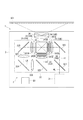
図1は、本実施形態に係るプロジェクター1の構成を示す模式図である。
プロジェクター1は、内部に設けられた光源から出射された光束を変調して画像情報に応じた画像を形成し、当該画像をスクリーンSC1等の被投射面上に拡大投射する表示装置である。
このプロジェクター1は、図1に示すように、外装筐体2と、当該外装筐体2内に収納される光学ユニット3、当該プロジェクター1を制御する制御装置CUの他、図示を省略するが、冷却対象を冷却する冷却装置、及び当該プロジェクター1を構成する電子部品に電力を供給する電源装置を備える。また、プロジェクター1は、色合成装置に入射される光の成分比率に応じて、投射光学装置から投射される画像の色域を変化させる機能を有する。
[First Embodiment]
Hereinafter, a first embodiment of the present invention will be described based on the drawings.
[Schematic configuration of projector]
FIG. 1 is a schematic diagram illustrating a configuration of a
The
As shown in FIG. 1, the
[光学ユニットの構成]
光学ユニット3は、照明装置31、色分離装置32、平行化レンズ33、複数の光変調装置34、色合成装置35、及び投射光学装置36を備える。
照明装置31は、照明光WLを出射する。なお、照明装置31の構成については、後述する。
色分離装置32は、照明装置31から入射された照明光WLを赤色光LR、緑色光LG及び青色光LBの3つの色光に分離する。この色分離装置32は、ダイクロイックミラー321,322、全反射ミラー323,324,325及びリレーレンズ326,327を備える。
[Configuration of optical unit]
The
The
The
ダイクロイックミラー321は、照明装置31からの照明光WLから青色光LB及びその他の色光(緑色光LG及び赤色光LR)を含む光を分離する。ダイクロイックミラー321は、青色光LBを透過させるとともに、緑色光LG及び赤色光LRを含む上記光を透過させる。
ダイクロイックミラー322は、ダイクロイックミラー321により分離された上記光から緑色光LG及び赤色光LRを分離する。具体的に、ダイクロイックミラー322は、緑色光LGを反射するとともに、赤色光LRを透過させる。
The
The
全反射ミラー323は、青色光LBの光路中に配置され、ダイクロイックミラー321にて透過された青色光LBを光変調装置34(34B)に向けて反射させる。一方、全反射ミラー324,325は、赤色光LRの光路中に配置され、ダイクロイックミラー322を透過した赤色光LRを光変調装置34(34R)に向けて反射させる。また、緑色光LGは、ダイクロイックミラー322にて、光変調装置34(34G)に向けて反射される。
リレーレンズ326,327は、赤色光LRの光路の、ダイクロイックミラー322の下流に配置されている。これらリレーレンズ326,327は、赤色光LRの光路長が青色光LBや緑色光LGの光路長よりも長くなることによる赤色光LRの光損失を補償する機能を有する。
The
The
平行化レンズ33は、後述する光変調装置34に入射する光を平行化する。なお、赤、緑及び青の各色光用の平行化レンズを、それぞれ33R,33G,33Bとする。また、赤、緑及び青の各色光用の光変調装置を、それぞれ34R,34G,34Bとする。
The collimating
複数の光変調装置34(34R,34G,34B)は、ダイクロイックミラー321及びダイクロイックミラー322により分離され、それぞれ入射される各色光LR,LG,LBを変調して、画像情報に応じた色画像を形成する。これら光変調装置34は、入射される光を変調する液晶パネルにより構成される。なお、光変調装置34R,34G,34Bの入射側及び出射側にはそれぞれ、入射側偏光板341(341R,341G,341B)及び出射側偏光板342(342R,342G,342B)が配置されている。
The plurality of light modulators 34 (34R, 34G, 34B) are separated by the
色合成装置35には、各光変調装置34R,34G,34Bからの画像光が入射される。この色合成装置35は、各色光LR,LG,LBに対応した画像光を合成し、この合成された画像光を投射光学装置36に向けて出射させる。本実施形態では、色合成装置35は、クロスダイクロイックプリズムにより構成される。
投射光学装置36は、色合成装置35にて合成された画像光をスクリーンSC1等の被投射面に投射する。このような構成により、スクリーンSC1に拡大された画像が投射される。
Image light from each of the
The projection
[照明装置の構成]
図2は、本実施形態のプロジェクター1における照明装置31の構成を示す概略図である。
照明装置31は、前述したように照明光WLを色分離装置32に向けて出射する。この照明装置31は、図2に示すように、光源装置4及び均一化装置5を備える。この光源装置4は、均一化装置5に向けて青色光及び蛍光を出射させ、均一化装置5は、当該入射された青色光及び蛍光を均一化し、照明光WLとして色分離装置32に向けて出射させる。
[Configuration of lighting device]
FIG. 2 is a schematic diagram illustrating a configuration of the
The
[光源装置の構成]
光源装置4は、図2に示すように、光源部41、アフォーカルレンズ42、ホモジナイザー光学系43、第1位相差板44、偏光分離装置45、第2位相差板46、第3位相差板47、蛍光反射装置6及び青色光反射装置8を備える。
光源部41は、アレイ光源411及びコリメータ光学系412を備える。このアレイ光源411は、本発明の光源に相当する複数の半導体レーザー4111により構成される。具体的に、アレイ光源411は、当該アレイ光源411から出射される光束の照明光軸Ax1に直交する一平面内に複数の半導体レーザー4111がアレイ状に配列されることにより形成される。なお、詳しくは後述するが、蛍光反射装置6にて反射された光束の照明光軸をAx2としたとき、照明光軸Ax1と照明光軸Ax2とは同一平面内にあり、且つ互いに直交している。照明光軸Ax1上においては、アレイ光源411と、コリメータ光学系412と、アフォーカルレンズ42と、ホモジナイザー光学系43と、第1位相差板44と、偏光分離装置45と、第2位相差板46と、青色光反射装置8とが、この順に並んで配置されている。
一方、照明光軸Ax2上においては、蛍光反射装置6(波長変換装置7及びピックアップ光学系61)と、偏光分離装置45と、均一化装置5(アフォーカル装置51、第1レンズアレイ52、第2レンズアレイ53及び重畳レンズ54)とが、この順に並んで配置されている。
[Configuration of light source device]
As shown in FIG. 2, the
The
On the other hand, on the illumination optical axis Ax2, the fluorescence reflection device 6 (the
アレイ光源411を構成する半導体レーザー4111は、例えば、445nmの波長領域にピーク波長を有する励起光(青色光BL)を出射する。また、半導体レーザー4111から出射される青色光BLは、s偏光及びp偏光を含むランダムな直線偏光であり、アフォーカルレンズ42に向けて出射される。そして、このアレイ光源411から出射された青色光BLは、コリメータ光学系412に入射される。
The
コリメータ光学系412は、アレイ光源411から出射された青色光BLを平行光に変換する。このコリメータ光学系412は、例えば各半導体レーザー4111に対応してアレイ状に配置された複数のコリメータレンズ4121を備える。このコリメータ光学系412を通過することにより平行光に変換された青色光BLは、アフォーカルレンズ42に入射される。
アフォーカルレンズ42は、コリメータ光学系412から入射された青色光BLの光束径を調整する。このアフォーカルレンズ42は、レンズ421と、レンズ422とを備え、青色光BLは、レンズ421により集光され、レンズ422により平行化されて、ホモジナイザー光学系43に入射する。
The collimator
The
ホモジナイザー光学系43は、被照明領域における青色光BLによる照度分布を均一化する。このホモジナイザー光学系43は、一対のマルチレンズアレイ431,432を備える。このホモジナイザー光学系43から出射された青色光BLは、第1位相差板44に入射される。
第1位相差板44は、ホモジナイザー光学系43と偏光分離装置45との間に配置され、入射される青色光BLの偏光方向を略90°回転させる。本実施形態では、第1位相差板44は、λ/2波長板により構成される。この第1位相差板44に入射された青色光BLは、偏光方向が略90°回転され、p偏光成分の青色光BLp及びs偏光成分の青色光BLsに分離され、偏光分離装置45に入射される。
The homogenizer
The
[偏光分離装置の構成]
偏光分離装置45は、いわゆるプリズム型の偏光ビームスプリッターであり、p偏光及びs偏光のうち、一方の偏光光を通過させ、他方の偏光光を反射させる。この偏光分離装置45は、プリズム451,452及び偏光分離層453を備える。これらプリズム451,452は、略三角柱形状に形成され、それぞれ照明光軸Ax1に対して45°の角度をなす傾斜面を有し、かつ、照明光軸Ax2に対して45°の角度をなしている。
[Configuration of polarization separation device]
The polarization separation device 45 is a so-called prism-type polarization beam splitter, and allows one of the p-polarized light and the s-polarized light to pass therethrough and reflects the other polarized light. The polarization separation device 45 includes
偏光分離層453は、上記傾斜面に設けられ、当該偏光分離層453に入射した青色光BLp,BLsをp偏光成分の青色光BLpとs偏光成分の青色光BLsとに分離する偏光分離機能を有する。この偏光分離層453は、s偏光成分の青色光BLsを反射させ、p偏光成分の青色光BLpを透過させる。また、偏光分離層453は、当該偏光分離層453に入射した光のうち、第1の波長帯(青色光BLs,BLpの波長帯)とは異なる第2の波長帯(蛍光YL)の光を、その偏光状態にかかわらず透過させる色分離機能を有する。なお、偏光分離装置45は、プリズム型のものに限らず、プレート型の偏光分離装置を用いてもよい。
そして、偏光分離層453に入射した青色光BLp,BLsのうち、s偏光成分の青色光BLsは、励起光BLsとして、蛍光反射装置6に向けて反射される。
The polarization separation layer 453 is provided on the inclined surface, and has a polarization separation function for separating the blue light BLp and BLs incident on the polarization separation layer 453 into the p-polarized component blue light BLp and the s-polarized component blue light BLs. Have. The polarization separation layer 453 reflects the blue light BLs of the s-polarized component and transmits the blue light BLp of the p-polarized component. Further, the polarization separation layer 453 emits light in a second wavelength band (fluorescence YL) different from the first wavelength band (blue light BLs, BLp wavelength band) out of the light incident on the polarization separation layer 453. The color separation function allows transmission regardless of the polarization state. The polarization separation device 45 is not limited to a prism type, and a plate type polarization separation device may be used.
Of the blue light BLp and BLs incident on the polarization separation layer 453, the blue light BLs of the s-polarized component is reflected toward the
[蛍光反射装置の構成]
蛍光反射装置6は、偏光分離装置45から入射されたs偏光成分の青色光(励起光)BLsを蛍光YLに変換し、当該偏光分離装置45に向けて反射させる。この蛍光反射装置6は、ピックアップ光学系61及び波長変換装置7を備える。これらのうち、ピックアップ光学系61は、励起光BLsを波長変換装置7の波長変換層72に向けて集光させる。このピックアップ光学系61は、レンズ611、レンズ612及びレンズ613を備える。具体的に、ピックアップ光学系61は、入射された複数の光束(励起光BLs)を後述する波長変換層72に向けて集光させるとともに、当該波長変換層72上で互いに重畳させる。
この波長変換層72により青色光BLsは、蛍光YLに変換され、再度ピックアップ光学系61に入射され、当該ピックアップ光学系61を介して偏光分離装置45に入射される。
なお、波長変換装置7の構成については、後述する。
[Configuration of Fluorescent Reflector]
The
The blue light BLs is converted into fluorescence YL by the
The configuration of the
一方、偏光分離層453に入射した青色光BLp,BLsのうち、p偏光成分の青色光BLpは、当該偏光分離層453を透過し、第2位相差板46に入射される。
第2位相差板46は、青色光反射装置8と偏光分離装置45との間に配置され、入射されるp偏光成分の青色光BLpを円偏光に変換させる。本実施形態では、この第2位相差板46は、λ/4波長板により構成される。そして、第2位相差板46により円偏光に変換された青色光BLpは、青色光反射装置8に入射される。
On the other hand, of the blue light BLp and BLs incident on the polarization separation layer 453, the blue light BLp of the p-polarized component is transmitted through the polarization separation layer 453 and incident on the
The
[青色光反射装置の構成]
青色光反射装置8は、偏光分離装置45から入射されたp偏光成分の青色光BLpを拡散させて、当該偏光分離装置45に向けて反射させる。この青色光反射装置8は、ピックアップ光学系81と、拡散反射装置82とを備える。これらのうち、ピックアップ光学系81は、励起光BLpを拡散反射装置82の拡散反射層822に向けて集光させる。このピックアップ光学系81は、レンズ811、レンズ812及びレンズ813を備える。具体的に、ピックアップ光学系81は、入射された複数の光束(励起光BLp)を後述する拡散反射層822に向けて集光させるとともに、当該拡散反射層822上で互いに重畳させる。
[Configuration of Blue Light Reflector]
The blue light reflection device 8 diffuses the p-polarized component blue light BLp incident from the polarization separation device 45 and reflects it toward the polarization separation device 45. The blue light reflection device 8 includes a pickup
拡散反射装置82は、入射された青色光BLpを拡散させて反射させる機能を有する。この拡散反射装置82は、基材821、拡散反射層822及びモーター823を備える。基材821は、略円板状の基材により構成され、当該基材821のピックアップ光学系81側の面には、拡散反射層822が形成されている。この拡散反射層822は、入射された光を散乱させて反射させる機能を有する。
モーター823は、基材821の上記拡散反射層822が設けられた側とは反対方向側に取り付けられ、当該モーター823の駆動により基材821が回転する。これにより、拡散反射層822が冷却される。
このような構成により、拡散反射装置82に入射された青色光BLpは、拡散反射層822に入射され、当該拡散反射層822により拡散(散乱)され、ピックアップ光学系81に向けて出射される。そして、上記青色光BLpは、ピックアップ光学系81により集光されて、第2位相差板46に再度入射される。これにより、青色光BLpは、拡散反射層822により回転方向が反転されて、第2位相差板46に入射され、偏光方向が円偏光から直線偏光に変換される。このため、拡散反射層822により反射された青色光BLpは、s偏光成分の青色光BLsとして出射される。そして、青色光BLsは、偏光分離装置45に入射される。
The diffuse
The
With such a configuration, the blue light BLp incident on the diffuse
拡散反射装置82及びピックアップ光学系81を介して偏光分離装置45に入射された青色光BLsは、偏光分離層453に反射され、当該偏光分離装置45のプリズム452側から出射され、第3位相差板47に入射される。
一方、偏光分離装置45に入射された蛍光YLは、偏光分離層453を介して、当該偏光分離装置45のプリズム452側から出射され、上記第3位相差板47に入射される。
第3位相差板47は、偏光分離装置45と均一化装置5との間に配置され、入射される青色光BLs及び蛍光YLの偏光方向を略90°回転させる。本実施形態では、第3位相差板47は、λ/2波長板により構成される。この第3位相差板47に入射された青色光BLsは、偏光方向が略90°回転され、p偏光成分の青色光BLpとして、均一化装置5に向けて出射される。また、蛍光YLは、励起光BLsに基づく光であるため、s偏光成分の光である。このため、第3位相差板47に入射された蛍光YLは、p偏光成分の蛍光YLとして、均一化装置5に向けて出射される。
The blue light BLs incident on the polarization separation device 45 via the diffuse
On the other hand, the fluorescence YL incident on the polarization separation device 45 is emitted from the
The third
[均一化装置の構成]
均一化装置5は、光源装置4から出射された青色光BL及び蛍光YLを均一化する機能を有する。この均一化装置5は、図2に示すように、アフォーカル装置51、第1レンズアレイ52、第2レンズアレイ53及び重畳レンズ54を備える。
これらのうち、アフォーカル装置51は、光源装置4から入射された蛍光YL及び青色光BLのビーム系を拡大する機能を有する。具体的に、このアフォーカル装置51は、光源装置4を介して入射された蛍光YL及び青色光BLに基づいて、第2レンズアレイ53の第2レンズ531上に表示される光源像の大きさを調整する。
このアフォーカル装置51は、凹レンズ511及び凸レンズ512からなるアフォーカルレンズにより構成される。凹レンズ511は、入射された蛍光YL及び青色光BLを拡散させ、凸レンズ512に向けて出射させる。凸レンズ512は、凹レンズ511から拡散されて入射された蛍光YL及び青色光BLを平行化して第1レンズアレイ52に向けて出射させる。
[Configuration of homogenizer]
The
Among these, the
The
第1レンズアレイ52は、アフォーカル装置51から出射された光(光束)の中心軸(上記照明光軸Ax2)に対する直交面内にアレイ状に配列された複数の第1レンズ521を有する。この第1レンズアレイ52は、第1レンズアレイ52の複数の第1レンズ521により、当該第1レンズアレイ52に入射された光束を複数の部分光束に分割する。
第2レンズアレイ53は、上記照明光軸Ax1に対する直交面内にアレイ状に配列された第1レンズアレイ52の複数の第1レンズ521に応じた複数の第2レンズ531を有する。この第2レンズアレイ53は、複数の第2レンズ531により、第1レンズ521により分割された部分光束を被照明領域としての重畳レンズ54に重畳させる。
The
The
重畳レンズ54は、照明光WLを被照明領域において重畳させることにより、被照明領域の照度分布を均一化する。このようにして、蛍光YL及び青色光BLは、重畳レンズ54により合成され、照度分布が均一化された照明光WLとして、照明装置31からダイクロイックミラー321に向けて出射される。
The superimposing
[波長変換装置の構成]
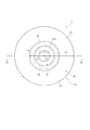
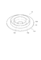
図3は、波長変換装置7を偏光分離装置45側から見た平面図である。
波長変換装置7は、図2及び図3に示すように、基材71及びモーター75を備える。
基材71は、略円板状に形成されている。この基材71は、当該基材71の偏光分離装置45側(ピックアップ光学系61)の第1面711と、当該第1面711に対向する第2面712と、を有する。また、基材71の略中央部分には、開口部713が形成されている。この開口部713には、モーター75の一部が嵌め込まれる。なお、上記基材71は、アルミニウムにより構成され、当該基材71の厚さ寸法は、略1mmに設定されている。
また、上記第1面711及び第2面712のうち、ピックアップ光学系61に対向する面である第1面711には、波長変換層72が配置されている。
[Configuration of wavelength converter]
FIG. 3 is a plan view of the
As shown in FIGS. 2 and 3, the
The
A
波長変換層72は、本発明の波長変換部に相当し、上述したように基材71の第1面711に配置される。具体的に、波長変換層72は、例えば、マスク印刷法により環状に印刷され、基材71の開口部713の外側に形成される。この波長変換層72は、例えば、YAG蛍光体を含む波長変換素子であり、当該波長変換層72に入射された青色光BLsを蛍光YLに変換する。
また、基材71は、当該基材71を光入射側から見た場合に、波長変換層72より内側に位置する第1領域73と、当該波長変換層72より外側に位置する領域である第2領域74を有する。これらのうち、第2領域74の表面積は、第1領域73の表面積より大きく設定されている。
なお、図2及び図3においては、図示を省略するが、当該波長変換層72と基材71との間には、反射層が形成されている。
The
The
Although not shown in FIGS. 2 and 3, a reflective layer is formed between the
[第1領域の面積と第2領域の面積]
ここで、開口部713の半径とは、例えば、図3における回転軸Pから開口部713の外周縁までの距離L1であり、基材71の外径とは、例えば、図3における回転軸Pから基材71の外周縁までの距離L2であり、波長変換層72の内径とは、例えば、図3における回転軸Pから波長変換層72の内周縁までの距離L3であり、波長変換層72の外径とは、例えば、図3における回転軸Pから波長変換層72の外周縁までの距離L4である。なお、回転軸Pは、基材71の中心と一致している。
本実施形態では、上記距離L1は略10mm、上記距離L2は略55mm、上記距離L3は略20mm、上記距離L4は略31.5mmに設定されている。このため、基材71の第1面711において、第2領域74の表面積は、第1領域73の表面積より大きい。
[Area of first region and area of second region]
Here, the radius of the
In this embodiment, the distance L1 is set to about 10 mm, the distance L2 is set to about 55 mm, the distance L3 is set to about 20 mm, and the distance L4 is set to about 31.5 mm. For this reason, on the
本発明の回転装置は、モーター75により構成され、回転軸Pを中心に基材71を回転させる機能を有する。具体的に、モーター75の一部は、基材71の開口部713に嵌めこまれ、当該モーター75の駆動により基材71が回転する。これにより、ピックアップ光学系61から出射された青色光BLsは、回転状態の基材71における波長変換層72に入射され、蛍光YLに変換されて上記反射層により反射される。
The rotating device of the present invention is constituted by a
[基材の外径と波長変換層の温度との関係]
図4は、基材の外径と波長変換層の温度との関係を示す図である。
なお、図4の説明においては、入射されるレーザー光の光量は一定であり、上記距離L1は略10mmであり、上記距離L3は略20mmであり、上記距離L4は略31.5mmであるものとする。また、基材の厚さ寸法は、略1mmであり、当該基材は、アルミニウムにより構成されているものとし、上記基材の外径(距離L2)のみ変化した場合について説明する。
[Relationship between outer diameter of substrate and temperature of wavelength conversion layer]
FIG. 4 is a diagram showing the relationship between the outer diameter of the substrate and the temperature of the wavelength conversion layer.
In the description of FIG. 4, the amount of incident laser light is constant, the distance L1 is approximately 10 mm, the distance L3 is approximately 20 mm, and the distance L4 is approximately 31.5 mm. And Moreover, the thickness dimension of a base material is about 1 mm, the said base material shall be comprised with aluminum, and the case where only the outer diameter (distance L2) of the said base material changes is demonstrated.
基材の外径が変化すると、蛍光体の温度は、図4に示す線S1に示すように変化する。すなわち、基材の外径(距離L2)が大きくなるに従い、蛍光体の温度が低くなる。具体的に、基材の外径(距離L2)が50mmの場合、図4に示すように、蛍光体の温度は、最大略370℃まで上昇する。これに対し、上記距離L2が80mmの場合、蛍光体の温度は、最大略200℃まで上昇する。更に、上記距離L2が120mmの場合、蛍光体の温度は、最大略160℃まで上昇する。すなわち、上記基材の外径(距離L2)が大きくなるにつれて、波長変換層72の温度が上昇することを抑制できる。
When the outer diameter of the substrate changes, the temperature of the phosphor changes as shown by a line S1 shown in FIG. That is, as the outer diameter (distance L2) of the substrate increases, the temperature of the phosphor decreases. Specifically, when the outer diameter (distance L2) of the substrate is 50 mm, the temperature of the phosphor rises to a maximum of approximately 370 ° C. as shown in FIG. On the other hand, when the distance L2 is 80 mm, the temperature of the phosphor rises to about 200 ° C. at the maximum. Furthermore, when the distance L2 is 120 mm, the temperature of the phosphor rises to a maximum of approximately 160 ° C. That is, the temperature of the
すなわち、第1領域73の表面積に対して、第2領域74の表面積が大きくなるにつれて、蛍光体の温度が上昇することをより抑制できる。
That is, as the surface area of the
[第1実施形態の効果]
本発明の第1実施形態に係るプロジェクター1によれば、以下の効果がある。
モーター75により回転する基材71の第1面711に波長変換層72が環状に配置され、当該波長変換層72より内側に位置する第1領域73の表面積より、当該波長変換層72より外側に位置する第2領域74の表面積が大きい。このため、波長変換層72に光が入射され、当該波長変換層72の熱が上昇すると、第1領域73は、表面積が限られているので、熱飽和する可能性が高い。これに対し、第2領域74は、波長変換層72より外側に位置するので、設計により第2領域74の表面積を第1領域73の表面積より拡大すれば、熱飽和を生じにくくできる。これによれば、波長変換層72にて生じた熱を当該波長変換層72より内側の第1領域73及び外側の第2領域74に伝導できるので、波長変換層72を効率よく冷却できる。従って、波長変換装置7の波長変換効率の低下を抑制できる。
[Effect of the first embodiment]
The
The
波長変換装置7の波長変換効率の低下を抑制できるので、波長変換層72によって生じる蛍光光の光量の低下を抑制でき、光源部41からの光の利用効率を向上させることができる。従って、上記波長変換装置7を備えた照明装置31は、信頼性が高く、温度影響を受けない安定した拡散特性及び位相差特性を得ることができるので、当該照明装置31、ひいてはプロジェクター1の信頼性及び安定性を高くできる。
Since a decrease in the wavelength conversion efficiency of the
[第2実施形態]
次に、本発明の第2実施形態について説明する。
本実施形態に係るプロジェクターは、上記第1実施形態に係るプロジェクター1と略同一の構成を備える他、上記プロジェクター1と波長変換装置の基材の形状が一部異なる。具体的に、上記プロジェクター1の波長変換装置7は、基材71を備えるのに対し、本実施形態の波長変換装置は、複数の凸部を有する基材を備えている点で相違する。
なお、以下の説明では、既に説明した部分と同一又は略同一である部分については、同様の符号を付して説明を省略する。
[Second Embodiment]
Next, a second embodiment of the present invention will be described.
The projector according to the present embodiment has substantially the same configuration as the
In the following description, parts that are the same as or substantially the same as those already described are given the same reference numerals and description thereof is omitted.
図5は、本実施形態に係るプロジェクターの波長変換装置を示す断面図である。
波長変換装置7Aは、図6に示すように、基材71A、波長変換層72、及びモーター75を備える。
基材71Aは、略円板状に形成され、当該基材71Aにおける第1面711Aの波長変換層72より外側の領域には、直線状に延びる複数の凸部71A1が形成されている。この複数の凸部71A1は、波長変換層72より外側に位置する第2領域74Aに一定間隔を持って配置される。このため、基材71Aにおける第2領域74Aには、複数の凹凸が形成される。なお、複数の凸部71A1は、例えば、基材71Aに対してプレス加工を行うことにより形成される。
FIG. 5 is a cross-sectional view showing the wavelength converter of the projector according to the present embodiment.
As illustrated in FIG. 6, the
The
また、本実施形態においても、上記距離L1〜L4は、上記第1実施形態と同一であるため、第2領域74Aの表面積は、上記凹凸が形成されることにより、第1実施形態の第2領域74の表面積より大きくなる。従って、基材71Aの第1面711Aにおいて、第2領域74Aの面積は、第1領域73Aの面積より確実に大きくなる。
Also in the present embodiment, the distances L1 to L4 are the same as those in the first embodiment, so that the surface area of the
[第2実施形態の効果]
本実施形態に係るプロジェクターは、上記第1実施形態に係るプロジェクター1と同様の効果を奏する他、以下の効果を奏する。
基材71Aの第1面711Aにおける波長変換層72より外側の領域(第2領域74A)が複数の凹凸を有しているので、当該第2領域が平坦状である場合に比べて、当該第2領域74Aの表面積、すなわち、波長変換層72の熱を放熱する放熱面積を拡大できる。従って、波長変換装置7Aの波長変換効率の低下をより抑制できる。
[Effects of Second Embodiment]
The projector according to this embodiment has the following effects in addition to the same effects as the
Since the region (
[第2実施形態の変形例]
上記第2実施形態の波長変換装置7Aは、基材71Aを備え、当該基材71Aの第1面711Aの波長変換層72より外側の第2領域74Aには、複数の凸部71A1が形成されていることとした。しかしながら、本発明は、これに限らない。
[Modification of Second Embodiment]
The
図6は、本実施形態の変形例に係る波長変換装置7Bの基材71Bの斜視図である。
波長変換装置7Bは、基材71Aに代えて基材71Bを備える。この基材71Bの第1面711Bにおける波長変換層72より外側に位置する第2領域74Bには、複数の凹部71B1と複数の凸部71B2がそれぞれ形成されている。これら複数の凹部71B1及び複数の凸部71B2は、それぞれ凹部71B1と凸部71B2とが隣り合うように、第1面711Bに形成される。なお、複数の凹部71B1及び凸部71B2は、基材71Bに対して、例えば、プレス加工を行うことにより形成される。
FIG. 6 is a perspective view of the
The
また、本変形例においても、上記距離L1〜L4は、上記第2実施形態と同一であるため、第2領域74Bの表面積は、複数の凹部71B1及び複数の凸部71B2が形成されることにより、上記第1実施形態の第2領域74の表面積より大きくなる。従って、基材71Bの第1面711Bにおいて、第2領域74Bの面積は、第1領域73Bの面積より確実に大きくなる。従って、上記第2実施形態と同様の作用効果を奏することができる。
また、本変形例では、第2領域74Bに複数の凹部71B1及び複数の凸部71B2が形成されているので、モーター75の駆動により基材71Bが回転すると、冷却気体が回転軸Pから当該波長変換層72の外側に流通する際に、複数の凹部71B1及び複数の凸部71B2により気流が乱され、乱流や渦流が発生する。これにより、基材71Bの第2領域74Bを冷却気体により効率よく冷却できる。従って、波長変換装置7Bの波長変換効率の低下をより抑制できる。
Also in the present modification, the distances L1 to L4 are the same as those in the second embodiment, so that the surface area of the
In the present modification, since the plurality of concave portions 71B1 and the plurality of convex portions 71B2 are formed in the
[第3実施形態]
次に、本発明の第3実施形態について説明する。
本実施形態に係るプロジェクターは、上記第1実施形態に係るプロジェクター1と略同一の構成を備える他、上記プロジェクター1と波長変換装置の基材の形状が一部異なる。具体的に、上記プロジェクター1の波長変換装置7は、基材71を備えるのに対し、本実施形態の波長変換装置は、貫通孔が形成された基材を備えている点で相違する。
なお、以下の説明では、既に説明した部分と同一又は略同一である部分については、同様の符号を付して説明を省略する。
[Third Embodiment]
Next, a third embodiment of the present invention will be described.
The projector according to the present embodiment has substantially the same configuration as the
In the following description, parts that are the same as or substantially the same as those already described are given the same reference numerals and description thereof is omitted.
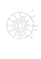
図7は、本実施形態に係るプロジェクターの波長変換装置7Cを示す平面図である。
波長変換装置7Cは、図8に示すように、基材71C、波長変換層72、及びモーター75を備える。
基材71Cは、略円板状に形成され、当該基材71Cにおける第1面711Cの波長変換層72の外側に位置する第2領域74Cには、複数の貫通孔71C1が形成されている。この複数の貫通孔71C1は、波長変換層72の外側に位置する第2領域74Cに一定間隔を持って放射状に配置される。なお、複数の貫通孔71C1は、基材71Cに対して、例えば、プレス加工を行うことにより形成される。
FIG. 7 is a plan view showing a wavelength conversion device 7C of the projector according to the present embodiment.
As illustrated in FIG. 8, the
The base material 71C is formed in a substantially disc shape, and a plurality of through holes 71C1 are formed in the
また、本実施形態においても、上記距離L1〜L4は、上記第1実施形態と同一であるため、第2領域74Cの表面積は、上記複数の貫通孔71C1が形成されることにより、第1実施形態の第2領域74の表面積より大きくなる。従って、基材71Cの第1面711Cにおいて、第2領域74Cの面積は、第1領域73Cの面積より確実に大きくなる。
更に、本実施形態では、第2領域74Cに複数の貫通孔71C1が形成されているので、モーター75の駆動により基材71Cが回転すると、冷却気体が回転軸Pから当該波長変換層72の外側に流通する際に、複数の貫通孔71C1を流通する。
Also in the present embodiment, the distances L1 to L4 are the same as those in the first embodiment. Therefore, the surface area of the
Further, in the present embodiment, since the plurality of through holes 71C1 are formed in the
[第3実施形態の効果]
本実施形態に係るプロジェクターは、上記第1実施形態に係るプロジェクター1と同様の効果を奏する他、以下の効果を奏する。
基材71Cにおける波長変換層72より外側に位置する第2領域74Cに当該基材71Cを貫通する複数の貫通孔71C1が複数形成されているので、当該第2領域が平坦状である場合に比べて、第2領域C1の上記放熱面積を拡大できる。従って波長変換装置7Cの波長変換効率の低下を更に抑制できる。
[Effect of the third embodiment]
The projector according to this embodiment has the following effects in addition to the same effects as the
Since a plurality of through holes 71C1 penetrating the base material 71C are formed in the
[第4実施形態]
次に、本発明の第4実施形態について説明する。
本実施形態に係るプロジェクターは、上記第1実施形態に係るプロジェクター1と略同一の構成を備える他、上記プロジェクター1と波長変換装置の基材の形状が一部異なる。具体的に、上記プロジェクター1の波長変換装置7は、基材71を備えるのに対し、本実施形態の波長変換装置は、複数の突出部を備えた基材を備えている点で相違する。
なお、以下の説明では、既に説明した部分と同一又は略同一である部分については、同様の符号を付して説明を省略する。
[Fourth Embodiment]
Next, a fourth embodiment of the present invention will be described.
The projector according to the present embodiment has substantially the same configuration as the
In the following description, parts that are the same as or substantially the same as those already described are given the same reference numerals and description thereof is omitted.
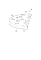
図8は、本実施形態に係るプロジェクターの波長変換装置7Dを光の入射方向とは反対方向側から見た斜視図であり、図9は、本実施形態に係る波長変換装置7Dの断面図である。なお、図8では、モーター75の図示を省略している。
波長変換装置7Dは、図8及び図9に示すように、基材71D、波長変換層72、及びモーター75を備える。
基材71Dは、略円板状に形成され、第1面711D及び第1面711Dに対向する第2面712Dを有する。これらのうち、基材71Dの第2面712Dには、当該第2面712Dの法線方向に延びる第1突出部71D1及び第2突出部71D2を備える。
第1突出部71D1は、環状に形成され、第2面712Dにおいて、第1面711D側の波長変換層72に対向する位置に配置される。また、第2突出部71D2は、第1突出部71D1と同様に環状に形成され、第1突出部71D1の外側に配置される。また、これら第1突出部71D1及び第2突出部71D2の第2面712Dから突出する高さは略同一に設定されている。
FIG. 8 is a perspective view of the
As shown in FIGS. 8 and 9, the
The
The first protrusion 71D1 is formed in an annular shape, and is disposed on the
本実施形態においても、上記距離L1〜L4は、上記第1実施形態と同一であるため、第2領域74Dの表面積は、上記第2突出部71D2が形成されることにより、第1実施形態の第2領域74の表面積より大きくなる。従って、第2領域74Dの表面積は、第1領域73Dの面積より確実に大きくなる。
更に、本実施形態では、第1突出部71D1及び第2突出部71D2が形成されているので、モーター75の駆動により基材71Dが回転すると、冷却気体が回転軸Pから当該波長変換層72の外側に流通する際に、第1突出部71D1及び第2突出部71D2に流通する。
Also in this embodiment, since the distances L1 to L4 are the same as those in the first embodiment, the surface area of the
Furthermore, in this embodiment, since the first protrusion 71D1 and the second protrusion 71D2 are formed, when the
[第4実施形態の効果]
本実施形態に係るプロジェクターは、上記第1実施形態に係るプロジェクター1と同様の効果を奏する他、以下の効果を奏する。
基材71Dの第2面712Dから当該第2面712Dの法線方向に突出する第1突出部71D1及び第2突出部71D2を有するので、当該第2領域に突出部を設けられていない場合に比べて、第2領域74Dの上記放熱面積を拡大できる。従って、波長変換装置7Dの波長変換効率の低下を確実に抑制できる。
[Effect of Fourth Embodiment]
The projector according to this embodiment has the following effects in addition to the same effects as the
Since it has 1st protrusion part 71D1 and 2nd protrusion part 71D2 which protrude in the normal line direction of the said
また、第2面712Dにおける波長変換層72に対向する位置に第1突出部71D1が形成されているので、第1突出部71D1に波長変換層72からの熱が伝導され、当該第1突出部71D1に冷却気体が流通することで、波長変換層72をより効率よく冷却できる。
Further, since the first protrusion 71D1 is formed at a position facing the
[第5実施形態]
次に、本発明の第5実施形態について説明する。
本実施形態に係るプロジェクターは、上記第1実施形態に係るプロジェクター1と略同一の構成を備える他、上記プロジェクター1と波長変換装置の基材の形状が一部異なる。具体的に、上記プロジェクター1の波長変換装置7は、円板状の基材71を備えるのに対し、本実施形態の波長変換装置は、円筒状の基材を備えている点で相違する。
なお、以下の説明では、既に説明した部分と同一又は略同一である部分については、同様の符号を付して説明を省略する。
[Fifth Embodiment]
Next, a fifth embodiment of the present invention will be described.
The projector according to the present embodiment has substantially the same configuration as the
In the following description, parts that are the same as or substantially the same as those already described are given the same reference numerals and description thereof is omitted.
図10は、本実施形態に係るプロジェクターの波長変換装置7Eを示す斜視図である。なお、図10では、モーター75の図示を省略している。
波長変換装置7Eの基材71Eは、略円筒状に形成され、略円板状の平板部71E1と、当該平板部71E1の外周縁から第2面712Eの法線方向に延びる円環部71E2を備える。これらのうち、平板部71E1は、第1面711E及び第1面711Eに対向する第2面712Eを有する。また、平板部71E1の略中央には、上記開口部713が形成され、第1面711Eにおける当該開口部713を囲む位置に、波長変換層72が形成されている。
また、円環部71E2は、本発明の突出部に相当し、第2面712Eにおける平板部71E1の外周縁から、当該第2面712Eの法線方向に延びる円環状に形成されている。この円環部71E2の厚さ寸法(距離L5)は、略5mmに設定されている。更に、円環部71E2の高さ寸法(距離L6)は、略35mmに設定されている。すなわち、回転軸Pから波長変換層72の外縁までの距離L3と上記距離L5及び上記距離L6の和が上記距離L2より略5mm大きく設定されている。
なお、本実施形態では、円環部71E2と、第1面711Eにおける第1領域73E及び波長変換層72以外の領域(波長変換層72より外側の領域)と、が本実施形態における第2領域74Eとなる。
FIG. 10 is a perspective view showing a
The
The annular portion 71E2 corresponds to a protruding portion of the present invention, and is formed in an annular shape extending from the outer peripheral edge of the flat plate portion 71E1 on the
In the present embodiment, the annular portion 71E2 and the region other than the
本実施形態においても、上記距離L1,L3,L4は、上記第1実施形態と同一であり、回転軸Pから波長変換層72の外縁までの距離L3と上記距離L5及び上記距離L6の和が上記距離L2より大きくに設定されているので、第2領域74Eの表面積は、上記円環部71E2が形成されることにより、第1実施形態の第2領域74の表面積より大きくなる。従って、基材71Eにおいて、第2領域74Eの面積は、第1領域73Eの面積より確実に大きくなる。
また、本実施形態では、円環部71E2が形成されているので、モーター75の駆動により基材71Eが回転すると、冷却気体が回転軸Pから当該波長変換層72の外側に流通する際に、円環部71E2に流通する。
更に、本実施形態では、平板部71E1の半径(上記距離L3と上記L5との和)が第1実施形態の基材71の半径(上記距離L2)より小さくなる。
Also in this embodiment, the distances L1, L3, and L4 are the same as those in the first embodiment, and the sum of the distance L3 from the rotation axis P to the outer edge of the
In the present embodiment, since the annular portion 71E2 is formed, when the
Further, in the present embodiment, the radius of the flat plate portion 71E1 (the sum of the distance L3 and L5) is smaller than the radius of the base material 71 (the distance L2) of the first embodiment.
[第5実施形態の効果]
本実施形態に係るプロジェクターは、上記第4実施形態に係るプロジェクター1と同様の効果を奏する他、以下の効果を奏する。
平板部71E1の半径(上記距離L3と上記L5との和)が第1実施形態の基材71の半径(上記距離L2)より小さくできるので、波長変換装置7Eを小型化できる。また、波長変換装置7Eを小型化できることから、当該波長変換装置7Eを備える照明装置、ひいてはプロジェクターを小型化できる。
[Effect of Fifth Embodiment]
The projector according to the present embodiment has the following effects in addition to the same effects as the
Since the radius (the sum of the distance L3 and the L5) of the flat plate portion 71E1 can be smaller than the radius (the distance L2) of the
[実施形態の変形]
本発明は、上記各実施形態に限定されるものではなく、本発明の目的を達成できる範囲での変形、改良等は本発明に含まれるものである。
上記各実施形態では、基材71,71A〜71Eは、アルミニウムにより構成されていることとした。しかしながら、本発明は、これに限らない。例えば、透過型の波長変換装置であれば、当該基材は、ガラス等の透光性部材により構成されることとすればよい。
上記第1〜第4実施形態では、上記距離L1は略10mmであり、上記距離L2は略55mmであり、上記距離L3は略20mmであり、上記距離L4は略31.5mmであることとした。しかしながら、本発明は、これに限らない。すなわち、第1領域73,73A〜73Eの表面積より第2領域74,74A〜74Eの表面積が大きくなれば、上記距離L1〜L4は、如何なる値に設定されてもよい。
[Modification of Embodiment]
The present invention is not limited to the above-described embodiments, and modifications, improvements, and the like within the scope that can achieve the object of the present invention are included in the present invention.
In the above embodiments, the
In the first to fourth embodiments, the distance L1 is approximately 10 mm, the distance L2 is approximately 55 mm, the distance L3 is approximately 20 mm, and the distance L4 is approximately 31.5 mm. . However, the present invention is not limited to this. That is, the distances L1 to L4 may be set to any value as long as the surface areas of the
上記各実施形態では、波長変換層72は、円環状に形成されることとした。しかしながら、本発明は、これに限らない。例えば、円弧状の波長変換層が一定の間隔を持って円環状に配置される構成であってもよい。すなわち、波長変換層の内側である第1領域73,73A〜73E、及び波長変換層の外側である第2領域74,74A〜74Eを区画できる形状であればよい。
In the above embodiments, the
上記第1実施形態では、波長変換層72は、マスク印刷法により基材71に形成されることとした。しかしながら、本発明は、これに限らない。例えば、予め成形された波長変換層72を基材71に接着することとしてもよい。
上記第2〜第4実施形態では、複数の凸部71A1、複数の凹部71B1及び凸部71B2、複数の貫通孔71C1は、基材71A,71B,71Cに対してプレス加工を行うことにより形成されることとした。しかしながら、本発明は、これに限らない。例えば、複数の凸部71A1、複数の凹部71B1及び凸部71B2、複数の貫通孔71C1は、基材71A〜71Cに対してブラスト加工やエッジングにより形成されることとしてもよい。
In the first embodiment, the
In the second to fourth embodiments, the plurality of convex portions 71A1, the plurality of concave portions 71B1 and the convex portions 71B2, and the plurality of through holes 71C1 are formed by pressing the
上記第2実施形態では、複数の凸部71A1を第2領域74Aの第1面711Aに設けることとした。しかしながら、本発明は、これに限らない。例えば、複数の凸部71A1を第2面712Aに更に設けることとしてもよいし、第2面712Aにのみ設けることとしてもよい。この場合であっても、上記第2実施形態と同様の効果を奏することができる。また、上記第2実施形態の変形例においても同様である。
In the second embodiment, the plurality of convex portions 71A1 are provided on the
上記第3実施形態では、複数の貫通孔71C1は、波長変換層72より外側に位置する第2領域74Cに一定間隔を持って放射状に配置されることとした。しかしながら、本発明は、これに限らない。例えば、波長変換層72より外側に位置する第2領域74Cの全領域に一定の間隔を持って配置されるようにしてもよいし、円弧状の貫通孔を複数放射状に配置されるようにしてもよい。すなわち、基材71Cの第2領域74Cに複数の貫通孔が形成されていればよい。
In the third embodiment, the plurality of through
上記第4実施形態では、第1突出部71D1及び第2突出部71D2の第2面712Dから突出する高さは略同一に設定されることとしたが、これに限られず、第1突出部71D1及び第2突出部71D2のいずれかの突出部が他方の突出より更に突出していてもよい。また、第1突出部71D1及び第2突出部71D2を備えることとしたが、いずれか1つの突出部のみを設けるようにしてもよいし、第1突出部71D1の内側及び第2突出部71D2の外側の少なくとも一方に環状の突出部を更に設けるようにしてもよい。すなわち、基材71Dの第2面712Dに突出部が形成されていればよい。
In the fourth embodiment, the height of the first projecting portion 71D1 and the second projecting portion 71D2 projecting from the
また、上記第4実施形態では、第1突出部71D1及び第2突出部71D2は、基材71Dの第2面712Dに形成されていた。しかしながら、本発明は、これに限らない。例えば、第1突出部71D1及び第2突出部71D2が第1面711Dに形成されていてもよいし、第1突出部71D1及び第2突出部71D2の一方が第1面711Dに形成され、他方が第2面712Dに形成されていてもよい。
Moreover, in the said 4th Embodiment, 1st protrusion part 71D1 and 2nd protrusion part 71D2 were formed in
上記第5実施形態では、円環部71E2は、第2面712Eの法線方向に突出する形状であることとした。しかしながら、本発明は、これに限らない。例えば、円環部71E2は、第2面712Eから上記法線に対して傾斜する方向に突出することとしてもよいし、第1面711Eの法線方向に突出することとしてもよい。この場合であっても、上記第5実施形態と同様の効果を奏することができる。
In the fifth embodiment, the annular portion 71E2 has a shape protruding in the normal direction of the
上記第2〜第5実施形態では、複数の凸部71A1、複数の凹部71B1及び凸部71B2、複数の貫通孔71C1、第1突出部71D1及び第2突出部71D2、並びに、円環部71E2をそれぞれ備えることとした。しかしながら、本発明は、これに限らない。例えば、基材71に複数の凸部71A1及び複数の貫通孔71C1を備えることとしてもよいし、複数の貫通孔71C1、第1突出部71D1及び第2突出部71D2を備えることとしてもよいし、複数の凸部71A1及び円環部71E2を備えることとしてもよい。すなわち、これら複数の凸部71A1、複数の凹部71B1及び凸部71B2、複数の貫通孔71C1、第1突出部71D1及び第2突出部71D2、並びに、円環部71E2をどのように組み合わせて基材に形成してもよい。換言すると、第1領域73の表面積より、第2領域74の表面積が大きければ、基材はどのような形状であってもよい。
In the second to fifth embodiments, the plurality of convex portions 71A1, the plurality of concave portions 71B1 and the convex portions 71B2, the plurality of through holes 71C1, the first projecting portion 71D1, the second projecting portion 71D2, and the annular portion 71E2 are provided. We decided to prepare each. However, the present invention is not limited to this. For example, the
上記各実施形態では、光変調装置として透過型の光変調装置を用いることとした。しかしながら、本発明は、これに限らない。例えば、光変調装置として反射型の光変調装置を用いてもよい。この場合、色分離装置32を設けることなく、当該色合成装置35により、色分離及び色合成を実行するようにしてもよい。
In each of the above embodiments, a transmissive light modulation device is used as the light modulation device. However, the present invention is not limited to this. For example, a reflection type light modulation device may be used as the light modulation device. In this case, color separation and color synthesis may be executed by the
上記各実施形態では、プロジェクター1は、3つの光変調装置34(34R,34G,34B)を備えるとしたが、本発明はこれに限らない。例えば、光変調装置は、1つでもよいし、2つでもよいし、4つ以上でもよい。
また、光変調装置として、デジタルマイクロミラーデバイス等、液晶パネル以外の光変調装置を用いてもよい。
In each of the above embodiments, the
Further, as the light modulation device, a light modulation device other than the liquid crystal panel such as a digital micromirror device may be used.
1…プロジェクター、31…照明装置、34…光変調装置、36…投射光学装置、4111…半導体レーザー(光源)、7,7A,7B,7C,7D,7E…波長変換装置、71,71A,71B,71C,71D,71E…基材、711,711A,711B,711C,711D,711E…第1面、712,712A,712D,712E…第2面、713…開口部、71A1…凸部、71B1…凹部、71B2…凸部、71C1…貫通孔、71D1…第1突出部(突出部)、71D2…第2突出部(突出部)、71E2…円環部(突出部)、72…波長変換層(波長変換部)、75…モーター(回転装置)、73,73A,73B,73C,73D,73E…第1領域、74,74A,74B,74C,74D,74E…第2領域、L1…距離、L2…距離、L3…距離、L4…距離。
DESCRIPTION OF
Claims (6)
前記回転装置により回転される基材と、を備え、
前記基材は、
前記基材の第1面に環状に配置される波長変換部と、
前記波長変換部より内側に位置する第1領域と、
前記波長変換部より外側に位置し、前記第1領域より表面積が大きい第2領域と、を有することを特徴とする波長変換装置。 A rotating device;
A substrate rotated by the rotating device,
The substrate is
A wavelength converter disposed in a ring on the first surface of the substrate;
A first region located inside the wavelength conversion unit;
And a second region having a surface area larger than that of the first region, the wavelength conversion device being located outside the wavelength conversion unit.
前記第2領域は、凸部及び凹部の少なくとも一方を有することを特徴とする波長変換装置。 In the wavelength converter of Claim 1,
The wavelength conversion device, wherein the second region has at least one of a convex portion and a concave portion.
前記第2領域は、前記基材を貫通する貫通孔を有することを特徴とする波長変換装置。 In the wavelength converter of Claim 1 or Claim 2,
The wavelength conversion device according to claim 2, wherein the second region has a through-hole penetrating the base material.
前記第2領域に位置し、かつ、前記基材において前記第1面とは反対側の第2面から突出する突出部を有することを特徴とする波長変換装置。 In the wavelength converter as described in any one of Claims 1-3,
A wavelength conversion device characterized in that it has a projecting portion located in the second region and projecting from a second surface opposite to the first surface in the base material.
前記波長変換装置の前記波長変換部に入射される励起光を出射する光源と、を備え、
前記波長変換部は、入射される前記励起光を異なる波長の光に変換することを特徴とする照明装置。 The wavelength conversion device according to any one of claims 1 to 4,
A light source that emits excitation light incident on the wavelength conversion unit of the wavelength conversion device, and
The wavelength converter converts the incident excitation light into light having a different wavelength.
前記照明装置から出射された光を変調する光変調装置と、
前記光変調装置によって変調された光を投射する投射光学装置と、を備えることを特徴とするプロジェクター。 A lighting device according to claim 5;
A light modulation device that modulates light emitted from the illumination device;
And a projection optical device that projects the light modulated by the light modulation device.
Priority Applications (3)
| Application Number | Priority Date | Filing Date | Title |
|---|---|---|---|
| JP2015249404A JP2017116630A (en) | 2015-12-22 | 2015-12-22 | Wavelength conversion device, illumination device and projector |
| US15/346,057 US10451958B2 (en) | 2015-12-22 | 2016-11-08 | Wavelength conversion device, illumination device and projector |
| CN201611175074.4A CN106909021A (en) | 2015-12-22 | 2016-12-16 | Wavelength converter, lighting device and projecting apparatus |
Applications Claiming Priority (1)
| Application Number | Priority Date | Filing Date | Title |
|---|---|---|---|
| JP2015249404A JP2017116630A (en) | 2015-12-22 | 2015-12-22 | Wavelength conversion device, illumination device and projector |
Publications (2)
| Publication Number | Publication Date |
|---|---|
| JP2017116630A true JP2017116630A (en) | 2017-06-29 |
| JP2017116630A5 JP2017116630A5 (en) | 2018-12-06 |
Family
ID=59066785
Family Applications (1)
| Application Number | Title | Priority Date | Filing Date |
|---|---|---|---|
| JP2015249404A Withdrawn JP2017116630A (en) | 2015-12-22 | 2015-12-22 | Wavelength conversion device, illumination device and projector |
Country Status (3)
| Country | Link |
|---|---|
| US (1) | US10451958B2 (en) |
| JP (1) | JP2017116630A (en) |
| CN (1) | CN106909021A (en) |
Cited By (2)
| Publication number | Priority date | Publication date | Assignee | Title |
|---|---|---|---|---|
| JP2018084682A (en) * | 2016-11-24 | 2018-05-31 | パナソニックIpマネジメント株式会社 | Phosphor base plate, phosphor wheel, light source device, and projection-type image display device |
| JP2020020912A (en) * | 2018-07-31 | 2020-02-06 | パナソニックIpマネジメント株式会社 | Wavelength conversion wheel device, lighting unit, and projection type video display device |
Families Citing this family (6)
| Publication number | Priority date | Publication date | Assignee | Title |
|---|---|---|---|---|
| CN208937894U (en) * | 2018-10-29 | 2019-06-04 | 中强光电股份有限公司 | Wavelength converter and projection arrangement |
| CN110262173A (en) * | 2019-05-31 | 2019-09-20 | 苏州佳世达光电有限公司 | The fluorescence colour wheel of easy heat radiation and projector |
| CN111399241B (en) * | 2020-03-07 | 2022-11-11 | 赫尔曼·友瀚·范·贝赫库姆 | Light emitting device |
| CN113495417A (en) * | 2020-03-20 | 2021-10-12 | 苏州佳世达光电有限公司 | Laser projector |
| CN114167669B (en) | 2020-09-10 | 2024-01-23 | 中强光电股份有限公司 | Wavelength conversion module and projector |
| CN114280880A (en) | 2020-09-28 | 2022-04-05 | 中强光电股份有限公司 | Illumination system and projection device |
Citations (13)
| Publication number | Priority date | Publication date | Assignee | Title |
|---|---|---|---|---|
| JP2011065804A (en) * | 2009-09-16 | 2011-03-31 | Sharp Corp | Lighting device, and lighting fixture for vehicle |
| JP2012008177A (en) * | 2010-06-22 | 2012-01-12 | Seiko Epson Corp | Fluorescent substance wheel and projector |
| JP2012013897A (en) * | 2010-06-30 | 2012-01-19 | Jvc Kenwood Corp | Light source unit and projection-type display apparatus |
| WO2012039168A1 (en) * | 2010-09-21 | 2012-03-29 | 日本電気株式会社 | Phosphor-coated light-emitting device |
| JP2012078707A (en) * | 2010-10-05 | 2012-04-19 | Seiko Epson Corp | Light source device and projector |
| US20130169938A1 (en) * | 2011-12-29 | 2013-07-04 | Hon Hai Precision Industry Co., Ltd. | Color wheel with fan blade |
| JP2013250422A (en) * | 2012-05-31 | 2013-12-12 | Ricoh Co Ltd | Image projection device |
| US20150009685A1 (en) * | 2013-07-03 | 2015-01-08 | Delta Electronics, Inc. | Phosphor wheel heat-dissipating module for laser projection system |
| US20150219870A1 (en) * | 2014-01-31 | 2015-08-06 | Christie Digital Systems Usa, Inc. | Light emitting wheel with eccentricity for dispelling a thermal boundary layer |
| US20150229892A1 (en) * | 2014-02-07 | 2015-08-13 | Coretronic Corporation | Phosphor wheel and projector having the phosphor wheel |
| JP2015158673A (en) * | 2014-02-24 | 2015-09-03 | ショット アクチエンゲゼルシャフトSchott AG | Cooling of converter unit for light sources with high luminance |
| JP2015206940A (en) * | 2014-04-22 | 2015-11-19 | 日本電気硝子株式会社 | Fluorescent wheel for projector and light-emitting device for projector |
| WO2016185861A1 (en) * | 2015-05-15 | 2016-11-24 | ソニー株式会社 | Light source device and projection-type display device |
Family Cites Families (7)
| Publication number | Priority date | Publication date | Assignee | Title |
|---|---|---|---|---|
| CN101359076A (en) * | 2007-07-31 | 2009-02-04 | 鸿富锦精密工业(深圳)有限公司 | Color wheel |
| US8556437B2 (en) * | 2009-12-17 | 2013-10-15 | Stanley Electric Co., Ltd. | Semiconductor light source apparatus and lighting unit |
| JP5530165B2 (en) | 2009-12-17 | 2014-06-25 | スタンレー電気株式会社 | Light source device and lighting device |
| JP5530167B2 (en) | 2009-12-18 | 2014-06-25 | スタンレー電気株式会社 | Light source device and lighting device |
| US9316388B2 (en) * | 2014-01-31 | 2016-04-19 | Christie Digital Systems Usa, Inc. | Device and kit for cooling a light emitting material |
| TWI530751B (en) * | 2014-09-11 | 2016-04-21 | 中強光電股份有限公司 | Color wheel and projection device |
| CN204420882U (en) * | 2015-02-09 | 2015-06-24 | 深圳市绎立锐光科技开发有限公司 | Heat radiating type repaiies look colour wheel |
-
2015
- 2015-12-22 JP JP2015249404A patent/JP2017116630A/en not_active Withdrawn
-
2016
- 2016-11-08 US US15/346,057 patent/US10451958B2/en active Active
- 2016-12-16 CN CN201611175074.4A patent/CN106909021A/en active Pending
Patent Citations (13)
| Publication number | Priority date | Publication date | Assignee | Title |
|---|---|---|---|---|
| JP2011065804A (en) * | 2009-09-16 | 2011-03-31 | Sharp Corp | Lighting device, and lighting fixture for vehicle |
| JP2012008177A (en) * | 2010-06-22 | 2012-01-12 | Seiko Epson Corp | Fluorescent substance wheel and projector |
| JP2012013897A (en) * | 2010-06-30 | 2012-01-19 | Jvc Kenwood Corp | Light source unit and projection-type display apparatus |
| WO2012039168A1 (en) * | 2010-09-21 | 2012-03-29 | 日本電気株式会社 | Phosphor-coated light-emitting device |
| JP2012078707A (en) * | 2010-10-05 | 2012-04-19 | Seiko Epson Corp | Light source device and projector |
| US20130169938A1 (en) * | 2011-12-29 | 2013-07-04 | Hon Hai Precision Industry Co., Ltd. | Color wheel with fan blade |
| JP2013250422A (en) * | 2012-05-31 | 2013-12-12 | Ricoh Co Ltd | Image projection device |
| US20150009685A1 (en) * | 2013-07-03 | 2015-01-08 | Delta Electronics, Inc. | Phosphor wheel heat-dissipating module for laser projection system |
| US20150219870A1 (en) * | 2014-01-31 | 2015-08-06 | Christie Digital Systems Usa, Inc. | Light emitting wheel with eccentricity for dispelling a thermal boundary layer |
| US20150229892A1 (en) * | 2014-02-07 | 2015-08-13 | Coretronic Corporation | Phosphor wheel and projector having the phosphor wheel |
| JP2015158673A (en) * | 2014-02-24 | 2015-09-03 | ショット アクチエンゲゼルシャフトSchott AG | Cooling of converter unit for light sources with high luminance |
| JP2015206940A (en) * | 2014-04-22 | 2015-11-19 | 日本電気硝子株式会社 | Fluorescent wheel for projector and light-emitting device for projector |
| WO2016185861A1 (en) * | 2015-05-15 | 2016-11-24 | ソニー株式会社 | Light source device and projection-type display device |
Cited By (3)
| Publication number | Priority date | Publication date | Assignee | Title |
|---|---|---|---|---|
| JP2018084682A (en) * | 2016-11-24 | 2018-05-31 | パナソニックIpマネジメント株式会社 | Phosphor base plate, phosphor wheel, light source device, and projection-type image display device |
| JP2020020912A (en) * | 2018-07-31 | 2020-02-06 | パナソニックIpマネジメント株式会社 | Wavelength conversion wheel device, lighting unit, and projection type video display device |
| JP7113333B2 (en) | 2018-07-31 | 2022-08-05 | パナソニックIpマネジメント株式会社 | WAVELENGTH CONVERSION WHEEL DEVICE, LIGHTING DEVICE, AND PROJECTION TYPE VIDEO DISPLAY DEVICE |
Also Published As
| Publication number | Publication date |
|---|---|
| US20170176844A1 (en) | 2017-06-22 |
| CN106909021A (en) | 2017-06-30 |
| US10451958B2 (en) | 2019-10-22 |
Similar Documents
| Publication | Publication Date | Title |
|---|---|---|
| JP2017116630A (en) | Wavelength conversion device, illumination device and projector | |
| JP5874058B2 (en) | Light source device and projection display device | |
| US9804485B2 (en) | Light source device, lighting apparatus, and projector | |
| JP6665532B2 (en) | Light source device, lighting device, and projector | |
| JP5770433B2 (en) | Light source device and image projection device | |
| JP6136744B2 (en) | Light source device and image display device | |
| JP6836132B2 (en) | Optics, light sources, and projectors | |
| JP6627364B2 (en) | Light source device, light source unit and projector | |
| JP6805691B2 (en) | Rotational cooling device, wavelength conversion device, light diffusing device, light source device and projector | |
| JP2017204357A (en) | Light source device and projector | |
| JP2015203857A (en) | Lighting system and projector | |
| JP6662069B2 (en) | Light source device and projector | |
| JP6286918B2 (en) | Lighting device and projector | |
| US10564531B2 (en) | Light source device and projector | |
| JP6589534B2 (en) | Wavelength conversion device, illumination device, and projector | |
| WO2018100977A1 (en) | Light source device and projector | |
| JP2015049441A (en) | Illumination device and projector | |
| JP2017083636A (en) | Illumination device and projector | |
| US9817303B2 (en) | Light source device, illumination device and projector | |
| JP2018004668A (en) | Light source device and projector | |
| JP2020024318A (en) | Light source device and projector | |
| JP2017015966A (en) | Light source device and projector | |
| JP2017116629A (en) | Wavelength conversion device, illumination device and projector | |
| JP2019028442A (en) | Light source device and projection type display device | |
| JP2017151213A (en) | Optical device, illumination device, and projector |
Legal Events
| Date | Code | Title | Description |
|---|---|---|---|
| RD05 | Notification of revocation of power of attorney |
Free format text: JAPANESE INTERMEDIATE CODE: A7425 Effective date: 20180906 |
|
| A521 | Request for written amendment filed |
Free format text: JAPANESE INTERMEDIATE CODE: A523 Effective date: 20181024 |
|
| A621 | Written request for application examination |
Free format text: JAPANESE INTERMEDIATE CODE: A621 Effective date: 20181024 |
|
| RD03 | Notification of appointment of power of attorney |
Free format text: JAPANESE INTERMEDIATE CODE: A7423 Effective date: 20181119 |
|
| A131 | Notification of reasons for refusal |
Free format text: JAPANESE INTERMEDIATE CODE: A131 Effective date: 20190730 |
|
| A977 | Report on retrieval |
Free format text: JAPANESE INTERMEDIATE CODE: A971007 Effective date: 20190731 |
|
| A761 | Written withdrawal of application |
Free format text: JAPANESE INTERMEDIATE CODE: A761 Effective date: 20190930 |