JP2017116277A - Plural-voltages determination circuit - Google Patents
Plural-voltages determination circuit Download PDFInfo
- Publication number
- JP2017116277A JP2017116277A JP2015248583A JP2015248583A JP2017116277A JP 2017116277 A JP2017116277 A JP 2017116277A JP 2015248583 A JP2015248583 A JP 2015248583A JP 2015248583 A JP2015248583 A JP 2015248583A JP 2017116277 A JP2017116277 A JP 2017116277A
- Authority
- JP
- Japan
- Prior art keywords
- voltage
- input
- output
- circuit
- determination
- Prior art date
- Legal status (The legal status is an assumption and is not a legal conclusion. Google has not performed a legal analysis and makes no representation as to the accuracy of the status listed.)
- Pending
Links
- XLYOFNOQVPJJNP-UHFFFAOYSA-N water Substances O XLYOFNOQVPJJNP-UHFFFAOYSA-N 0.000 description 102
- 238000001514 detection method Methods 0.000 description 15
- 238000010586 diagram Methods 0.000 description 8
- 230000005856 abnormality Effects 0.000 description 3
- 239000000758 substrate Substances 0.000 description 3
- 238000010438 heat treatment Methods 0.000 description 2
- 238000000034 method Methods 0.000 description 2
- 230000002265 prevention Effects 0.000 description 2
- 239000004020 conductor Substances 0.000 description 1
- 230000007423 decrease Effects 0.000 description 1
- 230000002950 deficient Effects 0.000 description 1
- 239000007788 liquid Substances 0.000 description 1
- 238000003303 reheating Methods 0.000 description 1
Images


Landscapes
- Measurement Of Levels Of Liquids Or Fluent Solid Materials (AREA)
- Steam Or Hot-Water Central Heating Systems (AREA)
Abstract
Description
本発明は、給湯器などに用いられている複数種類の水位電極等の負荷に定電流を供給することなどによって生じる複数の電圧が閾値を超えているか否かを判定する複数電圧判定回路に関する。 The present invention relates to a multiple voltage determination circuit that determines whether or not a plurality of voltages generated by supplying a constant current to a load such as a plurality of types of water level electrodes used in a water heater or the like exceeds a threshold value.
本願出願人は、例えば、下記の特許文献1に、制御部から出力される選択制御信号に応じて、複数の水位電極から入力される水位検出信号を選択して制御部に出力するマルチプレクサを備えた水位検出信号の検出装置を開示している。
The applicant of the present application includes, for example, the following
この従来の検出装置の水位電極(負荷)は、水を導体(水抵抗)として水位電極とグラウンドまたはアースとの間に定電流(例えば10μA)を流した時に生じる電圧を水位検出信号として出力するものであり、水位検出が必要な箇所毎に複数の水位電極が設けられている。これにより、各水位電極が水に浸かると抵抗値が小さくなって水位検出信号の電圧も降下するため、水位検出信号の電圧が所定の閾値よりも降下しているかを比較器により判定してその判定結果を制御部に出力することで、この判定結果に基づいて各水位電極が水に浸かってその抵抗値が抵抗値判定閾値よりも小さくなっているかを制御部が判定可能となっている。 The water level electrode (load) of this conventional detection device outputs, as a water level detection signal, a voltage generated when a constant current (for example, 10 μA) is passed between the water level electrode and ground or ground using water as a conductor (water resistance). Therefore, a plurality of water level electrodes are provided for each location where water level detection is required. As a result, when each water level electrode is immersed in water, the resistance value decreases and the voltage of the water level detection signal also drops, so the comparator determines whether the voltage of the water level detection signal has fallen below a predetermined threshold. By outputting the determination result to the control unit, the control unit can determine whether each water level electrode is immersed in water and its resistance value is smaller than the resistance value determination threshold based on the determination result.
ところで、暖房用の熱媒となる不凍液、中和器が中和するドレン水、および、給湯用の湯水などの抵抗値検出対象はそれぞれ抵抗値が異なる場合も多く、各水位電極にそれぞれ同じ定電流を流した場合に発生する電圧が変わってくる。 By the way, resistance value detection objects such as antifreezing liquid that serves as a heat medium for heating, drain water that is neutralized by a neutralizer, and hot water for hot water supply often have different resistance values. The voltage generated when a current is passed changes.
例えば、第1の水位電極は、水有り時(電極が水に浸かっているとき)は300kΩ、水無し時(電極が水に浸かっていないとき)は500kΩの抵抗値を示し、別の第2の水位電極は、水有り時は100kΩ、水無し時は300kΩの抵抗値を示すとすると、定電流が10μAである場合、第1の水位電極に生じる電圧は、水有り時は3V、水無し時は5Vとなる一方、第2の水位電極に生じる電圧は、水有り時は1V、水無し時は3Vとなる。 For example, the first water level electrode has a resistance value of 300 kΩ when there is water (when the electrode is immersed in water), and 500 kΩ when there is no water (when the electrode is not immersed in water). Assuming that the water level electrode has a resistance value of 100 kΩ when there is water and 300 kΩ when there is no water, when the constant current is 10 μA, the voltage generated at the first water level electrode is 3 V when there is water and no water On the other hand, the voltage generated at the second water level electrode is 1V when there is water and 3V when there is no water.
したがって、第1の水位電極に生じる電圧の判定閾値は例えば4V(抵抗値判定閾値としては400kΩ)、第2の水位電極に生じる電圧の判定閾値は例えば2V(抵抗値判定閾値としては200kΩ)とするとともに、各水位電極毎に定電流源を別途設ける必要も生じ、各水位電極の種類毎に定電流源並びに電圧判定用の比較器を設ける必要があった。 Therefore, the determination threshold value of the voltage generated in the first water level electrode is, for example, 4 V (400 kΩ as the resistance value determination threshold value), and the determination threshold value of the voltage generated in the second water level electrode is, for example, 2 V (200 kΩ as the resistance value determination threshold value). In addition, a constant current source needs to be separately provided for each water level electrode, and a constant current source and a comparator for voltage determination need to be provided for each type of water level electrode.
しかしながら、各電極毎に個別に回路構成すると、部品点数が多くなり、コスト増を招く。 However, if a circuit is configured individually for each electrode, the number of parts increases, resulting in an increase in cost.
そこで、本発明は、複数の電圧入力部に入力される電圧をスキャン方式で順次選択しつつ各電圧が閾値を超えているか否かを判定する複数電圧判定回路において、各電圧入力部に入力される電圧の判定閾値が異なる場合であっても、共通の比較器を用いて判定可能にすることで、部品点数の削減を図り、ひいてはコスト低減を図ることを目的とする。 Therefore, the present invention provides a multiple voltage determination circuit that determines whether each voltage exceeds a threshold while sequentially selecting voltages input to the plurality of voltage input units by a scan method, and is input to each voltage input unit. It is an object to reduce the number of parts and thus reduce the cost by making it possible to make a determination using a common comparator even when the determination thresholds of the voltages to be detected are different.
上記目的を達成するために、制御部と、マルチプレクサと、比較回路とを備え、前記マルチプレクサは、複数の電圧入力部と、前記制御部からの選択制御信号によって前記複数の電圧入力部から選択される一の電圧入力部に入力される電圧に応じた電圧を出力する電圧出力部とを備え、前記比較回路は、前記電圧出力部から出力される電圧が所定の閾値を超えているか否かを判定する、複数電圧判定回路において、本発明は、次の技術的手段を講じた。 In order to achieve the above object, a control unit, a multiplexer, and a comparison circuit are provided, and the multiplexer is selected from the plurality of voltage input units by a selection control signal from the plurality of voltage input units and the control unit. A voltage output unit that outputs a voltage according to the voltage input to the one voltage input unit, and the comparison circuit determines whether or not the voltage output from the voltage output unit exceeds a predetermined threshold value. In the multi-voltage determination circuit for determining, the present invention takes the following technical means.
すなわち、本発明の複数電圧判定回路は、前記比較回路は、いずれの電圧入力部が選択されているかによって前記閾値の大きさが前記制御部によって調節制御可能に構成されていることを特徴とするものである(請求項1)。 That is, the multiple voltage determination circuit of the present invention is characterized in that the comparison circuit is configured such that the threshold value can be adjusted and controlled by the control unit depending on which voltage input unit is selected. (Claim 1).
かかる本発明の複数電圧判定回路によれば、各電圧入力部毎に電圧判定閾値が異なる場合であっても、いずれの電圧入力部が選択されているかによって比較回路の判定閾値を制御部によって調節制御することによって、共通の比較回路を用いて電圧出力部から出力される電圧が各電圧入力部に応じた閾値を超えているか否かを的確に判定することができ、定電流源及び比較器の共通化により部品点数の削減、ひいてはコスト低減を図ることができる。 According to the multiple voltage determination circuit of the present invention, even if the voltage determination threshold value is different for each voltage input unit, the determination threshold value of the comparison circuit is adjusted by the control unit depending on which voltage input unit is selected. By controlling, it is possible to accurately determine whether or not the voltage output from the voltage output unit exceeds a threshold corresponding to each voltage input unit using a common comparison circuit, and a constant current source and a comparator By sharing these, the number of parts can be reduced, and the cost can be reduced.
なお、好ましくは、マルチプレクサは、選択制御信号によって選択される一の電圧入力部と電圧出力部とが導通され、他の電圧入力部と電圧出力部とが絶縁されるよう構成され、各電圧入力部に水位電極等の負荷がそれぞれ接続され、電圧出力部に接続した定電流源が出力する定電流をマルチプレクサを介して選択された一の電圧入力部に接続された負荷に供給することによって該一の電圧入力部に負荷の抵抗値に応じた電圧を生じさせるよう構成できる。 Preferably, the multiplexer is configured such that one voltage input unit and the voltage output unit selected by the selection control signal are electrically connected, and the other voltage input unit and the voltage output unit are insulated from each other. A load such as a water level electrode is connected to the unit, and the constant current output from the constant current source connected to the voltage output unit is supplied to the load connected to the selected one voltage input unit via the multiplexer. A voltage corresponding to the resistance value of the load can be generated in one voltage input section.
上記本発明の複数電圧判定回路において、前記比較回路は、前記選択制御信号とは別に制御部から出力される閾値制御信号に基づいて閾値の大きさが調節されるように構成し、制御部が、選択制御信号に応じた閾値制御信号を出力するよう構成することもできるが、好ましくは、比較回路は、前記選択制御信号に基づいて前記閾値の大きさが調節されるよう構成されているものとすることができる(請求項2)。これによれば、閾値制御信号を選択制御信号とは別に出力する必要がなく、制御部の構成の簡素化を図ることができるとともに、本発明を採用しない他の製品との間で制御部の共用化を図ることができ、これにより一層のコスト削減を図ることができる。 In the multiple voltage determination circuit of the present invention, the comparison circuit is configured such that the threshold value is adjusted based on a threshold control signal output from the control unit separately from the selection control signal, and the control unit includes: The threshold control signal can be output in accordance with the selection control signal. Preferably, the comparison circuit is configured such that the magnitude of the threshold is adjusted based on the selection control signal. (Claim 2). According to this, it is not necessary to output the threshold control signal separately from the selection control signal, the configuration of the control unit can be simplified, and the control unit can be connected to other products that do not employ the present invention. Sharing can be achieved, and thereby further cost reduction can be achieved.
さらに、前記複数の電圧入力部のうち少なくとも一つの電圧入力部は所定の定電圧が入力される定電圧入力部とされ、前記制御部は、前記定電圧入力部を選択する前記選択制御信号を出力し且つ前記閾値の大きさが前記定電圧よりも大きくなるよう前記比較回路を制御したときの該比較回路の判定結果と、前記定電圧入力部を選択する前記選択制御信号を出力し且つ前記閾値の大きさが前記定電圧よりも小さくなるよう前記比較回路を制御したときの該比較回路の判定結果とが異なるか否かに基づいて、回路故障であるか否かを判定するよう構成されているものとすることができる(請求項3)。これによれば、回路が正常な場合には、閾値を変化させたときの比較回路の判定結果が異なるはずであるが、この判定結果が同じ場合には比較回路やこれに関連する回路の故障であると的確に判定することができ、かかる故障判定がなされた場合には比較回路に関する故障である旨を報知することによって、故障箇所を的確に特定できるようになる。 Further, at least one voltage input unit among the plurality of voltage input units is a constant voltage input unit to which a predetermined constant voltage is input, and the control unit receives the selection control signal for selecting the constant voltage input unit. Outputting the determination result of the comparison circuit when the comparison circuit is controlled so that the threshold value is larger than the constant voltage, and the selection control signal for selecting the constant voltage input unit and It is configured to determine whether or not a circuit failure has occurred based on whether or not the comparison result of the comparison circuit when the comparison circuit is controlled so that the magnitude of the threshold value is smaller than the constant voltage. (Claim 3). According to this, when the circuit is normal, the determination result of the comparison circuit when the threshold value is changed should be different, but when the determination result is the same, the comparison circuit or a circuit related thereto is faulty. When such a failure determination is made, the failure location can be accurately identified by notifying that the failure is related to the comparison circuit.
以上説明したように、本発明の複数電圧判定回路によれば、複数の電圧入力部に入力される電圧のそれぞれの判定閾値が異なる場合であっても、共通の定電流源及び比較器を用いて閾値を超えているか否かを判定可能となり、部品点数の削減、ひいてはコスト低減を図ることができる。 As described above, according to the multiple voltage determination circuit of the present invention, a common constant current source and a comparator are used even when the determination threshold values of the voltages input to the multiple voltage input units are different. Therefore, it is possible to determine whether or not the threshold value is exceeded, and it is possible to reduce the number of parts and thus the cost.
以下、本発明の実施形態を図面に基づいて説明する。 Hereinafter, embodiments of the present invention will be described with reference to the drawings.
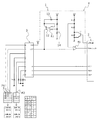
図1は、本発明の一実施形態に係る複数電圧判定回路を示しており、上記特許文献1に開示したものと同様の給湯装置における各種水位電極(負荷)の抵抗値がそれぞれの抵抗値判定閾値を超えているか否か、すなわち各水位電極が水に浸かっている(水有り)か浸かっていない(水無し)かを、各水位電極に定電流を供給したときに生じる電圧に基づいて判定するために好適に用いられるものである。
FIG. 1 shows a multiple voltage determination circuit according to an embodiment of the present invention, in which resistance values of various water level electrodes (loads) in a hot water supply apparatus similar to that disclosed in
図示例においては、3つの第1の水位電極P1と、1つの第2の水位電極P2が示されており、第1の水位電極P1(例えば中和器内に貯留するドレン水の水位を監視する水位電極など)は、水有り時(水に浸かっているとき)に300kΩ、水無し時(水に浸かっていないとき)に500kΩの抵抗値を示し、第2の水位電極P2(例えば、漏水検知用の水位電極など)は、水有り時に100kΩ、水無し時に300kΩの抵抗値を示すものとし、第1の水位電極P1の抵抗値判定閾値は400kΩ、第2の水位電極P2の抵抗値判定閾値は200kΩとする。また、水位電極P1,P2とは別に、後述するマルチプレクサ3の空きポートには固定抵抗Raがダミー負荷として接続されている。なお、上記抵抗値は本発明の理解のための例示にすぎず、適宜の抵抗値のものとして設計できる。
In the illustrated example, three first water level electrodes P1 and one second water level electrode P2 are shown, and the first water level electrode P1 (for example, the level of drain water stored in the neutralizer is monitored). The water level electrode or the like) has a resistance value of 300 kΩ when there is water (when immersed in water) and 500 kΩ when there is no water (when not immersed in water), and the second water level electrode P2 (for example, water leakage) The water level electrode for detection, etc.) has a resistance value of 100 kΩ when there is water and 300 kΩ when there is no water, the resistance value judgment threshold value of the first water level electrode P1 is 400 kΩ, and the resistance value judgment of the second water level electrode P2 The threshold is 200 kΩ. In addition to the water level electrodes P1 and P2, a fixed resistor Ra is connected as a dummy load to an empty port of the
本実施形態の複数電圧判定回路は、定電流源1と、上記複数の負荷P1,P2,Raのうちいずれか一の負荷を選択するための選択制御信号を出力する制御部としてのマイクロプロセッサ2と、前記選択制御信号によって選択される前記一の負荷に対して前記定電流源1が出力する定電流を供給するマルチプレクサ3(切替回路)と、前記定電流が供給されている前記一の負荷に生じる電圧レベルが所定の閾値を超えているか否かを判定してその判定結果信号をマイクロプロセッサ2に出力する比較回路4とを備えている。
The multiple voltage determination circuit of the present embodiment includes a constant
定電流源1は、例えば10μAの定電流を出力するものであり、図示例では、オペアンプ11と、該オペアンプ11の出力にベースが接続されたpnp型トランジスタ12と、該トランジスタ12のエミッタと電源(15V)との間に接続された出力側負荷抵抗13とを備え、トランジスタ12のエミッタはオペアンプ11の反転入力端子(−)に接続されて負帰還回路が構成されている。また、オペアンプ11の非反転入力端子(+)には、分圧回路14が出力する所定の出力電流設定用の電圧が入力されており、オペアンプ11の仮想短絡によって反転入力端子(−)の電圧と非反転入力端子(+)の電圧とが同電位となり、これにより出力側負荷抵抗13の両端電圧が定まって該抵抗13及びトランジスタ12を流れる電流が定まり、トランジスタ12のコレクタ出力から定電流が出力されるようになっている。
The constant
マイクロプロセッサ2は、給湯装置の各種給湯運転制御、暖房運転制御並びに追い焚き運転制御をも担うものであって、図1においては、本発明に関連する入出力ポートのみを示している。本実施形態では、上記選択制御信号は、マイクロプロセッサ2の3つの出力ポート(A出力ポート、B出力ポート及びC出力ポート)から出力される3ビットの論理信号によって構成されており、該選択制御信号は、マルチプレクサ3の対応する3つの制御信号入力ポート(A,B,C)にそれぞれ入力されている。
The
マルチプレクサ3は、ワンチップLSIの形態で市販されているアナログスイッチ式のものを採用することもできるし、汎用論理ゲート回路を用いて基板上に回路構成することもできる。本実施形態のマルチプレクサ3は、0〜7番の8つの入出力ポート(電圧入力部)と、一つの共通ポートCOM(電圧出力部)とを備えており、制御信号入力ポートA,B,Cに入力される選択制御信号に応じて8つの入出力ポートのうち図1に示した表に示す一つの入出力ポートを共通ポートCOMに導通させ、他の入出力ポートを共通ポートCOMから絶縁するよう構成されている。上記した3つの第1の水位電極P1は、マルチプレクサ3の0〜2番の入出力ポートにそれぞれ接続され、第2の水位電極P2は4番の入出力ポートに接続され、3番及び5〜7番の入出力ポートには固定抵抗Raがそれぞれ接続されている。なお、第2の水位電極P2を接続する入出力ポートは適宜のポートであってよい。選択制御信号によって選択された入出力ポートに接続されている負荷(本明細書において「選択制御信号によって選択された負荷」ということもある。)には、上記定電流源1が出力する定電流がマルチプレクサ3を介して供給され、各負荷の抵抗値に応じた検出電圧が当該負荷が接続されている入出力ポートに入力されて、該検出電圧が共通ポートCOMから出力される。
The
比較回路4は、比較器41と、該比較器41の負側入力端子に判定用の所定の基準電圧(閾値)を出力する分圧回路とを備えており、上記共通ポートCOMから出力される検出電圧は比較器41の正側入力端子に入力されている。
The
上記分圧回路は、直列接続された3つの抵抗器R1,R2,R3により構成されているとともに、オン時に抵抗器R3をバイパスするスイッチング素子としてのnpn型トランジスタQ1を備えており、該トランジスタQ1のオン時には電源電圧(15V)を2つの抵抗器R1,R2によって分圧してなる電圧(例えば2V)が比較器41の負側入力端子に基準電圧として入力され、トランジスタQ1のオフ時には、抵抗器R1の抵抗値と、2つの抵抗器R2,R3の合成抵抗値とにより分圧してなる電圧(例えば4V)が比較器41の負側入力端子に入力されるようになっている。そして、共通ポートCOMから出力される電圧が上記基準電圧を超えていれば比較器41が出力する判定信号はHigh信号となり、共通ポートCOMから出力される検出電圧が基準電圧を超えていなければ比較器41が出力する判定信号はLow信号となる。比較器41が出力する判定信号は、マイクロプロセッサ2のスキャン入力ポートに入力される。
The voltage dividing circuit includes three resistors R1, R2, and R3 connected in series, and includes an npn transistor Q1 as a switching element that bypasses the resistor R3 when turned on. The transistor Q1 When the transistor Q1 is turned on, a voltage (for example, 2V) obtained by dividing the power supply voltage (15V) by the two resistors R1 and R2 is input to the negative input terminal of the
マイクロプロセッサ2は、0〜7番の入出力ポートを反復的に順次選択するよう所定時間間隔毎(例えば数ミリ秒〜数十ミリ秒)に選択制御信号の内容を切り替え、各時点におけるスキャン入力ポートから入力する判定信号を、各入出力ポート毎に記憶手段に記憶するとともに、その判定信号を各種運転制御のパラメータとして用いるよう制御構成されている。また、上記分圧回路のトランジスタQ1は、マイクロプロセッサ2の閾値制御信号出力ポートから出力される閾値制御信号によってオン/オフ駆動されるよう回路構成されており、マイクロプロセッサ2は、第2の水位電極P2が接続された4番入出力ポートを選択する選択制御信号(A:1,B:0,C:0)の出力時にトランジスタQ1をオン制御し、その他の選択制御信号の出力時にはトランジスタQ1をオフ制御することにより、第2の水位電極P2の電圧の検出時には比較回路4の判定基準電圧(閾値)を2Vとし、第1の水位電極P1及び固定抵抗Raの電圧の検出時には基準電圧を4Vとするよう制御する。
The
かかる制御によって、水位電極P1の選択時には水有り時に300kΩ×10μA=3V、水無し時に500kΩ×10μA=5Vの電圧が共通ポートCOMから出力される一方、水位電極P2の選択時には水有り時に100kΩ×10μA=1V、水無し時に300kΩ×10μA=3Vの電圧が共通ポートCOMから出力されるが、各水位電極P1,P2毎に比較器41の電圧判定閾値(基準電圧)を適切なものに制御することによって、共通の比較器41によって水位電極P1に生じる電圧がその電圧判定閾値である4Vを超えているか否かを判定しつつ、水位電極P2に生じる電圧についてはその電圧判定閾値である2Vを超えているか否かの判定をも行うことができ、これにより回路構成の簡素化、部品点数の削減、ひいてはコスト低減を図ることができる。
With this control, when the water level electrode P1 is selected, a voltage of 300 kΩ × 10 μA = 3 V is output from the common port COM when there is water, and 500 kΩ × 10 μA = 5 V is output from the common port COM when there is no water. A voltage of 300 kΩ × 10 μA = 3 V is output from the common port COM when there is no water, but the voltage determination threshold (reference voltage) of the
また、本実施形態では、水位電極を接続しないマルチプレクサ3の入出力ポートには固定抵抗Raを接続しておくことで、マイクロプロセッサ2によるポートスキャン制御はすべての入出力ポートに対して行うよう制御構成することができ、他製品とのマイクロプロセッサ2のスキャン制御ソフトウェアの共通化を図ることができる。
Further, in the present embodiment, by connecting the fixed resistor Ra to the input / output port of the
また、固定抵抗Raを用いて、以下説明する制御方式によって比較回路4及びこれに関連する回路(マイクロプロセッサ2の閾値制御信号出力ポートの浮きや接続配線の不良など)の異常を検出することもできる。かかる異常検出制御について詳細に説明すると、固定抵抗Raの抵抗値として例えば330kΩのものを用いると、固定抵抗Raが接続されているいずれかの入出力ポート(定電圧入力部)を選択する選択制御信号が出力されていれば、該入出力ポートの入力電圧、及び、共通ポートCOMからの出力電圧は3.3Vの定電圧となる。したがって、比較回路4の電圧判定閾値(基準電圧)が上記定電圧よりも大きい4Vとなるように比較回路4を制御したときは比較回路4はLow出力となる。一方、比較回路4の電圧判定閾値(基準電圧)が上記定電圧よりも小さい2Vとなるように比較回路4を制御したときは比較回路4はHigh出力となる。
In addition, by using the fixed resistor Ra, an abnormality of the
しかし、比較回路4を構成する部品や配線のオープン故障などの異常が生じた場合、例えばスイッチング素子Q1のオープン故障時には、比較回路4の電圧判定閾値は閾値制御信号の内容にかかわらず4Vで固定されるため、電圧判定閾値を2Vとするように閾値制御信号としてHigh信号をスイッチング素子Q1に出力したとしても、固定抵抗Raの選択時の比較回路4の出力は定常的にLow出力となる。
However, when an abnormality such as an open failure of the components and wirings constituting the
したがって、固定抵抗Raの選択中に、電圧判定閾値が4Vとなるように比較回路4を制御した場合と、電圧判定閾値が2Vとなるように比較回路4を制御した場合とで、比較回路4の判定結果(出力信号)が異なるか否かに基づいて、比較回路4等の回路故障であるか否かを判定するようマイクロプロセッサ2を制御構成することによって、比較回路4等の回路故障を的確に検出できる。
Therefore, the
また、スイッチング素子Q1がショート故障した場合には、比較回路4の電圧判定閾値は2Vで固定されるため、この場合も、閾値制御信号にかかわらず比較回路4の判定結果が一定となり、これにより回路故障であると判定できる。
In addition, when the switching element Q1 is short-circuited, the voltage determination threshold value of the
なお、固定抵抗Raが複数取り付けられている場合には、いずれか一の固定抵抗Raのスキャン時に電圧判定閾値が4Vとなるよう制御する一方、他の固定抵抗Raのスキャン時に電圧判定閾値が2Vとなるよう制御して、それぞれの場合の比較回路4の判定結果が異なるか否かに基づいて故障判定を行わせることができる。また、一つの固定抵抗Raに対するスキャンタイミング毎に電圧判定閾値を変化させて、その判定結果が異なるか否かによって故障判定を行うこともできる。また、一つの固定抵抗Raに対する1回のスキャン時間が十分長い場合には、その1回のスキャン中に電圧判定閾値を変化させることで故障判定を行わせることも可能である。
When a plurality of fixed resistors Ra are attached, the voltage determination threshold is controlled to 4V when scanning any one of the fixed resistors Ra, while the voltage determination threshold is 2V when scanning other fixed resistors Ra. It is possible to make a failure determination based on whether or not the determination results of the
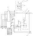
図2は本発明の別の実施形態に係る複数電圧判定回路を示しており、上記第1実施形態と同様の構成については同符号を付して詳細説明を省略し、異なる構成、作用効果について説明する。 FIG. 2 shows a multiple voltage determination circuit according to another embodiment of the present invention. The same components as those in the first embodiment are denoted by the same reference numerals and detailed description thereof is omitted. explain.
本実施形態の複数電圧判定回路では、マイクロプロセッサ2が出力する選択制御信号の各ビットは、ビット反転されてマルチプレクサ3の制御信号入力ポートA〜Cにそれぞれ入力されており、選択制御信号(マイクロプロセッサ2の出力信号)と、選択される入出力ポートとの関係は、図2に示す表に示す通りのものとなっている。
In the multiple voltage determination circuit of the present embodiment, each bit of the selection control signal output from the
また、本実施形態では、比較回路4の比較器41の入力が図1に示す実施形態とは正負反転され、負側入力端子にマルチプレクサ3の共通ポートCOMの出力電圧が入力され、正側入力端子に分圧回路の出力電圧が入力されている。また、スイッチング素子Q1オン時の分圧回路の出力電圧(比較回路4の電圧判定閾値)は4Vとされ、スイッチング素子Q1オフ時の分圧回路の出力電圧は7Vとされており、第2の水位電極P2は、水有り時に500kΩの抵抗値を示し、水無し時に900kΩの抵抗値を示し、その抵抗値判定閾値は700kΩとされ、10μAの電流を供給したときに生じる電圧としての電圧判定閾値が7Vとされている。
Further, in the present embodiment, the input of the
そして、マイクロプロセッサ2が出力する選択制御信号に基づいて、第2の水位電極P2が接続された4番入出力ポートが選択されている場合にのみ比較回路4のスイッチング素子Q1(本実施形態ではFET)をオフさせて比較回路4の電圧判定閾値(基準電圧)を7Vとし、その他の入出力ポートが選択されている場合にはスイッチング素子Q1をオンさせて比較回路4の電圧判定閾値を4Vとするよう回路構成されている。
Based on the selection control signal output from the
すなわち、スイッチング素子Q1の制御信号入力端子(ゲート)は、プルアップ抵抗R4を介して制御用電源(5V)に接続されるとともに、スイッチング素子Q3(図示例ではFET)を介してグラウンドに接続されており、該スイッチング素子Q3のオフ時はスイッチング素子Q1のゲートがプルアップされて該スイッチング素子Q1がオンし、スイッチング素子Q3のオン時はスイッチング素子Q1のゲートが接地されて該スイッチング素子Q1がオフする。 That is, the control signal input terminal (gate) of the switching element Q1 is connected to the control power supply (5V) via the pull-up resistor R4 and is connected to the ground via the switching element Q3 (FET in the illustrated example). When the switching element Q3 is off, the gate of the switching element Q1 is pulled up and the switching element Q1 is turned on. When the switching element Q3 is on, the gate of the switching element Q1 is grounded and the switching element Q1 is Turn off.
スイッチング素子Q3の制御信号入力端子(ゲート)は、プルアップ抵抗R5を介して制御用電源(5V)に接続されるとともに、スイッチング素子Q2(図示例ではnpn型トランジスタ。好ましくはデジタルトランジスタ。)を介してグラウンドに接続されており、スイッチング素子Q2のオフ時はスイッチング素子Q3のゲートがプルアップされて該スイッチング素子Q3がオンし、スイッチング素子Q2のオン時はスイッチング素子Q3のゲートが接地されて該スイッチング素子Q3がオフする。 The control signal input terminal (gate) of the switching element Q3 is connected to the control power supply (5V) via the pull-up resistor R5, and the switching element Q2 (npn type transistor in the illustrated example, preferably a digital transistor). When the switching element Q2 is off, the gate of the switching element Q3 is pulled up to turn on the switching element Q3. When the switching element Q2 is on, the gate of the switching element Q3 is grounded. The switching element Q3 is turned off.
スイッチング素子Q3のゲートは、逆起電圧防止用ダイオードD1並びに負荷抵抗R6を介して選択制御信号のA出力ポートに接続されているとともに、逆起電圧防止用ダイオードD2並びに負荷抵抗R7を介して選択制御信号のB出力ポートに接続されている。これにより、A出力ポート及びB出力ポートのいずれかがLow出力であれば、かかる出力ポートを介してスイッチング素子Q3のゲートが接地されてスイッチング素子Q3がオフし、スイッチング素子Q1がオンするようになっている。また、スイッチング素子Q2の制御信号入力端子(ベース)は、C出力ポートに接続されており、C出力ポートから出力される信号によってオン/オフ制御される。 The gate of the switching element Q3 is connected to the A output port of the selection control signal through the back electromotive voltage prevention diode D1 and the load resistor R6, and is selected through the back electromotive voltage prevention diode D2 and the load resistor R7. It is connected to the B output port of the control signal. As a result, if either the A output port or the B output port is Low output, the gate of the switching element Q3 is grounded through the output port so that the switching element Q3 is turned off and the switching element Q1 is turned on. It has become. Further, the control signal input terminal (base) of the switching element Q2 is connected to the C output port, and is on / off controlled by a signal output from the C output port.
かかる回路構成によって、A出力ポートがHigh出力、B出力ポートがHigh出力、C出力ポートがLow出力である場合にのみ、すなわち、4番入出力ポートが選択されているときのみスイッチング素子Q1がオフして比較回路4の電圧判定閾値が7Vとなり、その他のときはスイッチング素子Q1がオンして電圧判定閾値が4Vになる。
With this circuit configuration, the switching element Q1 is turned off only when the A output port is High output, the B output port is High output, and the C output port is Low output, that is, only when the fourth input / output port is selected. Thus, the voltage determination threshold value of the
本実施形態によれば、所定の負荷(第2の水位電極)を選択する選択制御信号を出力しているときに、この選択制御信号自体に基づいて比較回路4の電圧判定閾値を調節できるので、マイクロプロセッサ2の制御構成の簡素化を図ることができ、既存のマイクロプロセッサ2をそのまま流用して上記論理回路の追加のみで電圧判定閾値を調節することができ、マイクロプロセッサ2のソフト変更や出力ポートの追加等を行う必要がない。
According to this embodiment, when a selection control signal for selecting a predetermined load (second water level electrode) is output, the voltage determination threshold value of the
さらに、上記回路構成によれば、各スイッチング素子Q2,Q3や抵抗R6,R7などを基板上に実装するか非実装とするかによって、どの入出力ポートが選択されているときにスイッチング素子Q1をオンさせるかのバリエーションを変更できる。 Further, according to the above circuit configuration, when each input / output port is selected depending on whether each of the switching elements Q2, Q3 and the resistors R6, R7 are mounted on the substrate or not, the switching element Q1 is selected. You can change the variation of turning on.
例えば、図3に示すように負荷抵抗R6,R7をいずれも実装しなかった場合、スイッチング素子Q2のオン/オフのみに依存してスイッチング素子Q1がオン/オフするため、C出力ポートがHigh出力のときスイッチング素子Q1がオンし、C出力ポートがLow出力のときスイッチング素子Q1がオフする。したがって、図3に示す例では、0〜3番入出力ポートに第1の水位電極P1を接続でき、4〜7番入出力ポートに第2の水位電極P2を接続できる。 For example, as shown in FIG. 3, when neither of the load resistors R6 and R7 is mounted, the switching element Q1 is turned on / off depending only on the on / off of the switching element Q2, so that the C output port has a high output. When the switching element Q1 is ON, the switching element Q1 is turned OFF, and when the C output port is LOW output, the switching element Q1 is OFF. Therefore, in the example shown in FIG. 3, the first water level electrode P1 can be connected to the 0-3rd input / output port, and the second water level electrode P2 can be connected to the 4th-7th input / output port.
また、図4に示すように、負荷抵抗R7のみを実装しなかった場合は、0〜3,5,7番入出力ポートに第1の水位電極P1を接続でき、4及び6番入出力ポートに第2の水位電極P2を接続できる。 As shown in FIG. 4, when only the load resistor R7 is not mounted, the first water level electrode P1 can be connected to the 0th, third, fifth and seventh input / output ports, and the fourth and sixth input / output ports. To the second water level electrode P2.
また、図5に示すように、スイッチング素子Q2及び負荷抵抗R6を実装しなかった場合は、2,3,6,7番入出力ポートに第1の水位電極P1を接続でき、0,1,4,5番入出力ポートに第2の水位電極P2を接続できる。 Further, as shown in FIG. 5, when the switching element Q2 and the load resistor R6 are not mounted, the first water level electrode P1 can be connected to the second, third, sixth and seventh input / output ports. The second water level electrode P2 can be connected to the 4th and 5th input / output ports.
また、図6に示すように、負荷抵抗R6のみを実装しなかった場合は、0〜3,6,7番入出力ポートに第1の水位電極P1を接続でき、4,5番入出力ポートに第2の水位電極P2を接続できる。 Further, as shown in FIG. 6, when only the load resistor R6 is not mounted, the first water level electrode P1 can be connected to the 0th, 3rd, 6th, and 7th input / output ports, and the 4th, 5th input / output ports. To the second water level electrode P2.
また、図7に示すように、スイッチング素子Q2のみを実装しなかった場合は、1〜3,5〜7番入出力ポートに第1の水位電極P1を接続でき、0,4番入出力ポートに第2の水位電極P2を接続できる。 Further, as shown in FIG. 7, when only the switching element Q2 is not mounted, the first water level electrode P1 can be connected to the 1st, 3rd, 5th and 7th input / output ports, and the 0th and 4th input / output ports. To the second water level electrode P2.
また、図8に示すように、スイッチング素子Q2及び負荷抵抗R7を実装しなかった場合は、1,3,5,7番入出力ポートに第1の水位電極P1を接続でき、0,2,4,6番入出力ポートに第2の水位電極P2を接続できる。 In addition, as shown in FIG. 8, when the switching element Q2 and the load resistor R7 are not mounted, the first water level electrode P1 can be connected to the first, third, fifth and seventh input / output ports. The second water level electrode P2 can be connected to the 4th and 6th input / output ports.
なお、各抵抗R6,7又はスイッチング素子Q2を基板上に実装しないことに代えて、適宜の箇所にジャンパー線を設けて、各ジャンパー線を切断するか否かによって実質上上記と同様の回路構成とすることも可能である。 In place of not mounting the resistors R6, R7 or the switching element Q2 on the substrate, a circuit configuration substantially similar to the above is provided depending on whether or not each jumper wire is cut by providing jumper wires at appropriate locations. It is also possible.
本発明は、上記各実施形態に限定されるものではなく、適宜設計変更することができる。例えば、上記実施形態に係る複数電圧判定回路は、上記特許文献1に開示したものと同様の給湯装置の他、他の適宜の給湯器や温水暖房機器などに好適に適用できる。
The present invention is not limited to the above-described embodiments, and the design can be changed as appropriate. For example, the multiple voltage determination circuit according to the above embodiment can be suitably applied to other appropriate hot water heaters, hot water heaters, and the like in addition to the same hot water supply apparatus as that disclosed in
また、マルチプレクサ3は、上記実施形態では3ビットの選択制御信号によって8つの入出力ポートのいずれかに切り替えられるものを用いたが、2以上の入出力ポートを適宜の選択制御信号によって切替可能なものであればよい。また、マルチプレクサ3は、複数の電圧入力ポート(電圧入力部)と、共通の電圧出力ポートとを備え、選択制御信号によって選択された一の電圧入力ポートに入力される電圧に応じた電圧(入力電圧と同じ電圧、若しくは、入力電圧に比例する電圧など)を共通の電圧出力ポートから出力するものであればよく、選択された一の電圧入力ポートと出力ポートとの間をも電気的に絶縁されていてもよく、この場合は、マルチプレクサ3の電源電圧由来の電圧であって、一の電圧入力ポートへの入力電圧に応じた電圧を共通の電圧出力ポートから出力させるとともに、各負荷に電圧を生じさせる定電流源をマルチプレクサ3の電圧入力ポート側に設けるなど、適宜の回路構成とすることができる。
In the above-described embodiment, the
2 制御部
3 マルチプレクサ
4 比較回路
P1 負荷(第1の水位電極)
P2 負荷(第2の水位電極)
Ra 負荷(固定抵抗)
2
P2 load (second water level electrode)
Ra load (fixed resistance)
Claims (3)
前記マルチプレクサは、複数の電圧入力部と、前記制御部からの選択制御信号によって前記複数の電圧入力部から選択される一の電圧入力部に入力される電圧に応じた電圧を出力する電圧出力部とを備え、
前記比較回路は、前記電圧出力部から出力される電圧が所定の閾値を超えているか否かを判定する、複数電圧判定回路において、
前記比較回路は、いずれの電圧入力部が選択されているかによって前記閾値の大きさが前記制御部によって調節制御可能に構成されていることを特徴とする複数電圧判定回路。 A control unit, a multiplexer, and a comparison circuit;
The multiplexer includes a plurality of voltage input units and a voltage output unit that outputs a voltage corresponding to a voltage input to one voltage input unit selected from the plurality of voltage input units by a selection control signal from the control unit. And
In the multiple voltage determination circuit, the comparison circuit determines whether or not the voltage output from the voltage output unit exceeds a predetermined threshold.
The multiple voltage determination circuit, wherein the comparison circuit is configured such that the threshold value can be adjusted and controlled by the control unit depending on which voltage input unit is selected.
Priority Applications (1)
| Application Number | Priority Date | Filing Date | Title |
|---|---|---|---|
| JP2015248583A JP2017116277A (en) | 2015-12-21 | 2015-12-21 | Plural-voltages determination circuit |
Applications Claiming Priority (1)
| Application Number | Priority Date | Filing Date | Title |
|---|---|---|---|
| JP2015248583A JP2017116277A (en) | 2015-12-21 | 2015-12-21 | Plural-voltages determination circuit |
Publications (1)
| Publication Number | Publication Date |
|---|---|
| JP2017116277A true JP2017116277A (en) | 2017-06-29 |
Family
ID=59231626
Family Applications (1)
| Application Number | Title | Priority Date | Filing Date |
|---|---|---|---|
| JP2015248583A Pending JP2017116277A (en) | 2015-12-21 | 2015-12-21 | Plural-voltages determination circuit |
Country Status (1)
| Country | Link |
|---|---|
| JP (1) | JP2017116277A (en) |
Citations (10)
| Publication number | Priority date | Publication date | Assignee | Title |
|---|---|---|---|---|
| JPS5313771A (en) * | 1976-07-24 | 1978-02-07 | Kubota Ltd | Level detector |
| US4349882A (en) * | 1980-08-22 | 1982-09-14 | Veeder Industries Inc. | Liquid level measuring system |
| US4387434A (en) * | 1980-10-24 | 1983-06-07 | Process Technologies, Inc. | Intelligent field interface device for fluid storage facility |
| US4806847A (en) * | 1986-12-09 | 1989-02-21 | Caterpillar Inc. | Dielectric liquid level sensor and method |
| JPH03244431A (en) * | 1990-02-23 | 1991-10-31 | Funai Electric Co Ltd | Article washer |
| JPH0539462Y2 (en) * | 1990-01-29 | 1993-10-06 | ||
| JPH06194211A (en) * | 1992-12-22 | 1994-07-15 | Matsushita Electric Works Ltd | Liquid detection sensor |
| JPH08146011A (en) * | 1994-11-15 | 1996-06-07 | Toshiba Corp | Automatic chemical analyser |
| JP2002257617A (en) * | 2000-12-27 | 2002-09-11 | Mitsubishi Heavy Ind Ltd | Device for detecting height of liquid surface |
| JP2014109437A (en) * | 2012-11-30 | 2014-06-12 | Noritz Corp | Water level detection signal detector |
-
2015
- 2015-12-21 JP JP2015248583A patent/JP2017116277A/en active Pending
Patent Citations (10)
| Publication number | Priority date | Publication date | Assignee | Title |
|---|---|---|---|---|
| JPS5313771A (en) * | 1976-07-24 | 1978-02-07 | Kubota Ltd | Level detector |
| US4349882A (en) * | 1980-08-22 | 1982-09-14 | Veeder Industries Inc. | Liquid level measuring system |
| US4387434A (en) * | 1980-10-24 | 1983-06-07 | Process Technologies, Inc. | Intelligent field interface device for fluid storage facility |
| US4806847A (en) * | 1986-12-09 | 1989-02-21 | Caterpillar Inc. | Dielectric liquid level sensor and method |
| JPH0539462Y2 (en) * | 1990-01-29 | 1993-10-06 | ||
| JPH03244431A (en) * | 1990-02-23 | 1991-10-31 | Funai Electric Co Ltd | Article washer |
| JPH06194211A (en) * | 1992-12-22 | 1994-07-15 | Matsushita Electric Works Ltd | Liquid detection sensor |
| JPH08146011A (en) * | 1994-11-15 | 1996-06-07 | Toshiba Corp | Automatic chemical analyser |
| JP2002257617A (en) * | 2000-12-27 | 2002-09-11 | Mitsubishi Heavy Ind Ltd | Device for detecting height of liquid surface |
| JP2014109437A (en) * | 2012-11-30 | 2014-06-12 | Noritz Corp | Water level detection signal detector |
Similar Documents
| Publication | Publication Date | Title |
|---|---|---|
| US8680893B2 (en) | Circuits and techniques for load current control | |
| US20090154039A1 (en) | Overvoltage protection circuit and electronic device comprising the same | |
| US10452113B2 (en) | Power supply switch with programmable switching decision | |
| JP6299554B2 (en) | Power-on reset circuit | |
| KR102055854B1 (en) | Diagnostic system for a vehicle electrical system | |
| JP2014138303A (en) | Inductive load drive device | |
| KR20140023749A (en) | Reference voltage generation circuit of semiconductor apparatus | |
| JP5225785B2 (en) | Overcurrent protection circuit and power supply device using the same | |
| CN104204974A (en) | Sequencer analog output unit | |
| US7711971B1 (en) | Multi-input power supply supervisor | |
| JP2016095823A (en) | Voltage switching device | |
| KR101823287B1 (en) | Termination apparatus, termination control method, and storage medium on which termination control program has been stored | |
| US20120319663A1 (en) | Load-testing circuit for usb ports | |
| US8996894B2 (en) | Method of booting a motherboard in a server upon a successful power supply to a hard disk driver backplane | |
| KR20080009895A (en) | Charge and discharge circuit of smoothing capacitor | |
| JP2017116277A (en) | Plural-voltages determination circuit | |
| JP2014147044A (en) | Semiconductor integrated circuit | |
| TW201628306A (en) | Redundancy power control circuit and redundancy power supplying system using the same | |
| JP2008059145A (en) | Power supply device | |
| JP2017116278A (en) | Circuit for determining resistance values of multiple loads | |
| TWI680646B (en) | Keyboard apparatus | |
| KR20130051070A (en) | Majority decision circuit | |
| JP2013232760A (en) | Output driver circuit | |
| JP5193806B2 (en) | Comparator circuit and electronic equipment | |
| JP2014020796A (en) | Voltage abnormality detection circuit |
Legal Events
| Date | Code | Title | Description |
|---|---|---|---|
| RD03 | Notification of appointment of power of attorney |
Free format text: JAPANESE INTERMEDIATE CODE: A7423 Effective date: 20170727 |
|
| A621 | Written request for application examination |
Free format text: JAPANESE INTERMEDIATE CODE: A621 Effective date: 20181129 |
|
| A131 | Notification of reasons for refusal |
Free format text: JAPANESE INTERMEDIATE CODE: A131 Effective date: 20190820 |
|
| A977 | Report on retrieval |
Free format text: JAPANESE INTERMEDIATE CODE: A971007 Effective date: 20190821 |
|
| A02 | Decision of refusal |
Free format text: JAPANESE INTERMEDIATE CODE: A02 Effective date: 20200303 |