JP2017092017A - Luminous flux control member, light emitting device, surface light source device and display device - Google Patents
Luminous flux control member, light emitting device, surface light source device and display device Download PDFInfo
- Publication number
- JP2017092017A JP2017092017A JP2016010764A JP2016010764A JP2017092017A JP 2017092017 A JP2017092017 A JP 2017092017A JP 2016010764 A JP2016010764 A JP 2016010764A JP 2016010764 A JP2016010764 A JP 2016010764A JP 2017092017 A JP2017092017 A JP 2017092017A
- Authority
- JP
- Japan
- Prior art keywords
- light
- light emitting
- total reflection
- emitting element
- emitting device
- Prior art date
- Legal status (The legal status is an assumption and is not a legal conclusion. Google has not performed a legal analysis and makes no representation as to the accuracy of the status listed.)
- Pending
Links
Images


Classifications
-
- F—MECHANICAL ENGINEERING; LIGHTING; HEATING; WEAPONS; BLASTING
- F21—LIGHTING
- F21V—FUNCTIONAL FEATURES OR DETAILS OF LIGHTING DEVICES OR SYSTEMS THEREOF; STRUCTURAL COMBINATIONS OF LIGHTING DEVICES WITH OTHER ARTICLES, NOT OTHERWISE PROVIDED FOR
- F21V13/00—Producing particular characteristics or distribution of the light emitted by means of a combination of elements specified in two or more of main groups F21V1/00 - F21V11/00
- F21V13/02—Combinations of only two kinds of elements
- F21V13/04—Combinations of only two kinds of elements the elements being reflectors and refractors
-
- G—PHYSICS
- G02—OPTICS
- G02F—OPTICAL DEVICES OR ARRANGEMENTS FOR THE CONTROL OF LIGHT BY MODIFICATION OF THE OPTICAL PROPERTIES OF THE MEDIA OF THE ELEMENTS INVOLVED THEREIN; NON-LINEAR OPTICS; FREQUENCY-CHANGING OF LIGHT; OPTICAL LOGIC ELEMENTS; OPTICAL ANALOGUE/DIGITAL CONVERTERS
- G02F1/00—Devices or arrangements for the control of the intensity, colour, phase, polarisation or direction of light arriving from an independent light source, e.g. switching, gating or modulating; Non-linear optics
- G02F1/01—Devices or arrangements for the control of the intensity, colour, phase, polarisation or direction of light arriving from an independent light source, e.g. switching, gating or modulating; Non-linear optics for the control of the intensity, phase, polarisation or colour
- G02F1/13—Devices or arrangements for the control of the intensity, colour, phase, polarisation or direction of light arriving from an independent light source, e.g. switching, gating or modulating; Non-linear optics for the control of the intensity, phase, polarisation or colour based on liquid crystals, e.g. single liquid crystal display cells
- G02F1/133—Constructional arrangements; Operation of liquid crystal cells; Circuit arrangements
- G02F1/1333—Constructional arrangements; Manufacturing methods
- G02F1/1335—Structural association of cells with optical devices, e.g. polarisers or reflectors
- G02F1/1336—Illuminating devices
- G02F1/133602—Direct backlight
- G02F1/133605—Direct backlight including specially adapted reflectors
-
- G—PHYSICS
- G02—OPTICS
- G02F—OPTICAL DEVICES OR ARRANGEMENTS FOR THE CONTROL OF LIGHT BY MODIFICATION OF THE OPTICAL PROPERTIES OF THE MEDIA OF THE ELEMENTS INVOLVED THEREIN; NON-LINEAR OPTICS; FREQUENCY-CHANGING OF LIGHT; OPTICAL LOGIC ELEMENTS; OPTICAL ANALOGUE/DIGITAL CONVERTERS
- G02F1/00—Devices or arrangements for the control of the intensity, colour, phase, polarisation or direction of light arriving from an independent light source, e.g. switching, gating or modulating; Non-linear optics
- G02F1/01—Devices or arrangements for the control of the intensity, colour, phase, polarisation or direction of light arriving from an independent light source, e.g. switching, gating or modulating; Non-linear optics for the control of the intensity, phase, polarisation or colour
- G02F1/13—Devices or arrangements for the control of the intensity, colour, phase, polarisation or direction of light arriving from an independent light source, e.g. switching, gating or modulating; Non-linear optics for the control of the intensity, phase, polarisation or colour based on liquid crystals, e.g. single liquid crystal display cells
- G02F1/133—Constructional arrangements; Operation of liquid crystal cells; Circuit arrangements
- G02F1/1333—Constructional arrangements; Manufacturing methods
- G02F1/1335—Structural association of cells with optical devices, e.g. polarisers or reflectors
- G02F1/1336—Illuminating devices
- G02F1/133602—Direct backlight
- G02F1/133606—Direct backlight including a specially adapted diffusing, scattering or light controlling members
-
- G—PHYSICS
- G02—OPTICS
- G02F—OPTICAL DEVICES OR ARRANGEMENTS FOR THE CONTROL OF LIGHT BY MODIFICATION OF THE OPTICAL PROPERTIES OF THE MEDIA OF THE ELEMENTS INVOLVED THEREIN; NON-LINEAR OPTICS; FREQUENCY-CHANGING OF LIGHT; OPTICAL LOGIC ELEMENTS; OPTICAL ANALOGUE/DIGITAL CONVERTERS
- G02F1/00—Devices or arrangements for the control of the intensity, colour, phase, polarisation or direction of light arriving from an independent light source, e.g. switching, gating or modulating; Non-linear optics
- G02F1/01—Devices or arrangements for the control of the intensity, colour, phase, polarisation or direction of light arriving from an independent light source, e.g. switching, gating or modulating; Non-linear optics for the control of the intensity, phase, polarisation or colour
- G02F1/13—Devices or arrangements for the control of the intensity, colour, phase, polarisation or direction of light arriving from an independent light source, e.g. switching, gating or modulating; Non-linear optics for the control of the intensity, phase, polarisation or colour based on liquid crystals, e.g. single liquid crystal display cells
- G02F1/133—Constructional arrangements; Operation of liquid crystal cells; Circuit arrangements
- G02F1/1333—Constructional arrangements; Manufacturing methods
- G02F1/1335—Structural association of cells with optical devices, e.g. polarisers or reflectors
- G02F1/1336—Illuminating devices
- G02F1/133602—Direct backlight
- G02F1/133609—Direct backlight including means for improving the color mixing, e.g. white
-
- G—PHYSICS
- G02—OPTICS
- G02F—OPTICAL DEVICES OR ARRANGEMENTS FOR THE CONTROL OF LIGHT BY MODIFICATION OF THE OPTICAL PROPERTIES OF THE MEDIA OF THE ELEMENTS INVOLVED THEREIN; NON-LINEAR OPTICS; FREQUENCY-CHANGING OF LIGHT; OPTICAL LOGIC ELEMENTS; OPTICAL ANALOGUE/DIGITAL CONVERTERS
- G02F1/00—Devices or arrangements for the control of the intensity, colour, phase, polarisation or direction of light arriving from an independent light source, e.g. switching, gating or modulating; Non-linear optics
- G02F1/01—Devices or arrangements for the control of the intensity, colour, phase, polarisation or direction of light arriving from an independent light source, e.g. switching, gating or modulating; Non-linear optics for the control of the intensity, phase, polarisation or colour
- G02F1/13—Devices or arrangements for the control of the intensity, colour, phase, polarisation or direction of light arriving from an independent light source, e.g. switching, gating or modulating; Non-linear optics for the control of the intensity, phase, polarisation or colour based on liquid crystals, e.g. single liquid crystal display cells
- G02F1/133—Constructional arrangements; Operation of liquid crystal cells; Circuit arrangements
- G02F1/1333—Constructional arrangements; Manufacturing methods
- G02F1/1335—Structural association of cells with optical devices, e.g. polarisers or reflectors
- G02F1/1336—Illuminating devices
- G02F1/133602—Direct backlight
- G02F1/133606—Direct backlight including a specially adapted diffusing, scattering or light controlling members
- G02F1/133607—Direct backlight including a specially adapted diffusing, scattering or light controlling members the light controlling member including light directing or refracting elements, e.g. prisms or lenses
Abstract
Description
本発明は、発光素子から出射された光の配光を制御する光束制御部材、当該光束制御部材を有する発光装置、面光源装置および表示装置に関する。 The present invention relates to a light flux control member that controls light distribution of light emitted from a light emitting element, a light emitting device having the light flux control member, a surface light source device, and a display device.
液晶表示装置や看板などの透過型画像表示装置では、バックライトとして直下型の面光源装置を使用することがある。近年、光源として複数の発光素子を有する、直下型の面光源装置が使用されている(例えば、特許文献1参照)。 In a transmissive image display device such as a liquid crystal display device or a signboard, a direct type surface light source device may be used as a backlight. In recent years, a direct type surface light source device having a plurality of light emitting elements as a light source has been used (for example, see Patent Document 1).
特許文献1に記載の直下型光源装置(面光源装置)は、光源基板と、光源基板上に配置された、青色の光を出射する複数の光源(発光素子)と、複数の光源に対して空気層を介して配置された、蛍光体や量子ドットなどの波長変換物質を含む波長変換シートと、を有する。特許文献1に記載の面光源装置では、光源から出射された青色の光が波長変換シートの内部に入射すると、青色の光の一部が波長変換物質により赤色の光および緑色の光に変換される。青色の光、赤色の光および緑色の光は、混色されて白色の光となり、波長変換シートから出射される。
The direct type light source device (surface light source device) described in
しかしながら、特許文献1に記載の面光源装置には、蛍光体や量子ドットなどの高価な波長変換物質を使用するため、製造コストが高くなってしまうという問題がある。
However, since the surface light source device described in
製造コストを削減する手段としては、三原色を生成するための波長変化物質を用いる代わりに、出射光の色がそれぞれ異なる複数の発光素子を組み合わせて用いることが考えられる。しかしながら、出射光の色がそれぞれ異なる複数の発光素子を組み合わせて用いた場合、色ムラなく混色させることが必要となる。特に、面光源装置を薄型化または発光素子(光源)を広ピッチ化した場合、十分に混色させることが困難となり、色ムラが生じやすい。 As a means for reducing the manufacturing cost, it is conceivable to use a combination of a plurality of light emitting elements having different colors of the emitted light, instead of using the wavelength changing materials for generating the three primary colors. However, when a plurality of light emitting elements having different colors of emitted light are used in combination, it is necessary to mix colors without color unevenness. In particular, when the surface light source device is thinned or the light emitting elements (light sources) are widened, it is difficult to sufficiently mix colors, and color unevenness is likely to occur.
そこで、本発明の目的は、波長変換物質を用いることなく色ムラを抑制できる光束制御部材を提供することである。また、本発明の別の目的は、当該光束制御部材を有する、発光装置、面光源装置および表示装置を提供することである。 Therefore, an object of the present invention is to provide a light flux controlling member that can suppress color unevenness without using a wavelength converting substance. Another object of the present invention is to provide a light emitting device, a surface light source device, and a display device having the light flux controlling member.
本発明に係る光束制御部材は、発光素子から出射された光の配光を制御する光束制御部材であって、発光素子から出射された光を入射する入射面と、前記入射面を挟んで前記発光素子と対向する位置に形成され、前記入射面から入射した光の一部を、前記発光素子の光軸と略垂直であり、かつ互いに反対向きである2つの方向に反射させる第1全反射面と、前記入射面および前記第1全反射面を挟んで相対する位置に、前記入射面から入射した光の一部および前記第1全反射面で反射した光を前記入射面および前記第1全反射面から離れる方向にそれぞれ導光する2つの導光部と、前記2つの導光部の端部にそれぞれ配置され、前記光軸および前記光軸と交わり、前記2つの導光部が延在する方向に沿う第1仮想直線を含む仮想平面を境界として、前記仮想平面から離れるように、前記入射面で入射し直接到達した光を臨界角以上の角度で入射させ反射させる2つの第2全反射面と、前記2つの導光部のそれぞれの外面に形成され、前記導光部により導光された光をそれぞれ外部に出射する2つの出射面と、を有する。 A light flux controlling member according to the present invention is a light flux controlling member that controls light distribution of light emitted from a light emitting element, and includes an incident surface on which light emitted from the light emitting element is incident, and the incident surface sandwiching the incident surface. A first total reflection formed at a position facing the light emitting element and reflecting a part of light incident from the incident surface in two directions which are substantially perpendicular to the optical axis of the light emitting element and opposite to each other. A part of the light incident from the incident surface and the light reflected by the first total reflection surface at a position facing each other across the surface and the incident surface and the first total reflection surface. Two light guides for guiding light in a direction away from the total reflection surface and ends of the two light guides, respectively, intersect with the optical axis and the optical axis, and the two light guides extend. A virtual plane including the first virtual straight line along the existing direction is defined as a boundary. Two second total reflection surfaces that reflect light incident on the incident surface and directly reaching the incident surface at an angle greater than a critical angle so as to be away from the virtual plane, and outer surfaces of the two light guides, respectively. And two emission surfaces for emitting the light guided by the light guide part to the outside.
また、本発明に係る発光装置は、発光素子と、前記発光素子の光軸と交わるように配置された、本発明に係る光束制御部材と、を有する。 Moreover, the light-emitting device which concerns on this invention has a light-emitting element and the light beam control member which concerns on this invention arrange | positioned so that the optical axis of the said light-emitting element may be crossed.
また、本発明に係る面光源装置は、本発明に係る複数の発光装置と、前記発光装置から出射された光を拡散させつつ透過させる光拡散板と、を有し、前記複数の発光装置は、第1の方向に前記第1仮想直線が沿うように発光装置列として配置され、前記発光装置列は、前記第1の方向に垂直な第2の方向に複数列配置されている。 The surface light source device according to the present invention includes a plurality of light emitting devices according to the present invention, and a light diffusion plate that diffuses and transmits the light emitted from the light emitting devices, and the plurality of light emitting devices are The light emitting device rows are arranged so that the first virtual line is along the first direction, and the light emitting device rows are arranged in a plurality of rows in a second direction perpendicular to the first direction.
また、本発明に係る表示装置は、本発明に係る面光源装置と、前記面光源装置から出射された光を照射される被照射部材と、を有する。 Moreover, the display apparatus which concerns on this invention has the surface light source device which concerns on this invention, and the to-be-irradiated member irradiated with the light radiate | emitted from the said surface light source device.
本発明によれば、出射光の色がそれぞれ異なる複数の発光素子を光源とした場合に、波長変換物質を用いることなく色ムラを抑制できる光束制御部材を提供できる。また、当該光束制御部材を有する、色ムラの少ない発光装置、面光源装置および表示装置を提供することができる。 ADVANTAGE OF THE INVENTION According to this invention, when the light emitting element from which the color of each emitted light differs is used as the light source, the light beam control member which can suppress a color nonuniformity without using a wavelength conversion substance can be provided. Further, it is possible to provide a light emitting device, a surface light source device, and a display device that have the light flux controlling member and have little color unevenness.
以下、本発明の光束制御部材、発光装置、面光源装置および表示装置について、図面を参照して詳細に説明する。以下の説明では、本発明の面光源装置の代表例として、液晶表示装置のバックライトなどに適する面光源装置について説明する。これらの面光源装置は、面光源装置からの光を照射される被照射部材(例えば液晶パネル)と組み合わせることで、表示装置として使用されうる。 Hereinafter, a light flux controlling member, a light emitting device, a surface light source device, and a display device of the present invention will be described in detail with reference to the drawings. In the following description, a surface light source device suitable for a backlight of a liquid crystal display device will be described as a representative example of the surface light source device of the present invention. These surface light source devices can be used as a display device by combining with an irradiated member (for example, a liquid crystal panel) irradiated with light from the surface light source device.
[実施の形態1]
(面光源装置の構成)
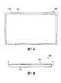
図1および図2は、本発明の実施の形態1に係る面光源装置100の構成を示す図である。図1Aは、面光源装置100の平面図であり、図1Bは、正面図である。図2は、図1Bに示されるA−A線の断面図である。図3は、発光装置130の断面図である。また、図4〜8は、実施の形態1に係る光束制御部材150の構成を示す図である。図4Aは、光束制御部材150の平面図であり、図4Bは、正面図であり、図4Cは、底面図である。図5Aは、光束制御部材150の右側面図であり、図5Bは、図4Aに示されるA−A線の断面図である。図6Aは、散乱部材157を外した光束制御部材150(光束制御部材本体)を上から見た斜視図であり、図6Bは、散乱部材157を外した光束制御部材150の底面158を上側に向けた場合の斜視図である。図7Aは、散乱部材157を外した光束制御部材150の平面図であり、図7Bは、正面図であり、図7Cは、底面図である。図8Aは、散乱部材157を外した光束制御部材150の右側面図であり、図8Bは、図7Aに示されるA−A線の断面図である。
[Embodiment 1]
(Configuration of surface light source device)
1 and 2 are diagrams showing the configuration of the surface
図1および図2に示されるように、面光源装置100は、筐体110、基板120、複数の発光装置130および光拡散板140を有する。
As shown in FIGS. 1 and 2, the surface
筐体110は、その内部に基板120および複数の発光装置130を収容するための、1つの面の少なくとも一部に開口部が設けられた直方体状の箱である。筐体110は、天板と、天板に対向する底板と、天板および底板を繋ぐ4つの側板とから構成される。天板には、発光領域となる長方形状の開口部が形成されている。この開口部は、光拡散板140により塞がれる。開口部の大きさは、光拡散板140に形成される発光領域(発光面)の大きさに相当し、例えば400mm×700mm(32インチ)である。底板と、光拡散板140とは、平行に配置されている。底板の表面から光拡散板140までの高さ(空間厚さ)は、特に限定されないが、10〜25mm程度である。そして、筐体110は、例えば、ポリメタクリル酸メチル(PMMA)やポリカーボネート(PC)などの樹脂や、ステンレス鋼やアルミニウムなどの金属などから構成される。
The
基板120は、発光装置130を筐体110内に所定の間隔で配置するための平板である。基板120は、筐体110の底板上に配置されている。基板120上に配置される発光装置130の数は、特に限定されない。基板120上に配置される発光装置130の数は、筐体110の開口部により規定される発光領域(発光面)の大きさに基づいて適宜設定される。発光装置130が配置される基板120の表面は、到達した光を光拡散板140に向けて反射させるように構成されている。
The
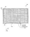
複数の発光装置130のそれぞれは、複数の発光素子131と、光束制御部材150とを有する。複数の発光装置130は、それぞれ発光素子131から出射される光の光軸OAが基板120の表面に対する法線に沿うように配置されている(図3参照)。複数の発光装置130は、第1の方向D1に発光装置130(光束制御部材150)の長軸(後述する第1仮想直線)が沿うように、発光装置列130Lとして配列されている。また、当該発光装置列130Lが第1の方向D1に直交する第2の方向D2に複数配置されている(図2参照)。また、発光装置130は、第2の方向D2に沿って見たときに、第2の方向D2において当該発光装置130を含む発光装置列130Lに隣接する発光装置列130Lに含まれる他の発光装置130に重なるように配置されている。ここで、「発光素子の光軸」とは、発光装置130の発光素子列131Lを構成する複数の発光素子131うち、中央の発光素子131からの立体的な光束の中心における光の進行方向を言う。
Each of the plurality of light emitting
発光素子131は、面光源装置100(および発光装置130)の光源である。発光素子131は、基板120上に配置されている。発光素子131は、例えば発光ダイオード(LED)である。1つの発光装置130に含まれる発光素子131の数は、1つまたは2つ以上である。本実施の形態では、1つの発光装置130に含まれる発光素子131の数は、3つである。また、各発光素子131から出射される出射光の色は、特に限定されない。さらに、複数の発光素子131を有する発光装置130において、各発光素子131から出射される出射光の色は、それぞれ異なっていてもよいし、すべて同じであってもよい。本実施の形態では、1つの発光装置130は、赤色の光を出射する発光素子131r、緑色の光を出射する発光素子131gおよび青色の光を出射する発光素子131bを有する。また、3つの発光素子131r、131g、131bは、発光装置130において、発光素子列131Lとなるように第1の方向D1に垂直な第2の方向D2に沿って配列されている(図2参照)。
The
発光装置130における複数の発光素子131の配列順序は、第1の方向D1または第2の方向D2において隣接する他の発光装置130における複数の発光素子131の配列順序と同じであってもよいし、異なっていてもよい。本実施の形態では、第2の方向D2において隣接する2つの発光装置130における複数の発光素子131の配列順序は、同じである。一方、第1の方向D1において隣接する2つの発光装置130における発光素子131の配列順序は、異なっている。
The arrangement order of the plurality of
具体的には、ある発光装置130では、第2の方向D2について、青色の光が出射される発光素子131b、緑色の光が出射される発光素子131g、赤色の光が出射される発光素子131rの順番となるように配列される。また、この発光装置130に第2の方向D2において隣接する発光装置130では、発光素子131の配列順序は、同じである。
Specifically, in a certain light
一方、この発光装置130に第1の方向D1において隣接する発光装置130では、赤色の光が出射される発光素子131r、緑色の光が出射される発光素子131g、青色の光が出射される発光素子131bの順番となるように配列される。
On the other hand, in the
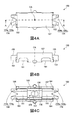
光束制御部材150は、発光素子131から出射された光の配光を制御する。図4〜図8に示されるように、光束制御部材150は、入射面151と、第1全反射面152と、2つの導光部153と、2つの第2全反射面154と、2つの出射面155と、脚部156と、散乱部材157とを有する。
The light
入射面151は、発光素子131から出射された光の一部を入射させる。入射面151は、光束制御部材150の底面(発光素子131側の面)158の中央部に形成された第1凹部159の内面である。第1凹部159の内面の形状は、特に限定されない。第1凹部159の内面は、半球状や半楕円体状などのように、エッジを含まない曲面であってもよいし、天面および側面を有するエッジを含む面であってもよい。本実施の形態では、第1凹部159の内面は、天面および側面を有する。
The
第1全反射面152は、入射面151を挟んで発光素子131と反対側(光拡散板140側)に配置されている。第1全反射面152は、入射面151から入射した光の一部を、発光素子131の光軸OA(光束制御部材150の中心軸CA)と略垂直であり、かつ互いに反対向きである2つの方向に反射させる。第1全反射面152は、光軸OAおよび光軸OAと交わり、2つの導光部153が延在する方向に沿う第1仮想直線を含む第1仮想平面で切断した断面において、中心軸CAから両端部に向かうにつれて、底面158(基板120)からの高さが高くなるように形成されている。より具体的には、第1全反射面152は、第1仮想平面で切断した断面において、中心軸CAから端部に向かうにつれて、接線の傾きが徐々に小さくなるようにそれぞれ形成されている。
The first
2つの導光部153は、入射面151および第1全反射面152を挟んで相対する位置に形成されている。導光部153は、入射面151で入射した光の一部および第1全反射面152で反射した光を、導光させながら少しずつ外部に出射させる。導光部153の光拡散板140側の面は、導光された光を外部に出射する出射面155として機能する。導光部153内には、出射面155から出射される光量を均一にする観点から、ビーズなどの散乱子が分散していてもよい。
The two
2つの第2全反射面154は、2つの導光部153の端部(中心軸CAから離れた端部)にそれぞれ配置されている。第2全反射面154は、光軸OA(中心軸CA)および第1仮想直線を含む第1仮想平面を境界として、第1仮想平面から離れるように、入射面151で入射し直接到達した光を臨界角以上の角度で入射させ反射させる。第2全反射面154の形状は、入射面151で入射した光のうち、一部の光が臨界角以上の角度で入射するように形成されていれば特に限定されない。本実施の形態では、第2全反射面154の形状は、光軸OAに垂直な第2仮想平面で切断した断面において、導光部153の端部から光軸OA(中心軸CA)に向かうにつれて第1仮想平面に近づくように形成された2つの傾斜面154a、154aを含む。言い換えると、本実施の形態では、第2全反射面154は、導光部153の端面おいて、光軸OA(中心軸CA)に沿う方向に配置されたV溝の対向する2つの内面である。導光部153を進行した光の一部は、第2全反射面154に到達する。第2全反射面154に到達する光は、様々な角度で入射し反射する。このとき、第2全反射面154に入射および反射することで、発光素子131から出射された赤、青、緑の色が混色される。
The two second total reflection surfaces 154 are arranged at the end portions (the end portions away from the central axis CA) of the two
出射面155は、第1仮想直線の延在方向において、中心軸CAに対して第1全反射面152より離れた位置にそれぞれ配置されている。出射面155は、入射面151で入射し、第1全反射面152で反射した後に導光部153を進行した光と、入射面で入射し、第1全反射面152で反射せずに導光部153を進行した光と、入射面で入射し、第1全反射面152で反射せずに導光部153を進行し、第2全反射面154で全反射した光とを外部に出射させる。また、出射面155には、光拡散処理(例えば、粗面化処理)が施されていてもよい。
The
導光部153の形状は、特に限定されない。本実施の形態では、導光部153は、略ロッド状の部材である。導光部153の短軸方向の断面積は、特に限定されない。本実施の形態では、導光部153の短軸方向の断面積は、第1全反射面152から第2全反射面154の中心軸CA側の端部までにおいて、第1全反射面152から離れるにつれて小さくなるように形成されている。また、2つの導光部153は、2つの補強部材160により連接されている。2つの補強部材160の下部には、2つの脚部156が配置されている。さらに、2つの導光部153の側面には、ガイド係合溝162がそれぞれ形成されている。
The shape of the
また、導光部153の底面(発光素子131側の面)158には、第2凹部161がそれぞれ形成されている。第2凹部161を形成することで、射出成形時におけるヒケの発生を抑制することができるとともに、製造コストを削減することができる。2つの第2凹部161は、いずれも光束制御部材150の長軸方向(第1仮想直線の延在方向)に沿って形成されているが、第1凹部159とは連通していない。第2凹部161の大きさおよび形状は、発光素子131から出射された光のうち、一部の光が第2全反射面154に直接到達することができるように形成され、かつ光束制御部材150に要求される強度を確保することができれば、特に限定されない。また、本実施の形態において、前述の機能を発揮できる範囲において、第2凹部161の平面視形状および深さも特に限定されず、適宜設定されうる。なお、光束制御部材150を射出成形により成形する場合、第2凹部161は、ヒケが発生するおそれがある部位に形成することが好ましい。
In addition,
補強部材160は、光束制御部材150の強度を向上させる。補強部材160の位置および形状は、光束制御部材150の第1全反射面152の機能を大きく阻害せず、かつ光束制御部材150の強度を向上させることができれば、特に限定されない。本実施の形態では、補強部材160は、光束制御部材150の底面(発光素子131側の面)158側に配置されており、導光部153同士を連接している。
The reinforcing
ガイド係合溝162は、第1仮想直線に沿う方向において、中心軸CAに対して補強部材160より離れた位置にそれぞれ配置されている。ガイド係合溝162は、後述する散乱部材157の係合突起164が係合することで、光束制御部材150に対して散乱部材157を位置決めするための溝である。
The
散乱部材157は、入射面151を挟んで発光素子131と反対側に配置されている。散乱部材157は、入射面151、第1全反射面152、導光部153、第2全反射面154および出射面155を含む光束制御部材本体とは、別部材である。散乱部材157は、主として第1全反射面152で反射せずに透過した光を拡散させつつ、透過させる。散乱部材157の形状は、前述の機能を発揮することができれば特に限定されない。散乱部材157の形状の例には、半円筒形状や釣り鐘様形状(逆U字型)などが含まれる。本実施の形態では、散乱部材157の形状は、鐘様形状である。また、散乱部材157の大きさも前述の機能を発揮できれば特に限定されない。散乱部材157は、第1全反射面152の上部のみを覆うように配置されていてもよいし、第1全反射面152および導光部153を覆うように形成されていてもよい。本実施の形態では、散乱部材157は、第1全反射面152と、出射面155の一部と、第2全反射面154の中心軸CA側の端部とを覆うように形成されている。散乱部材157の内面には、断面形状が略三角形または半円の複数のプリズム列163が配置されている。散乱部材157の発光素子131側の端部には、ガイド係合溝162と係合する係合突起164が配置されている。
The scattering
光束制御部材150の材料は、所望の波長の光を通過させ得るものであれば特に限定されない。たとえば、光束制御部材150の材料は、ポリメタクリル酸メチル(PMMA)やポリカーボネート(PC)、エポキシ樹脂(EP)などの光透過性樹脂、またはガラスである。
The material of the light
光拡散板140は、筐体110の開口部を塞ぐように配置されている。光拡散板140は、光拡散性を有する板状の部材であり、光束制御部材150からの出射光を拡散させつつ透過させる。通常、光拡散板140は、液晶パネルなどの被照射部材とほぼ同じ大きさである。たとえば、光拡散板140は、ポリメタクリル酸メチル(PMMA)、ポリカーボネート(PC)、ポリスチレン(PS)、スチレン・メチルメタクリレート共重合樹脂(MS)などの光透過性樹脂により形成される。光拡散性を付与するため、光拡散板140の表面に微細な凹凸が形成されているか、または光拡散板140の内部にビーズなどの光拡散子が分散している。
The
(シミュレーション)
次いで、発光装置130において、発光素子列131Lの中央に配置された発光素子131から出射された光の到達位置および光路についてシミュレーションを行った。
(simulation)
Next, in the
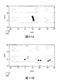
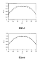
まず、各出射角度で発光素子131から出射され、光束制御部材150でその進行方向を制御された光の光拡散板140および基板120への到達位置をシミュレーションした。シミュレーションでは、3つの発光素子131を固定した基板120に、散乱部材157を組み付けた光束制御部材150を固定した発光装置130を用いた。また、基板120と光拡散板140との間隔は、12mmとした。さらに、3つの発光素子131のうち、中央部分に配置された1つの発光素子131のみを点灯した。なお、本シミュレーションでは、発光装置130における光路は、図4Aにおける中心軸CAを中心として、紙面左右方向(長軸方向)および紙面上下方向(短軸方向)において対称であるため、図4Aにおいて、中心軸CAに対して右上方向に出射される光の到達位置についてシミュレーションした。また、光軸OAに対する出射角度が30°、45°、60°および75°の5種類の出射角度で出射された光の到達位置についてシミュレーションした。また、各出射角度について、光軸OAに垂直な第2仮想平面で切断した断面において、第1仮想直線と平行な光を0°とし、第1仮想直線に対する角度が0°、5°、10°、15°、20°、25°、30°の7種類(合計で28種類)の光の到達位置についてシミュレーションした。また、比較のため、第2全反射面154を有さない光束制御部材(図示省略)を有する発光装置(以下、「比較例に係る発光装置」ともいう)についても同様にシミュレーションした。
First, the arrival position of the light, which is emitted from the
図9、11、13および15は、各出射角度で発光素子131から出射され、光束制御部材150で制御された光の光拡散板140および基板120への到達位置を示した図である。
9, 11, 13, and 15 are views showing the positions where the light emitted from the
図9Aは、30°の出射角度で発光素子から出射され、光束制御部材で制御された光の光拡散板140への到達位置を示した図であり、図9Bは、当該光の基板120への到達位置を示した図である。図11Aは、45°の出射角度で発光素子から出射され、光束制御部材で制御された光の光拡散板140への到達位置を示した図であり、図11Bは、当該光の基板120への到達位置を示した図である。図13Aは、60°の出射角度で発光素子から出射され、光束制御部材で制御された光の光拡散板140への到達位置を示した図であり、図13Bは、当該光の基板120への到達位置を示した図である。図15Aは、75°の出射角度で発光素子から出射され、光束制御部材で制御された光の光拡散板140への到達位置を示した図であり、図15Bは、当該光の基板120への到達位置を示した図である。
FIG. 9A is a diagram showing the arrival position of the light emitted from the light emitting element at an emission angle of 30 ° and controlled by the light flux controlling member, and FIG. 9B shows the light to the
図9、11、13および15における横軸および縦軸は、発光点(発光素子131の中心)からの光軸OAに直交する方向についての距離(mm)を示している。また、図9、11、13および15には、平面視したときの発光装置130の位置を点線で示している。図9、11、13および15におけるXのシンボルは、本実施の形態に係る発光装置130から出射された光の到達位置を示しており、黒三角のシンボルは、比較例に係る発光装置から出射された光の到達位置を示しており、黒丸のシンボルは、基板120上に発光素子131のみを配置した場合の光の到達位置を示している。
9, 11, 13 and 15, the horizontal axis and the vertical axis indicate the distance (mm) in the direction perpendicular to the optical axis OA from the light emitting point (the center of the light emitting element 131). 9, 11, 13 and 15, the position of the
次に、各出射角度で発光素子131から出射された光の発光装置130における光路についてシミュレーションした。本シミュレーションでは、第2仮想平面で切断した平面における光線の本数が、前述のシミュレーションと異なる。なお、本明細書では、比較例に係る発光装置については、出射角度が45°および75°場合の結果のみを示す。
Next, an optical path in the
図10、12、14および16は、各出射角度で発光素子131から出射された光の発光装置130における光路図である。また、図17は、比較例に係る発光装置における光路図である。図10Aは、30°の出射角度で発光素子131から出射された光の発光装置130を正面視したときの光路図であり、図10Bは、平面視したときの光路図である。図12Aは、45°の出射角度で発光素子131から出射された光の発光装置130を正面視したときの光路図であり、図12Bは、平面視したときの光路図である。図14Aは、60°の出射角度で発光素子131から出射された光の発光装置130を正面視したときの光路図であり、図14Bは、平面視したときの光路図である。図16Aは、75°の出射角度で発光素子131から出射された光の発光装置130を正面視したときの光路図であり、図16Bは、平面視したときの光路図である。図17Aは、45°の出射角度で発光素子131から出射された光の比較例に係る発光装置を正面視したときの光路図であり、図17Bは、平面視したときの光路図であり、図17Cは、75°の出射角度で発光素子131から出射された光の比較例に係る発光装置を正面視したときの光路図であり、図17Dは、平面視したときの光路図である。
10, 12, 14 and 16 are optical path diagrams in the
図9Bおよび図10A、Bに示されるように、出射角度が30°の場合では、本実施の形態に係る発光装置130から出射される光と、比較例に係る発光装置から出射される光は、いずれも基板120に到達することが分かった。また、比較例に係る発光装置から出射された光は、第1仮想直線に沿う方向に出射された。一方、本実施の形態に係る発光装置130から出射された光は、光軸OAおよび第1仮想直線に垂直な方向に出射されることが分かった。また、特にシミュレーションの結果は示していないが、発光装置130に出射光の色がそれぞれ異なる3つの発光素子131を配置し、当該3つの発光素子131を点灯させた場合では、各発光素子131から出射される光は、それぞれ光路が交差することによって混色される。したがって、光拡散板140には、混色された光が到達するため、色ムラを抑制することができた。
As shown in FIG. 9B and FIGS. 10A and 10B, when the emission angle is 30 °, the light emitted from the
図11B、図12A、Bおよび図17A、Bに示されるように、出射角度が45°の場合では、本実施の形態に係る発光装置130から出射される光と、比較例に係る発光装置から出射される光は、主として基板120に到達することが分かった。また、本実施の形態に係る発光装置130から出射された光は、光軸OAおよび第1仮想直線に垂直な方向に出射されることが分かった。一方、比較例に係る発光装置から出射された光は、第1仮想直線に沿う方向に出射された。なお、出射角度が45°の場合であって、本実施の形態に係る発光装置130から出射された光は、出射角度が30°の場合の本実施の形態に係る発光装置130から出射される光と比較して、中心軸CA側に出射されることが分かった(図11B参照)。また、この場合も3つの発光素子131を点灯させた発光装置130では、各発光素子131から出射される光は、それぞれ光路が交差することによって混色される。したがって、光拡散板140には、混色された光が到達する。
As shown in FIG. 11B, FIG. 12A, B and FIGS. 17A, B, when the emission angle is 45 °, the light emitted from the
図13Bおよび図14A、Bに示されるように、出射角度が60°の場合では、本実施の形態に係る発光装置130から出射される光と、比較例に係る発光装置から出射される光とは、基板120に到達する光よりも光拡散板140に到達する光が多いことが分かった。また、本実施の形態に係る発光装置130から出射された光は、光軸OAおよび第1仮想直線に垂直な方向に出射されることが分かった。一方、比較例に係る発光装置から出射された光は、第1仮想直線に沿う方向に出射されることが分かった。また、この場合も3つの発光素子131を点灯させた発光装置130では、各発光素子131から出射される光は、それぞれ光路が交差することによって混色される。したがって、光拡散板140には、混色された光が到達する。
As shown in FIG. 13B and FIGS. 14A and B, when the emission angle is 60 °, the light emitted from the
図15B、図16Bおよび図17C、Dに示されるように、出射角度が75°の場合では、本実施の形態に係る発光装置130から出射される光と、比較例に係る発光装置から出射される光とは、光拡散板140に到達する光よりも基板120に到達する光が多いことが分かった。また、本実施の形態に係る発光装置130から出射された光は、光軸OAおよび第1仮想直線に垂直な方向に出射されることが分かった。一方、比較例に係る発光装置から出射された光は、光軸OAおよび第1仮想直線に沿う方向に出射されることが分かった。また、この場合も3つの発光素子131を点灯させた発光装置130では、各発光素子131から出射される光は、それぞれ光路が交差することによって混色される。したがって、光拡散板140には、混色された光が到達する。
As shown in FIGS. 15B, 16B, 17C, and 17D, when the emission angle is 75 °, the light emitted from the
また、図9A、図11A、図13Aおよび図15Aに示されるように、基板120に発光素子131のみを固定した場合には、発光素子131から出射した光は、すべて光拡散板140に到達することが分かった。
9A, FIG. 11A, FIG. 13A, and FIG. 15A, when only the
また、図9A、図11A、図13Aおよび図15Aに示されるように、発光素子131から出射される光は、第1の方向D1および第2の方向D2に向かって出射されていることが分かる。また、比較例に係る光束制御部材は、第2の方向への出射を抑制するように機能している。比較例に係る光束制御部材のように、第2の方向D2への出射を抑制すると、第2の方向D2において、発光装置130間に暗部が生じやすくなってしまう。そこで、本発明に係る光束制御部材150では、第2全反射面154により、導光部153を進行する光のうち、一部の光を第2の方向に向けて出射するように制御している。これにより、第2の方向D2における発光装置130間に生じやすい暗部の発生を抑制している。
Further, as shown in FIGS. 9A, 11A, 13A, and 15A, it is understood that the light emitted from the
(効果)
以上のように、本実施の形態に係る光束制御部材150では、2つの第2全反射面154を有するため、導光部153を進行してきた光を第1仮想平面から離れるように制御する。また、発光装置130における各発光素子131からの出射光は、互いに交差して、光拡散板140に到達する。これにより、出射光の色がそれぞれ異なる複数の発光素子131を光源とした場合であっても、各発光素子131から出射された色を混色することができる。よって、当該光束制御部材150を有する発光装置130、面光源装置100および表示装置では、暗部の発生を抑制できるとともに、色ムラを抑制することができる。
(effect)
As described above, since light
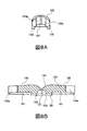
(変形例)
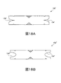
図18A、Bは、本発明の一実施の形態の変形例に係る光束制御部材の第2全反射面を説明するための図である。図18Aは、散乱部材157を外した変形例1に係る光束制御部材150’の平面図であり、図18Bは、散乱部材157を外した変形例2に係る光束制御部材150”の平面図である。図18Aに示されるように、第2全反射面154’の第2仮想平面で切断した断面形状は、第1仮想直線に向かって凸の曲線であってもよい。また、図18Bに示されるように、第2全反射面154”の第2仮想平面で切断した断面形状は、第1仮想直線に向かって凸の曲線であってもよい。また、第2全反射面154”の第1仮想平面および第2仮想平面に直交する第3仮想平面で切断した断面形状は、底面158側に凸の曲線であってもよいし、底面158側に凹の曲線であってもよい。
(Modification)
18A and 18B are views for explaining the second total reflection surface of the light flux controlling member according to the modification of the embodiment of the present invention. FIG. 18A is a plan view of a light
また、上記実施の形態では、光束制御部材150は、入射面151と、第1全反射面152と、2つの導光部153と、2つの第2全反射面154と、2つの出射面155と、脚部156と、散乱部材157とを有していたが、散乱部材157を有していなくてもよい。すなわち、光束制御部材は、入射面151と、第1全反射面152と、2つの導光部153と、2つの第2全反射面154と、2つの出射面155と、脚部156とから構成されていてもよい。この場合であっても、第2の方向D2における暗部の発生を抑制できるとともに、色ムラを抑制することができる。
In the above embodiment, the light
[実施の形態2]
実施の形態2に係る面光源装置は、第2の方向D2における光拡散板140上の輝度ムラをさらに抑制できるものである。実施の形態2に係る面光源装置は、発光装置の光束制御部材250の構成が実施の形態1に係る面光源装置100と異なる。そこで、実施の形態1に係る面光源装置100と同様の構成については、同様の符号を付してその説明を省略する。
[Embodiment 2]
The surface light source device according to
(面光源装置の構成)
実施の形態2に係る面光源装置は、筐体110、基板120、複数の発光装置130および光拡散板140を有する。複数の発光装置130は、第1の方向D1に発光装置130(光束制御部材250)の長軸が沿うように、発光装置列130Lとして配列されている。また、当該発光装置列130Lが第2の方向D2に複数配置されている(図2参照)。また、発光装置130は、第2の方向D2に沿って見たときに、第2の方向D2において当該発光装置130を含む発光装置列130Lに隣接する発光装置列130Lに含まれる他の発光装置130に重なるように配置されている。さらに、複数の発光装置列130Lは、第2の方向D2において、隣接する2つの発光装置列130Lの間隔が一定となるように配置されている。
(Configuration of surface light source device)
The surface light source device according to
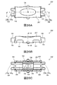
(光束制御部材の構成)
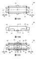
図19〜図22は、実施の形態2に係る光束制御部材250の構成を示す図である。図19Aは、光束制御部材250の平面図であり、図19Bは、正面図であり、図19Cは底面図である。また、図20Aは、光束制御部材250の右側面図であり、図20Bは、図19Bに示されるB−B線の断面図であり、図20Cは、図19Aに示されるA−A線の断面図である。図21Aは、散乱部材257の平面図であり、図21Bは、正面図であり、図21Cは、底面図である。図22は、散乱部材257の特徴を説明するための図である。なお、図22では、光束制御部材本体を省略している。
(Configuration of luminous flux control member)
19-22 is a figure which shows the structure of the light
図19〜図21に示されるように、光束制御部材250は、入射面151と、第1全反射面152と、2つの導光部153と、2つの第2全反射面154と、2つの出射面155と、脚部156と、散乱部材257とを有する。
As shown in FIGS. 19 to 21, the light
散乱部材257は、入射面151、第1全反射面152、導光部153、第2全反射面154および出射面155を含む光束制御部材本体とは、別部材である。散乱部材257は、主として第1全反射面152で反射せずに透過した光を拡散させつつ、透過させる。実施の形態2に係る散乱部材257の断面形状は、釣り鐘様形状(逆U字型)である。すなわち、第2の方向D2に平行な断面において、散乱部材257の内面の一部は、略半円状である。散乱部材257の内面には、断面形状が略半円の複数のプリズム列163が配置されている。散乱部材257の発光素子131側の端部には、ガイド係合溝162と係合する係合突起164が配置されている。一方、散乱部材257の外面は、後述する所定の形状となっている。
The scattering
ここで、図22を参照して、実施の形態2に係る光束制御部材250の散乱部材257の特徴について説明する。ここでは、図22に示されるように、光軸OAを含み第1仮想直線に垂直な第3仮想平面で散乱部材257を切断した断面について考える。光拡散板140の発光素子131側の面上を第2の方向に移動可能な点Aがあるとする。また、発光素子131の光軸OAと、光拡散板140の発光素子131側の面とが交わる点を交点Pとする。また、光拡散板140の発光素子131側の面上における隣接する2つの発光装置列130Lの中点を中間点Qとする。さらに、発光素子131の発光中心と点Aを結ぶ直線を第4仮想直線とする。なお、以下の説明では、光軸OAと、発光素子131の発光中心および中間点Qを結ぶ仮想直線と、がなす角度のうち、小さい角度を「中点角度」ともいう。
Here, with reference to FIG. 22, the characteristics of the scattering
点Aを交点Pから中間点Qまで移動させるとき、第4仮想直線上における散乱部材257の厚さは、点Aが交点Pから中間点Qに向かうにつれて厚くなるように形成されている。なお、本実施の形態では、点Aが中間点Q上に位置しているときの第4仮想直線上における散乱部材257の厚さが最も厚くなるように形成されている。すなわち、点Aが中間点Qを通り過ぎた後の第4仮想直線上における散乱部材257の厚さは、点Aが中間点Q上に位置しているときの第4仮想直線上における散乱部材257の厚さと同じかそれよりも薄い。なお、以下の説明では、第4仮想直線上における散乱部材257の厚さが最も厚くなる場合における、光軸OAおよび第4仮想直線がなす角度のうち、小さい角度を「最大厚み角度」ともいう。たとえば、このような形状を満たす散乱部材257は、第3仮想平面で切断した断面において、散乱部材257の外面の曲率は、散乱部材257の内側の曲率より小さくなるように形成されている。たとえば、当該断面における散乱部材257の内側の曲率を1とした場合、当該断面における散乱部材257の外面の曲率は、0.5倍である。また、第4仮想直線上における散乱部材257の厚さが前述の条件を満たせば、散乱部材257を第3仮想平面で切断したときの内面および外面は、弧でなくてもよい。たとえば、散乱部材257の内面は円弧であり、外面は複数の直線であってもよい。
When the point A is moved from the intersection point P to the intermediate point Q, the thickness of the scattering
なお、実施の形態1では、点Aを交点Pから中間点Qまで移動させるとき、第4仮想直線L上における散乱部材157の厚さは、一定となるように形成されている(図5A参照)。
In the first embodiment, when the point A is moved from the intersection point P to the intermediate point Q, the thickness of the scattering
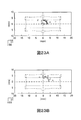
(シミュレーション)
次いで、発光素子列131Lの中央に配置された発光素子131から出射された光の光拡散板140上における到達位置についてシミュレーションを行った。
(simulation)
Next, a simulation was performed on the arrival position on the
本シミュレーションでは、3つの発光素子131を固定した基板120に、散乱部材257を組み付けた装置を用いた。すなわち、本シミュレーションでは、光束制御部材本体を使用しておらず、散乱部材257の効果のみを調べた。また、基板120と光拡散板140との間隔は、12mmとした。さらに、3つの発光素子131のうち、中央部分に配置された1つの発光素子131のみを点灯した。なお、本シミュレーションにおける光路は、図19Aにおける中心軸CAを中心として、紙面左右方向(長軸方向)および紙面上下方向(短軸方向)においてそれぞれ対称であるため、図19Aにおいて、中心軸CAに対して右上方向に出射される光の到達位置についてシミュレーションした。また、光軸OAに対する出射角度が15°、20°、25°および30°の4種類の出射角度で出射された光の到達位置についてシミュレーションした。また、各出射角度について、光軸OAに垂直な第2仮想平面で切断した断面において、第1仮想直線と平行な光を0°とし、第1仮想直線に対する角度が0°、15°、30°、45°、60°、75°、90°の7種類(合計で28種類)の光の到達位置についてシミュレーションした。なお、シミュレーションに使用した散乱部材は、実施の形態1に係る光束制御部材150の散乱部材157と、実施の形態2に係る光束制御部材250の散乱部材257を使用した。
In this simulation, an apparatus in which the
図23および図24は、各出射角度で発光素子131から出射され、散乱部材157、257で制御された光の光拡散板140への到達位置を示した図である。
FIGS. 23 and 24 are views showing the arrival positions of the light emitted from the
図23Aは、15°の出射角度で発光素子131から出射され、散乱部材157、257で制御された光の光拡散板140への到達位置を示した図であり、図23Bは、20°の出射角度で発光素子131から出射され、散乱部材157、257で制御された光の光拡散板140への到達位置を示した図である。また、図24Aは、25°の出射角度で発光素子131から出射され、散乱部材157、257で制御された光の光拡散板140への到達位置を示した図であり、図24Bは、30°の出射角度で発光素子から出射され、散乱部材157、257で制御された光の光拡散板140への到達位置を示した図である。
FIG. 23A is a diagram showing the position where the light emitted from the
図23および図24における横軸および縦軸は、発光点(発光素子131の中心)からの光軸OAに直交する方向についての距離(mm)を示している。また、図23および図24には、平面視したときの散乱部材257の位置を点線で示している。図23および図24における黒丸のシンボルは、基板120上に発光素子131のみを配置した場合の光の到達位置を示しており、白抜き三角のシンボルは、実施の形態1に係る散乱部材157で制御された光の到達位置を示しており、白抜き四角のシンボルは、実施の形態2に係る散乱部材257で制御された光の到達位置を示している。
The horizontal axis and the vertical axis in FIGS. 23 and 24 indicate the distance (mm) in the direction orthogonal to the optical axis OA from the light emitting point (center of the light emitting element 131). Moreover, in FIG. 23 and FIG. 24, the position of the scattering
図23Aおよび図23Bに示されるように、発光素子131からの出射角が15°および20°の角度で出射した光は、散乱部材を使用しない場合より散乱部材157、257を使用した場合の方が散乱部材157、257の長手方向(第1の方向D1)に拡がるように制御されていることが分かる。また、図24Aおよび図24Bに示されるように、発光素子131からの出射角が25°および30°の角度で出射した光は、散乱部材を使用しない場合より散乱部材157、257を使用した場合の方が、長手方向(第1の方向D1)だけでなく散乱部材157、257の短手方向(第2の方向D2)にも拡がるように制御されていることが分かる。
As shown in FIG. 23A and FIG. 23B, the light emitted from the
次いで、光束制御部材本体および散乱部材157、257を組み合わせた光束制御部材150、250含む発光装置を用いた面光源装置における輝度分布についてシミュレーションした。本シミュレーションでは、第3仮想平面で切断した断面において、光拡散板140上の第3仮想平面との交線上における輝度分布を求めた。なお、本シミュレーションにおいて中点角度は、30°である。
Next, the luminance distribution in the surface light source device using the light emitting device including the light
なお、シミュレーションに使用した発光装置は、実施の形態1に係る発光装置130と、実施の形態2に係る発光装置とを使用した。また、比較のため、前述した第4仮想直線上における散乱部材の厚さが最も厚くなるときの点Aの位置が、交点Pおよび中間点Qとの間に位置する発光装置A、Bについてもシミュレーションした。発光装置Aは、最大厚み角度が23°の散乱部材を有する発光装置であり、発光装置Bは、最大厚み角度が15°の散乱部材を有する発光装置である。
In addition, the light-emitting device used for the simulation used the light-emitting
図25A、Bは、第3仮想平面との交線上における、光拡散板140上の輝度分布を示したグラフである。図25Aは、実施の形態1に係る発光装置130および実施の形態2に係る発光装置における輝度分布を示しており、図25Bは、実施の形態1に係る発光装置130、発光装置Aおよび発光装置Bにおける輝度分布を示している。図25A、Bの横軸は、光軸OAに対する発光素子131の発光中心および光拡散板140上の点を結ぶ仮想直線の角度(°)を示しており、縦軸は、最大値を「1」として規格化した輝度をそれぞれ示している。図25A、Bの破線は、実施の形態1に係る発光装置130の結果を示しており、図25Aの実線は、実施の形態2に係る発光装置の結果を示しており、図25Bの一点鎖線は、発光装置Aの結果を示しており、図25Bの二点鎖線は、発光装置Bの結果を示している。
25A and 25B are graphs showing the luminance distribution on the
図25Aに示されるように、中点角度と、最大厚み角度と、が同じ角度(30°)である本実施の形態に係る発光装置では、30°近傍に輝度のピークがあることが分かる。これにより、第2の方向D2に中点角度が30°となるように発光装置が一定間隔で配置された面光源装置において、各発光装置は、発光素子131の直上部から第2の方向D2に隣接する2つの中間点Qまでの範囲を均一に照らすことができることが分かる。また、特にシミュレーションの結果は示していないが、発光装置に出射光の色がそれぞれ異なる3つの発光素子131を配置し、当該3つの発光素子131を点灯させた場合では、各発光素子131から出射される光は、それぞれ光路が交差することによって混色される。したがって、光拡散板140には、混色された光が到達するため、色ムラを抑制することができた。よって、このような発光装置を有する面光源装置では、全体で発光装置列間に輝度ムラが少なく、かつ色ムラを抑制できることが示唆される。一方、中点角度より最大厚み角度が小さい発光装置A、Bでは、輝度のピークの角度が30°未満であった。これは、第2の方向D2に中間角度が30°となるように発光装置が配置された面光源装置では発光装置列間に輝度ムラが生じてしまうことを示している。
As shown in FIG. 25A, it can be seen that in the light emitting device according to the present embodiment in which the midpoint angle and the maximum thickness angle are the same angle (30 °), there is a luminance peak in the vicinity of 30 °. Thus, in the surface light source device in which the light emitting devices are arranged at a constant interval so that the midpoint angle is 30 ° in the second direction D2, each light emitting device is arranged in the second direction D2 from directly above the
(効果)
以上のように、本実施の形態に係る面光源装置では、中点角度と最大厚み角度とが同じ角度となるように光束制御部材250が形成されている。よって、実施の形態1に係る効果に加え、さらに発光装置列間の輝度ムラを抑制することができる。
(effect)
As described above, in the surface light source device according to the present embodiment, light
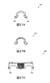
(変形例)
図26および図27は、実施の形態2の変形例に係る光束制御部材250’の構成を示す図である。図26Aは、実施の形態2の変形例に係る光束制御部材250’の平面図であり、図26Bは、正面図であり、図26Cは、底面図である。また、図27Aは、光束制御部材350の右側面図であり、図27Bは、図26Bに示されるB−B線の断面図であり、図27Cは、図26Aに示されるA−A線の断面図である。
(Modification)
FIG. 26 and FIG. 27 are diagrams showing a configuration of a light
図26および図27に示されるように、実施の形態2の変形例に係る光束制御部材250’の散乱部材257’の外面に凹部が形成されていてもよい。この場合も、散乱部材257’は、第3仮想平面で切断した断面において、最大厚み角度と中点角度が同じ角度となるように形成される。また、特に図示しないが、実施の形態2の変形例に係る光束制御部材250’を有する面光源装置は、光拡散板140を均一に照らすことができた。
As shown in FIGS. 26 and 27, a recess may be formed on the outer surface of the scattering member 257 'of the light flux controlling member 250' according to the modification of the second embodiment. Also in this case, the scattering
また、上記実施の形態では、発光装置130が矩形格子状に配列されている例について説明したが、発光装置130の配置は、これに限定されない。発光素子列131Lは、第2の方向D2に沿って見たときに、第2の方向D2において当該発光装置130を含む発光装置列130Lに隣接する発光装置列130Lに含まれる、第1の方向D1において互いに隣接する2つの発光素子列131Lの間に配置されていてもよい。
In the above embodiment, an example in which the
また、第1の方向D1において隣接する2つの発光装置における複数の発光素子131の配列順序は、同じであってもよいし、異なっていてもよい。当該複数の発光素子131の配列順序が同じ場合、第2の方向D2において隣接する2つの発光装置における複数の発光素子131の配列順序は、異なっている。
In addition, the arrangement order of the plurality of
本発明に係る光束制御部材を有する面光源装置は、例えば、液晶表示装置のバックライトや看板、一般照明などに適用することができる。 The surface light source device having the light flux controlling member according to the present invention can be applied to, for example, a backlight of a liquid crystal display device, a signboard, or general illumination.
100 面光源装置
110 筐体
120 基板
130 発光装置
130L 発光装置列
131 発光素子
131L 発光素子列
140 光拡散板
150、150’、150”、250、250’ 光束制御部材
151 入射面
152 第1全反射面
153 導光部
154、154’、154” 第2全反射面
155 出射面
156 脚部
157、257、257’ 散乱部材
158 底面
159 第1凹部
160 補強部材
161 第2凹部
162 ガイド係合溝
163 プリズム列
164 係合突起
CA 光束制御部材の中心軸
OA 発光素子の光軸
DESCRIPTION OF
Claims (9)
発光素子から出射された光を入射する入射面と、
前記入射面を挟んで前記発光素子と対向する位置に形成され、前記入射面から入射した光の一部を、前記発光素子の光軸と略垂直であり、かつ互いに反対向きである2つの方向に反射させる第1全反射面と、
前記入射面および前記第1全反射面を挟んで相対する位置に、前記入射面から入射した光の一部および前記第1全反射面で反射した光を前記入射面および前記第1全反射面から離れる方向にそれぞれ導光する2つの導光部と、
前記2つの導光部の端部にそれぞれ配置され、前記光軸および前記光軸と交わり、前記2つの導光部が延在する方向に沿う第1仮想直線を含む仮想平面を境界として、前記仮想平面から離れるように、前記入射面で入射し直接到達した光を臨界角以上の角度で入射させ反射させる2つの第2全反射面と、
前記2つの導光部のそれぞれの外面に形成され、前記導光部により導光された光をそれぞれ外部に出射する2つの出射面と、
を有する、光束制御部材。 A light flux controlling member for controlling the light distribution of the light emitted from the light emitting element,
An incident surface on which light emitted from the light emitting element is incident;
Two directions which are formed at positions facing the light emitting element across the incident surface, and a part of the light incident from the incident surface is substantially perpendicular to the optical axis of the light emitting element and opposite to each other A first total reflection surface to be reflected on
A part of the light incident from the incident surface and the light reflected by the first total reflection surface at positions facing each other across the incident surface and the first total reflection surface are the incident surface and the first total reflection surface. Two light guides each guiding light in a direction away from
Each of the two light guides is disposed at an end, intersects with the optical axis and the optical axis, and a virtual plane including a first virtual straight line along a direction in which the two light guides extend, Two second total reflection surfaces that are incident and reflected at an angle greater than a critical angle so as to be separated from a virtual plane and incident directly on the incident surface;
Two emission surfaces that are formed on the outer surfaces of the two light guides and emit light guided by the light guides to the outside; and
A light flux controlling member.
前記散乱部材は、少なくとも前記第1全反射面の一部を覆うように配置されており、
前記散乱部材の内面には、複数のプリズム列が配置されている、
請求項1または請求項2に記載の光束制御部材。 A scattering member that controls to scatter light emitted from the first total reflection surface to the outside;
The scattering member is disposed so as to cover at least a part of the first total reflection surface,
A plurality of prism rows are arranged on the inner surface of the scattering member,
The light flux controlling member according to claim 1 or 2.
前記発光素子の光軸と交わるように配置された、請求項1〜3のいずれか一項に記載の光束制御部材と、
を有する、発光装置。 A light emitting element;
The light flux controlling member according to any one of claims 1 to 3, which is disposed so as to intersect the optical axis of the light emitting element.
A light emitting device.
前記複数の発光素子は、出射光の色がそれぞれ異なる、
請求項4に記載の発光装置。 A plurality of the light emitting elements are arranged,
The plurality of light emitting elements have different colors of emitted light,
The light emitting device according to claim 4.
前記発光装置から出射された光を拡散させつつ透過させる光拡散板と、
を有し、
前記複数の発光装置は、第1の方向に前記第1仮想直線が沿うように発光装置列として配置され、
前記発光装置列は、前記第1の方向に垂直な第2の方向に複数列配置されている、
面光源装置。 A plurality of light emitting devices according to claim 5;
A light diffusing plate that diffuses and transmits light emitted from the light emitting device;
Have
The plurality of light emitting devices are arranged as a light emitting device row so that the first imaginary straight line is along a first direction,
The light emitting device rows are arranged in a plurality of rows in a second direction perpendicular to the first direction.
Surface light source device.
前記散乱部材は、少なくとも前記第1全反射面の一部を覆うように配置されており、
前記散乱部材の内面には、複数のプリズム列が配置されており、
前記光軸を含み、前記第1仮想直線に垂直な第3仮想平面で切断した断面において、
複数の前記発光装置列は、隣接する2つの前記発光素子列の間隔が一定となるように配置されており、
前記散乱部材は、
前記光拡散板の前記発光素子側の面上の点Aを、前記光軸および前記光拡散板の交点から、前記光拡散板の前記発光素子側の面上における隣接する2つの前記発光装置列の中間点まで移動させたとき、
前記点Aを前記交点から前記中間点に向かって移動させるにつれて、前記発光素子の発光中心および前記点Aを結ぶ第4仮想直線上における前記散乱部材の厚さが厚くなるように形成されている、
請求項6に記載の面光源装置。 Each of the plurality of light emitting devices further includes a scattering member that controls to scatter light emitted from the first total reflection surface to the outside,
The scattering member is disposed so as to cover at least a part of the first total reflection surface,
A plurality of prism rows are disposed on the inner surface of the scattering member,
In a cross section cut along a third virtual plane that includes the optical axis and is perpendicular to the first virtual straight line,
The plurality of light emitting device rows are arranged such that the interval between two adjacent light emitting element rows is constant,
The scattering member is
The point A on the surface of the light diffusing plate on the light emitting element side is defined as two adjacent light emitting device rows on the surface of the light diffusing plate on the light emitting element side from the intersection of the optical axis and the light diffusing plate. When moved to the middle point of
As the point A is moved from the intersection point toward the intermediate point, the scattering member is formed so that the thickness of the scattering member on the fourth imaginary straight line connecting the light emission center of the light emitting element and the point A increases. ,
The surface light source device according to claim 6.
前記面光源装置から出射された光を照射される被照射部材と、
を有する、表示装置。 A surface light source device according to any one of claims 6 to 8,
A member to be irradiated with light emitted from the surface light source device;
A display device.
Priority Applications (2)
| Application Number | Priority Date | Filing Date | Title |
|---|---|---|---|
| CN201610954329.0A CN106989358A (en) | 2015-11-09 | 2016-11-03 | Flux control member, light-emitting device, planar light source device and display device |
| US15/345,809 US10007050B2 (en) | 2015-11-09 | 2016-11-08 | Display device with surface light source having light redirecting member |
Applications Claiming Priority (2)
| Application Number | Priority Date | Filing Date | Title |
|---|---|---|---|
| JP2015219508 | 2015-11-09 | ||
| JP2015219508 | 2015-11-09 |
Publications (1)
| Publication Number | Publication Date |
|---|---|
| JP2017092017A true JP2017092017A (en) | 2017-05-25 |
Family
ID=58768797
Family Applications (1)
| Application Number | Title | Priority Date | Filing Date |
|---|---|---|---|
| JP2016010764A Pending JP2017092017A (en) | 2015-11-09 | 2016-01-22 | Luminous flux control member, light emitting device, surface light source device and display device |
Country Status (2)
| Country | Link |
|---|---|
| JP (1) | JP2017092017A (en) |
| CN (1) | CN106989358A (en) |
Cited By (2)
| Publication number | Priority date | Publication date | Assignee | Title |
|---|---|---|---|---|
| WO2019160137A1 (en) * | 2018-02-19 | 2019-08-22 | 株式会社エンプラス | Luminous flux control member, light emission device, and illumination device |
| US11380826B2 (en) | 2018-11-30 | 2022-07-05 | Nichia Corporation | Light emitting module |
Families Citing this family (1)
| Publication number | Priority date | Publication date | Assignee | Title |
|---|---|---|---|---|
| KR20220028533A (en) * | 2020-08-28 | 2022-03-08 | 엘지전자 주식회사 | Cook top and knob assembly of the same |
Citations (3)
| Publication number | Priority date | Publication date | Assignee | Title |
|---|---|---|---|---|
| JP2006310058A (en) * | 2005-04-27 | 2006-11-09 | Sharp Corp | Light guide plate and lighting system |
| WO2012011304A1 (en) * | 2010-07-23 | 2012-01-26 | シャープ株式会社 | Light guiding body, light source unit, illumination device, and display device |
| JP2014130311A (en) * | 2012-04-17 | 2014-07-10 | Enplas Corp | Luminous flux control member, light-emitting device, and lighting unit |
Family Cites Families (4)
| Publication number | Priority date | Publication date | Assignee | Title |
|---|---|---|---|---|
| JP2005158362A (en) * | 2003-11-21 | 2005-06-16 | Stanley Electric Co Ltd | Lighting fixture for vehicle |
| JP2007183470A (en) * | 2006-01-10 | 2007-07-19 | Rohm Co Ltd | Light guide member |
| TW201326890A (en) * | 2011-12-22 | 2013-07-01 | Dongguan Ledlink Optics Inc | Lens |
| CN103196040B (en) * | 2012-01-06 | 2015-03-11 | 扬升照明股份有限公司 | Lens structure, light source device and light source module |
-
2016
- 2016-01-22 JP JP2016010764A patent/JP2017092017A/en active Pending
- 2016-11-03 CN CN201610954329.0A patent/CN106989358A/en active Pending
Patent Citations (3)
| Publication number | Priority date | Publication date | Assignee | Title |
|---|---|---|---|---|
| JP2006310058A (en) * | 2005-04-27 | 2006-11-09 | Sharp Corp | Light guide plate and lighting system |
| WO2012011304A1 (en) * | 2010-07-23 | 2012-01-26 | シャープ株式会社 | Light guiding body, light source unit, illumination device, and display device |
| JP2014130311A (en) * | 2012-04-17 | 2014-07-10 | Enplas Corp | Luminous flux control member, light-emitting device, and lighting unit |
Cited By (2)
| Publication number | Priority date | Publication date | Assignee | Title |
|---|---|---|---|---|
| WO2019160137A1 (en) * | 2018-02-19 | 2019-08-22 | 株式会社エンプラス | Luminous flux control member, light emission device, and illumination device |
| US11380826B2 (en) | 2018-11-30 | 2022-07-05 | Nichia Corporation | Light emitting module |
Also Published As
| Publication number | Publication date |
|---|---|
| CN106989358A (en) | 2017-07-28 |
Similar Documents
| Publication | Publication Date | Title |
|---|---|---|
| JP4996433B2 (en) | Surface lighting device | |
| WO2013157243A1 (en) | Luminous flux control member, light emitting apparatus, and illuminating apparatus | |
| KR101264323B1 (en) | Plane light emitting back light unit and lamp using point light source | |
| JPWO2011067911A1 (en) | Liquid crystal display | |
| US10634296B2 (en) | Luminous flux control member, light-emitting device, planar light source device, and display device | |
| US10747055B2 (en) | Planar light source device and display device | |
| KR20170004205A (en) | Light guide plate and plane light source device having the same | |
| JP2010123295A (en) | Lighting unit and lighting device using this unit | |
| WO2016038975A1 (en) | Light flux control member, light-emitting device, and illumination device | |
| JP2017092017A (en) | Luminous flux control member, light emitting device, surface light source device and display device | |
| WO2015186382A1 (en) | Light flux control member, light-emitting device, and lighting device | |
| CN110291327B (en) | Surface light source device and display device | |
| US20130003413A1 (en) | Symmetric serrated edge light guide film having elliptical base segments | |
| US10007050B2 (en) | Display device with surface light source having light redirecting member | |
| JP5853739B2 (en) | Collimated light source and surface light source device | |
| JP6748424B2 (en) | Light emitting device, surface light source device, and display device | |
| JP6345875B2 (en) | Light flux controlling member, light emitting device, surface light source device, and display device | |
| JP4899930B2 (en) | LIGHT GUIDE, BACKLIGHT DEVICE, DISPLAY DEVICE, AND ELECTRONIC DEVICE | |
| JP2016213051A (en) | Surface light source device | |
| JP6298986B2 (en) | Lighting device | |
| JP2012164435A (en) | Planar light source device and liquid crystal display | |
| JP2012145829A (en) | Light-emitting device and luminaire | |
| JP5950529B2 (en) | Surface light source device and display device including the same | |
| JP2019003892A (en) | Light emitting device, surface light source device and display device | |
| US20200348566A1 (en) | Light bundle control member, light emitting device, area-light source device, and display device |
Legal Events
| Date | Code | Title | Description |
|---|---|---|---|
| A621 | Written request for application examination |
Free format text: JAPANESE INTERMEDIATE CODE: A621 Effective date: 20181203 |
|
| RD02 | Notification of acceptance of power of attorney |
Free format text: JAPANESE INTERMEDIATE CODE: A7422 Effective date: 20190617 |
|
| A131 | Notification of reasons for refusal |
Free format text: JAPANESE INTERMEDIATE CODE: A131 Effective date: 20190820 |
|
| A977 | Report on retrieval |
Free format text: JAPANESE INTERMEDIATE CODE: A971007 Effective date: 20190821 |
|
| RD04 | Notification of resignation of power of attorney |
Free format text: JAPANESE INTERMEDIATE CODE: A7424 Effective date: 20191030 |
|
| A02 | Decision of refusal |
Free format text: JAPANESE INTERMEDIATE CODE: A02 Effective date: 20200331 |