JP2017045793A - Semiconductor device and manufacturing method thereof - Google Patents
Semiconductor device and manufacturing method thereof Download PDFInfo
- Publication number
- JP2017045793A JP2017045793A JP2015165818A JP2015165818A JP2017045793A JP 2017045793 A JP2017045793 A JP 2017045793A JP 2015165818 A JP2015165818 A JP 2015165818A JP 2015165818 A JP2015165818 A JP 2015165818A JP 2017045793 A JP2017045793 A JP 2017045793A
- Authority
- JP
- Japan
- Prior art keywords
- region
- semiconductor region
- semiconductor
- type
- film
- Prior art date
- Legal status (The legal status is an assumption and is not a legal conclusion. Google has not performed a legal analysis and makes no representation as to the accuracy of the status listed.)
- Pending
Links
Images


Classifications
-
- H—ELECTRICITY
- H10—SEMICONDUCTOR DEVICES; ELECTRIC SOLID-STATE DEVICES NOT OTHERWISE PROVIDED FOR
- H10B—ELECTRONIC MEMORY DEVICES
- H10B99/00—Subject matter not provided for in other groups of this subclass
-
- H—ELECTRICITY
- H10—SEMICONDUCTOR DEVICES; ELECTRIC SOLID-STATE DEVICES NOT OTHERWISE PROVIDED FOR
- H10D—INORGANIC ELECTRIC SEMICONDUCTOR DEVICES
- H10D30/00—Field-effect transistors [FET]
- H10D30/01—Manufacture or treatment
- H10D30/021—Manufacture or treatment of FETs having insulated gates [IGFET]
- H10D30/0413—Manufacture or treatment of FETs having insulated gates [IGFET] of FETs having charge-trapping gate insulators, e.g. MNOS transistors
-
- H—ELECTRICITY
- H10—SEMICONDUCTOR DEVICES; ELECTRIC SOLID-STATE DEVICES NOT OTHERWISE PROVIDED FOR
- H10B—ELECTRONIC MEMORY DEVICES
- H10B12/00—Dynamic random access memory [DRAM] devices
-
- H—ELECTRICITY
- H10—SEMICONDUCTOR DEVICES; ELECTRIC SOLID-STATE DEVICES NOT OTHERWISE PROVIDED FOR
- H10B—ELECTRONIC MEMORY DEVICES
- H10B43/00—EEPROM devices comprising charge-trapping gate insulators
-
- H—ELECTRICITY
- H10—SEMICONDUCTOR DEVICES; ELECTRIC SOLID-STATE DEVICES NOT OTHERWISE PROVIDED FOR
- H10B—ELECTRONIC MEMORY DEVICES
- H10B43/00—EEPROM devices comprising charge-trapping gate insulators
- H10B43/30—EEPROM devices comprising charge-trapping gate insulators characterised by the memory core region
-
- H—ELECTRICITY
- H10—SEMICONDUCTOR DEVICES; ELECTRIC SOLID-STATE DEVICES NOT OTHERWISE PROVIDED FOR
- H10B—ELECTRONIC MEMORY DEVICES
- H10B43/00—EEPROM devices comprising charge-trapping gate insulators
- H10B43/40—EEPROM devices comprising charge-trapping gate insulators characterised by the peripheral circuit region
-
- H—ELECTRICITY
- H10—SEMICONDUCTOR DEVICES; ELECTRIC SOLID-STATE DEVICES NOT OTHERWISE PROVIDED FOR
- H10D—INORGANIC ELECTRIC SEMICONDUCTOR DEVICES
- H10D12/00—Bipolar devices controlled by the field effect, e.g. insulated-gate bipolar transistors [IGBT]
- H10D12/211—Gated diodes
-
- H—ELECTRICITY
- H10—SEMICONDUCTOR DEVICES; ELECTRIC SOLID-STATE DEVICES NOT OTHERWISE PROVIDED FOR
- H10D—INORGANIC ELECTRIC SEMICONDUCTOR DEVICES
- H10D30/00—Field-effect transistors [FET]
- H10D30/01—Manufacture or treatment
- H10D30/021—Manufacture or treatment of FETs having insulated gates [IGFET]
-
- H—ELECTRICITY
- H10—SEMICONDUCTOR DEVICES; ELECTRIC SOLID-STATE DEVICES NOT OTHERWISE PROVIDED FOR
- H10D—INORGANIC ELECTRIC SEMICONDUCTOR DEVICES
- H10D30/00—Field-effect transistors [FET]
- H10D30/60—Insulated-gate field-effect transistors [IGFET]
- H10D30/637—Lateral IGFETs having no inversion channels, e.g. buried channel lateral IGFETs, normally-on lateral IGFETs or depletion-mode lateral IGFETs
-
- H—ELECTRICITY
- H10—SEMICONDUCTOR DEVICES; ELECTRIC SOLID-STATE DEVICES NOT OTHERWISE PROVIDED FOR
- H10D—INORGANIC ELECTRIC SEMICONDUCTOR DEVICES
- H10D30/00—Field-effect transistors [FET]
- H10D30/60—Insulated-gate field-effect transistors [IGFET]
- H10D30/69—IGFETs having charge trapping gate insulators, e.g. MNOS transistors
-
- H—ELECTRICITY
- H10—SEMICONDUCTOR DEVICES; ELECTRIC SOLID-STATE DEVICES NOT OTHERWISE PROVIDED FOR
- H10D—INORGANIC ELECTRIC SEMICONDUCTOR DEVICES
- H10D62/00—Semiconductor bodies, or regions thereof, of devices having potential barriers
- H10D62/10—Shapes, relative sizes or dispositions of the regions of the semiconductor bodies; Shapes of the semiconductor bodies
- H10D62/113—Isolations within a component, i.e. internal isolations
- H10D62/115—Dielectric isolations, e.g. air gaps
-
- H—ELECTRICITY
- H10—SEMICONDUCTOR DEVICES; ELECTRIC SOLID-STATE DEVICES NOT OTHERWISE PROVIDED FOR
- H10D—INORGANIC ELECTRIC SEMICONDUCTOR DEVICES
- H10D62/00—Semiconductor bodies, or regions thereof, of devices having potential barriers
- H10D62/10—Shapes, relative sizes or dispositions of the regions of the semiconductor bodies; Shapes of the semiconductor bodies
- H10D62/13—Semiconductor regions connected to electrodes carrying current to be rectified, amplified or switched, e.g. source or drain regions
- H10D62/149—Source or drain regions of field-effect devices
- H10D62/151—Source or drain regions of field-effect devices of IGFETs
- H10D62/152—Source regions of DMOS transistors
-
- H—ELECTRICITY
- H10—SEMICONDUCTOR DEVICES; ELECTRIC SOLID-STATE DEVICES NOT OTHERWISE PROVIDED FOR
- H10D—INORGANIC ELECTRIC SEMICONDUCTOR DEVICES
- H10D62/00—Semiconductor bodies, or regions thereof, of devices having potential barriers
- H10D62/60—Impurity distributions or concentrations
-
- H—ELECTRICITY
- H10—SEMICONDUCTOR DEVICES; ELECTRIC SOLID-STATE DEVICES NOT OTHERWISE PROVIDED FOR
- H10D—INORGANIC ELECTRIC SEMICONDUCTOR DEVICES
- H10D64/00—Electrodes of devices having potential barriers
- H10D64/01—Manufacture or treatment
- H10D64/031—Manufacture or treatment of data-storage electrodes
- H10D64/037—Manufacture or treatment of data-storage electrodes comprising charge-trapping insulators
-
- H—ELECTRICITY
- H10—SEMICONDUCTOR DEVICES; ELECTRIC SOLID-STATE DEVICES NOT OTHERWISE PROVIDED FOR
- H10D—INORGANIC ELECTRIC SEMICONDUCTOR DEVICES
- H10D84/00—Integrated devices formed in or on semiconductor substrates that comprise only semiconducting layers, e.g. on Si wafers or on GaAs-on-Si wafers
- H10D84/01—Manufacture or treatment
- H10D84/0123—Integrating together multiple components covered by H10D12/00 or H10D30/00, e.g. integrating multiple IGBTs
- H10D84/0126—Integrating together multiple components covered by H10D12/00 or H10D30/00, e.g. integrating multiple IGBTs the components including insulated gates, e.g. IGFETs
-
- H—ELECTRICITY
- H10—SEMICONDUCTOR DEVICES; ELECTRIC SOLID-STATE DEVICES NOT OTHERWISE PROVIDED FOR
- H10D—INORGANIC ELECTRIC SEMICONDUCTOR DEVICES
- H10D84/00—Integrated devices formed in or on semiconductor substrates that comprise only semiconducting layers, e.g. on Si wafers or on GaAs-on-Si wafers
- H10D84/01—Manufacture or treatment
- H10D84/02—Manufacture or treatment characterised by using material-based technologies
- H10D84/03—Manufacture or treatment characterised by using material-based technologies using Group IV technology, e.g. silicon technology or silicon-carbide [SiC] technology
- H10D84/038—Manufacture or treatment characterised by using material-based technologies using Group IV technology, e.g. silicon technology or silicon-carbide [SiC] technology using silicon technology, e.g. SiGe
Landscapes
- Semiconductor Memories (AREA)
- Thin Film Transistor (AREA)
- Non-Volatile Memory (AREA)
- Metal-Oxide And Bipolar Metal-Oxide Semiconductor Integrated Circuits (AREA)
Abstract
Description
本発明は、半導体装置およびその製造技術に関し、例えば、不揮発性メモリを備えた半導体装置およびその製造技術に適用して有効な技術に関する。 The present invention relates to a semiconductor device and a manufacturing technique thereof, for example, a semiconductor device including a nonvolatile memory and a technique effective when applied to the manufacturing technique.
バルク基板に形成されたMISFET(Metal Insulator Semiconductor Field Effect Transistor)においては、微細化に伴って、短チャネル特性または閾値電圧の均一性などの性能が低下し、消費電力が増加しやすい。 In a MISFET (Metal Insulator Semiconductor Field Effect Transistor) formed on a bulk substrate, with miniaturization, performance such as short channel characteristics or threshold voltage uniformity decreases, and power consumption tends to increase.
一方、バルク基板としての基体上に埋め込み酸化膜であるBOX(Buried Oxide)層と半導体層であるSOI(Silicon On Insulator)層が形成されたSOI基板上に形成されたMISFETは、微細化された場合でも、バルク基板上のMISFETに比べて短チャネル特性または閾値電圧の均一性などの性能に優れ、低消費電力化にも有利である。また、SOI基板上に形成されたMISFETは、薄膜BOX−SOI上のMISFET、すなわちSOTB(Silicon On Thin Buried oxide)−MISFETと称される。 On the other hand, a MISFET formed on an SOI substrate in which a BOX (Buried Oxide) layer as a buried oxide film and an SOI (Silicon On Insulator) layer as a semiconductor layer are formed on a base as a bulk substrate has been miniaturized. Even in this case, it is superior in performance such as short channel characteristics or threshold voltage uniformity as compared with the MISFET on the bulk substrate, and is advantageous for low power consumption. The MISFET formed on the SOI substrate is referred to as a MISFET on a thin-film BOX-SOI, that is, a SOTB (Silicon On Thin Buried Oxide) -MISFET.
このようなSOTB−MISFETが搭載された半導体装置として、不揮発性メモリと混載された半導体装置がある。不揮発性メモリとしては、MONOS(Metal-Oxide-Nitride-Oxide-Semiconductor)膜、または、SONOS(Silicon-Oxide-Nitride-Oxide-Silicon)膜を電荷蓄積膜として用いたものがある。 As a semiconductor device on which such a SOTB-MISFET is mounted, there is a semiconductor device mixed with a nonvolatile memory. Non-volatile memories include a MONOS (Metal-Oxide-Nitride-Oxide-Semiconductor) film or a SONOS (Silicon-Oxide-Nitride-Oxide-Silicon) film as a charge storage film.
特開2014−232810号公報(特許文献1)には、半導体装置において、MONOS膜を用いたメモリセルが、SOI基板のSOI領域に形成される技術が開示されている。特開2006−310860号公報(特許文献2)には、フラッシュメモリにおいて、SOI基板上に形成されたフラッシュブロックと、SOI基板の下面に形成されるボディー電極とが含まれる技術が開示されている。 Japanese Patent Laying-Open No. 2014-232810 (Patent Document 1) discloses a technique in which a memory cell using a MONOS film is formed in an SOI region of an SOI substrate in a semiconductor device. Japanese Patent Laying-Open No. 2006-310860 (Patent Document 2) discloses a technique that includes a flash block formed on an SOI substrate and a body electrode formed on the lower surface of the SOI substrate in a flash memory. .
特表2002−520807号公報(特許文献3)には、非揮発性半導体装置において、メモリートランジスターがSONOSトンネル金属絶縁性半導体電界効果トランジスターを含む技術が開示されている。特開2007−234861号公報(特許文献4)には、半導体装置の製造方法において、半導体基板の第1領域上に第1MISFETを形成し、半導体基板の第2領域上に第2MISFETを形成する技術が開示されている。 Japanese Patent Application Publication No. 2002-520807 (Patent Document 3) discloses a technique in which a memory transistor includes a SONOS tunnel metal insulating semiconductor field effect transistor in a nonvolatile semiconductor device. Japanese Unexamined Patent Publication No. 2007-234861 (Patent Document 4) discloses a technique for forming a first MISFET on a first region of a semiconductor substrate and forming a second MISFET on a second region of the semiconductor substrate in a method for manufacturing a semiconductor device. Is disclosed.
このようなSOTB−MISFETと混載される不揮発メモリとしては、SOTB−MISFETが低消費電力化に有利であるため、低電圧読み出しが可能な不揮発性メモリであることが望ましく、例えばSOI基板のSOI層上に形成されたSONOS膜を電荷蓄積膜として用いたメモリセルであることが望ましい。このようなSOI層上に形成されたSONOS膜を有するメモリセルとして、SONOS膜からなるゲート絶縁膜上に形成されたゲート電極と、ゲート電極の下方のSOI層に形成されたチャネル領域と、ゲート電極を挟んで両側のSOI層にそれぞれ形成されたn型の半導体領域と、を有するものがある。 As the non-volatile memory mixed with such SOTB-MISFET, since the SOTB-MISFET is advantageous for reducing power consumption, it is desirable to be a non-volatile memory capable of low voltage reading, for example, an SOI layer of an SOI substrate. A memory cell using the SONOS film formed thereon as a charge storage film is desirable. As a memory cell having a SONOS film formed on such an SOI layer, a gate electrode formed on a gate insulating film made of a SONOS film, a channel region formed in an SOI layer below the gate electrode, and a gate Some have n-type semiconductor regions formed in the SOI layers on both sides of the electrode.
このようなSONOS膜を有する不揮発性メモリセルとしてのメモリセルのデータを消去する際には、n型の半導体領域に印加される電圧よりも低い電圧がゲート電極に印加され、チャネル領域から電荷蓄積膜に正孔が注入される。ところが、チャネル領域におけるp型の不純物濃度が低いため、チャネル領域から電荷蓄積膜に注入される正孔の数が少ない。一方、SOI基板の基体から電荷蓄積膜に正孔が注入される速度は遅い。そのため、データの消去速度が遅くなり、半導体装置の性能を向上させることができない。 When erasing data in a memory cell as a non-volatile memory cell having such a SONOS film, a voltage lower than the voltage applied to the n-type semiconductor region is applied to the gate electrode, and charge is accumulated from the channel region. Holes are injected into the film. However, since the p-type impurity concentration in the channel region is low, the number of holes injected from the channel region into the charge storage film is small. On the other hand, the rate at which holes are injected from the base of the SOI substrate into the charge storage film is slow. For this reason, the data erasing speed becomes slow, and the performance of the semiconductor device cannot be improved.
その他の課題と新規な特徴は、本明細書の記述および添付図面から明らかになるであろう。 Other problems and novel features will become apparent from the description of the specification and the accompanying drawings.
一実施の形態によれば、半導体装置は、SOI基板のSOI層上に、内部に電荷蓄積部を有するゲート絶縁膜を介して形成されたゲート電極と、ゲート電極の両側のSOI層にそれぞれ形成されたn型の半導体領域およびp型の半導体領域と、を有する。ゲート絶縁膜とゲート電極とn型の半導体領域とp型の半導体領域とにより不揮発性メモリセルが形成されている。 According to one embodiment, a semiconductor device is formed on an SOI layer of an SOI substrate via a gate insulating film having a charge storage portion therein, and an SOI layer on both sides of the gate electrode. An n-type semiconductor region and a p-type semiconductor region. A nonvolatile memory cell is formed by the gate insulating film, the gate electrode, the n-type semiconductor region, and the p-type semiconductor region.
また、他の実施の形態によれば、半導体装置は、SOI基板の基体の上面の第1領域で、SOI層に形成された第1チャネル領域と、第1チャネル領域上に、内部に電荷蓄積部を有する第1ゲート絶縁膜を介して形成された第1ゲート電極と、を有する。また、半導体装置は、SOI基板の基体の上面の第2領域で、SOI層に形成された第2チャネル領域と、第2チャネル領域上に第2ゲート絶縁膜を介して形成された第2ゲート電極と、を有する。第1チャネル領域と第1ゲート絶縁膜と第1ゲート電極とにより不揮発性メモリセルが形成され、第2チャネル領域と第2ゲート絶縁膜と第2ゲート電極とによりMISFETが形成されている。第1チャネル領域におけるp型の不純物濃度は、第2チャネル領域におけるp型の不純物濃度よりも低い。 According to another embodiment, the semiconductor device includes a first channel region formed in the SOI layer in the first region on the upper surface of the base of the SOI substrate, and charge accumulation inside the first channel region. And a first gate electrode formed through a first gate insulating film having a portion. The semiconductor device also includes a second channel region formed in the SOI layer in the second region on the upper surface of the base of the SOI substrate, and a second gate formed on the second channel region via the second gate insulating film. An electrode. The first channel region, the first gate insulating film, and the first gate electrode form a nonvolatile memory cell, and the second channel region, the second gate insulating film, and the second gate electrode form a MISFET. The p-type impurity concentration in the first channel region is lower than the p-type impurity concentration in the second channel region.
また、他の実施の形態によれば、半導体装置の製造方法において、SOI基板のSOI層上に、内部に電荷蓄積部を有するゲート絶縁膜を介してゲート電極を形成し、ゲート電極の両側のSOI層にそれぞれn型の半導体領域およびp型の半導体領域を形成する。ゲート絶縁膜とゲート電極とn型の半導体領域とp型の半導体領域とにより不揮発性メモリセルが形成される。 According to another embodiment, in a method for manufacturing a semiconductor device, a gate electrode is formed on a SOI layer of an SOI substrate via a gate insulating film having a charge storage portion therein, and both sides of the gate electrode are formed. An n-type semiconductor region and a p-type semiconductor region are formed in the SOI layer, respectively. A nonvolatile memory cell is formed by the gate insulating film, the gate electrode, the n-type semiconductor region, and the p-type semiconductor region.
一実施の形態によれば、半導体装置の性能を向上させることができる。 According to one embodiment, the performance of a semiconductor device can be improved.
以下の実施の形態においては便宜上その必要があるときは、複数のセクションまたは実施の形態に分割して説明するが、特に明示した場合を除き、それらはお互いに無関係なものではなく、一方は他方の一部または全部の変形例、詳細、補足説明等の関係にある。 In the following embodiments, when it is necessary for the sake of convenience, the description will be divided into a plurality of sections or embodiments. However, unless otherwise specified, they are not irrelevant to each other. There are some or all of the modifications, details, supplementary explanations, and the like.
また、以下の実施の形態において、要素の数等(個数、数値、量、範囲等を含む)に言及する場合、特に明示した場合および原理的に明らかに特定の数に限定される場合等を除き、その特定の数に限定されるものではなく、特定の数以上でも以下でもよい。 Further, in the following embodiments, when referring to the number of elements (including the number, numerical value, quantity, range, etc.), especially when clearly indicated and when clearly limited to a specific number in principle, etc. Except, it is not limited to the specific number, and may be more or less than the specific number.
さらに、以下の実施の形態において、その構成要素(要素ステップ等も含む)は、特に明示した場合および原理的に明らかに必須であると考えられる場合等を除き、必ずしも必須のものではないことは言うまでもない。 Further, in the following embodiments, the constituent elements (including element steps and the like) are not necessarily indispensable unless otherwise specified and apparently essential in principle. Needless to say.
同様に、以下の実施の形態において、構成要素等の形状、位置関係等に言及するときは、特に明示した場合および原理的に明らかにそうではないと考えられる場合等を除き、実質的にその形状等に近似または類似するもの等を含むものとする。このことは、上記数値および範囲についても同様である。 Similarly, in the following embodiments, when referring to the shape, positional relationship, etc., of components, etc., unless otherwise specified, and in principle, it is considered that this is not clearly the case, it is substantially the same. Including those that are approximate or similar to the shape. The same applies to the above numerical values and ranges.
また、実施の形態を説明するための全図において、同一の部材には原則として同一の符号を付し、その繰り返しの説明は省略する。なお、図面をわかりやすくするために平面図であってもハッチングを付す場合がある。 In all the drawings for explaining the embodiments, the same members are denoted by the same reference symbols in principle, and the repeated explanation thereof is omitted. In order to make the drawings easy to understand, even a plan view may be hatched.
(実施の形態1)
<半導体チップのレイアウト構成例>
初めに、実施の形態1の半導体装置を備えた半導体チップのレイアウト構成例について説明する。本実施の形態1の半導体装置を備えた半導体チップは、SOI基板上に形成されており、SOTB−MISFETが搭載された半導体装置と、不揮発性メモリとが混載されたものである。
(Embodiment 1)
<Semiconductor chip layout configuration example>
First, a layout configuration example of a semiconductor chip provided with the semiconductor device of the first embodiment will be described. The semiconductor chip provided with the semiconductor device according to the first embodiment is formed on an SOI substrate, and includes a semiconductor device on which a SOTB-MISFET is mounted and a nonvolatile memory.
本実施の形態1の半導体装置を備えた半導体チップは、相対的に低い電圧で駆動する低耐圧MISFETと、高電圧駆動を可能とするために相対的に高い電圧で駆動する高耐圧MISFETと、書き換え可能な不揮発性メモリセルと、を備えている。なお、後述する図3を用いて説明する半導体装置の断面構造については、nチャネル型の低耐圧MISFETと、pチャネル型の低耐圧MISFETと、不揮発性メモリセルについて、説明する。 A semiconductor chip including the semiconductor device of the first embodiment includes a low withstand voltage MISFET that is driven at a relatively low voltage, a high withstand voltage MISFET that is driven at a relatively high voltage to enable high voltage driving, A rewritable nonvolatile memory cell. Note that a cross-sectional structure of a semiconductor device described with reference to FIG. 3 described later will be described for an n-channel low breakdown voltage MISFET, a p-channel low breakdown voltage MISFET, and a nonvolatile memory cell.
図1は、実施の形態1における半導体チップのレイアウト構成例を示す図である。図1に示すように、半導体チップCHP1は、CPU1、ROM(Read Only Memory)2、RAM3、アナログ回路4、不揮発性メモリ5およびI/O(Input/Output)回路6を有する。
FIG. 1 is a diagram showing a layout configuration example of a semiconductor chip in the first embodiment. As shown in FIG. 1, the semiconductor chip CHP1 includes a
CPU1は、中央演算処理装置とも呼ばれ、コンピュータなどの心臓部にあたる。このCPU1は、記憶装置から命令を読み出して解読し、それに基づいて多種多様な演算や制御を行うものであり、処理の高速性が要求される。したがって、CPU1を構成しているMISFETには、半導体チップCHP1に形成されている素子の中で、相対的に大きな電流駆動力が必要とされる。すなわち、CPU1は、低耐圧MISFETから構成される。
The
ROM2は、記憶情報が固定され変更できないメモリで、読み出し専用メモリと呼ばれる。ROM2の構成には、MISFETを直列接続したNAND型と、MISFETを並列接続したNOR型がある。NAND型は、集積密度重視であるのに対し、NOR型は、動作速度重視の目的で使用されることが多い。このROM2も動作の高速性が要求されるため、ROM2を構成しているMISFETには、相対的に大きな電流駆動力が必要とされる。すなわち、ROM2は、低耐圧MISFETから構成される。
The
RAM3は、記憶情報をランダムに、すなわち随時記憶されている記憶情報を読み出したり、記憶情報を新たに書き込んだりすることができるメモリであり、随時書き込み読み出しができるメモリとも呼ばれる。ICメモリとしてのRAM3には、ダイナミック回路を用いたDRAM(Dynamic RAM)とスタティック回路を用いたSRAM(Static RAM)の2種類がある。DRAMは、記憶保持動作が必要な随時書き込み読み出しメモリであり、SRAMは、記憶保持動作が不要な随時書き込み読み出しメモリである。これらRAM3も動作の高速性が要求されるため、RAM3を構成しているMISFETには、相対的に大きな電流駆動力が必要とされている。すなわち、RAM3は、低耐圧MISFETから構成される。
The
アナログ回路4は、時間的に連続して変化する電圧や電流の信号、すなわちアナログ信号を扱う回路であり、例えば増幅回路、変換回路、変調回路、発振回路、電源回路などから構成されている。これらアナログ回路4は、半導体チップCHP1に形成された素子の中で、相対的に高耐圧の高耐圧MISFETが使用される。
The
不揮発性メモリ5は、書き込み動作および消去動作とも電気的に書き換え可能な不揮発性メモリの一種であり、電気的消去可能なプログラマブル読み出し専用メモリとも呼ばれる。本実施の形態1では、この不揮発性メモリ5は、SONOS膜を有する不揮発性メモリセルとしてのメモリセルMC(後述する図3参照)から構成される。メモリセルMCの書き込み動作および消去動作には、例えばFN(Fowler-Nordheim)トンネルが利用される。
The
I/O回路6は、入出力回路であり、半導体チップCHP1内から半導体チップCHP1の外部に接続された機器へのデータの出力や、半導体チップCHP1の外部に接続された機器から半導体チップCHP1内へのデータの入力を行うための回路である。このI/O回路6は、相対的に高耐圧の高耐圧MISFETから構成される。
The I /
<不揮発性メモリの回路ブロック構成>
次に、図2は、不揮発性メモリの回路ブロック構成の一例を示す図である。図2において、不揮発性メモリ5は、メモリアレイ10と、直接周辺回路部11と、間接周辺回路部12と、を有している。
<Circuit block configuration of nonvolatile memory>
Next, FIG. 2 is a diagram illustrating an example of a circuit block configuration of the nonvolatile memory. In FIG. 2, the
メモリアレイ10は、不揮発性メモリ5の記憶部にあたり、メモリセルが縦と横の2次元状(アレイ状)に多数配置されている。メモリセルは、1ビットの単位情報を記憶するための回路であり、記憶部であるメモリセルMC(後述する図3参照)より構成されている。
The
直接周辺回路部11は、メモリアレイ10を駆動するための回路、すなわち駆動回路であり、例えば電源電圧から数倍の電圧を生成する昇圧回路、昇圧用クロック発生回路、電圧クランプ回路、行や列を選択するカラムデコーダやロウアドレスデコーダ、カラムラッチ回路およびWELL制御回路などを有している。これら直接周辺回路部11を構成するMISFETは、半導体チップCHP1に形成されている素子の中で、相対的に高耐圧を必要とする高耐圧MISFETより形成されている。
The direct
また、間接周辺回路部12は、メモリアレイの書換え制御回路であり、設定回路、通常用書換えクロック生成部、高速用書換えクロック生成部および書換えタイミング制御部などを有している。これら間接周辺回路部12を構成するMISFETは、半導体チップCHP1に形成されている素子の中で、相対的に低い電圧で駆動し、高速動作が可能な低耐圧MISFETより形成されている。
The indirect
<半導体装置の構造>
次に、実施の形態1の半導体装置としての半導体チップCHP1の構造を、図面を参照して説明する。図3は、実施の形態1の半導体装置の要部断面図である。
<Structure of semiconductor device>
Next, the structure of the semiconductor chip CHP1 as the semiconductor device of the first embodiment will be described with reference to the drawings. FIG. 3 is a cross-sectional view of a principal part of the semiconductor device of the first embodiment.
図3に示すように、実施の形態1の半導体装置としての半導体チップCHP1は、メモリ形成領域MRと、主回路形成領域ARと、を有する。また、主回路形成領域ARは、低耐圧MISFET形成領域AR1およびAR2を含む。 As shown in FIG. 3, the semiconductor chip CHP1 as the semiconductor device of the first embodiment has a memory formation region MR and a main circuit formation region AR. The main circuit formation region AR includes low breakdown voltage MISFET formation regions AR1 and AR2.
メモリ形成領域MRには、図1に示す不揮発性メモリ5のメモリセルが形成されており、このメモリセルは、SONOS膜を有するメモリセルMCにより形成されている。
In the memory formation region MR, the memory cell of the
本実施の形態1の半導体装置におけるメモリセルMCは、ソース領域およびドレイン領域に相当する2つの半導体領域のうち、一方がn型の半導体領域であり、他方がp型の半導体領域である点で、通常の電界効果トランジスタとは異なった構造を有する。しかし、本実施の形態1におけるメモリセルMCは、ゲート電極、ソース領域およびドレイン領域がそれぞれ電気的に接続された3端子素子である点において、通常の電界効果トランジスタと類似しているため、説明の便宜上、トランジスタと称する。 Memory cell MC in the semiconductor device of the first embodiment is that one of two semiconductor regions corresponding to a source region and a drain region is an n-type semiconductor region and the other is a p-type semiconductor region. The structure is different from that of a normal field effect transistor. However, memory cell MC in the first embodiment is similar to a normal field effect transistor in that it is a three-terminal element in which a gate electrode, a source region, and a drain region are electrically connected to each other. For convenience, it is referred to as a transistor.
なお、「p型」とは、主要な電荷担体が正孔である導電型を意味し、「n型」とは、「p型」とは異なる導電型であって、主要な電荷担体が電子である導電型を意味する。 Note that “p-type” means a conductivity type in which the main charge carriers are holes, and “n-type” means a conductivity type different from “p-type”, where the main charge carriers are electrons. Means the conductivity type.
低耐圧MISFET形成領域AR1およびAR2には、高速動作を可能とするために大きな電流駆動力を必要とする低耐圧MISFETとしてのMISFET7aおよび7bが形成されている。MISFET7aは、nチャネル型のMISFETであり、MISFET7bは、pチャネル型のMISFETである。このような低耐圧MISFETとしてのMISFET7aおよび7bが形成される領域としては、例えば、CPU1、ROM2またはRAM3の形成領域などが考えられる。低耐圧MISFETとしてのMISFET7aおよび7bは、例えば、1.5V程度の電源電圧で動作する。
In the low withstand voltage MISFET formation regions AR1 and AR2,
また、高耐圧MISFET形成領域(図示は省略)には、高耐圧MISFETが形成されている。このような高耐圧MISFETが形成される領域としては、例えば、アナログ回路4の形成領域やI/O回路6が形成されている領域などが考えられる。高耐圧MISFETは、例えば、5V程度の電源電圧で動作する。
Further, the high breakdown voltage MISFET is formed in the high breakdown voltage MISFET formation region (not shown). As a region where such a high breakdown voltage MISFET is formed, for example, a region where the
図3に示すように、半導体チップCHP1は、半導体基板としてのSOI基板SBを有する。SOI基板SBは、半導体基板としての基体SSと、絶縁層、すなわち埋め込み酸化膜としてのBOX層13と、半導体層としてのSOI層14と、を有する。基体SSの主面としての上面PS上に、BOX層13が形成され、BOX層13上に、SOI層14が形成されている。
As shown in FIG. 3, the semiconductor chip CHP1 has an SOI substrate SB as a semiconductor substrate. The SOI substrate SB includes a base SS as a semiconductor substrate, an insulating layer, that is, a
基体SSは、例えばシリコン(Si)基板からなり、好適には、シリコン単結晶基板からなる。BOX層13は、例えば酸化シリコン膜からなる。BOX層13の厚さは、例えば10〜40nm程度である。SOI層14は、例えばシリコン単結晶層からなる。SOI層14の厚さは、例えば10〜20nm程度である。
The base body SS is made of, for example, a silicon (Si) substrate, preferably a silicon single crystal substrate. The
基体SSの上面PSには、素子を分離する素子分離領域SRが形成されている。また、素子分離領域SRによって分離された活性領域が、それぞれメモリ形成領域MR、ならびに、低耐圧MISFET形成領域AR1およびAR2となっている。すなわち、メモリ形成領域MR、ならびに、低耐圧MISFET形成領域AR1およびAR2は、SOI基板SBの上面PSのそれぞれ一部の領域である。メモリ形成領域MRで、基体SSの上面PS側には、p型ウェルPWMが形成されている。同様に、低耐圧MISFET形成領域AR1で、基体SSの上面PS側には、p型ウェルPWLが形成されており、低耐圧MISFET形成領域AR2で、基体SSの上面PS側には、n型ウェルNWLが形成されている。 An element isolation region SR for isolating elements is formed on the upper surface PS of the base body SS. The active regions isolated by the element isolation region SR are a memory formation region MR and low breakdown voltage MISFET formation regions AR1 and AR2, respectively. That is, the memory formation region MR and the low breakdown voltage MISFET formation regions AR1 and AR2 are partial regions of the upper surface PS of the SOI substrate SB. In the memory formation region MR, a p-type well PWM is formed on the upper surface PS side of the base body SS. Similarly, a p-type well PWL is formed on the upper surface PS side of the substrate SS in the low breakdown voltage MISFET formation region AR1, and an n-type well is formed on the upper surface PS side of the substrate SS in the low breakdown voltage MISFET formation region AR2. NWL is formed.
なお、BOX層13は、メモリ形成領域MR、ならびに、低耐圧MISFET形成領域AR1およびAR2で、基体SS上に形成されている。
The
次に、SONOS膜を有する不揮発性メモリセルとしてのメモリセルMCについて説明する。メモリセルMCは、p型ウェルPWMと、半導体領域VTMと、BOX層13と、チャネル領域CHMと、ゲート絶縁膜GIMと、ゲート電極CGと、サイドウォールスペーサSW1およびSW2と、n-型半導体領域21aと、p-型半導体領域21bと、n+型半導体領域22aと、p+型半導体領域22bと、を有する。すなわち、不揮発性メモリセルは、ゲート絶縁膜GIMと、ゲート電極CGと、n-型半導体領域21aと、p-型半導体領域21bと、n+型半導体領域22aと、p+型半導体領域22bと、により形成される。また、ゲート絶縁膜GIMは、例えば酸化シリコン膜からなる絶縁膜IF1と、例えば窒化シリコン膜からなる絶縁膜としての電荷蓄積膜ECと、例えば酸化シリコン膜からなる絶縁膜IF2と、を含み、ONO(Oxide-Nitride-Oxide)膜とも称される。なお、「n-型」および「n+型」とは、主要な電荷担体が電子である導電型を意味し、「p-型」および「p+型」とは、主要な電荷担体が正孔である導電型を意味する。
Next, a memory cell MC as a nonvolatile memory cell having a SONOS film will be described. The memory cell MC includes a p-type well PWM, a semiconductor region VTM, a
メモリ形成領域MRで、基体SSの上層部、すなわち基体SSの上面PS側には、p型ウェルPWMが形成されている。p型ウェルPWMは、例えばホウ素(B)などのp型の不純物が導入されたp型の半導体領域である。p型ウェルPWMにおけるp型の不純物濃度を、例えば5×10¹⁷〜5×1018cm-3程度とすることができる。 In the memory formation region MR, a p-type well PWM is formed on the upper layer portion of the base SS, that is, on the upper surface PS side of the base SS. The p-type well PWM is a p-type semiconductor region into which a p-type impurity such as boron (B) is introduced. The p-type impurity concentration in the p-type well PWM can be, for example, about 5 × 10 17 to 5 × 10 18 cm −3 .
p型ウェルPWMの上層部には、半導体領域VTMが形成されている。半導体領域VTMは、例えばホウ素(B)などのp型の不純物が導入されたp型の半導体領域であり、メモリセルMCの動作電圧を調整するための半導体領域である。半導体領域VTMにおけるp型の不純物濃度を、例えばp型ウェルPWMにおけるp型の不純物濃度よりも高くすることができる。 A semiconductor region VTM is formed in the upper layer portion of the p-type well PWM. The semiconductor region VTM is a p-type semiconductor region into which a p-type impurity such as boron (B) is introduced, and is a semiconductor region for adjusting the operating voltage of the memory cell MC. The p-type impurity concentration in the semiconductor region VTM can be made higher than, for example, the p-type impurity concentration in the p-type well PWM.
メモリ形成領域MRで、SOI層14上には、絶縁膜IF1が形成され、絶縁膜IF1上には、電荷蓄積膜ECが形成され、電荷蓄積膜EC上には、絶縁膜IF2が形成され、絶縁膜IF2上に、導電膜からなるゲート電極CGが形成されている。すなわち、SOI層14上には、ゲート絶縁膜GIMが形成され、ゲート絶縁膜GIM上には、ゲート電極CGが形成されている。ゲート絶縁膜GIMは、内部に電荷蓄積部としての電荷蓄積膜ECを有する。ゲート電極CGは、例えば多結晶シリコン膜、すなわちポリシリコン膜からなる。
In the memory formation region MR, an insulating film IF1 is formed on the
ゲート電極CGの下方に位置する部分のSOI層14には、半導体領域としてのチャネル領域CHMが形成されている。チャネル領域CHMは、例えばホウ素(B)などのp型の不純物が導入されたp型の半導体領域であるか、または、不純物が導入されておらず、n型の導電性およびp型の導電性のいずれをも示さないイントリンシック状態の半導体領域である。また、チャネル領域CHMが、p型の半導体領域である場合でも、チャネル領域CHMにおけるp型の不純物濃度は、p-型半導体領域21bおよびp+型半導体領域22bのいずれにおけるp型の不純物濃度よりも低い。チャネル領域CHMが、p型の不純物を含有する場合、チャネル領域CHMにおけるp型の不純物濃度を、例えば5×10¹⁵〜5×1016cm-3程度とすることができる。
A channel region CHM as a semiconductor region is formed in a portion of the
平面視において、ゲート電極CGの一方の側(図3中左側)の側面には、例えば絶縁膜からなる側壁部としてのサイドウォールスペーサSW1が形成されている。また、平面視において、ゲート電極CGの一方の側と反対側(図3中右側)の側面には、例えば絶縁膜からなる側壁部としてのサイドウォールスペーサSW2が形成されている。すなわち、サイドウォールスペーサSW2は、ゲート電極CGに対してサイドウォールスペーサSW1が形成されている側と反対側に形成されている。 In a plan view, a side wall spacer SW1 as a side wall portion made of, for example, an insulating film is formed on one side surface (left side in FIG. 3) of the gate electrode CG. Further, in a plan view, a side wall spacer SW2 as a side wall portion made of, for example, an insulating film is formed on a side surface opposite to one side of the gate electrode CG (right side in FIG. 3). That is, the sidewall spacer SW2 is formed on the side opposite to the side where the sidewall spacer SW1 is formed with respect to the gate electrode CG.
サイドウォールスペーサSW1下に位置する部分のSOI層14には、n-型半導体領域21aが形成されている。また、平面視において、n-型半導体領域21aを挟んでゲート電極CGと反対側に位置する部分のSOI層14には、n+型半導体領域22aが形成されている。n+型半導体領域22aは、n-型半導体領域21aと接触しており、n+型半導体領域22aにおける不純物濃度は、n-型半導体領域21aにおける不純物濃度よりも高い。n-型半導体領域21aと、n+型半導体領域22aと、によりLDD(Lightly Doped Drain)構造が形成されている。n+型半導体領域22aにおけるn型の不純物濃度を、例えば5×10¹⁹〜5×1020cm-3程度とすることができ、n-型半導体領域21aにおけるn型の不純物濃度を、n+型半導体領域22aにおけるn型の不純物濃度よりも低くすることができる。
An n −
一方、サイドウォールスペーサSW2下に位置する部分のSOI層14には、p-型半導体領域21bが形成されている。また、平面視において、p-型半導体領域21bを挟んでゲート電極CGと反対側に位置する部分のSOI層14には、p+型半導体領域22bが形成されている。p+型半導体領域22bは、p-型半導体領域21bと接触しており、p+型半導体領域22bにおける不純物濃度は、p-型半導体領域21bにおける不純物濃度よりも高い。p-型半導体領域21bと、p+型半導体領域22bと、によりLDD構造が形成されている。p+型半導体領域22bにおけるp型の不純物濃度を、例えば5×10¹⁹〜5×1020cm-3程度とすることができ、p-型半導体領域21bにおけるp型の不純物濃度を、p+型半導体領域22bにおけるp型の不純物濃度よりも低くすることができる。
On the other hand, a p −
すなわち、本実施の形態1では、メモリ形成領域MRで、平面視において、ゲート電極CGに対して一方の側(図3中左側)に位置する部分のSOI層14には、n-型半導体領域21aと、n+型半導体領域22aと、を含むn型の半導体領域23aが形成されている。また、本実施の形態1では、メモリ形成領域MRで、平面視において、ゲート電極CGに対して一方の側と反対側(図3中右側)に位置する部分のSOI層14には、p-型半導体領域21bと、p+型半導体領域22bと、を含むp型の半導体領域23bが形成されている。p型の半導体領域23bにおけるp型の不純物濃度は、チャネル領域CHMにおけるp型の不純物濃度よりも高い。
That is, in the first embodiment, in the memory formation region MR, the portion of the
メモリ形成領域MRで、平面視において、サイドウォールスペーサSW1を挟んでゲート電極CGと反対側に位置する部分のSOI層14上には、選択エピタキシャル成長により成長したシリコン膜からなる半導体膜24aが形成されていてもよい。また、この半導体膜24aにも、n+型半導体領域22aが形成されていてもよい。このとき、n+型半導体領域22aは、平面視において、ゲート電極CGに対して一方の側に位置する部分のSOI層14、および、半導体膜24aに形成されている。
In the memory formation region MR, a
また、メモリ形成領域MRで、平面視において、サイドウォールスペーサSW2を挟んでゲート電極CGと反対側に位置する部分のSOI層14上にも、選択エピタキシャル成長により成長したシリコン膜からなる半導体膜24bが形成されていてもよい。また、この半導体膜24bにも、p+型半導体領域22bが形成されていてもよい。このとき、p+型半導体領域22bは、平面視において、ゲート電極CGに対して一方の側と反対側に位置する部分のSOI層14、および、半導体膜24bに形成されている。
In the memory formation region MR, the
ゲート電極CGの上面、n+型半導体領域22aの上面、および、p+型半導体領域22bの上面には、低抵抗化を図るため、シリサイド膜SILが形成されている。
A silicide film SIL is formed on the upper surface of the gate electrode CG, the upper surface of the n +
絶縁膜IF1は、例えば酸化シリコン膜からなる。例えばSOI層14から絶縁膜IF1を介して電荷蓄積膜ECに電子を注入してデータの記憶や消去を行う場合には、絶縁膜IF1は、トンネル絶縁膜として機能する。
The insulating film IF1 is made of, for example, a silicon oxide film. For example, when data is stored or erased by injecting electrons from the
電荷蓄積膜ECは、データ記憶に寄与する電荷を蓄積する電荷蓄積部として設けられた絶縁膜であり、例えば窒化シリコン膜からなる。したがって、ゲート絶縁膜GIMは、内部に電荷蓄積部としての電荷蓄積膜ECを有する。また、絶縁膜IF2は、例えば酸化シリコン膜からなる。 The charge storage film EC is an insulating film provided as a charge storage section that stores charges that contribute to data storage, and is made of, for example, a silicon nitride film. Therefore, the gate insulating film GIM has a charge storage film EC as a charge storage portion inside. The insulating film IF2 is made of, for example, a silicon oxide film.
次に、低耐圧MISFETとしてのnチャネル型のMISFET7aについて説明する。MISFET7aは、p型ウェルPWLと、半導体領域VT1と、BOX層13と、チャネル領域CH1と、ゲート絶縁膜GI1と、ゲート電極GE1と、サイドウォールスペーサSW3と、n-型半導体領域21cと、n+型半導体領域22cと、を有する。すなわち、MISFET7aは、ゲート絶縁膜GI1と、ゲート電極GE1と、n-型半導体領域21cと、n+型半導体領域22cと、により形成される。
Next, an n-
低耐圧MISFET形成領域AR1で、基体SSの上層部、すなわち基体SSの上面PS側には、p型ウェルPWLが形成されている。p型ウェルPWLは、例えばホウ素(B)などのp型の不純物が導入されたp型の半導体領域である。p型ウェルPWLにおけるp型の不純物濃度を、例えば5×10¹⁷〜5×1018cm-3程度とすることができる。 In the low breakdown voltage MISFET formation region AR1, a p-type well PWL is formed on the upper layer portion of the base SS, that is, on the upper surface PS side of the base SS. The p-type well PWL is a p-type semiconductor region into which a p-type impurity such as boron (B) is introduced. The p-type impurity concentration in the p-type well PWL can be, for example, about 5 × 10 17 to 5 × 10 18 cm −3 .
p型ウェルPWLの上層部には、半導体領域VT1が形成されている。半導体領域VT1は、例えばホウ素(B)などのp型の不純物が導入されたp型の半導体領域であり、MISFET7aの閾値電圧を調整するための半導体領域である。半導体領域VT1におけるp型の不純物濃度を、例えばp型ウェルPWLにおけるp型の不純物濃度よりも高くすることができる。
A semiconductor region VT1 is formed in the upper layer portion of the p-type well PWL. The semiconductor region VT1 is a p-type semiconductor region into which a p-type impurity such as boron (B) is introduced, and is a semiconductor region for adjusting the threshold voltage of the
低耐圧MISFET形成領域AR1で、SOI層14上には、ゲート絶縁膜GI1が形成されており、ゲート絶縁膜GI1上に、ゲート電極GE1が形成されている。ゲート絶縁膜GI1は、例えば酸化シリコン膜からなる。ゲート電極GE1は、例えばポリシリコン膜からなる。
In the low breakdown voltage MISFET formation region AR1, a gate insulating film GI1 is formed on the
ゲート電極GE1の下方に位置する部分のSOI層14には、チャネル領域CH1が形成されている。チャネル領域CH1は、例えばホウ素(B)などのp型の不純物が導入されたp型の半導体領域であるか、または、不純物が導入されておらず、n型の導電性およびp型の導電性のいずれをも示さないイントリンシック状態の半導体領域である。チャネル領域CH1が、p型の不純物を含有する場合、チャネル領域CH1におけるp型の不純物濃度を、例えば5×10¹⁵〜5×1016cm-3程度とすることができる。
A channel region CH1 is formed in a portion of the
平面視において、ゲート電極GE1の両側面には、例えば絶縁膜からなる側壁部としてのサイドウォールスペーサSW3が形成されている。 In plan view, sidewall spacers SW3 as sidewall portions made of, for example, an insulating film are formed on both side surfaces of the gate electrode GE1.
サイドウォールスペーサSW3下に位置する部分のSOI層14には、n-型半導体領域21cが形成されている。また、ゲート電極GE1の両側の各々で、平面視において、n-型半導体領域21cを挟んでゲート電極GE1と反対側に位置する部分のSOI層14には、n+型半導体領域22cが形成されている。n+型半導体領域22cは、n-型半導体領域21cと接触しており、n+型半導体領域22cにおける不純物濃度は、n-型半導体領域21cにおける不純物濃度よりも高い。n-型半導体領域21cと、n+型半導体領域22cと、によりLDD構造を有するn型の半導体領域23cが形成されている。n+型半導体領域22cにおけるn型の不純物濃度を、例えば5×10¹⁹〜5×1020cm-3程度とすることができ、n-型半導体領域21cにおけるn型の不純物濃度を、n+型半導体領域22cにおけるn型の不純物濃度よりも低くすることができる。
An n −
低耐圧MISFET形成領域AR1で、平面視において、サイドウォールスペーサSW3を挟んでゲート電極CGと反対側に位置する部分のSOI層14上には、選択エピタキシャル成長により成長したシリコン膜からなる半導体膜24cが形成されていてもよい。また、この半導体膜24cにも、n+型半導体領域22cが形成されていてもよい。このとき、n+型半導体領域22cは、平面視において、ゲート電極CGに対して両側に位置する部分のSOI層14、および、半導体膜24cに形成されている。
In the low breakdown voltage MISFET formation region AR1, a
ゲート電極GE1の上面、および、n+型半導体領域22cの上面には、低抵抗化を図るため、シリサイド膜SILが形成されている。
A silicide film SIL is formed on the upper surface of the gate electrode GE1 and the upper surface of the n +
p型ウェルPWLは、低耐圧MISFET形成領域AR1から、平面視において、低耐圧MISFET形成領域AR1の外部の領域AR3にかけて、形成されている。低耐圧MISFET形成領域AR1と領域AR3との間には、素子分離領域SRが設けられている。領域AR3では、隣り合う2つの素子分離領域SRの間のSOI層14およびBOX層13が除去されて開口部OP1が形成され、開口部OP1の底部に露出した部分のp型ウェルPWLの上層部およびp型ウェルPWL上には、p型の半導体領域としてのコンタクト領域CR1が形成されている。コンタクト領域CR1は、領域AR3で、開口部OP1の底部に露出した部分のp型ウェルPWL上に形成された半導体膜24cおよび半導体領域VT1を含む(後述する図26参照)。そのため、領域AR3では、コンタクト領域CR1上に、プラグPGが形成され、p型ウェルPWLは、コンタクト領域CR1を介して、プラグPGと電気的に接続されている。なお、コンタクト領域CR1の上面には、シリサイド膜SILが形成されている。
The p-type well PWL is formed from the low breakdown voltage MISFET formation region AR1 to the region AR3 outside the low breakdown voltage MISFET formation region AR1 in plan view. An element isolation region SR is provided between the low breakdown voltage MISFET formation region AR1 and the region AR3. In the region AR3, the
次に、低耐圧MISFETとしてのpチャネル型のMISFET7bについて説明する。MISFET7bは、n型ウェルNWLと、半導体領域VT2と、BOX層13と、チャネル領域CH2と、ゲート絶縁膜GI2と、ゲート電極GE2と、サイドウォールスペーサSW4と、p-型半導体領域21dと、p+型半導体領域22dと、を有する。すなわち、MISFET7bは、ゲート絶縁膜GI2と、ゲート電極GE2と、p-型半導体領域21dと、p+型半導体領域22dと、により形成される。
Next, a p-
低耐圧MISFET形成領域AR2で、基体SSの上層部、すなわち基体SSの上面PS側には、n型ウェルNWLが形成されている。n型ウェルNWLは、例えばリン(P)またはヒ素(As)などのn型の不純物が導入されたn型の半導体領域である。n型ウェルNWLにおけるn型の不純物濃度を、例えば5×10¹⁷〜5×1018cm-3程度とすることができる。 In the low breakdown voltage MISFET formation region AR2, an n-type well NWL is formed on the upper layer portion of the substrate SS, that is, on the upper surface PS side of the substrate SS. The n-type well NWL is an n-type semiconductor region into which an n-type impurity such as phosphorus (P) or arsenic (As) is introduced. The n-type impurity concentration in the n-type well NWL can be set to about 5 × 10 17 to 5 × 10 18 cm −3 , for example.
n型ウェルNWLの上層部には、半導体領域VT2が形成されている。半導体領域VT2は、例えばリン(P)またはヒ素(As)などのn型の不純物が導入されたn型の半導体領域であり、MISFET7bの閾値電圧を調整するための半導体領域である。半導体領域VT2におけるn型の不純物濃度を、例えばn型ウェルNWLにおけるn型の不純物濃度よりも高くすることができる。
A semiconductor region VT2 is formed in the upper layer portion of the n-type well NWL. The semiconductor region VT2 is an n-type semiconductor region into which an n-type impurity such as phosphorus (P) or arsenic (As) is introduced, and is a semiconductor region for adjusting the threshold voltage of the
低耐圧MISFET形成領域AR2で、SOI層14上には、ゲート絶縁膜GI2が形成されており、ゲート絶縁膜GI2上に、ゲート電極GE2が形成されている。ゲート絶縁膜GI2は、例えば酸化シリコン膜からなる。ゲート電極GE2は、例えばポリシリコン膜からなる。
In the low breakdown voltage MISFET formation region AR2, a gate insulating film GI2 is formed on the
ゲート電極GE2の下方に位置する部分のSOI層14には、チャネル領域CH2が形成されている。チャネル領域CH2は、例えばリン(P)またはヒ素(As)などのn型の不純物が導入されたn型の半導体領域であるか、または、不純物が導入されておらず、n型の導電性およびp型の導電性のいずれをも示さないイントリンシック状態の半導体領域である。チャネル領域CH2が、n型の不純物を含有する場合、チャネル領域CH2におけるn型の不純物濃度を、例えば5×10¹⁵〜5×1016cm-3程度とすることができる。
A channel region CH2 is formed in a portion of the
平面視において、ゲート電極GE2の両側面には、例えば絶縁膜からなる側壁部としてのサイドウォールスペーサSW4が形成されている。 In plan view, side wall spacers SW4 as side walls made of, for example, an insulating film are formed on both side surfaces of the gate electrode GE2.
サイドウォールスペーサSW4下に位置する部分のSOI層14には、p-型半導体領域21dが形成されている。また、ゲート電極GE1の両側の各々で、平面視において、p-型半導体領域21dを挟んでゲート電極GE2と反対側に位置する部分のSOI層14には、p+型半導体領域22dが形成されている。p+型半導体領域22dは、p-型半導体領域21dと接触しており、p+型半導体領域22dにおける不純物濃度は、p-型半導体領域21dにおける不純物濃度よりも高い。p-型半導体領域21dと、p+型半導体領域22dと、によりLDD構造を有するp型の半導体領域23dが形成されている。p+型半導体領域22dにおけるp型の不純物濃度を、例えば5×10¹⁹〜5×1020cm-3程度とすることができ、p-型半導体領域21dにおけるp型の不純物濃度を、p+型半導体領域22dにおけるp型の不純物濃度よりも低くすることができる。
A p −
低耐圧MISFET形成領域AR2で、平面視において、サイドウォールスペーサSW4を挟んでゲート電極CGと反対側に位置する部分のSOI層14上には、選択エピタキシャル成長により成長したシリコン膜からなる半導体膜24dが形成されていてもよい。また、この半導体膜24dにも、p+型半導体領域22dが形成されていてもよい。このとき、p+型半導体領域22dは、平面視において、ゲート電極CGに対して両側に位置する部分のSOI層14、および、半導体膜24dに形成されている。
In the low breakdown voltage MISFET formation region AR2, a
ゲート電極GE2の上面、および、p+型半導体領域22dの上面には、低抵抗化を図るため、シリサイド膜SILが形成されている。
A silicide film SIL is formed on the upper surface of the gate electrode GE2 and the upper surface of the p +
n型ウェルNWLは、低耐圧MISFET形成領域AR2から、平面視において、低耐圧MISFET形成領域AR2の外部の領域AR4にかけて、形成されている。低耐圧MISFET形成領域AR2と領域AR4との間には、素子分離領域SRが設けられている。領域AR4では、隣り合う2つの素子分離領域SRの間のSOI層14およびBOX層13が除去されて開口部OP2が形成され、開口部OP2の底部に露出した部分のn型ウェルNWLの上層部およびn型ウェルNWL上には、n型の半導体領域としてのコンタクト領域CR2が形成されている。コンタクト領域CR2は、領域AR4で、開口部OP2の底部に露出した部分のn型ウェルNWL上に形成された半導体膜24dおよび半導体領域VT2を含む(後述する図25参照)。そのため、領域AR4では、コンタクト領域CR2上に、プラグPGが形成され、n型ウェルNWLは、コンタクト領域CR2を介して、プラグPGと電気的に接続されている。なお、コンタクト領域CR2の上面には、シリサイド膜SILが形成されている。
The n-type well NWL is formed from the low breakdown voltage MISFET formation region AR2 to the region AR4 outside the low breakdown voltage MISFET formation region AR2 in plan view. An element isolation region SR is provided between the low breakdown voltage MISFET formation region AR2 and the region AR4. In the region AR4, the
SOI基板SB上には、メモリセルMC、MISFET7aおよび7bを覆うように、層間絶縁膜IL1が形成されている。層間絶縁膜IL1は、例えば、酸化シリコン膜からなる絶縁膜、または、窒化シリコン膜からなる絶縁膜と酸化シリコン膜からなる絶縁膜との積層膜などからなる。層間絶縁膜IL1の上面は平坦化されている。
On the SOI substrate SB, an interlayer insulating film IL1 is formed so as to cover the memory cell MC and the
層間絶縁膜IL1にはコンタクトホールCNTが形成され、そのコンタクトホールCNT内に、導体膜からなるプラグPGが埋め込まれている。プラグPGは、コンタクトホールCNTの底部、および、側壁上すなわち側面上に形成された薄いバリア導体膜と、このバリア導体膜上にコンタクトホールCNTを埋め込むように形成された主導体膜と、により形成されている。図3では、図面の簡略化のために、プラグPGを構成するバリア導体膜および主導体膜を一体化して示す。なお、プラグPGを構成するバリア導体膜は、例えば、チタン(Ti)膜、窒化チタン(TiN)膜、またはそれらの積層膜とすることができ、プラグPGを構成する主導体膜は、例えばタングステン(W)膜とすることができる。 A contact hole CNT is formed in the interlayer insulating film IL1, and a plug PG made of a conductor film is embedded in the contact hole CNT. The plug PG is formed by a thin barrier conductor film formed on the bottom of the contact hole CNT and on the side wall, that is, on the side surface, and a main conductor film formed so as to embed the contact hole CNT on the barrier conductor film. Has been. In FIG. 3, the barrier conductor film and the main conductor film constituting the plug PG are shown in an integrated manner for simplification of the drawing. The barrier conductor film constituting the plug PG can be, for example, a titanium (Ti) film, a titanium nitride (TiN) film, or a laminated film thereof. The main conductor film constituting the plug PG is, for example, tungsten. (W) A film can be formed.
プラグPGは、n+型半導体領域22aおよび22c、ならびに、p+型半導体領域22bおよび22dの各々の上に形成されており、図示は省略するが、ゲート電極CG、GE1およびGE2の各々の上にも形成されている。そして、プラグPGは、n+型半導体領域22aおよび22c、ならびに、p+型半導体領域22bおよび22dの各々と、電気的に接続されており、図示は省略するが、ゲート電極CG、GE1およびGE2の各々とも、電気的に接続されている。
Plug PG is formed on each of n +
プラグPGが埋め込まれた層間絶縁膜IL1上には、層間絶縁膜IL2が形成され、層間絶縁膜IL2に形成された配線溝には、例えば銅(Cu)を主導電材料とする埋込配線としてのダマシン配線として、第1層目の配線ML1が形成されている。また、第1層目の配線ML1上には、ダマシン配線として、上層の配線も形成されているが、ここではその図示および説明は省略する。また、第1層目の配線ML1およびそれよりも上層の配線は、ダマシン配線に限定されず、配線用の導電膜をパターニングして形成することもでき、例えばタングステン(W)配線またはアルミニウム(Al)配線などとすることもできる。 An interlayer insulating film IL2 is formed on the interlayer insulating film IL1 in which the plug PG is embedded, and an embedded wiring using, for example, copper (Cu) as a main conductive material is formed in a wiring groove formed in the interlayer insulating film IL2. As the damascene wiring, a first layer wiring ML1 is formed. An upper layer wiring is also formed as a damascene wiring on the first layer wiring ML1, but the illustration and description thereof are omitted here. In addition, the first layer wiring ML1 and the upper layer wiring are not limited to damascene wiring, and can be formed by patterning a conductive film for wiring, for example, tungsten (W) wiring or aluminum (Al ) Wiring can also be used.
<不揮発性メモリセルの動作>
本実施の形態1における半導体装置は上記のように構成されており、以下に、この半導体装置に含まれる不揮発性メモリセルとしてのメモリセルの動作について説明する。
<Operation of Nonvolatile Memory Cell>
The semiconductor device according to the first embodiment is configured as described above, and the operation of a memory cell as a nonvolatile memory cell included in the semiconductor device will be described below.
図4〜図6は、メモリセルのメモリアレイ構造と動作条件(1セル/1トランジスタ)の一例を示す説明図である。図4において、セルトランジスタCT1〜CT4のそれぞれは、図3に示すメモリセルMCに対応している。セルトランジスタCT1およびCT2の各々のゲート電極は、ワード線WL1に接続され、セルトランジスタCT3およびCT4の各々のゲート電極は、ワード線WL2に接続されている。 4 to 6 are explanatory diagrams showing an example of the memory array structure of memory cells and operation conditions (1 cell / 1 transistor). In FIG. 4, each of cell transistors CT1 to CT4 corresponds to the memory cell MC shown in FIG. The gate electrodes of the cell transistors CT1 and CT2 are connected to the word line WL1, and the gate electrodes of the cell transistors CT3 and CT4 are connected to the word line WL2.
セルトランジスタCT1およびCT3の各々のソース領域としてのn型の半導体領域23aは、ソース線SL1に接続され、セルトランジスタCT2およびCT4の各々のソース領域としてのn型の半導体領域23aは、ソース線SL2に接続されている。セルトランジスタCT1およびCT3の各々のドレイン領域としてのp型の半導体領域23bは、データ線DL1に接続され、セルトランジスタCT2およびCT4の各々のドレイン領域としてのp型の半導体領域23bは、データ線DL2に接続されている。
The n-
セルトランジスタCT1およびCT3の各々のバックゲート(p型ウェル)は、ウェルWE1に接続され、セルトランジスタCT2およびCT4の各々のバックゲート(p型ウェル)は、ウェルWE2に接続されている。 Each back gate (p-type well) of cell transistors CT1 and CT3 is connected to well WE1, and each back gate (p-type well) of cell transistors CT2 and CT4 is connected to well WE2.
図4〜図6では、説明を簡単にするため、メモリセルが2行2列に配列されている場合を示しているが、これに限定されるわけでなく、実際は、さらに多くのメモリセルがマトリクス状に配置され、メモリアレイを構成している。また、同一ウェルおよび同一ワード線上のメモリセル配列は、図4〜図6において、例えばセルトランジスタCT1の1列構成であるが、8ビット(1バイト)構成の場合、同一ウェル上に8列のセルトランジスタが形成されている。この場合、メモリセルの消去および書き込みは、1バイト単位で行われる。 4 to 6 show the case where the memory cells are arranged in 2 rows and 2 columns for the sake of simplicity of explanation, this is not restrictive, and actually more memory cells are arranged. They are arranged in a matrix and constitute a memory array. The memory cell array on the same well and the same word line is, for example, one column configuration of the cell transistor CT1 in FIGS. 4 to 6, but in the case of an 8-bit (1 byte) configuration, eight columns are arranged on the same well. A cell transistor is formed. In this case, the memory cell is erased and written in units of 1 byte.
次に、図4〜図6を用いて、1セル1トランジスタ型のメモリセルの書き込み動作、消去動作および読み出し動作を説明する。 Next, a write operation, an erase operation, and a read operation of the 1-cell 1-transistor type memory cell will be described with reference to FIGS.
まず、図4を用いて書き込み動作を説明する。例えば、データが書き込まれるメモリセル、すなわち選択メモリセルSMCにおいて、セルトランジスタCT1にデータが書き込まれる場合を考える。このとき、図4に示すように、ウェルWE1の電位を−1.5Vとし、ワード線WL1の電位を5.5Vとし、ソース線SL1の電位を0Vとし、データ線DL1の電位を1.5Vとする。すると、選択メモリセルSMCに含まれるセルトランジスタCT1において、電荷蓄積膜に電子が例えばFNトンネルで注入されることにより、データが書き込まれる。 First, the write operation will be described with reference to FIG. For example, consider a case where data is written to the cell transistor CT1 in a memory cell to which data is written, that is, a selected memory cell SMC. At this time, as shown in FIG. 4, the potential of the well WE1 is -1.5V, the potential of the word line WL1 is 5.5V, the potential of the source line SL1 is 0V, and the potential of the data line DL1 is 1.5V. And Then, in the cell transistor CT1 included in the selected memory cell SMC, data is written by injecting electrons into the charge storage film through, for example, an FN tunnel.
このとき、ウェルWE2の電位を0Vとし、ワード線WL2の電位を−1.5Vとし、ソース線SL2の電位を0Vとし、データ線DL2の電位を0Vとする。これにより、データが書き込まれないメモリセル、すなわち非選択メモリセルUMCに含まれるセルトランジスタCT2〜CT4の各々において、電荷蓄積膜に電子が注入されないようにし、データが書き込まれないようにする。 At this time, the potential of the well WE2 is set to 0V, the potential of the word line WL2 is set to −1.5V, the potential of the source line SL2 is set to 0V, and the potential of the data line DL2 is set to 0V. This prevents electrons from being injected into the charge storage film and prevents data from being written in each of the memory transistors to which no data is written, that is, in each of the cell transistors CT2 to CT4 included in the unselected memory cell UMC.
次に、図5を用いて消去動作を説明する。例えば、データが消去されるメモリセル、すなわち選択メモリセルSMCにおいて、セルトランジスタCT1に蓄積されたデータが消去される場合を考える。このとき、図5に示すように、ウェルWE1の電位を1.5Vとし、ワード線WL1の電位を−5.5Vとし、ソース線SL1の電位を0Vとし、データ線DL1の電位を1.5Vとする。すると、選択メモリセルSMCに含まれるセルトランジスタCT1において、電荷蓄積膜に正孔が例えばFNトンネルで注入され、電荷蓄積膜に蓄積された電子が消滅することにより、データが消去される。 Next, the erase operation will be described with reference to FIG. For example, consider a case where data stored in the cell transistor CT1 is erased in a memory cell from which data is erased, that is, a selected memory cell SMC. At this time, as shown in FIG. 5, the potential of the well WE1 is set to 1.5V, the potential of the word line WL1 is set to -5.5V, the potential of the source line SL1 is set to 0V, and the potential of the data line DL1 is set to 1.5V. And Then, in the cell transistor CT1 included in the selected memory cell SMC, holes are injected into the charge storage film through, for example, an FN tunnel, and the electrons stored in the charge storage film disappear, thereby erasing data.
このとき、ウェルWE2の電位を0Vとし、ワード線WL2の電位を1.5Vとし、ソース線SL2の電位を0Vとし、データ線DL2の電位を0Vとする。これにより、データが消去されないメモリセル、すなわち非選択メモリセルUMCに含まれるセルトランジスタCT2〜CT4の各々において、電荷蓄積膜に正孔が注入されないようにし、データが消去されないようにする。 At this time, the potential of the well WE2 is set to 0V, the potential of the word line WL2 is set to 1.5V, the potential of the source line SL2 is set to 0V, and the potential of the data line DL2 is set to 0V. This prevents holes from being injected into the charge storage film and prevents data from being erased in each of the memory cells in which data is not erased, that is, in each of the cell transistors CT2 to CT4 included in the unselected memory cell UMC.
次に、図6を用いて読み出し動作を説明する。例えば、データが書き込まれるメモリセル、すなわち選択メモリセルSMCにおいて、セルトランジスタCT1のデータを読み出す場合を考える。このとき、図6に示すように、ウェルWE1の電位を0Vとし、ワード線WL1の電位を1.5Vとし、ソース線SL1の電位を0Vとし、データ線DL1の電位を1.5Vとする。そして、セルトランジスタCT1のソース領域としてのn型の半導体領域23aとドレイン領域としてのp型の半導体領域23bとの間に流れる電流の大きさに基づいて、セルトランジスタCT1のデータを読み出す。
Next, the read operation will be described with reference to FIG. For example, consider a case where the data of the cell transistor CT1 is read in a memory cell to which data is written, that is, a selected memory cell SMC. At this time, as shown in FIG. 6, the potential of the well WE1 is set to 0V, the potential of the word line WL1 is set to 1.5V, the potential of the source line SL1 is set to 0V, and the potential of the data line DL1 is set to 1.5V. Then, the data of the cell transistor CT1 is read based on the magnitude of the current flowing between the n-
また、ウェルWE2の電位を0Vとし、ワード線WL2の電位を0Vとし、ソース線SL2の電位を0Vとし、データ線DL2の電位を0Vとする。このとき、非選択メモリセルUMCに含まれるセルトランジスタCT2はオンするが、セルトランジスタCT2のソース領域としてのn型の半導体領域23aとドレイン領域としてのp型の半導体領域23bとの間には電位差がないため電流は流れない。一方、非選択メモリセルUMCに含まれるセルトランジスタCT3およびCT4がオンしないようにすることができる。
Further, the potential of the well WE2 is set to 0V, the potential of the word line WL2 is set to 0V, the potential of the source line SL2 is set to 0V, and the potential of the data line DL2 is set to 0V. At this time, the cell transistor CT2 included in the unselected memory cell UMC is turned on, but there is a potential difference between the n-
なお、上記の図4〜図6を用いた説明では、電位という表現を用いたが、電圧が、例えば接地電位に対する電位を意味する場合には、例えばウェルWE1の電位、とは、ウェルWE1に印加される電圧、を意味する。 In the above description using FIGS. 4 to 6, the expression “potential” is used. However, when the voltage means a potential with respect to the ground potential, for example, the potential of the well WE1 is the potential in the well WE1. Means the applied voltage.
<書き込み動作および消去動作の際の電荷の挙動>
次に、書き込み動作および消去動作の際の電荷の挙動について、比較例の半導体装置を参照しながら説明する。
<Charge behavior during write and erase operations>
Next, the behavior of charge during the write operation and the erase operation will be described with reference to a semiconductor device of a comparative example.
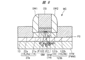
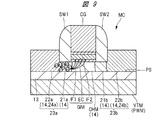
図7および図8は、比較例の半導体装置の要部断面図である。図9および図10は、実施の形態1の半導体装置の要部断面図である。図7および図9は、メモリセルMCの書き込み動作の際の電荷の挙動を模式的に示している。図8および図10は、メモリセルMCの消去動作の際の電荷の挙動を模式的に示している。なお、図7〜図10では、メモリセルMCの周辺を拡大して示し、図3に示したシリサイド膜SIL、層間絶縁膜IL1および層間絶縁膜IL1よりも上方の部分の図示を省略している。また、図7〜図10では、電子を「e-」と標記し、正孔を「h+」と表記している。 7 and 8 are cross-sectional views of main parts of a semiconductor device of a comparative example. 9 and 10 are cross-sectional views of main parts of the semiconductor device of the first embodiment. 7 and 9 schematically show the behavior of charge during the write operation of the memory cell MC. 8 and 10 schematically show the behavior of charges during the erase operation of the memory cell MC. 7 to 10 show the periphery of the memory cell MC in an enlarged manner, and the illustration of the portion above the silicide film SIL, the interlayer insulating film IL1, and the interlayer insulating film IL1 shown in FIG. 3 is omitted. . In FIGS. 7 to 10, electrons are denoted as “e − ” and holes are denoted as “h + ”.
図11は、比較例の半導体装置および実施の形態1の半導体装置において、正孔の密度の深さ方向の位置依存性を示すグラフである。図11は、データを消去するための電圧を印加した直後の、ゲート電極CG、ゲート絶縁膜GIM、チャネル領域CHM、BOX層13、ならびに、半導体領域VTMを含めたp型ウェルPWMの各々における正孔の密度を、TCAD(Technology Computer-Aided Design)シミュレーションにより計算した結果である。なお、本実施の形態1の計算において、p型の半導体領域23bにおけるp型の不純物濃度が、1×1020cm-3以上になるような条件で、計算を行っている。また、比較例の計算においては、p型の半導体領域23bに代え、n型の半導体領域123bを有すること以外の条件を等しくして、計算を行っている。
FIG. 11 is a graph showing the position dependency of the hole density in the depth direction in the semiconductor device of the comparative example and the semiconductor device of the first embodiment. FIG. 11 shows the positive electrode in each of the p-type well PWM including the gate electrode CG, the gate insulating film GIM, the channel region CHM, the
比較例の半導体装置は、メモリセルMCに含まれるソース領域およびドレイン領域に相当する2つの半導体領域のいずれもn型の半導体領域である点で、実施の形態1の半導体装置と異なる。 The semiconductor device of the comparative example is different from the semiconductor device of the first embodiment in that both of the two semiconductor regions corresponding to the source region and the drain region included in the memory cell MC are n-type semiconductor regions.
図7に示すように、メモリセルMCにおいて、サイドウォールスペーサSW2下に位置する部分のSOI層14には、p-型半導体領域21bに代え、n-型半導体領域121bが形成されている。また、平面視において、n-型半導体領域121bを挟んでゲート電極CGと反対側に位置する部分のSOI層14には、n+型半導体領域122bが形成されている。そのため、比較例では、メモリ形成領域MRで、平面視において、ゲート電極CGに対して一方の側と反対側(図7中右側)に位置する部分のSOI層14には、n-型半導体領域121bと、n+型半導体領域122bと、を含むn型の半導体領域123bが形成されている。
As shown in FIG. 7, in the memory cell MC, an n −
比較例の半導体装置においても、図4を用いて説明した方法と同様の方法により、メモリセルMCにデータを書き込む場合を考える。このような場合、メモリセルMCにデータを書き込む際に、n型の半導体領域23aおよび123b(図4のp型の半導体領域23bに相当)のいずれに印加される電圧よりも高い電圧が、ゲート電極CGに印加される。このとき、n型の半導体領域23aおよび123bのいずれからも、電荷蓄積膜ECに、電子が、例えばFNトンネルにより注入される。このn型の半導体領域23aおよび123bから電荷蓄積膜ECに電子が注入される速度は、速い。
Also in the semiconductor device of the comparative example, consider a case where data is written to the memory cell MC by the same method as described with reference to FIG. In such a case, when data is written to the memory cell MC, a voltage higher than the voltage applied to any of the n-
一方、比較例の半導体装置においても、図5を用いて説明した方法と同様の方法により、メモリセルMCのデータを消去する場合を考える。このような場合、メモリセルMCのデータを消去する際に、n型の半導体領域23aおよび123b(図4の半導体領域23bに相当)のいずれに印加される電圧よりも低い電圧がゲート電極CGに印加される。このとき、チャネル領域CHMまたはp型ウェルPWMから、電荷蓄積膜ECに、正孔が、例えばFNトンネルにより注入される。
On the other hand, also in the semiconductor device of the comparative example, consider a case where data in the memory cell MC is erased by the same method as that described with reference to FIG. In such a case, when erasing data in the memory cell MC, a voltage lower than the voltage applied to either of the n-
ところが、チャネル領域CHMにおけるp型の不純物濃度は、p型ウェルPWMにおけるp型の不純物濃度に比べても低い。そのため、チャネル領域CHMから電荷蓄積膜ECに注入される正孔の数は、p型ウェルPWMから電荷蓄積膜ECに注入される正孔の数に比べ、極めて少ない。また、p型ウェルPWMから電荷蓄積膜ECに正孔を注入する前に、例えばBOX層13を挟んで形成されている容量素子に電荷が蓄積、すなわち充電される必要があるので、p型ウェルPWMから電荷蓄積膜ECに正孔が注入される速度は、チャネル領域CHMから電荷蓄積膜ECに正孔が注入される速度に比べて、遅い。
However, the p-type impurity concentration in the channel region CHM is lower than the p-type impurity concentration in the p-type well PWM. Therefore, the number of holes injected from the channel region CHM into the charge storage film EC is extremely smaller than the number of holes injected from the p-type well PWM into the charge storage film EC. Further, before injecting holes from the p-type well PWM into the charge storage film EC, for example, charge needs to be accumulated, that is, charged in a capacitive element formed with the
すなわち、比較例の半導体装置では、データの書き込み速度は速いものの、データの消去速度が遅くなり、半導体装置の性能を向上させることができない。 That is, in the semiconductor device of the comparative example, although the data writing speed is high, the data erasing speed is slow, and the performance of the semiconductor device cannot be improved.
一方、本実施の形態1の半導体装置では、図9および図10に示すように、メモリセルMCに含まれるソース領域およびドレイン領域に相当する2つの半導体領域のうち、一方がn型の半導体領域23aであり、他方はp型の半導体領域23bである。
On the other hand, in the semiconductor device of the first embodiment, as shown in FIGS. 9 and 10, one of the two semiconductor regions corresponding to the source region and the drain region included in the memory cell MC is an n-type semiconductor region. The other is a p-
本実施の形態1の半導体装置においては、メモリセルMCにデータを書き込む際に、n型の半導体領域23aおよびp型の半導体領域23bのいずれに印加される電圧よりも高い電圧が、ゲート電極CGに印加される。このとき、図9に示すように、n型の半導体領域23aから、電荷蓄積膜ECに、電子が、例えばFNトンネルにより注入される。すなわち、本実施の形態1の半導体装置においては、n型の半導体領域23aから電荷蓄積膜ECに電子が注入されることにより、メモリセルMCにデータが書き込まれる。このn型の半導体領域23aから電荷蓄積膜ECに電子が注入される速度は、速い。
In the semiconductor device of the first embodiment, when data is written to the memory cell MC, a voltage higher than the voltage applied to either the n-
また、本実施の形態1の半導体装置においては、メモリセルMCのデータを消去する際に、n型の半導体領域23aおよびおよびp型の半導体領域23bのいずれに印加される電圧よりも低い電圧がゲート電極CGに印加される。このとき、図10に示すように、p型の半導体領域23bから、電荷蓄積膜ECに、正孔が、例えばFNトンネルにより注入される。すなわち、本実施の形態1の半導体装置においては、p型の半導体領域23bから電荷蓄積膜ECに正孔が注入されることにより、メモリセルMCに記憶されたデータが消去される。
In the semiconductor device of the first embodiment, when erasing data in the memory cell MC, a voltage lower than the voltage applied to either the n-
p型の半導体領域23bにおけるp型の不純物濃度は、チャネル領域CHMにおけるp型の不純物濃度よりも高い。そのため、p型の半導体領域23bから電荷蓄積膜ECに注入される正孔の数は、チャネル領域CHMから電荷蓄積膜ECに注入される正孔の数に比べ、極めて多い。
The p-type impurity concentration in the p-
したがって、p型ウェルPWMから電荷蓄積膜ECに正孔が注入される必要がない。また、p型の半導体領域23bから電荷蓄積膜ECに正孔が注入される速度は、チャネル領域CHMおよびp型ウェルPWMから電荷蓄積膜ECに正孔が注入される速度に比べ、速い。
Therefore, it is not necessary to inject holes from the p-type well PWM into the charge storage film EC. Further, the rate at which holes are injected from the p-
図11のグラフからも、データを消去するための電圧を印加した直後に、実施の形態1でのチャネル領域CHMにおける正孔の密度が、比較例でのチャネル領域CHMにおけるに正孔の密度よりも高くなっていることが分かる。また、データを消去するための電圧を印加した直後に、実施の形態1での電荷蓄積膜EC(図11ではゲート絶縁膜GIMとして表記)における正孔の密度が、比較例での電荷蓄積膜EC(図11ではゲート絶縁膜GIMとして表記)における正孔の密度よりも高くなっていることが分かる。これらのことから、図11に示すデータは、本実施の形態1において、比較例に比べ、電荷蓄積膜ECに注入される正孔の数が多いことを裏付けるものである。 Also from the graph of FIG. 11, immediately after applying the voltage for erasing data, the hole density in the channel region CHM in the first embodiment is higher than the hole density in the channel region CHM in the comparative example. It can be seen that is also high. Immediately after the voltage for erasing data is applied, the hole density in the charge storage film EC (shown as the gate insulating film GIM in FIG. 11) in the first embodiment is equal to the charge storage film in the comparative example. It can be seen that the density of holes in the EC (shown as the gate insulating film GIM in FIG. 11) is higher. For these reasons, the data shown in FIG. 11 confirms that the number of holes injected into the charge storage film EC is larger in the first embodiment than in the comparative example.
<本実施の形態の主要な特徴と効果>
以上説明したように、本実施の形態1の半導体装置では、メモリ形成領域MRで、平面視において、ゲート電極CGに対して一方の側に位置する部分のSOI層14には、n-型半導体領域21aと、n+型半導体領域22aと、を含むn型の半導体領域23aが形成されている。また、本実施の形態1の半導体装置では、メモリ形成領域MRで、平面視において、ゲート電極CGに対して一方の側と反対側に位置する部分のSOI層14には、p-型半導体領域21bと、p+型半導体領域22bと、を含むp型の半導体領域23bが形成されている。
<Main features and effects of the present embodiment>
As described above, in the semiconductor device of the first embodiment, in the memory formation region MR, the
そのため、本実施の形態1の半導体装置では、メモリセルMCのデータを消去する際に、p型の半導体領域23bから電荷蓄積膜ECに正孔が注入される速度が速いので、データの消去速度が速くなり、半導体装置の性能を向上させることができる。
Therefore, in the semiconductor device according to the first embodiment, when erasing data in the memory cell MC, the rate at which holes are injected from the p-
好適には、n型の半導体領域23aにおけるn型の不純物濃度は、p型の半導体領域23bにおけるp型の不純物濃度よりも高い。
Preferably, the n-type impurity concentration in the n-
本実施の形態1におけるメモリセルMCでは、チャネル領域CHMがp型の半導体領域である場合、n型の半導体領域23aにおけるn型の不純物濃度を高くした方が、p型の半導体領域23bにおけるp型の不純物濃度を高くした場合よりも、n型の半導体領域23aとp型の半導体領域23bとの間で流れる電流が大きくなる。そして、n型の半導体領域23aとp型の半導体領域23bとの間で流れる電流が大きくなると、読み出し電圧を低くすることができるので、半導体装置の性能を向上させることができる。
In the memory cell MC according to the first embodiment, when the channel region CHM is a p-type semiconductor region, the n-type impurity concentration in the n-
これは、チャネル領域CHMがp型の半導体領域である場合、例えば、n型の半導体領域23aとp型の半導体領域23bとの間を流れる電流の大きさが、p型の半導体領域であるチャネル領域CHMとn型の半導体領域23aとの間のpn接合を流れる電流の大きさの影響を受けるためとも考えられる。このような場合、p型の半導体領域23bにおけるp型の不純物濃度を高くする場合よりも、n型の半導体領域23aにおけるn型の不純物濃度を高くした場合に、pn接合を流れる電流の大きさをより大きくすることができると考えられる。
This is because, when the channel region CHM is a p-type semiconductor region, for example, the magnitude of the current flowing between the n-
具体的には、n+型半導体領域22aにおけるn型の不純物濃度を、p+型半導体領域22bにおけるp型の不純物濃度よりも高くすることができる。
Specifically, the n-type impurity concentration in the n + -
好適には、メモリセルMCに記憶されたデータを読み出す際に、p型の半導体領域23bには、n型の半導体領域23aに印加される電圧よりも高い電圧が印加される。すなわち、メモリセルMCをnチャネル型のMISFETに類似したものと捉えた場合、p型の半導体領域23bをnチャネル型のMISFETのドレイン領域とし、n型の半導体領域23aをnチャネル型のMISFETのソース領域として読み出し動作を行う。
Preferably, when reading data stored in the memory cell MC, a voltage higher than a voltage applied to the n-
一方、p型の半導体領域23bをnチャネル型のMISFETのソース領域とし、n型の半導体領域23aをnチャネル型のMISFETのドレイン領域とした場合でも、p型の半導体領域であるチャネル領域CHMと、n型の半導体領域23aとの間のpn接合に順方向の電圧が印加されれば読み出し動作は可能である。このような場合、n型の半導体領域23aに、p型の半導体領域23bに印加される電圧よりも低い電圧を印加すればよい。
On the other hand, even when the p-
しかし、通常のnチャネル型のMISFETにおいては、ソース領域に0Vを印加し、ドレイン領域に正の電圧を印加する、すなわちソース線SL1(図6参照)の電位を0Vとし、データ線DL1(図6参照)の電位を正の電位とする場合が一般的である。このことを考慮すると、データを読み出す際に、p型の半導体領域23bには、n型の半導体領域23aに印加される電圧よりも高い電圧が印加されることが好ましい。そして、このような場合、メモリセルMCが形成されたメモリ形成領域MRと、それ以外の領域との間で、ソース領域に接続される配線同士を電気的に接続するか、または、ドレイン領域に接続される配線同士を電気的に接続することができ、半導体装置の設計を容易にすることができる。
However, in a normal n-channel MISFET, 0 V is applied to the source region and a positive voltage is applied to the drain region, that is, the potential of the source line SL1 (see FIG. 6) is set to 0 V, and the data line DL1 (FIG. 6) is generally a positive potential. Considering this, when reading data, it is preferable that a voltage higher than the voltage applied to the n-
なお、本実施の形態1におけるメモリセルMCに含まれる各半導体領域の導電型を一括して逆の導電型にしてもよい。このような場合には、消去動作の際に、正孔に代えて電子を注入することになるが、その電子を注入する速度を速くすることができ、半導体装置の性能を向上させることができる。 Note that the conductivity type of each semiconductor region included in the memory cell MC in the first embodiment may be collectively changed to the opposite conductivity type. In such a case, electrons are injected instead of holes in the erasing operation, but the speed of injecting the electrons can be increased and the performance of the semiconductor device can be improved. .
また、本実施の形態1におけるメモリセルMCのゲート絶縁膜GIMが、電荷蓄積膜ECに代えて例えば金属膜などの導電膜を有し、かつ、その導電膜が電気的に浮遊した状態であってもよい。すなわち、本実施の形態1におけるメモリセルMCが、電荷蓄積部としてSONOS膜を有するものではなく、フローティングゲートを有するものであってもよい。 In addition, the gate insulating film GIM of the memory cell MC in the first embodiment has a conductive film such as a metal film instead of the charge storage film EC, and the conductive film is in an electrically floating state. May be. In other words, the memory cell MC according to the first embodiment may have a floating gate instead of the SONOS film as the charge storage portion.
<実施の形態1の半導体装置の変形例>
図12は、実施の形態1の変形例の半導体装置の要部断面図である。
<Modification of Semiconductor Device of First Embodiment>
FIG. 12 is a fragmentary cross-sectional view of a semiconductor device according to a modification of the first embodiment.
図12に示すように、隣り合う2つのメモリセルMCとしてのメモリセルMC1およびMC2が、メモリセルMC1およびMC2の各々に含まれるn型の半導体領域23a同士が隣り合うように配置され、配線ML1としての配線ML11が、ソース線として共有されていてもよい。すなわち、配線ML11は、プラグPGおよびシリサイド膜SILを介してメモリセルMC1のn型の半導体領域23aと電気的に接続され、かつ、プラグPGおよびシリサイド膜SILを介してメモリセルMC2のn型の半導体領域23aと電気的に接続されていてもよい。これにより、半導体チップの面積を低減し、配線ML1の数を低減することができる。
As shown in FIG. 12, memory cells MC1 and MC2 as two adjacent memory cells MC are arranged such that n-
また、図12に示すように、隣り合う2つのメモリセルMCとしてのメモリセルMC1およびMC2の各々に含まれるp型ウェルPWMが、接触せず、分離されていてもよい。これにより、例えばメモリセルMC1およびMC2の各々に含まれるp型ウェルPWMに印加される電圧を、個別に制御することができる。 Further, as shown in FIG. 12, the p-type well PWM included in each of the memory cells MC1 and MC2 as two adjacent memory cells MC may be separated without being in contact with each other. Thereby, for example, the voltage applied to the p-type well PWM included in each of the memory cells MC1 and MC2 can be individually controlled.
<半導体装置の製造方法>
次に、本実施の形態1の半導体装置の製造方法について説明する。
<Method for Manufacturing Semiconductor Device>
Next, a method for manufacturing the semiconductor device according to the first embodiment will be described.
図13および図14は、実施の形態1の半導体装置の製造工程の一部を示すプロセスフロー図である。図15〜図26は、実施の形態1の半導体装置の製造工程中の要部断面図である。図15〜図26には、メモリ形成領域MRおよび主回路形成領域ARの要部断面図が示されている。 13 and 14 are process flow diagrams showing a part of the manufacturing process of the semiconductor device of the first embodiment. 15 to 26 are main-portion cross-sectional views during the manufacturing process of the semiconductor device of First Embodiment. 15 to 26 are cross-sectional views of main parts of the memory formation region MR and the main circuit formation region AR.
本実施の形態1においては、メモリ形成領域MRにnチャネル型のMISFETに類似した構造を有するメモリセルMC(図26参照)を形成する場合について説明するが、導電型を逆にしてpチャネル型のMISFETに類似した構造を有するメモリセルMCを形成することもできる(以下の実施の形態においても同様)。 In the first embodiment, a case where a memory cell MC (see FIG. 26) having a structure similar to an n-channel type MISFET is formed in the memory formation region MR will be described. A memory cell MC having a structure similar to that of MISFET can also be formed (the same applies to the following embodiments).
本実施の形態1においては、主回路形成領域ARの低耐圧MISFET形成領域AR1に、nチャネル型のMISFET7a(図25参照)を形成し、主回路形成領域ARの低耐圧MISFET形成領域AR2に、pチャネル型のMISFET7b(図26参照)を形成する場合について説明する。なお、主回路形成領域ARのうち低耐圧MISFET形成領域AR1の外部の領域を領域AR3とし、主回路形成領域ARのうち低耐圧MISFET形成領域AR2の外部の領域を領域AR4とする。
In the first embodiment, an n-
まず、図15に示すように、SOI基板SBを用意、すなわち準備する(図13のステップS1)。このステップS1では、基体SSと、メモリ形成領域MR、ならびに、低耐圧MISFET形成領域AR1およびAR2で、基体SS上に形成されたBOX層13と、BOX層13上に形成されたSOI層14と、を有する、半導体基板としてのSOI基板SBを用意する。
First, as shown in FIG. 15, an SOI substrate SB is prepared, that is, prepared (step S1 in FIG. 13). In this step S1, the
基体SSは、例えばシリコン(Si)基板からなり、好適には、シリコン単結晶基板からなる。BOX層13は、例えば酸化シリコン膜からなる。BOX層13の厚さは、例えば10〜40nm程度である。SOI層14は、例えばシリコン単結晶層からなる。SOI層14の厚さは、例えば10〜20nm程度である。
The base body SS is made of, for example, a silicon (Si) substrate, preferably a silicon single crystal substrate. The
次に、図15に示すように、素子分離領域SRを形成する(図13のステップS2)。このステップS2では、例えば、STI(Shallow Trench Isolation)法を用いて素子分離領域SRを形成する。 Next, as shown in FIG. 15, an element isolation region SR is formed (step S2 in FIG. 13). In this step S2, the element isolation region SR is formed using, for example, an STI (Shallow Trench Isolation) method.
このSTI法では、まず、SOI基板SBにフォトリソグラフィ技術およびエッチング技術を使用して素子分離溝を形成する。そして、素子分離溝を埋め込むようにSOI基板SB上に、例えば酸化シリコン膜からなる絶縁膜を形成し、その後、化学的機械的研磨(Chemical Mechanical Polishing:CMP)法により、SOI基板SB上に形成された不要な絶縁膜を除去する。これにより、素子分離溝内にだけ絶縁膜を埋め込んだ素子分離領域SRを形成することができる。 In this STI method, first, an element isolation trench is formed in an SOI substrate SB using a photolithography technique and an etching technique. Then, an insulating film made of, for example, a silicon oxide film is formed on the SOI substrate SB so as to fill the element isolation trench, and then formed on the SOI substrate SB by a chemical mechanical polishing (CMP) method. The unnecessary insulating film is removed. Thereby, the element isolation region SR in which the insulating film is embedded only in the element isolation trench can be formed.
このようにして、素子分離領域SRを形成することにより、素子分離領域SRによって、メモリ形成領域MRと主回路形成領域ARとが区画され、主回路形成領域ARは、低耐圧MISFET形成領域AR1と低耐圧MISFET形成領域AR2と領域AR3と領域AR4とに区画される。 By forming the element isolation region SR in this manner, the memory isolation region MR and the main circuit formation region AR are partitioned by the element isolation region SR. The main circuit formation region AR is separated from the low breakdown voltage MISFET formation region AR1. The low breakdown voltage MISFET formation region AR2, the region AR3, and the region AR4 are partitioned.
次に、図15に示すように、犠牲酸化膜SO1を形成する(図13のステップS3)。このステップS3では、メモリ形成領域MR、ならびに、低耐圧MISFET形成領域AR1およびAR2で、SOI層14上に、犠牲酸化膜SO1を、例えば熱酸化法などにより形成する。このとき、メモリ形成領域MR、ならびに、低耐圧MISFET形成領域AR1およびAR2で、SOI層14上に、犠牲酸化膜SO1が形成される。犠牲酸化膜SO1は、例えば酸化シリコン膜からなる。なお、犠牲酸化膜SO1は、領域AR3およびAR4でも、SOI層14上に形成される。
Next, as shown in FIG. 15, a sacrificial oxide film SO1 is formed (step S3 in FIG. 13). In this step S3, a sacrificial oxide film SO1 is formed on the
犠牲酸化膜SO1を形成することにより、後述するステップS4において、p型ウェルPWMおよびPWL、ならびに、n型ウェルNWL(後述する図16参照)を形成する際に、SOI層14に損傷が加えられることを防止することができる。
By forming the sacrificial oxide film SO1, the
次に、図16に示すように、p型ウェルPWMおよびPWL、ならびに、n型ウェルNWLを形成する(図13のステップS4)。 Next, as shown in FIG. 16, p-type wells PWM and PWL and n-type well NWL are formed (step S4 in FIG. 13).
このステップS4では、まず、低耐圧MISFET形成領域AR1およびAR2を覆い、かつ、メモリ形成領域MRを露出させるように、レジスト膜(図示は省略)をパターニングする。そして、パターニングされたレジスト膜(図示は省略)をマスクにしたイオン注入法により、例えばホウ素(B)などのp型の不純物を、基体SSに導入する。 In this step S4, first, a resist film (not shown) is patterned so as to cover the low breakdown voltage MISFET formation regions AR1 and AR2 and to expose the memory formation region MR. Then, a p-type impurity such as boron (B) is introduced into the substrate SS by an ion implantation method using a patterned resist film (not shown) as a mask.
これにより、メモリ形成領域MRで、基体SSの主面としての上面PS側に、p型ウェルPWMを形成する。p型ウェルPWMにおけるp型の不純物濃度が、例えば5×10¹⁷〜5×1018cm-3程度になるように、イオン注入の際の注入条件が調整される。このとき、メモリ形成領域MRで、SOI層14上に犠牲酸化膜SO1が形成されているため、イオン注入法によりp型ウェルPWMを形成する際に、p型ウェルPWMの上面に損傷が加えられることを防止することができる。
Thus, the p-type well PWM is formed on the upper surface PS side as the main surface of the base body SS in the memory formation region MR. The implantation conditions during ion implantation are adjusted so that the p-type impurity concentration in the p-type well PWM is, for example, about 5 × 10 17 to 5 × 10 18 cm −3 . At this time, since the sacrificial oxide film SO1 is formed on the
このステップS4では、また、メモリ形成領域MRおよび低耐圧MISFET形成領域AR2を覆い、かつ、低耐圧MISFET形成領域AR1を露出させるように、パターニングされたレジスト膜(図示は省略)をマスクにしたイオン注入法により、例えばホウ素(B)などのp型の不純物を、基体SSに導入する。 In this step S4, ions are formed using a resist film (not shown) patterned to cover the memory formation region MR and the low breakdown voltage MISFET formation region AR2 and expose the low breakdown voltage MISFET formation region AR1. A p-type impurity such as boron (B) is introduced into the substrate SS by an implantation method.
これにより、低耐圧MISFET形成領域AR1で、基体SSの上面PS側に、p型ウェルPWLを形成する。p型ウェルPWLにおけるp型の不純物濃度が、例えば5×10¹⁷〜5×1018cm-3程度になるように、イオン注入の際の注入条件が調整される。このとき、低耐圧MISFET形成領域AR1で、SOI層14上に犠牲酸化膜SO1が形成されているため、イオン注入法によりp型ウェルPWLを形成する際に、SOI層14に損傷が加えられることを防止することができる。
Thereby, the p-type well PWL is formed on the upper surface PS side of the base SS in the low breakdown voltage MISFET formation region AR1. The implantation conditions for ion implantation are adjusted so that the p-type impurity concentration in the p-type well PWL is, for example, about 5 × 10 17 to 5 × 10 18 cm −3 . At this time, since the sacrificial oxide film SO1 is formed on the
なお、p型ウェルPWLは、低耐圧MISFET形成領域AR1の外部の領域AR3でも、基体SSの上面PS側に形成される。 The p-type well PWL is also formed on the upper surface PS side of the base SS in the region AR3 outside the low breakdown voltage MISFET formation region AR1.
このステップS4では、また、メモリ形成領域MRおよび低耐圧MISFET形成領域AR1を覆い、かつ、低耐圧MISFET形成領域AR2を露出させるように、レジスト膜(図示は省略)をパターニングする。そして、パターニングされたレジスト膜(図示は省略)をマスクにしたイオン注入法により、例えばリン(P)またはヒ素(As)などのn型の不純物を、基体SSに導入する。 In this step S4, a resist film (not shown) is patterned so as to cover the memory formation region MR and the low breakdown voltage MISFET formation region AR1 and expose the low breakdown voltage MISFET formation region AR2. Then, an n-type impurity such as phosphorus (P) or arsenic (As) is introduced into the substrate SS by an ion implantation method using a patterned resist film (not shown) as a mask.
これにより、低耐圧MISFET形成領域AR2で、基体SSの上面PS側に、n型ウェルNWLを形成する。n型ウェルNWLにおけるn型の不純物濃度が、例えば5×10¹⁷〜5×1018cm-3程度になるように、イオン注入の際の注入条件が調整される。このとき、低耐圧MISFET形成領域AR2で、SOI層14上に犠牲酸化膜SO1が形成されているため、イオン注入法によりn型ウェルNWLを形成する際に、SOI層14に損傷が加えられることを防止することができる。
Thereby, the n-type well NWL is formed on the upper surface PS side of the base SS in the low breakdown voltage MISFET formation region AR2. The implantation conditions for ion implantation are adjusted so that the n-type impurity concentration in the n-type well NWL is, for example, about 5 × 10 17 to 5 × 10 18 cm −3 . At this time, since the sacrificial oxide film SO1 is formed on the
なお、n型ウェルNWLは、低耐圧MISFET形成領域AR2の外部の領域AR4でも、基体SSの上面PS側に形成される。 Note that the n-type well NWL is also formed on the upper surface PS side of the base SS in the region AR4 outside the low breakdown voltage MISFET formation region AR2.
次に、図17に示すように、半導体領域VTM、VT1およびVT2を形成する(図13のステップS5)。 Next, as shown in FIG. 17, semiconductor regions VTM, VT1, and VT2 are formed (step S5 in FIG. 13).
このステップS5では、低耐圧MISFET形成領域AR1およびAR2を覆い、かつ、メモリ形成領域MRを露出させるように、レジスト膜(図示は省略)をパターニングする。そして、パターニングされたレジスト膜(図示は省略)をマスクにしたイオン注入法により、例えばホウ素(B)などのp型の不純物を、p型ウェルPWMの上層部に導入する。 In this step S5, a resist film (not shown) is patterned so as to cover the low breakdown voltage MISFET formation regions AR1 and AR2 and expose the memory formation region MR. Then, a p-type impurity such as boron (B) is introduced into the upper layer of the p-type well PWM by an ion implantation method using a patterned resist film (not shown) as a mask.
これにより、メモリ形成領域MRで、p型ウェルPWMの上層部に、半導体領域VTMを形成する。半導体領域VTMにおけるp型の不純物濃度が、例えば5×10¹⁷〜5×1018cm-3程度で、かつ、p型ウェルPWMにおけるp型の不純物濃度よりも高くなるように、イオン注入の際の注入条件が調整される。このとき、メモリ形成領域MRで、SOI層14上に犠牲酸化膜SO1が形成されているため、イオン注入法により半導体領域VTMを形成する際に、SOI層14に損傷が加えられることを防止することができる。
As a result, the semiconductor region VTM is formed in the upper layer portion of the p-type well PWM in the memory formation region MR. During ion implantation, the p-type impurity concentration in the semiconductor region VTM is, for example, about 5 × 10 17 to 5 × 10 18 cm −3 and higher than the p-type impurity concentration in the p-type well PWM. The injection conditions are adjusted. At this time, since the sacrificial oxide film SO1 is formed on the
このステップS5では、また、メモリ形成領域MRおよび低耐圧MISFET形成領域AR2を覆い、かつ、低耐圧MISFET形成領域AR1を露出させるように、レジスト膜(図示は省略)をパターニングする。そして、パターニングされたレジスト膜(図示は省略)をマスクにしたイオン注入法により、例えばホウ素(B)などのp型の不純物を、p型ウェルPWLの上層部に導入する。 In step S5, a resist film (not shown) is patterned so as to cover the memory formation region MR and the low breakdown voltage MISFET formation region AR2 and expose the low breakdown voltage MISFET formation region AR1. Then, a p-type impurity such as boron (B) is introduced into the upper layer portion of the p-type well PWL by an ion implantation method using a patterned resist film (not shown) as a mask.
これにより、低耐圧MISFET形成領域AR1で、p型ウェルPWLの上層部に、半導体領域VT1を形成する。半導体領域VT1におけるp型の不純物濃度が、例えば5×10¹⁷〜5×1018cm-3程度で、かつ、p型ウェルPWLにおけるp型の不純物濃度よりも高くなるように、イオン注入の際の注入条件が調整される。このとき、低耐圧MISFET形成領域AR1で、SOI層14上に犠牲酸化膜SO1が形成されているため、イオン注入法により半導体領域VT1を形成する際に、SOI層14に損傷が加えられることを防止することができる。
Thus, the semiconductor region VT1 is formed in the upper layer portion of the p-type well PWL in the low breakdown voltage MISFET formation region AR1. During the ion implantation, the p-type impurity concentration in the semiconductor region VT1 is, for example, about 5 × 10 17 to 5 × 10 18 cm −3 and higher than the p-type impurity concentration in the p-type well PWL. The injection conditions are adjusted. At this time, since the sacrificial oxide film SO1 is formed on the
なお、半導体領域VT1は、低耐圧MISFET形成領域AR1の外部の領域AR3でも、p型ウェルPWLの上層部に形成される。 The semiconductor region VT1 is also formed in the upper layer portion of the p-type well PWL in the region AR3 outside the low breakdown voltage MISFET formation region AR1.
このステップS5では、また、メモリ形成領域MRおよび低耐圧MISFET形成領域AR1を覆い、かつ、低耐圧MISFET形成領域AR2を露出させるように、レジスト膜(図示は省略)をパターニングする。そして、パターニングされたレジスト膜(図示は省略)をマスクにしたイオン注入法により、例えばリン(P)またはヒ素(As)などのn型の不純物を、n型ウェルNWLの上層部に導入する。 In this step S5, a resist film (not shown) is patterned so as to cover the memory formation region MR and the low breakdown voltage MISFET formation region AR1 and expose the low breakdown voltage MISFET formation region AR2. Then, an n-type impurity such as phosphorus (P) or arsenic (As) is introduced into the upper layer of the n-type well NWL by an ion implantation method using a patterned resist film (not shown) as a mask.
これにより、低耐圧MISFET形成領域AR2で、n型ウェルNWLの上層部に、半導体領域VT2を形成する。半導体領域VT2におけるn型の不純物濃度が、例えば5×10¹⁷〜5×1018cm-3程度で、かつ、n型ウェルNWLにおけるn型の不純物濃度よりも高くなるように、イオン注入の際の注入条件が調整される。このとき、低耐圧MISFET形成領域AR2で、SOI層14上に犠牲酸化膜SO1が形成されているため、イオン注入法により半導体領域VT2を形成する際に、SOI層14に損傷が加えられることを防止することができる。
Thereby, the semiconductor region VT2 is formed in the upper layer portion of the n-type well NWL in the low breakdown voltage MISFET formation region AR2. During the ion implantation, the n-type impurity concentration in the semiconductor region VT2 is, for example, about 5 × 10 17 to 5 × 10 18 cm −3 and higher than the n-type impurity concentration in the n-type well NWL. The injection conditions are adjusted. At this time, since the sacrificial oxide film SO1 is formed on the
なお、半導体領域VT2は、低耐圧MISFET形成領域AR2の外部の領域AR4でも、n型ウェルNWLの上層部に形成される。 The semiconductor region VT2 is also formed in the upper layer portion of the n-type well NWL in the region AR4 outside the low breakdown voltage MISFET formation region AR2.
このステップS5では、次に、図17に示すように、メモリ形成領域MR、ならびに、低耐圧MISFET形成領域AR1およびAR2で、SOI層14上に形成されている犠牲酸化膜SO1を、例えばフッ酸(HF)を用いたウェットエッチングにより、除去する。
In this step S5, next, as shown in FIG. 17, the sacrificial oxide film SO1 formed on the
このステップS5では、次に、図17に示すように、開口部OP1およびOP2を形成する。すなわち、領域AR3で、レジスト膜をマスクとした異方性ドライエッチング法により、SOI層14の一部を除去し、続いてウェットエッチング法によりBOX層13を除去することにより、SOI層14およびBOX層13を貫通して半導体領域VT1に達する開口部OP1を形成する。また、領域AR4で、レジスト膜をマスクとした異方性ドライエッチング法により、SOI層14の一部を除去し、続いてウェットエッチング法によりBOX層13を除去することにより、SOI層14およびBOX層13を貫通して半導体領域VT2に達する開口部OP2を形成する。開口部OP1は、p型ウェルPWLとの電気的接触を確保するために形成され、開口部OP2は、n型ウェルNWLとの電気的接触を確保するために形成する。
In this step S5, next, as shown in FIG. 17, openings OP1 and OP2 are formed. That is, in the region AR3, a part of the
次に、図18に示すように、絶縁膜IFGおよびIS1を形成する(図4のステップS6)。 Next, as shown in FIG. 18, insulating films IFG and IS1 are formed (step S6 in FIG. 4).
このステップS6では、まず、図18に示すように、メモリ形成領域MR、ならびに、低耐圧MISFET形成領域AR1およびAR2で、SOI層14上に、犠牲酸化膜SO2を、例えば熱酸化法などにより形成する。
In step S6, first, as shown in FIG. 18, a sacrificial oxide film SO2 is formed on the
このとき、メモリ形成領域MR、ならびに、低耐圧MISFET形成領域AR1およびAR2で、SOI層14上に、犠牲酸化膜SO2が形成される。犠牲酸化膜SO2は、例えば酸化シリコン膜からなる。なお、犠牲酸化膜SO2は、領域AR3でも、半導体領域VT1上に形成され、領域AR4でも、半導体領域VT2上に形成される。
At this time, a sacrificial oxide film SO2 is formed on the
このステップS6では、次に、図18に示すように、レジスト膜(図示は省略)をマスクとしたエッチングにより、メモリ形成領域MRに形成されている犠牲酸化膜SO2を除去する。 In this step S6, next, as shown in FIG. 18, the sacrificial oxide film SO2 formed in the memory formation region MR is removed by etching using a resist film (not shown) as a mask.
このステップS6では、次に、図18に示すように、メモリ形成領域MR、ならびに、低耐圧MISFET形成領域AR1およびAR2で、SOI層14上に、犠牲酸化膜SO2を覆う絶縁膜IFGを形成する。具体的には、メモリ形成領域MR、ならびに、低耐圧MISFET形成領域AR1およびAR2で、SOI層14上に、犠牲酸化膜SO2を覆う絶縁膜IF1を形成し、絶縁膜IF1上に電荷蓄積膜ECを形成し、電荷蓄積膜EC上に絶縁膜IF2を形成する。絶縁膜IF1と、電荷蓄積膜ECと、絶縁膜IF2と、により絶縁膜IFGが形成される。絶縁膜IFGは、内部に電荷蓄積部としての電荷蓄積膜ECを有する絶縁膜である。なお、絶縁膜IFGは、領域AR3でも、犠牲酸化膜SO2上に形成され、領域AR4でも、犠牲酸化膜SO2上に形成される。
In this step S6, next, as shown in FIG. 18, an insulating film IFG that covers the sacrificial oxide film SO2 is formed on the
絶縁膜IF1は、例えば酸化シリコン膜からなる。好適には、絶縁膜IF1を、ISSG(In Situ Steam Generation)酸化法により形成することができる。ISSG酸化法は、減圧した熱処理チャンバ内に水素と酸素を直接導入し、例えば800〜1100℃の温度に加熱したシリコンなどからなるSOI層14の表面でラジカル酸化反応をさせることにより、SOI層14の表面に例えば酸化シリコンからなる酸化膜を形成する方法である。ISSG酸化法における酸化力は、ラジカル酸化反応を用いるため、例えば熱酸化法などにおける酸化力に比べて高い。したがって、ISSG酸化法を用いることにより、緻密で良質な膜質の酸化シリコン膜からなる絶縁膜IF1を形成することができる。絶縁膜IF1の厚さは、例えば2nm程度である。
The insulating film IF1 is made of, for example, a silicon oxide film. Preferably, the insulating film IF1 can be formed by an ISSG (In Situ Steam Generation) oxidation method. In the ISSG oxidation method, hydrogen and oxygen are directly introduced into a reduced-pressure heat treatment chamber, and a radical oxidation reaction is performed on the surface of the
電荷蓄積膜ECは、例えば窒化シリコン膜からなる。例えば、電荷蓄積膜ECを、CVD(Chemical Vapor Deposition)法により形成することができる。電荷蓄積膜ECの厚さは、例えば8nm程度である。 The charge storage film EC is made of, for example, a silicon nitride film. For example, the charge storage film EC can be formed by a CVD (Chemical Vapor Deposition) method. The thickness of the charge storage film EC is, for example, about 8 nm.
絶縁膜IF2は、例えば酸化シリコン膜からなる。好適には、絶縁膜IF2を、例えば、HTO(High Temperature Oxide)法により形成することができ、これにより、緻密で良質な膜質の酸化シリコン膜からなる絶縁膜IF2を形成することができる。絶縁膜IF2の厚さは、例えば3nm程度である。 The insulating film IF2 is made of, for example, a silicon oxide film. Preferably, the insulating film IF2 can be formed by, for example, an HTO (High Temperature Oxide) method, whereby the insulating film IF2 made of a dense and high-quality silicon oxide film can be formed. The thickness of the insulating film IF2 is, for example, about 3 nm.
次に、図19に示すように、レジスト膜(図示は省略)をマスクとしたエッチングにより、低耐圧MISFET形成領域AR1およびAR2に形成されている絶縁膜IFGおよび犠牲酸化膜SO2を除去する。このようにして、メモリ形成領域MRで、SOI層14上に、緻密で絶縁耐性に優れた良質な膜質の積層絶縁膜としての絶縁膜IFGを形成することができる。絶縁膜IFGは、ONO(Oxide Nitride Oxide)膜とも称される。なお、領域AR3およびAR4でも、絶縁膜IFGおよび犠牲酸化膜SO2が除去される。
Next, as shown in FIG. 19, the insulating film IFG and the sacrificial oxide film SO2 formed in the low breakdown voltage MISFET formation regions AR1 and AR2 are removed by etching using a resist film (not shown) as a mask. In this manner, in the memory formation region MR, the insulating film IFG can be formed on the
このステップS6では、次に、図19に示すように、低耐圧MISFET形成領域AR1およびAR2で、SOI層14上に、ゲート絶縁膜用の絶縁膜IS1を、例えば熱酸化法などにより形成する。犠牲酸化膜SO1は、例えば酸化シリコン膜からなる。なお、絶縁膜IS1は、領域AR3でも、半導体領域VT1上に形成され、領域AR4でも、半導体領域VT2上に形成される。
In this step S6, next, as shown in FIG. 19, an insulating film IS1 for a gate insulating film is formed on the
次に、図20に示すように、導電膜CF1を形成する(図13のステップS7)。このステップS7では、メモリ形成領域MR、ならびに、低耐圧MISFET形成領域AR1およびAR2で、絶縁膜IFG上に、ゲート電極用の導電膜CF1を形成する。 Next, as shown in FIG. 20, a conductive film CF1 is formed (step S7 in FIG. 13). In step S7, a conductive film CF1 for a gate electrode is formed on the insulating film IFG in the memory formation region MR and the low breakdown voltage MISFET formation regions AR1 and AR2.
好適には、導電膜CF1は、多結晶シリコン膜、すなわちポリシリコン膜からなる。このような導電膜CF1を、CVD法などを用いて形成することができる。導電膜CF1の厚さを、絶縁膜IFGおよびIS1を覆うように十分な程度の厚さとすることができる。また、導電膜CF1の成膜時は導電膜CF1をアモルファスシリコン膜として成膜してから、その後の熱処理でアモルファスシリコン膜を多結晶シリコン膜とすることもできる。 Preferably, the conductive film CF1 is made of a polycrystalline silicon film, that is, a polysilicon film. Such a conductive film CF1 can be formed using a CVD method or the like. The thickness of the conductive film CF1 can be set to a thickness sufficient to cover the insulating films IFG and IS1. Further, when the conductive film CF1 is formed, the conductive film CF1 can be formed as an amorphous silicon film, and then the amorphous silicon film can be converted into a polycrystalline silicon film by a subsequent heat treatment.
好適には、メモリ形成領域MRおよび低耐圧MISFET形成領域AR1では、導電膜CF1に含まれる導電膜CF11として、例えばリン(P)またはヒ素(As)などのn型の不純物を導入したものを用いることができる。また、低耐圧MISFET形成領域AR2では、導電膜CF1に含まれる導電膜CF12として、例えばホウ素(B)などのp型の不純物を導入したものを用いることができる。 Preferably, in the memory formation region MR and the low breakdown voltage MISFET formation region AR1, a conductive film CF11 included in the conductive film CF1 is doped with an n-type impurity such as phosphorus (P) or arsenic (As). be able to. In the low breakdown voltage MISFET formation region AR2, a conductive film CF12 included in the conductive film CF1 can be formed by introducing a p-type impurity such as boron (B).
不純物は、導電膜CF1の成膜時または成膜後に導入することができる。導電膜CF1の成膜時に不純物を導入する場合には、導電膜CF1の成膜用のガスにドーピングガスを含ませることで、不純物が導入された導電膜CF1を成膜することができる。あるいは、シリコン膜の成膜後に不純物を導入する場合には、意図的には不純物を導入せずにシリコン膜を成膜した後に、このシリコン膜に不純物をイオン注入法などで導入することにより、不純物が導入された導電膜CF1を形成することができる。 Impurities can be introduced during or after the formation of the conductive film CF1. In the case of introducing an impurity when forming the conductive film CF1, the conductive film CF1 into which the impurity is introduced can be formed by adding a doping gas to the gas for forming the conductive film CF1. Alternatively, when introducing an impurity after the formation of the silicon film, by intentionally introducing the impurity into the silicon film by ion implantation or the like after forming the silicon film without intentionally introducing the impurity, A conductive film CF1 into which an impurity is introduced can be formed.
次に、図21に示すように、導電膜CF1および絶縁膜IFGをパターニングする(図13のステップS8)。 Next, as shown in FIG. 21, the conductive film CF1 and the insulating film IFG are patterned (step S8 in FIG. 13).
このステップS8では、まず、図21に示すように、導電膜CF1上に、例えば窒化シリコン膜などからなるハードマスク膜HMを形成し、ハードマスク膜HM上にレジスト膜(図示は省略)を塗布した後、フォトリソグラフィ技術およびエッチング技術を使用することにより、ハードマスク膜HMをパターニングする。ハードマスク膜HMは、メモリ形成領域MRのうち、ゲート電極CGを形成する領域に配置された部分の導電膜CF1が、ハードマスク膜HMにより覆われ、メモリ形成領域MRのうち、ゲート電極CGを形成する領域以外の領域に配置された部分の導電膜CF1が、ハードマスク膜HMから露出するように、パターニングされる。また、ハードマスク膜HMは、低耐圧MISFET形成領域AR1およびAR2でも同様に、ゲート電極GE1およびGE2を形成する領域に配置された部分の導電膜CF1が、ハードマスク膜HMにより覆われるように、パターニングされる。 In this step S8, first, as shown in FIG. 21, a hard mask film HM made of, for example, a silicon nitride film is formed on the conductive film CF1, and a resist film (not shown) is applied on the hard mask film HM. After that, the hard mask film HM is patterned by using a photolithography technique and an etching technique. In the hard mask film HM, a portion of the conductive film CF1 arranged in a region where the gate electrode CG is formed in the memory formation region MR is covered with the hard mask film HM, and the gate electrode CG is covered in the memory formation region MR. The portion of the conductive film CF1 disposed in a region other than the region to be formed is patterned so as to be exposed from the hard mask film HM. Similarly, in the hard mask film HM, in the low breakdown voltage MISFET formation regions AR1 and AR2, a portion of the conductive film CF1 disposed in the region where the gate electrodes GE1 and GE2 are formed is covered with the hard mask film HM. Patterned.
このステップS8では、次に、図21に示すように、パターニングされたハードマスク膜HMをマスクとして用いて、導電膜CF1、ならびに、絶縁膜IFGおよびIS1を、例えばドライエッチングなどによりエッチングしてパターニングする。 In this step S8, next, as shown in FIG. 21, using the patterned hard mask film HM as a mask, the conductive film CF1 and the insulating films IFG and IS1 are etched and patterned by, for example, dry etching or the like. To do.
これにより、メモリ形成領域MRで、導電膜CF1からなるゲート電極CGが形成され、ゲート電極CGとSOI層14との間の部分の絶縁膜IFGからなるゲート絶縁膜GIMが形成される。すなわち、ゲート電極CGは、メモリ形成領域MRで、SOI層14上に、ゲート絶縁膜GIMを介して形成される。
Thus, the gate electrode CG made of the conductive film CF1 is formed in the memory formation region MR, and the gate insulating film GIM made of the insulating film IFG in the portion between the gate electrode CG and the
また、低耐圧MISFET形成領域AR1で、SOI層14上に、導電膜CF1からなるゲート電極GE1が形成され、ゲート電極GE1とSOI層14との間の部分の絶縁膜IS1からなるゲート絶縁膜GI1が形成される。すなわち、ゲート電極GE1は、低耐圧MISFET形成領域AR1で、SOI層14上に、ゲート絶縁膜GI1を介して形成される。
Further, in the low breakdown voltage MISFET formation region AR1, the gate electrode GE1 made of the conductive film CF1 is formed on the
また、低耐圧MISFET形成領域AR2で、SOI層14上に、導電膜CF1からなるゲート電極GE2が形成され、ゲート電極GE2とSOI層14との間の部分の絶縁膜IS1からなるゲート絶縁膜GI2が形成される。すなわち、ゲート電極GE2は、低耐圧MISFET形成領域AR2で、SOI層14上に、ゲート絶縁膜GI2を介して形成される。
In the low breakdown voltage MISFET formation region AR2, the gate electrode GE2 made of the conductive film CF1 is formed on the
このように、図18〜図21を用いて説明した工程を行うことにより、SOI層14上に、内部に電荷蓄積膜ECを有するゲート絶縁膜GIMを形成し、ゲート絶縁膜GIM上に、ゲート電極CGを形成することになる。
As described above, by performing the steps described with reference to FIGS. 18 to 21, the gate insulating film GIM having the charge storage film EC inside is formed on the
なお、図18〜図21を用いて説明した工程は一例である。したがって、例えば、メモリ形成領域MRでゲート絶縁膜用の絶縁膜およびゲート電極用の導電膜を形成する工程を、低耐圧MISFET形成領域AR1およびAR2でゲート絶縁膜用の絶縁膜およびゲート電極用の導電膜を形成する工程の前または後に行うなど、各種の方法を用いることができる。 In addition, the process demonstrated using FIGS. 18-21 is an example. Therefore, for example, the process of forming the insulating film for the gate insulating film and the conductive film for the gate electrode in the memory forming region MR is performed in the process for forming the insulating film for the gate insulating film and the gate electrode in the low breakdown voltage MISFET forming regions AR1 and AR2. Various methods such as performing before or after the step of forming the conductive film can be used.
次に、図22に示すように、サイドウォールスペーサSP1、SP2、SP3およびSP4を形成する(図13のステップS9)。 Next, as shown in FIG. 22, sidewall spacers SP1, SP2, SP3 and SP4 are formed (step S9 in FIG. 13).
このステップS9では、まず、図22に示すように、メモリ形成領域MR、低耐圧MISFET形成領域AR1およびAR2で、SOI層14上に、サイドウォールスペーサ用の絶縁膜IS2を形成する。絶縁膜IS2は、例えば窒化シリコン膜からなる。
In this step S9, first, as shown in FIG. 22, an insulating film IS2 for a sidewall spacer is formed on the
このステップS10では、次に、図22に示すように、絶縁膜IS2を、例えば異方性エッチングによりエッチバックする。このようにして、メモリ形成領域MRで、ゲート電極CGの一方の側(図22中左側)の側面に、絶縁膜IS2からなるサイドウォールスペーサSP1を形成し、ゲート電極CGの一方の側と反対側(図22中右側)の側面に、絶縁膜IS2からなるサイドウォールスペーサSP2を形成する。 In this step S10, next, as shown in FIG. 22, the insulating film IS2 is etched back by anisotropic etching, for example. In this way, in the memory formation region MR, the sidewall spacer SP1 made of the insulating film IS2 is formed on the side surface on one side (left side in FIG. 22) of the gate electrode CG, and is opposite to one side of the gate electrode CG. A side wall spacer SP2 made of the insulating film IS2 is formed on the side surface (right side in FIG. 22).
また、低耐圧MISFET形成領域AR1で、ゲート電極GE1の両側面の各々に、絶縁膜IS2からなるサイドウォールスペーサSP3をそれぞれ形成し、低耐圧MISFET形成領域AR2で、ゲート電極GE2の両側面の各々に、絶縁膜IS2からなるサイドウォールスペーサSP4をそれぞれ形成する。 Further, in the low breakdown voltage MISFET formation region AR1, sidewall spacers SP3 made of an insulating film IS2 are respectively formed on both side surfaces of the gate electrode GE1, and each of the both side surfaces of the gate electrode GE2 is formed in the low breakdown voltage MISFET formation region AR2. Then, sidewall spacers SP4 made of the insulating film IS2 are formed.
次に、図23に示すように、半導体膜24a、24b、24cおよび24dを形成する(図13のステップS10)。このステップS10では、メモリ形成領域MRで、サイドウォールスペーサSP1を挟んでゲート電極CGと反対側に位置する部分のSOI層14上に、例えば20nm程度のエピタキシャルシリコン膜からなる半導体膜24aを、選択的に形成する。また、メモリ形成領域MRで、サイドウォールスペーサSP2を挟んでゲート電極CGと反対側に位置する部分のSOI層14上に、例えば20nm程度のエピタキシャルシリコン膜からなる半導体膜24bを、選択的に形成する。
Next, as shown in FIG. 23,
また、低耐圧MISFET形成領域AR1で、サイドウォールスペーサSP3を挟んでゲート電極GE1と反対側に位置する部分のSOI層14上に、例えば厚さ20nm程度のエピタキシャルシリコン膜からなる半導体膜24cを、選択的に形成する。また、低耐圧MISFET形成領域AR2で、サイドウォールスペーサSP4を挟んでゲート電極GE2と反対側に位置する部分のSOI層14上に、例えば厚さ20nm程度のエピタキシャルシリコン膜からなる半導体膜24dを、選択的に形成する。
Further, in the low breakdown voltage MISFET formation region AR1, a
この半導体膜24a、24b、24cおよび24dは、SOI層14の表面を清浄にし、自然酸化膜を除去した状態で、例えばモノシランガスを原料とするCVD法により形成する。このとき、領域AR3で、開口部OP1の底部に露出した半導体領域VT1上、すなわち開口部OP1の内部にも、半導体膜24cが形成される。また、領域AR4で、開口部OP2の底部に露出した半導体領域VT2上、すなわち開口部OP2の内部にも、半導体膜24dが形成される。
The
なお、半導体膜24a、24b、24cおよび24dの選択成長は必須ではなく、素子特性の要求によっては省略することもできる。
Note that the selective growth of the
次に、図24に示すように、サイドウォールスペーサSP1、SP2、SP3およびSP4を除去する(図14のステップS11)。このステップS11では、メモリ形成領域MR、ならびに、低耐圧MISFET形成領域AR1およびAR2で、ゲート電極CG、GE1およびGE2の両側面に形成されているサイドウォールスペーサSP1、SP2、SP3およびSP4を、例えばウェットエッチングにより除去する。なお、例えば窒化シリコン膜からなるサイドウォールスペーサSP1、SP2、SP3およびSP4を除去する際に、例えば窒化シリコン膜からなるハードマスク膜HMも除去される。 Next, as shown in FIG. 24, the sidewall spacers SP1, SP2, SP3 and SP4 are removed (step S11 in FIG. 14). In this step S11, sidewall spacers SP1, SP2, SP3 and SP4 formed on both side surfaces of the gate electrodes CG, GE1 and GE2 in the memory formation region MR and the low breakdown voltage MISFET formation regions AR1 and AR2, for example, Remove by wet etching. For example, when the sidewall spacers SP1, SP2, SP3, and SP4 made of a silicon nitride film are removed, the hard mask film HM made of, for example, a silicon nitride film is also removed.
次に、図24に示すように、n-型半導体領域21aおよび21c、ならびに、p-型半導体領域21bおよび21dを形成する(図14のステップS12)。
Next, as shown in FIG. 24, n −
このステップS12では、メモリ形成領域MRのうち、平面視において、ゲート電極CGに対して一方の側と反対側(図24中右側)に位置する部分、および、低耐圧MISFET形成領域AR2を覆うように、レジスト膜(図示は省略)をパターニングする。また、このステップS12では、メモリ形成領域MRのうち、平面視において、ゲート電極CGに対して一方の側(図24中左側)に位置する部分、および、低耐圧MISFET形成領域AR1を露出させるように、レジスト膜(図示は省略)をパターニングする。そして、パターニングされたレジスト膜(図示は省略)をマスクにしたイオン注入法により、例えばリン(P)またはヒ素(As)などのn型の不純物を、半導体膜24aおよび半導体膜24a下のSOI層14、ならびに、半導体膜24cおよび半導体膜24c下のSOI層14に導入する。
In this step S12, a portion of the memory formation region MR located on the opposite side (right side in FIG. 24) to the gate electrode CG in plan view and the low breakdown voltage MISFET formation region AR2 are covered. Next, a resist film (not shown) is patterned. In step S12, a portion of the memory formation region MR located on one side (left side in FIG. 24) with respect to the gate electrode CG in plan view and the low breakdown voltage MISFET formation region AR1 are exposed. Next, a resist film (not shown) is patterned. Then, an n-type impurity such as phosphorus (P) or arsenic (As) is removed from the
これにより、メモリ形成領域MRで、平面視において、ゲート電極CGに対して一方の側に位置する部分のSOI層14に、n-型半導体領域21aを形成し、低耐圧MISFET形成領域AR1で、平面視において、ゲート電極GE1を挟んで両側に位置する部分のSOI層14に、n-型半導体領域21cを形成する。n-型半導体領域21aは、メモリ形成領域MRで、ゲート電極CGに整合して形成され、n-型半導体領域21cは、低耐圧MISFET形成領域AR1で、ゲート電極GE1に整合して形成される。なお、n-型半導体領域21aは、メモリ形成領域MRで、半導体膜24aの上層部にも形成され、n-型半導体領域21cは、低耐圧MISFET形成領域AR1で、半導体膜24cの上層部にも形成される。
As a result, in the memory formation region MR, the n −
また、このステップS12では、メモリ形成領域MRのうち、平面視において、ゲート電極CGに対して一方の側(図24中左側)に位置する部分、および、低耐圧MISFET形成領域AR1を覆うように、レジスト膜(図示は省略)をパターニングする。また、このステップS12では、メモリ形成領域MRのうち、平面視において、ゲート電極CGに対して一方の側と反対側(図24中右側)に位置する部分、および、低耐圧MISFET形成領域AR2を露出させるように、レジスト膜(図示は省略)をパターニングする。そして、パターニングされたレジスト膜(図示は省略)をマスクにしたイオン注入法により、例えばホウ素(B)などのp型の不純物を、半導体膜24bおよび半導体膜24b下のSOI層14、ならびに、半導体膜24dおよび半導体膜24d下のSOI層14に導入する。
In step S12, the memory formation region MR is so covered as to cover a portion located on one side (left side in FIG. 24) with respect to the gate electrode CG in the plan view and the low breakdown voltage MISFET formation region AR1. Then, a resist film (not shown) is patterned. In step S12, the portion of the memory formation region MR located on the opposite side (right side in FIG. 24) to the gate electrode CG in the plan view and the low breakdown voltage MISFET formation region AR2 are formed. A resist film (not shown) is patterned so as to be exposed. Then, by ion implantation using a patterned resist film (not shown) as a mask, a p-type impurity such as boron (B) is removed from the
これにより、メモリ形成領域MRで、平面視において、ゲート電極CGに対して一方の側と反対側に位置する部分のSOI層14に、p-型半導体領域21bを形成し、低耐圧MISFET形成領域AR2で、平面視において、ゲート電極GE2を挟んで両側に位置する部分のSOI層14に、p-型半導体領域21dを形成する。p-型半導体領域21bは、メモリ形成領域MRで、ゲート電極CGに整合して形成され、p-型半導体領域21dは、低耐圧MISFET形成領域AR2で、ゲート電極GE2に整合して形成される。なお、p-型半導体領域21bは、メモリ形成領域MRで、半導体膜24bの上層部にも形成され、p-型半導体領域21dは、低耐圧MISFET形成領域AR2で、半導体膜24dの上層部にも形成される。
As a result, in the memory formation region MR, the p −
また、ゲート電極CGの下方に位置する部分のSOI層14に、p型またはイントリンシック状態の半導体領域としてのチャネル領域CHMが形成される。また、ゲート電極GE1の下方に位置する部分のSOI層14に、p型またはイントリンシック状態の半導体領域としてのチャネル領域CH1が形成され、ゲート電極GE2の下方に位置する部分のSOI層14に、n型またはイントリンシック状態の半導体領域としてのチャネル領域CH2が形成される。
In addition, a channel region CHM as a p-type or intrinsic semiconductor region is formed in a portion of the
次に、図25に示すように、サイドウォールスペーサSW1、SW2、SW3およびSW4を形成する(図14のステップS13)。 Next, as shown in FIG. 25, sidewall spacers SW1, SW2, SW3, and SW4 are formed (step S13 in FIG. 14).
このステップS13では、次に、図25に示すように、SOI基板SBの上面全面に、サイドウォールスペーサ用の絶縁膜IS3を形成する。絶縁膜IS3は、例えば、酸化シリコン膜からなる絶縁膜、窒化シリコン膜からなる絶縁膜、または、それらの積層膜などからなる。 In this step S13, next, as shown in FIG. 25, an insulating film IS3 for sidewall spacers is formed on the entire upper surface of the SOI substrate SB. The insulating film IS3 is made of, for example, an insulating film made of a silicon oxide film, an insulating film made of a silicon nitride film, or a laminated film thereof.
このステップS13では、次に、図25に示すように、絶縁膜IS3を、例えば異方性エッチングによりエッチバックする。このようにして、メモリ形成領域MRで、ゲート電極CGの一方の側(図25中左側)の側面に、絶縁膜IS3からなるサイドウォールスペーサSW1を形成し、ゲート電極CGの一方の側と反対側(図25中右側)の側面に、絶縁膜IS3からなるサイドウォールスペーサSW2を形成する。このとき、サイドウォールスペーサSW1は、ゲート電極CGと半導体膜24aとの間に形成され、サイドウォールスペーサSW2は、ゲート電極CGと半導体膜24bとの間に形成される。
In this step S13, next, as shown in FIG. 25, the insulating film IS3 is etched back by anisotropic etching, for example. In this manner, in the memory formation region MR, the side wall spacer SW1 made of the insulating film IS3 is formed on the side surface on one side (left side in FIG. 25) of the gate electrode CG, and is opposite to one side of the gate electrode CG. A side wall spacer SW2 made of an insulating film IS3 is formed on the side surface (right side in FIG. 25). At this time, the sidewall spacer SW1 is formed between the gate electrode CG and the
また、低耐圧MISFET形成領域AR1で、ゲート電極GE1の両側面の各々に、絶縁膜IS3からなるサイドウォールスペーサSW3をそれぞれ形成する。サイドウォールスペーサSW3は、ゲート電極GE1と半導体膜24cとの間に形成される。
In the low breakdown voltage MISFET formation region AR1, sidewall spacers SW3 made of the insulating film IS3 are formed on both side surfaces of the gate electrode GE1, respectively. The sidewall spacer SW3 is formed between the gate electrode GE1 and the
また、低耐圧MISFET形成領域AR2で、ゲート電極GE2の両側面の各々に、絶縁膜IS3からなるサイドウォールスペーサSW4をそれぞれ形成する。サイドウォールスペーサSW4は、ゲート電極GE2と半導体膜24dとの間に形成される。
In the low breakdown voltage MISFET formation region AR2, side wall spacers SW4 made of the insulating film IS3 are formed on both side surfaces of the gate electrode GE2. The sidewall spacer SW4 is formed between the gate electrode GE2 and the
次に、図25に示すように、n+型半導体領域22aおよび22cを形成する(図14のステップS14)。
Next, as shown in FIG. 25, n +
このステップS14では、メモリ形成領域MRのうち、ゲート電極CGに対して一方の側と反対側(図25中右側)に位置する部分、および、低耐圧MISFET形成領域AR2を覆うように、レジスト膜PR1をパターニングする。また、このステップS14では、メモリ形成領域MRのうち、ゲート電極CGに対して一方の側(図25中左側)に位置する部分、および、低耐圧MISFET形成領域AR1を露出させるように、レジスト膜PR1をパターニングする。そして、パターニングされたレジスト膜PR1をマスクにしたイオン注入法により、例えばリン(P)またはヒ素(As)などのn型の不純物を、半導体膜24aおよび半導体膜24a下のSOI層14に導入し、半導体膜24cおよび半導体膜24c下のSOI層14に導入する。すなわち、半導体膜24aおよび24cに、n型の不純物イオンIM1をイオン注入する。
In this step S14, a resist film is formed so as to cover a portion of the memory formation region MR located on the opposite side (right side in FIG. 25) with respect to the gate electrode CG and the low breakdown voltage MISFET formation region AR2. Pattern PR1. In this step S14, the resist film is exposed so as to expose a portion of the memory formation region MR located on one side (left side in FIG. 25) with respect to the gate electrode CG and the low breakdown voltage MISFET formation region AR1. Pattern PR1. Then, an n-type impurity such as phosphorus (P) or arsenic (As) is introduced into the
これにより、メモリ形成領域MRで、平面視において、サイドウォールスペーサSW1を挟んでゲート電極CGと反対側に位置する部分の半導体膜24aおよびSOI層14に、n+型半導体領域22aを形成する。また、低耐圧MISFET形成領域AR1で、平面視において、サイドウォールスペーサSW3を挟んでゲート電極GE1と反対側に位置する部分の半導体膜24cおよびSOI層14に、n+型半導体領域22cを形成する。n+型半導体領域22aは、メモリ形成領域MRで、サイドウォールスペーサSW1に整合して形成され、n+型半導体領域22cは、低耐圧MISFET形成領域AR1で、サイドウォールスペーサSW3に整合して形成される。n+型半導体領域22aおよび22cにおけるn型の不純物濃度が、例えば5×10¹⁹〜5×1020cm-3程度になるように、イオン注入の際の注入条件が調整される。
As a result, in the memory formation region MR, the n +
これにより、図25に示すように、平面視において、ゲート電極CGに対して一方の側(図26中左側)に位置する部分のSOI層14に、n-型半導体領域21aと、n+型半導体領域22aと、を含むn型の半導体領域23aが形成される。
As a result, as shown in FIG. 25, the n − -
一方、低耐圧MISFET形成領域AR1で、p型ウェルPWLと、ゲート絶縁膜GI1と、ゲート電極GE1と、サイドウォールスペーサSW3と、n-型半導体領域21cと、n+型半導体領域22cと、により、nチャネル型のMISFET7aが形成される。また、n-型半導体領域21cと、n+型半導体領域22cと、を含むn型の半導体領域23cが形成される。
On the other hand, in the low breakdown voltage MISFET formation region AR1, the p-type well PWL, the gate insulating film GI1, the gate electrode GE1, the sidewall spacer SW3, the n −
なお、このステップS14では、領域AR4を露出させるように、レジスト膜PR1がパターニングされ、領域AR4で、n型の不純物が、半導体膜24dおよび半導体領域VT2に導入される。そして、領域AR4で、n型の不純物が導入された半導体膜24dおよび半導体領域VT2を含むコンタクト領域CR2が形成される。
In step S14, the resist film PR1 is patterned so as to expose the region AR4, and n-type impurities are introduced into the
次に、図26に示すように、p+型半導体領域22bおよび22dを形成する(図14のステップS15)。
Next, as shown in FIG. 26, p +
このステップS15では、メモリ形成領域MRのうち、ゲート電極CGに対して一方の側(図26中左側)に位置する部分、および、低耐圧MISFET形成領域AR1を覆うように、レジスト膜PR2をパターニングする。また、このステップS15では、メモリ形成領域MRのうち、ゲート電極CGに対して一方の側と反対側(図26中右側)に位置する部分、および、低耐圧MISFET形成領域AR2を露出させるように、レジスト膜PR2をパターニングする。そして、パターニングされたレジスト膜PR2をマスクにしたイオン注入法により、例えばホウ素(B)などのp型の不純物を、メモリ形成領域MRで半導体膜24bおよび半導体膜24b下のSOI層14に導入し、半導体膜24dおよび半導体膜24d下のSOI層14に導入する。すなわち、半導体膜24bおよび24dに、p型の不純物イオンIM2をイオン注入する。
In this step S15, the resist film PR2 is patterned so as to cover a portion of the memory formation region MR located on one side (left side in FIG. 26) with respect to the gate electrode CG and the low breakdown voltage MISFET formation region AR1. To do. In this step S15, a portion of the memory formation region MR located on the opposite side (right side in FIG. 26) with respect to the gate electrode CG and the low breakdown voltage MISFET formation region AR2 are exposed. Then, the resist film PR2 is patterned. Then, by ion implantation using the patterned resist film PR2 as a mask, p-type impurities such as boron (B) are introduced into the
これにより、メモリ形成領域MRで、平面視において、サイドウォールスペーサSW2を挟んでゲート電極CGと反対側に位置する部分の半導体膜24bおよびSOI層14に、p+型半導体領域22bを形成する。また、低耐圧MISFET形成領域AR2で、平面視において、サイドウォールスペーサSW4を挟んでゲート電極GE2と反対側に位置する部分の半導体膜24dおよびSOI層14に、p+型半導体領域22dを形成する。p+型半導体領域22bは、メモリ形成領域MRで、サイドウォールスペーサSW2に整合して形成され、n+型半導体領域22dは、低耐圧MISFET形成領域AR2で、サイドウォールスペーサSW4に整合して形成される。p+型半導体領域22bおよび22dにおけるp型の不純物濃度が、例えば5×10¹⁹〜5×1020cm-3程度になるように、イオン注入の際の注入条件が調整される。
As a result, in the memory formation region MR, the p +
これにより、図26に示すように、メモリ形成領域MRで、p型ウェルPWMと、ゲート絶縁膜GIMと、ゲート電極CGと、サイドウォールスペーサSW1およびSW2と、n-型半導体領域21aと、p-型半導体領域21bと、n+型半導体領域22aと、p+型半導体領域22bと、により、メモリセルMCが形成される。また、平面視において、ゲート電極CGに対して一方の側と反対側(図26中右側)に位置する部分のSOI層14に、p-型半導体領域21bと、p+型半導体領域22bと、を含むp型の半導体領域23bが形成される。
Accordingly, as shown in FIG. 26, in the memory formation region MR, the p-type well PWM, the gate insulating film GIM, the gate electrode CG, the side wall spacers SW1 and SW2, the n −
一方、低耐圧MISFET形成領域AR2で、n型ウェルNWLと、ゲート絶縁膜GI2と、ゲート電極GE2と、サイドウォールスペーサSW4と、p-型半導体領域21dと、p+型半導体領域22dと、により、pチャネル型のMISFET7bが形成される。また、p-型半導体領域21dと、p+型半導体領域22dと、を含むp型の半導体領域23dが形成される。
On the other hand, in the low breakdown voltage MISFET formation region AR2, the n-type well NWL, the gate insulating film GI2, the gate electrode GE2, the sidewall spacer SW4, the p −
なお、このステップS15では、領域AR3を露出させるように、レジスト膜PR2がパターニングされ、領域AR3で、n型の不純物が、半導体膜24cおよび半導体領域VT1に導入される。そして、領域AR3で、p型の不純物が導入された半導体膜24cおよび半導体領域VT1を含むコンタクト領域CR1が形成される。
In this step S15, the resist film PR2 is patterned so as to expose the region AR3, and n-type impurities are introduced into the
次に、図3に示すように、シリサイド膜SILを形成する(図14のステップS16)。 Next, as shown in FIG. 3, a silicide film SIL is formed (step S16 in FIG. 14).
このステップS16では、SOI基板SBの上面全面に、n+型半導体領域21aおよび21c、p+型半導体領域21bおよび21d、ゲート電極CG、GE1およびGE2、ならびに、サイドウォールスペーサSW1、SW2、SW3およびSW4を覆うように、金属膜を形成する。金属膜は、例えば、コバルト(Co)膜、ニッケル(Ni)膜、または、ニッケル白金合金膜などからなり、スパッタリング法などを用いて形成することができる。そして、SOI基板SBに対して熱処理を施すことによって、n+型半導体領域21aおよび21c、p+型半導体領域21bおよび21d、ならびに、ゲート電極CG、GE1およびGE2の各々の上層部を、金属膜と反応させる。その後、未反応の金属膜を除去する。
In this step S16, n +
このようないわゆるサリサイドプロセスを行うことによって、図3に示すように、n+型半導体領域21aおよび21c、p+型半導体領域21bおよび21d、ゲート電極CG、GE1およびGE2の各々の上に、シリサイド膜SILがそれぞれ形成される。シリサイド膜SILは、例えばコバルトシリサイド層、ニッケルシリサイド層、または、白金添加ニッケルシリサイド層とすることができる。
By performing such a so-called salicide process, silicide is formed on each of n +
次に、図3に示すように、層間絶縁膜IL1およびプラグPGを形成する(図14のステップS17)。 Next, as shown in FIG. 3, an interlayer insulating film IL1 and a plug PG are formed (step S17 in FIG. 14).
このステップS17では、まず、図3に示すように、SOI基板SBの上面全面に、層間絶縁膜IL1を形成する。層間絶縁膜IL1は、例えば、酸化シリコン膜からなる絶縁膜、または、窒化シリコン膜からなる絶縁膜と酸化シリコン膜からなる絶縁膜との積層膜などからなる。層間絶縁膜IL1を、例えばCVD法により形成した後、層間絶縁膜IL1の上面を平坦化する。 In this step S17, first, as shown in FIG. 3, an interlayer insulating film IL1 is formed on the entire upper surface of the SOI substrate SB. The interlayer insulating film IL1 is made of, for example, an insulating film made of a silicon oxide film or a laminated film of an insulating film made of a silicon nitride film and an insulating film made of a silicon oxide film. After the interlayer insulating film IL1 is formed by, for example, the CVD method, the upper surface of the interlayer insulating film IL1 is planarized.
このステップS17では、図3に示すように、層間絶縁膜IL1を貫通するプラグPGを形成する。まず、フォトリソグラフィを用いて層間絶縁膜IL1上に形成したレジストパターン(図示せず)をエッチングマスクとして、層間絶縁膜IL1をドライエッチングすることにより、層間絶縁膜IL1にコンタクトホールCNTを形成する。次に、コンタクトホールCNT内に、例えば導電体部として、タングステン(W)などからなる導電性のプラグPGを形成する。 In step S17, as shown in FIG. 3, a plug PG penetrating the interlayer insulating film IL1 is formed. First, the contact hole CNT is formed in the interlayer insulating film IL1 by dry etching the interlayer insulating film IL1 using a resist pattern (not shown) formed on the interlayer insulating film IL1 by photolithography as an etching mask. Next, a conductive plug PG made of tungsten (W) or the like is formed in the contact hole CNT as a conductor portion, for example.
プラグPGを形成するには、例えば、コンタクトホールCNTの内部を含む層間絶縁膜IL1上に、例えば、チタン(Ti)膜、窒化チタン(TiN)膜、またはそれらの積層膜からなるバリア導体膜を形成する。それから、このバリア導体膜上に、例えばタングステン(W)膜などからなる主導体膜を、コンタクトホールCNTを埋めるように形成し、層間絶縁膜IL1上の不要な主導体膜およびバリア導体膜をCMP法またはエッチバック法などによって除去する。これにより、プラグPGを形成することができる。なお、図面の簡略化のために、図3では、プラグPGを構成するバリア導体膜および主導体膜を一体化して示してある。 In order to form the plug PG, for example, a barrier conductor film made of, for example, a titanium (Ti) film, a titanium nitride (TiN) film, or a laminated film thereof is formed on the interlayer insulating film IL1 including the inside of the contact hole CNT. Form. Then, a main conductor film made of, for example, a tungsten (W) film is formed on the barrier conductor film so as to fill the contact holes CNT, and unnecessary main conductor films and barrier conductor films on the interlayer insulating film IL1 are CMPed. It is removed by the method or the etch back method. Thereby, the plug PG can be formed. For simplification of the drawing, FIG. 3 shows the barrier conductor film and the main conductor film constituting the plug PG in an integrated manner.
コンタクトホールCNTおよびそれに埋め込まれたプラグPGは、n+型半導体領域22aおよび22c、ならびに、p+型半導体領域22bおよび22dの各々の上に形成され、図示は省略するが、ゲート電極CG、GE1およびGE2の各々の上などにも形成される。コンタクトホールCNTの底部では、例えばn+型半導体領域22aおよび22c、ならびに、p+型半導体領域22bおよび22dの各々の上のシリサイド膜SILの一部が露出し、図示は省略するが、ゲート電極CG、GE1およびGE2の各々の上のシリサイド膜SILの一部も露出する。
The contact hole CNT and the plug PG embedded in the contact hole CNT are formed on each of the n +
次に、図3に示すように、層間絶縁膜IL2および配線ML1を形成する(図14のステップS18)。 Next, as shown in FIG. 3, an interlayer insulating film IL2 and a wiring ML1 are formed (step S18 in FIG. 14).
このステップS18では、まず、図3に示すように、プラグPGを形成した層間絶縁膜IL1上に、例えば酸化シリコン膜からなる層間絶縁膜IL2を形成する。そして、フォトリソグラフィ技術およびエッチング技術を使用することにより、層間絶縁膜IL2に配線溝を形成する。その後、配線溝内を含む層間絶縁膜IL2上に銅(Cu)膜を形成する。その後、配線溝の内部以外の層間絶縁膜IL2上に露出している銅膜を、例えばCMP法で研磨して除去することにより、層間絶縁膜IL2に形成された配線溝内にだけ銅膜を残す。これにより、配線ML1を形成することができる。このようにして、本実施の形態1の半導体装置としての半導体チップCHP1を形成することができる。 In step S18, first, as shown in FIG. 3, an interlayer insulating film IL2 made of, for example, a silicon oxide film is formed on the interlayer insulating film IL1 on which the plug PG is formed. Then, a wiring trench is formed in the interlayer insulating film IL2 by using a photolithography technique and an etching technique. Thereafter, a copper (Cu) film is formed on the interlayer insulating film IL2 including the inside of the wiring trench. Thereafter, the copper film exposed on the interlayer insulating film IL2 other than the inside of the wiring trench is removed by polishing, for example, by CMP, so that the copper film is formed only in the wiring trench formed in the interlayer insulating film IL2. leave. Thereby, the wiring ML1 can be formed. In this way, the semiconductor chip CHP1 as the semiconductor device of the first embodiment can be formed.
なお、本実施の形態1では、銅膜よりなる配線ML1を形成する例について説明したが、例えば、アルミニウム(Al)膜よりなる配線ML1を形成してもよい。 In the first embodiment, the example of forming the wiring ML1 made of a copper film has been described. However, for example, the wiring ML1 made of an aluminum (Al) film may be formed.
(実施の形態2)
実施の形態1の半導体装置では、メモリ形成領域MRで、ゲート電極CGに対して一方の側にn型の半導体領域23aが形成され、ゲート電極CGに対して一方の側と反対側にp型の半導体領域23bが形成されていた。それに対して、実施の形態2の半導体装置では、メモリ形成領域MRに形成されたメモリセルMCのチャネル領域CHMにおける不純物濃度が、低耐圧MISFET形成領域AR1に形成されたMISFET7aのチャネル領域CH1における不純物濃度よりも高い。
(Embodiment 2)
In the semiconductor device of the first embodiment, in the memory formation region MR, an n-
なお、本実施の形態2においても、半導体チップCHP1のレイアウト、および、不揮発性メモリの回路ブロックについては、実施の形態1と同様にすることができる。 In the second embodiment, the layout of the semiconductor chip CHP1 and the circuit block of the nonvolatile memory can be the same as those in the first embodiment.
<半導体装置の構造>
次に、実施の形態2における半導体装置としての半導体チップCHP1の構造を、図面を参照して説明する。図27は、実施の形態2の半導体装置の要部断面図である。
<Structure of semiconductor device>
Next, the structure of the semiconductor chip CHP1 as the semiconductor device in the second embodiment will be described with reference to the drawings. FIG. 27 is a fragmentary cross-sectional view of the semiconductor device of Second Embodiment.
図27に示すように、本実施の形態2の半導体装置のうち、メモリ形成領域MRにおけるチャネル領域CHM、n-型半導体領域21eおよびn+型半導体領域22e以外の各部分については、図3に示した実施の形態1の半導体装置における各部分と同様にすることができ、それらの説明を省略する。
As shown in FIG. 27, in the semiconductor device according to the second embodiment, each part other than the channel region CHM, the n −
なお、本実施の形態2の半導体装置におけるメモリセルMCは、ソース領域およびドレイン領域に相当する2つの半導体領域のいずれもn型の半導体領域である点で、通常の電界効果トランジスタと同様の構造を有する。 The memory cell MC in the semiconductor device of the second embodiment has the same structure as a normal field effect transistor in that both of the two semiconductor regions corresponding to the source region and the drain region are n-type semiconductor regions. Have
本実施の形態2におけるメモリセルMCは、p型ウェルPWMと、半導体領域VTMと、BOX層13と、チャネル領域CHMと、ゲート絶縁膜GIMと、ゲート電極CGと、サイドウォールスペーサSW1およびSW2と、を有する。また、本実施の形態2におけるメモリセルMCは、n-型半導体領域21aと、n-型半導体領域21eと、n+型半導体領域22aと、p+型半導体領域22eと、を有する。
The memory cell MC in the second embodiment includes a p-type well PWM, a semiconductor region VTM, a
なお、p型ウェルPWMと、半導体領域VTMと、BOX層13と、ゲート絶縁膜GIMと、ゲート電極CGと、サイドウォールスペーサSW1およびSW2と、n-型半導体領域21aと、n+型半導体領域22aと、については、実施の形態1における各部分と同様にすることができ、それらの説明を省略する。
The p-type well PWM, the semiconductor region VTM, the
メモリ形成領域MRでは、p型の不純物が導入されたSOI層14aが形成されている。そして、メモリ形成領域MRで、ゲート電極CGの下方に位置する部分のSOI層14aには、チャネル領域CHMが形成されている。チャネル領域CHMは、例えばホウ素(B)などのp型の不純物が導入されたp型の半導体領域である。チャネル領域CHMにおけるp型の不純物濃度を、例えば1×10¹⁷〜1×1018cm-3程度とすることができる。
In the memory formation region MR, an
本実施の形態2では、実施の形態1と異なり、サイドウォールスペーサSW2下に位置する部分のSOI層14aには、n-型半導体領域21eが形成されている。また、平面視において、n-型半導体領域21eを挟んでゲート電極CGと反対側に位置する部分のSOI層14aには、n+型半導体領域22eが形成されている。n+型半導体領域22eは、n-型半導体領域21eと接触しており、n+型半導体領域22eにおける不純物濃度は、n-型半導体領域21eにおける不純物濃度よりも高い。n-型半導体領域21eと、n+型半導体領域22eと、によりLDD構造が形成されている。n+型半導体領域22eにおけるn型の不純物濃度を、例えば5×10¹⁹〜5×1020cm-3程度とすることができ、n-型半導体領域21eにおけるn型の不純物濃度を、n+型半導体領域22eにおけるn型の不純物濃度よりも低くすることができる。
In the second embodiment, unlike in the first embodiment, an n −
すなわち、本実施の形態2では、実施の形態1と同様に、メモリ形成領域MRで、平面視において、ゲート電極CGに対して一方の側(図27中左側)に位置する部分のSOI層14aには、n-型半導体領域21aと、n+型半導体領域22aと、を含むn型の半導体領域23aが形成されている。また、本実施の形態2では、実施の形態1とは異なり、メモリ形成領域MRで、平面視において、ゲート電極CGに対して一方の側と反対側(図27中右側)に位置する部分のSOI層14aにも、n-型半導体領域21eと、n+型半導体領域22eと、を含むn型の半導体領域23eが形成されている。
That is, in the second embodiment, as in the first embodiment, in the memory formation region MR, the portion of the
また、メモリ形成領域MRで、平面視において、サイドウォールスペーサSW2を挟んでゲート電極CGと反対側に位置する部分のSOI層14a上には、選択エピタキシャル成長により成長したシリコン膜からなる半導体膜24bが形成されていてもよい。また、この半導体膜24bにも、n+型半導体領域22eが形成されていてもよい。このとき、n+型半導体領域22eは、平面視において、ゲート電極CGに対して一方の側と反対側に位置する部分のSOI層14a、および、半導体膜24bに形成されている。
In the memory formation region MR, a
<不揮発性メモリセルの動作>
本実施の形態2における半導体装置に含まれる不揮発性メモリセルとしてのメモリセルの動作については、p型の半導体領域23bに代えてn型の半導体領域23eが設けられている点を除き、実施の形態1で図4〜図6を用いて説明したメモリセルの動作と同様にすることができる。
<Operation of Nonvolatile Memory Cell>
The operation of the memory cell as the nonvolatile memory cell included in the semiconductor device according to the second embodiment is the same as that of the embodiment except that an n-
<本実施の形態の主要な特徴と効果>
本実施の形態2の半導体装置では、メモリ形成領域MRで、平面視において、ゲート電極CGに対して一方の側に位置する部分のSOI層14aには、実施の形態1の半導体装置と同様に、n-型半導体領域21aと、n+型半導体領域22aと、を含むn型の半導体領域23aが形成されている。
<Main features and effects of the present embodiment>
In the semiconductor device according to the second embodiment, in the memory formation region MR, the portion of the
一方、本実施の形態2の半導体装置では、メモリ形成領域MRで、平面視において、ゲート電極CGに対して一方の側と反対側に位置する部分のSOI層14aには、実施の形態1の半導体装置とは異なり、n-型半導体領域21eと、n+型半導体領域22eと、を含むn型の半導体領域23eが形成されている。また、メモリ形成領域MRに形成されたメモリセルMCのチャネル領域CHMにおけるp型の不純物濃度は、低耐圧MISFET形成領域AR1に形成されたnチャネル型のMISFET7aのチャネル領域CH1におけるp型の不純物濃度よりも高い。すなわち、チャネル領域CH1は、チャネル領域CHMにおけるp型の不純物濃度よりも低い濃度でp型の不純物を含有するか、または、p型の不純物を含有しない。
On the other hand, in the semiconductor device according to the second embodiment, in the memory formation region MR, the portion of the
本実施の形態2の半導体装置においては、図7を用いて説明した比較例の半導体装置と同様に、メモリセルMCにデータが書き込まれる際に、n型の半導体領域23aから電荷蓄積膜ECに電子が注入される。一方、本実施の形態2の半導体装置においては、メモリセルMCに記憶されたデータが消去される際に、チャネル領域CHMから電荷蓄積膜ECに正孔が注入される。
In the semiconductor device of the second embodiment, as in the semiconductor device of the comparative example described with reference to FIG. 7, when data is written into the memory cell MC, the n-
そのため、本実施の形態2の半導体装置では、比較例の半導体装置に比べ、メモリセルMCのデータを消去する際に、チャネル領域CHMから電荷蓄積膜ECに正孔が注入される速度が速くなり、データの消去速度が速くなって、半導体装置の性能を向上させることができる。 Therefore, in the semiconductor device of the second embodiment, the rate at which holes are injected from the channel region CHM into the charge storage film EC is faster when erasing data in the memory cell MC than in the semiconductor device of the comparative example. The data erasing speed is increased, and the performance of the semiconductor device can be improved.
なお、本願明細書において、ある領域におけるp型の不純物濃度、とは、その領域全体におけるp型の不純物濃度の平均値を意味する。 Note that in this specification, the p-type impurity concentration in a certain region means the average value of the p-type impurity concentration in the entire region.
また、低耐圧MISFET形成領域AR1に形成されたMISFET7aのチャネル領域CH1は、p型の不純物を含有してもよい。このような場合、メモリ形成領域MRに形成されたメモリセルMCのチャネル領域CHMのうちBOX層13と接触した部分PT1におけるp型の不純物濃度は、低耐圧MISFET形成領域AR1に形成されたMISFET7aのチャネル領域CH1におけるp型の不純物濃度よりも高い。
Further, the channel region CH1 of the
これにより、メモリセルMCのチャネル領域CHMにおけるp型の不純物濃度を、低耐圧MISFET形成領域AR1に形成されたMISFET7aのチャネル領域CH1におけるp型の不純物濃度よりも、確実に高くすることができる。また、チャネル領域CHMのうちゲート絶縁膜GIMと接触した部分PT2におけるp型の不純物濃度を、チャネル領域CHMのうちBOX層13と接触した部分PT1におけるp型の不純物濃度よりも低くすることができる。
Thereby, the p-type impurity concentration in the channel region CHM of the memory cell MC can be surely made higher than the p-type impurity concentration in the channel region CH1 of the
すなわち、好適には、チャネル領域CHMのうちゲート絶縁膜GIMと接触した部分PT2は、チャネル領域CHMのうちBOX層13と接触した部分PT1におけるp型の不純物濃度よりも低い濃度でp型の不純物を含有するか、または、p型の不純物を含有しない。
That is, preferably, the portion PT2 in contact with the gate insulating film GIM in the channel region CHM has a lower concentration than the p-type impurity concentration in the portion PT1 in contact with the
これにより、チャネル領域CHMにおけるp型の不純物濃度を高くしつつ、チャネル領域CHMのうちゲート絶縁膜GIMと接触した部分PT2におけるp型の不純物濃度を低くすることができる。したがって、メモリセルMCのデータを消去する際に、チャネル領域CHMから電荷蓄積膜ECに正孔が注入される速度が速くなり、データの消去速度が速くなって、半導体装置の性能を向上させることができ、かつ、メモリセルMCの閾値電圧を低くすることができる。 Thus, the p-type impurity concentration in the portion PT2 in contact with the gate insulating film GIM in the channel region CHM can be decreased while increasing the p-type impurity concentration in the channel region CHM. Therefore, when erasing data in the memory cell MC, the rate at which holes are injected from the channel region CHM into the charge storage film EC is increased, the data erasing rate is increased, and the performance of the semiconductor device is improved. And the threshold voltage of the memory cell MC can be lowered.
また、好適には、チャネル領域CHMは、p型の不純物と、炭素からなる不純物とを含有する。炭素からなる不純物は、p型の不純物の拡散を抑える性質がある。そのため、p型の不純物と炭素からなる不純物を含有するチャネル領域CHMにおいては、p型の不純物におけるランダム不純物ばらつき(Random Dopant Fluctuation)を小さくすることができる。したがって、メモリセルMC同士の間の閾値電圧のばらつきが小さくなるため、電源電圧を低くした場合でも、書き込み動作、消去動作および読み出し動作を、安定して行うことができる。 Preferably, channel region CHM contains a p-type impurity and an impurity made of carbon. Impurities made of carbon have the property of suppressing the diffusion of p-type impurities. Therefore, in the channel region CHM containing a p-type impurity and carbon impurities, random impurity variation (Random Dopant Fluctuation) in the p-type impurity can be reduced. Therefore, variation in the threshold voltage between the memory cells MC is reduced, so that the write operation, the erase operation, and the read operation can be stably performed even when the power supply voltage is lowered.
なお、本実施の形態2におけるメモリセルMCに含まれる各半導体領域の導電型を一括して逆の導電型にしてもよい。このような場合には、消去動作の際に、正孔に代えて電子を注入することになるが、その電子の注入する速度を速くすることができ、半導体装置の性能を向上させることができる。 Note that the conductivity type of each semiconductor region included in the memory cell MC in the second embodiment may be collectively changed to the opposite conductivity type. In such a case, electrons are injected instead of holes in the erasing operation, but the injection speed of the electrons can be increased, and the performance of the semiconductor device can be improved. .
また、本実施の形態2におけるメモリセルMCのゲート絶縁膜GIMが、電荷蓄積膜ECに代えて例えば金属膜などの導電膜を有し、かつ、その導電膜が電気的に浮遊した状態であってもよい。すなわち、本実施の形態1におけるメモリセルMCが、電荷蓄積部としてSONOS膜を有するものではなく、フローティングゲートを有するものであってもよい。 In addition, the gate insulating film GIM of the memory cell MC in the second embodiment has a conductive film such as a metal film instead of the charge storage film EC, and the conductive film is in an electrically floating state. May be. In other words, the memory cell MC according to the first embodiment may have a floating gate instead of the SONOS film as the charge storage portion.
<半導体装置の製造方法>
次に、本実施の形態2の半導体装置の製造方法について説明する。
<Method for Manufacturing Semiconductor Device>
Next, a method for manufacturing the semiconductor device according to the second embodiment will be described.
図28および図29は、実施の形態2の半導体装置の製造工程の一部を示すプロセスフロー図である。図30〜図36は、実施の形態2の半導体装置の製造工程中の要部断面図である。図30〜図36には、メモリ形成領域MRおよび主回路形成領域ARの要部断面図が示されている。 28 and 29 are process flow diagrams showing a part of the manufacturing process of the semiconductor device of the second embodiment. 30 to 36 are fragmentary cross-sectional views of the semiconductor device of the second embodiment during the manufacturing steps thereof. 30 to 36 are cross-sectional views of main parts of the memory formation region MR and the main circuit formation region AR.
本実施の形態2の半導体装置の製造方法では、まず、実施の形態1の半導体装置の製造方法と同様に、図13のステップS1〜ステップS3を行って、図15に示したように、SOI基板SBを用意し、素子分離領域SRを形成し、犠牲酸化膜SO1を形成する。 In the method of manufacturing the semiconductor device of the second embodiment, first, similarly to the method of manufacturing the semiconductor device of the first embodiment, steps S1 to S3 in FIG. 13 are performed, and as shown in FIG. A substrate SB is prepared, an element isolation region SR is formed, and a sacrificial oxide film SO1 is formed.
次に、実施の形態1の半導体装置の製造方法と同様に、図13のステップS4を行って、図16に示したように、p型ウェルPWMおよびPWL、ならびに、n型ウェルNWLを形成する。 Next, similarly to the method for manufacturing the semiconductor device of the first embodiment, step S4 in FIG. 13 is performed to form p-type wells PWM and PWL and n-type well NWL as shown in FIG. .
次に、図30に示すように、半導体領域VTM、VT1およびVT2を形成する(図28のステップS5)。ここで、本実施の形態2では、実施の形態1と異なり、ステップS5は、半導体領域VTM、VT1およびVT2を形成する工程(図28のステップS51)と、メモリ形成領域MRでSOI層14にイオン注入する工程(図28のステップS52)と、を含む。
Next, as shown in FIG. 30, semiconductor regions VTM, VT1 and VT2 are formed (step S5 in FIG. 28). Here, in the second embodiment, unlike the first embodiment, step S5 is performed on the
まず、ステップS51では、図30に示すように、半導体領域VTM、VT1およびVT2を形成する。この半導体領域VTM、VT1およびVT2を形成する工程は、実施の形態1で図17を用いて説明した工程と同様にすることができる。 First, in step S51, as shown in FIG. 30, semiconductor regions VTM, VT1, and VT2 are formed. The steps of forming semiconductor regions VTM, VT1, and VT2 can be the same as the steps described with reference to FIG. 17 in the first embodiment.
次に、ステップS52では、低耐圧MISFET形成領域AR1およびAR2を覆い、かつ、メモリ形成領域MRを露出させるように、レジスト膜(図示は省略)をパターニングする。そして、パターニングされたレジスト膜(図示は省略)をマスクにしたイオン注入法により、例えばホウ素(B)などのp型の不純物を、SOI層14に導入する。
Next, in step S52, a resist film (not shown) is patterned so as to cover the low breakdown voltage MISFET formation regions AR1 and AR2 and to expose the memory formation region MR. Then, a p-type impurity such as boron (B) is introduced into the
これにより、メモリ形成領域MRで、p型の不純物が導入されたSOI層14としてのSOI層14aを形成する。SOI層14aにおけるp型の不純物濃度が、例えば1×10¹⁷〜1×1018cm-3程度になるように、イオン注入の際の注入条件が調整される。
Thereby, the
なお、ステップS52を、ステップS51の後ではなく、ステップS51の前に行ってもよい。すなわち、メモリ形成領域MRでSOI層14にイオン注入する工程を、半導体領域VTM、VT1およびVT2を形成する工程の前後のいずれの時点で行ってもよい。
Note that step S52 may be performed before step S51 instead of after step S51. That is, the step of implanting ions into the
このとき、メモリ形成領域MRにおけるSOI層14aのうちゲート絶縁膜GIMと接触した部分PT21におけるp型の不純物濃度を、メモリ形成領域MRにおけるSOI層14aのうちBOX層13と接触した部分PT11におけるp型の不純物濃度よりも低くすることができる。
At this time, the p-type impurity concentration in the portion PT21 in contact with the gate insulating film GIM in the
ステップS52では、パターニングされたレジスト膜(図示は省略)をマスクにしたイオン注入法により、例えばホウ素(B)などのp型の不純物を、SOI層14に導入する際に、メモリ形成領域MRで、炭素をSOI層14に導入することが、好ましい。これにりより、例えばホウ素イオンを炭素イオンと共注入(Carbon co-implantation)することができる。
In step S52, when a p-type impurity such as boron (B) is introduced into the
炭素イオンは、p型の不純物の拡散を抑える性質がある。そのため、ホウ素イオンが炭素イオンと共注入されたSOI層14としてのSOI層14aであって、ゲート電極CG(後述する図32参照)の下方に位置する部分に形成されるチャネル領域CHM(後述する図34参照)においては、p型の不純物におけるランダム不純物ばらつきを小さくすることができる。したがって、メモリセルMC同士の間の閾値電圧のばらつきが小さくなるため、電源電圧を低くした場合でも、書き込み動作、消去動作および読み出し動作を、安定して行うことができる。
Carbon ions have the property of suppressing the diffusion of p-type impurities. Therefore, a channel region CHM (described later) that is an
なお、炭素をイオン注入する工程を、ホウ素などのp型の不純物をイオン注入する工程の前に行うことがより好ましい。これにより、p型の不純物をSOI層14にイオン注入する時には、SOI層14には既に炭素が導入されている状態であるので、チャネル領域CHM(後述する図34参照)におけるランダム不純物ばらつきをより確実に小さくすることができる。
Note that it is more preferable that the step of ion-implanting carbon is performed before the step of ion-implanting p-type impurities such as boron. Thereby, when ion implantation of p-type impurities into the
次に、実施の形態1の半導体装置の製造方法と同様に、図13のステップS6に相当する工程を行って、図31に示すように、絶縁膜IFGおよびIS1を形成する。 Next, similarly to the method for manufacturing the semiconductor device of the first embodiment, a process corresponding to step S6 in FIG. 13 is performed to form insulating films IFG and IS1 as shown in FIG.
次に、実施の形態1の半導体装置の製造方法と同様に、図13のステップS7に相当する工程を行って、図32に示すように、導電膜CF1を形成する。 Next, similarly to the method for manufacturing the semiconductor device of the first embodiment, a process corresponding to step S7 in FIG. 13 is performed to form a conductive film CF1 as shown in FIG.
次に、実施の形態1の半導体装置の製造方法と同様に、図13のステップS8に相当する工程を行って、図32に示すように、導電膜CF1、ならびに、絶縁膜IFGおよびIS1をパターニングする。 Next, similarly to the method for manufacturing the semiconductor device of the first embodiment, a process corresponding to step S8 in FIG. 13 is performed to pattern the conductive film CF1 and the insulating films IFG and IS1 as shown in FIG. To do.
次に、実施の形態1の半導体装置の製造方法と同様に、図13のステップS9に相当する工程を行って、図33に示すように、サイドウォールスペーサSP1、SP2、SP3およびSP4を形成する。 Next, similarly to the method for manufacturing the semiconductor device of the first embodiment, a step corresponding to step S9 in FIG. 13 is performed to form sidewall spacers SP1, SP2, SP3 and SP4 as shown in FIG. .
次に、実施の形態1の半導体装置の製造方法と同様に、図13のステップS10に相当する工程を行って、図33に示すように、半導体膜24a、24b、24cおよび24dを形成する。
Next, similarly to the method for manufacturing the semiconductor device of the first embodiment, a process corresponding to step S10 in FIG. 13 is performed to form
次に、実施の形態1の半導体装置の製造方法と同様に、図14のステップS11に相当する工程を行って、図34に示すように、サイドウォールスペーサSP1、SP2、SP3およびSP4を除去する。 Next, similarly to the method for manufacturing the semiconductor device of the first embodiment, a step corresponding to step S11 in FIG. 14 is performed to remove sidewall spacers SP1, SP2, SP3, and SP4 as shown in FIG. .
次に、図14のステップS12に相当する工程を行って、図34に示すように、n-型半導体領域21a、21cおよび21e、ならびに、p-型半導体領域21dを形成する(図29のステップS22)。
Next, a process corresponding to step S12 in FIG. 14 is performed to form n −
このステップS22では、低耐圧MISFET形成領域AR2を覆い、かつ、メモリ形成領域MRおよび低耐圧MISFET形成領域AR1を露出させるように、レジスト膜(図示は省略)をパターニングする。そして、パターニングされたレジスト膜(図示は省略)をマスクにしたイオン注入法により、例えばリン(P)またはヒ素(As)などのn型の不純物を、半導体膜24aおよび半導体膜24a下のSOI層14aに導入し、半導体膜24bおよび半導体膜24b下のSOI層14aに導入する。また、n型の不純物を、半導体膜24cおよび半導体膜24c下のSOI層14に導入する。
In this step S22, a resist film (not shown) is patterned so as to cover the low breakdown voltage MISFET formation region AR2 and expose the memory formation region MR and the low breakdown voltage MISFET formation region AR1. Then, an n-type impurity such as phosphorus (P) or arsenic (As) is removed from the
これにより、メモリ形成領域MRで、平面視において、ゲート電極CGに対して一方の側(図34中左側)に位置する部分のSOI層14aに、n-型半導体領域21aを形成する。また、メモリ形成領域MRで、平面視において、ゲート電極CGに対して一方の側と反対側(図34中右側)に位置する部分のSOI層14aに、n-型半導体領域21eを形成する。また、低耐圧MISFET形成領域AR1で、平面視において、ゲート電極GE1を挟んで両側に位置する部分のSOI層14に、n-型半導体領域21cを形成する。n-型半導体領域21aおよび21eは、メモリ形成領域MRで、ゲート電極CGに整合して形成され、n-型半導体領域21cは、低耐圧MISFET形成領域AR1で、ゲート電極GE1に整合して形成される。
As a result, in the memory formation region MR, the n −
なお、n-型半導体領域21aは、メモリ形成領域MRで、半導体膜24aの上層部にも形成され、n-型半導体領域21eは、メモリ形成領域MRで、半導体膜24bの上層部にも形成される。また、n-型半導体領域21cは、低耐圧MISFET形成領域AR1で、半導体膜24cの上層部にも形成される。
The n −
また、このステップS22では、メモリ形成領域MRおよび低耐圧MISFET形成領域AR1を覆い、かつ、低耐圧MISFET形成領域AR2を露出させるように、レジスト膜(図示は省略)をパターニングする。そして、パターニングされたレジスト膜(図示は省略)をマスクにしたイオン注入法により、例えばホウ素(B)などのp型の不純物を、半導体膜24dおよび半導体膜24d下のSOI層14に導入する。
In step S22, a resist film (not shown) is patterned so as to cover the memory formation region MR and the low breakdown voltage MISFET formation region AR1 and expose the low breakdown voltage MISFET formation region AR2. Then, a p-type impurity such as boron (B) is introduced into the
これにより、低耐圧MISFET形成領域AR2で、平面視において、ゲート電極GE2を挟んで両側に位置する部分のSOI層14に、p-型半導体領域21dを形成する。p-型半導体領域21dは、低耐圧MISFET形成領域AR2で、ゲート電極GE2に整合して形成される。なお、p-型半導体領域21dは、低耐圧MISFET形成領域AR2で、半導体膜24dの上層部にも形成される。
Thereby, in the low breakdown voltage MISFET formation region AR2, the p −
次に、実施の形態1の半導体装置の製造方法と同様に、図14のステップS13に相当する工程を行って、図35に示すように、サイドウォールスペーサSW1、SW2、SW3およびSW4を形成する(図29のステップS23)。 Next, similarly to the method for manufacturing the semiconductor device of the first embodiment, a process corresponding to step S13 in FIG. 14 is performed to form sidewall spacers SW1, SW2, SW3, and SW4 as shown in FIG. (Step S23 in FIG. 29).
次に、図35に示すように、n+型半導体領域22a、22cおよび22eを形成する(図29のステップS24)。
Next, as shown in FIG. 35, n +
このステップS14では、低耐圧MISFET形成領域AR2を覆い、かつ、メモリ形成領域MRおよび低耐圧MISFET形成領域AR1を露出させるように、レジスト膜PR1をパターニングする。そして、パターニングされたレジスト膜PR1をマスクにしたイオン注入法により、例えばリン(P)またはヒ素(As)などのn型の不純物を、半導体膜24aおよび半導体膜24a下のSOI層14aに導入し、半導体膜24bおよび半導体膜24b下のSOI層14aに導入する。また、n型の不純物を、半導体膜24cおよび半導体膜24c下のSOI層14に導入する。すなわち、半導体膜24a、24bおよび24cに、n型の不純物イオンIM1をイオン注入する。
In step S14, the resist film PR1 is patterned so as to cover the low breakdown voltage MISFET formation region AR2 and expose the memory formation region MR and the low breakdown voltage MISFET formation region AR1. Then, an n-type impurity such as phosphorus (P) or arsenic (As) is introduced into the
これにより、メモリ形成領域MRで、平面視において、サイドウォールスペーサSW1を挟んでゲート電極CGと反対側に位置する部分の半導体膜24aおよびSOI層14aに、n+型半導体領域22aを形成する。また、メモリ形成領域MRで、平面視において、サイドウォールスペーサSW2を挟んでゲート電極CGと反対側に位置する部分の半導体膜24bおよびSOI層14aに、n+型半導体領域22eを形成する。さらに、低耐圧MISFET形成領域AR1で、平面視において、サイドウォールスペーサSW3を挟んでゲート電極GE1と反対側に位置する部分の半導体膜24cおよびSOI層14に、n+型半導体領域22cを形成する。n+型半導体領域22aは、メモリ形成領域MRで、サイドウォールスペーサSW1に整合して形成され、n+型半導体領域22eは、メモリ形成領域MRで、サイドウォールスペーサSW2に整合して形成される。また、n+型半導体領域22cは、低耐圧MISFET形成領域AR1で、サイドウォールスペーサSW3に整合して形成される。n+型半導体領域22a、22cおよび22eにおけるn型の不純物濃度が、例えば5×10¹⁹〜5×1020cm-3程度になるように、イオン注入の際の注入条件が調整される。
Thus, in the memory formation region MR, the n +
これにより、図35に示すように、メモリ形成領域MRで、p型ウェルPWMと、ゲート絶縁膜GIMと、ゲート電極CGと、サイドウォールスペーサSW1およびSW2と、n-型半導体領域21aと、n-型半導体領域21eと、n+型半導体領域22aと、n+型半導体領域22eと、により、メモリセルMCが形成される。また、図35に示すように、低耐圧MISFET形成領域AR1で、p型ウェルPWLと、ゲート絶縁膜GI1と、ゲート電極GE1と、サイドウォールスペーサSW3と、n-型半導体領域21cと、n+型半導体領域22cと、により、nチャネル型のMISFET7aが形成される。
Thereby, as shown in FIG. 35, in the memory formation region MR, the p-type well PWM, the gate insulating film GIM, the gate electrode CG, the sidewall spacers SW1 and SW2, the n − -
なお、このステップS24では、領域AR4を露出させるように、レジスト膜PR1がパターニングされ、領域AR4で、n型の不純物が、半導体膜24dおよび半導体領域VT2に導入される。そして、領域AR4で、n型の不純物が導入された半導体膜24dおよび半導体領域VT2を含むコンタクト領域CR2が形成される。
In step S24, the resist film PR1 is patterned so as to expose the region AR4, and n-type impurities are introduced into the
次に、図36に示すように、p+型半導体領域22dを形成する(図29のステップS25)。
Next, as shown in FIG. 36, ap +
このステップS25では、メモリ形成領域MRおよび低耐圧MISFET形成領域AR1を覆い、かつ、低耐圧MISFET形成領域AR2を露出させるように、レジスト膜PR2をパターニングする。そして、パターニングされたレジスト膜PR2をマスクにしたイオン注入法により、例えばホウ素(B)などのp型の不純物を、半導体膜24dおよび半導体膜24d下のSOI層14に導入する。すなわち、半導体膜24dに、p型の不純物イオンIM2をイオン注入する。
In this step S25, the resist film PR2 is patterned so as to cover the memory formation region MR and the low breakdown voltage MISFET formation region AR1 and expose the low breakdown voltage MISFET formation region AR2. Then, a p-type impurity such as boron (B) is introduced into the
これにより、低耐圧MISFET形成領域AR2で、平面視において、サイドウォールスペーサSW4を挟んでゲート電極GE2と反対側に位置する部分の半導体膜24bおよびSOI層14に、p+型半導体領域22dを形成する。p+型半導体領域22dは、低耐圧MISFET形成領域AR2で、サイドウォールスペーサSW4に整合して形成される。p+型半導体領域22dにおけるp型の不純物濃度が、例えば5×10¹⁹〜5×1020cm-3程度になるように、イオン注入の際の注入条件が調整される。
As a result, in the low breakdown voltage MISFET formation region AR2, the p +
なお、このステップS25では、領域AR3を露出させるように、レジスト膜PR2がパターニングされ、領域AR3で、n型の不純物が、半導体膜24cおよび半導体領域VT1に導入される。そして、領域AR3で、p型の不純物が導入された半導体膜24cおよび半導体領域VT1を含むコンタクト領域CR1が形成される。
In this step S25, the resist film PR2 is patterned so as to expose the region AR3, and n-type impurities are introduced into the
その後、実施の形態1の半導体装置の製造方法と同様に、図14のステップS16〜ステップS18に相当する工程を行って、図27に示すように、本実施の形態2の半導体装置を形成することができる。 Thereafter, similarly to the method of manufacturing the semiconductor device of the first embodiment, processes corresponding to steps S16 to S18 in FIG. 14 are performed to form the semiconductor device of the second embodiment as shown in FIG. be able to.
以上、本発明者によってなされた発明を実施の形態に基づき具体的に説明したが、本発明は前記実施の形態に限定されるものではなく、その要旨を逸脱しない範囲で種々変更可能であることはいうまでもない。 As mentioned above, the invention made by the present inventor has been specifically described based on the embodiment. However, the present invention is not limited to the embodiment, and various modifications can be made without departing from the scope of the invention. Needless to say.
本発明は少なくとも以下の実施の形態を含む。 The present invention includes at least the following embodiments.
〔付記1〕
(a)基体と、前記基体の主面の第1領域、および、前記基体の前記主面の第2領域で、前記基体上に形成された絶縁層と、前記絶縁層上に形成された半導体層と、を含む半導体基板を用意する工程、
(b)前記第1領域で、前記半導体層に第1導電型の第1不純物を導入する工程、
(c)前記第1領域で、前記半導体層上に、内部に電荷蓄積部を有する第1ゲート絶縁膜を形成し、前記第1ゲート絶縁膜上に第1ゲート電極を形成し、前記第1ゲート電極の下方に位置する部分の前記半導体層に第1半導体領域を形成し、前記第2領域で、前記半導体層上に第2ゲート絶縁膜を形成し、前記第2ゲート絶縁膜上に第2ゲート電極を形成し、前記第2ゲート電極の下方に位置する部分の前記半導体層に第2半導体領域を形成する工程、
を有し、
前記第1ゲート絶縁膜と前記第1ゲート電極と前記第1半導体領域とにより不揮発性メモリセルが形成され、
前記第2ゲート絶縁膜と前記第2ゲート電極と前記第2半導体領域とによりMISFETが形成され、
前記第2半導体領域は、前記第1半導体領域における前記第1不純物の濃度よりも低い濃度で前記第1不純物を含有するか、または、前記第1不純物を含有しない、半導体装置の製造方法。
[Appendix 1]
(A) a base, a first region of the main surface of the base, and a second region of the main surface of the base, an insulating layer formed on the base, and a semiconductor formed on the insulating layer A step of preparing a semiconductor substrate including a layer;
(B) introducing a first impurity of a first conductivity type into the semiconductor layer in the first region;
(C) In the first region, a first gate insulating film having a charge storage portion therein is formed on the semiconductor layer, a first gate electrode is formed on the first gate insulating film, and the first A first semiconductor region is formed in the semiconductor layer at a portion below the gate electrode, a second gate insulating film is formed on the semiconductor layer in the second region, and a second gate insulating film is formed on the second gate insulating film. Forming a second gate electrode, and forming a second semiconductor region in the semiconductor layer in a portion located below the second gate electrode;
Have
A nonvolatile memory cell is formed by the first gate insulating film, the first gate electrode, and the first semiconductor region,
A MISFET is formed by the second gate insulating film, the second gate electrode, and the second semiconductor region,
The method of manufacturing a semiconductor device, wherein the second semiconductor region contains the first impurity at a concentration lower than the concentration of the first impurity in the first semiconductor region, or does not contain the first impurity.
〔付記2〕
付記1記載の半導体装置の製造方法において、
前記第2半導体領域は、前記第1不純物を含有し、
前記第1半導体領域のうち前記絶縁層と接触した第1部分における前記第1不純物の濃度は、前記第2半導体領域における前記第1不純物の濃度よりも高い、半導体装置の製造方法。
[Appendix 2]
In the method for manufacturing a semiconductor device according to
The second semiconductor region contains the first impurity,
The method of manufacturing a semiconductor device, wherein a concentration of the first impurity in a first portion in contact with the insulating layer in the first semiconductor region is higher than a concentration of the first impurity in the second semiconductor region.
〔付記3〕
付記1記載の半導体装置の製造方法において、
前記第1半導体領域のうち前記第1ゲート絶縁膜と接触した第2部分は、前記第1半導体領域のうち前記絶縁層と接触した第3部分における前記第1不純物の濃度よりも低い濃度で前記第1不純物を含有するか、または、前記第1不純物を含有しない、半導体装置の製造方法。
[Appendix 3]
In the method for manufacturing a semiconductor device according to
The second portion of the first semiconductor region that is in contact with the first gate insulating film has a concentration lower than the concentration of the first impurity in the third portion of the first semiconductor region that is in contact with the insulating layer. A method for manufacturing a semiconductor device, which contains a first impurity or does not contain the first impurity.
〔付記4〕
付記1記載の半導体装置の製造方法において、
前記第1導電型は、p型であり、
前記第1不純物は、ホウ素からなり、
前記半導体装置の製造方法は、さらに、
(d)前記(a)工程の後、前記(b)工程の前に、前記第1領域で、前記半導体層に炭素からなる第2不純物を導入する工程、
を有する、半導体装置の製造方法。
[Appendix 4]
In the method for manufacturing a semiconductor device according to
The first conductivity type is p-type,
The first impurity comprises boron;
The method for manufacturing the semiconductor device further includes:
(D) After the step (a), before the step (b), a step of introducing a second impurity made of carbon into the semiconductor layer in the first region;
A method for manufacturing a semiconductor device, comprising:
〔付記5〕
付記1記載の半導体装置の製造方法において、
(e)前記第1領域で、平面視において、前記第1ゲート電極に対して第1の側に位置する部分の前記半導体層に、n型の第3半導体領域を形成する工程、
を有し、
前記第1導電型は、p型であり、
前記不揮発性メモリセルにデータが書き込まれる際に、前記第3半導体領域から前記電荷蓄積部に電子が注入され、
前記不揮発性メモリセルに記憶されたデータが消去される際に、前記第1半導体領域から前記電荷蓄積部に正孔が注入される、半導体装置の製造方法。
[Appendix 5]
In the method for manufacturing a semiconductor device according to
(E) forming an n-type third semiconductor region in the semiconductor layer at a portion located on the first side with respect to the first gate electrode in plan view in the first region;
Have
The first conductivity type is p-type,
When data is written to the nonvolatile memory cell, electrons are injected from the third semiconductor region into the charge storage unit,
A method of manufacturing a semiconductor device, wherein holes are injected from the first semiconductor region into the charge storage portion when data stored in the nonvolatile memory cell is erased.
1 CPU
2 ROM
3 RAM
4 アナログ回路
5 不揮発性メモリ
6 I/O回路
7a、7b MISFET
10 メモリアレイ
11 直接周辺回路部
12 間接周辺回路部
13 BOX層
14、14a SOI層
21a、21c、21e n-型半導体領域
21b、21d p-型半導体領域
22a、22c、22e n+型半導体領域
22b、22d p+型半導体領域
23a〜23e 半導体領域
24a〜24d 半導体膜
AR 主回路形成領域
AR1、AR2 低耐圧MISFET形成領域
AR3、AR4 領域
CF1、CF11、CF12 導電膜
CG ゲート電極
CH1、CH2、CHM チャネル領域
CHP1 半導体チップ
CNT コンタクトホール
CR1、CR2 コンタクト領域
CT1〜CT4 セルトランジスタ
DL1、DL2 データ線
EC 電荷蓄積膜
GE1、GE2 ゲート電極
GI1、GI2、GIM ゲート絶縁膜
HM ハードマスク膜
IF1、IF2、IFG 絶縁膜
IL1、IL2 層間絶縁膜
IM1、IM2 不純物イオン
IS1〜IS3 絶縁膜
MC、MC1、MC2 メモリセル
ML1、ML11 配線
MR メモリ形成領域
NWL n型ウェル
OP1、OP2 開口部
PG プラグ
PR1、PR2 レジスト膜
PS 上面
PT1、PT11、PT2、PT21 部分
PWL、PWM p型ウェル
SB SOI基板
SIL シリサイド膜
SL1、SL2 ソース線
SMC 選択メモリセル
SO1、SO2 犠牲酸化膜
SP1〜SP4、SW1〜SW4 サイドウォールスペーサ
SR 素子分離領域
SS 基体
UMC 非選択メモリセル
VT1、VT2、VTM 半導体領域
WE1、WE2 ウェル
WL1、WL2 ワード線
1 CPU
2 ROM
3 RAM
4
10 memory array 11 direct peripheral circuit portion 12 indirect peripheral circuit portion 13 BOX layer 14, 14a SOI layer 21a, 21c, 21e n - -type semiconductor regions 21b, 21d p - -type semiconductor regions 22a, 22c, 22e n + -type semiconductor region 22b , 22d p + type semiconductor regions 23a-23e Semiconductor regions 24a-24d Semiconductor film AR Main circuit formation region AR1, AR2 Low breakdown voltage MISFET formation region AR3, AR4 regions CF1, CF11, CF12 Conductive film CG Gate electrodes CH1, CH2, CHM channel Region CHP1 Semiconductor chip CNT Contact hole CR1, CR2 Contact regions CT1 to CT4 Cell transistors DL1, DL2 Data line EC Charge storage film GE1, GE2 Gate electrodes GI1, GI2, GIM Gate insulating film HM Hard mask films IF1, IF2, I FG Insulating film IL1, IL2 Interlayer insulating film IM1, IM2 Impurity ions IS1-IS3 Insulating film MC, MC1, MC2 Memory cell ML1, ML11 Wiring MR Memory forming region NWL n-type well OP1, OP2 Opening PG Plug PR1, PR2 Resist film PS Upper surface PT1, PT11, PT2, PT21 Partial PWL, PWM p-type well SB SOI substrate SIL Silicide film SL1, SL2 Source line SMC Select memory cell SO1, SO2 Sacrificial oxide films SP1-SP4, SW1-SW4 Side wall spacer SR Element isolation Region SS Base UMC Unselected memory cell VT1, VT2, VTM Semiconductor region WE1, WE2 Well WL1, WL2 Word line
Claims (15)
前記基体上に形成された絶縁層と、
前記絶縁層上に形成された半導体層と、
前記半導体層上に形成され、内部に電荷蓄積部を有するゲート絶縁膜と、
前記ゲート絶縁膜上に形成されたゲート電極と、
平面視において、前記ゲート電極に対して第1の側に位置する部分の前記半導体層に形成された、第1導電型の第1半導体領域と、
平面視において、前記ゲート電極に対して前記第1の側と反対側に位置する部分の前記半導体層に形成された、前記第1導電型と異なる第2導電型の第2半導体領域と、
を有し、
前記ゲート絶縁膜と前記ゲート電極と前記第1半導体領域と前記第2半導体領域とにより不揮発性メモリセルが形成されている、半導体装置。 A substrate;
An insulating layer formed on the substrate;
A semiconductor layer formed on the insulating layer;
A gate insulating film formed on the semiconductor layer and having a charge storage portion therein;
A gate electrode formed on the gate insulating film;
A first conductivity type first semiconductor region formed in a portion of the semiconductor layer located on a first side with respect to the gate electrode in plan view;
A second semiconductor region of a second conductivity type different from the first conductivity type formed in a portion of the semiconductor layer located opposite to the first side with respect to the gate electrode in plan view;
Have
A semiconductor device in which a nonvolatile memory cell is formed by the gate insulating film, the gate electrode, the first semiconductor region, and the second semiconductor region.
前記ゲート電極の下方に位置する部分の前記半導体層に形成された、p型の第3半導体領域を有し、
前記第1導電型はn型であり、
前記第2導電型はp型であり、
前記第2半導体領域におけるp型の不純物濃度は、前記第3半導体領域におけるp型の不純物濃度よりも高い、半導体装置。 The semiconductor device according to claim 1,
A p-type third semiconductor region formed in the semiconductor layer in a portion located below the gate electrode;
The first conductivity type is n-type;
The second conductivity type is p-type;
The p-type impurity concentration in the second semiconductor region is higher than the p-type impurity concentration in the third semiconductor region.
前記第1半導体領域におけるn型の不純物濃度は、前記第2半導体領域におけるp型の不純物濃度よりも高い、半導体装置。 The semiconductor device according to claim 2,
The n-type impurity concentration in the first semiconductor region is higher than the p-type impurity concentration in the second semiconductor region.
前記不揮発性メモリセルに記憶されたデータを読み出す際に、前記第2半導体領域には、前記第1半導体領域に印加される電圧よりも高い電圧が印加される、半導体装置。 The semiconductor device according to claim 2,
A semiconductor device, wherein when reading data stored in the nonvolatile memory cell, a voltage higher than a voltage applied to the first semiconductor region is applied to the second semiconductor region.
前記不揮発性メモリセルにデータが書き込まれる際に、前記第1半導体領域から前記電荷蓄積部に電子が注入され、
前記不揮発性メモリセルに記憶されたデータが消去される際に、前記第2半導体領域から前記電荷蓄積部に正孔が注入される、半導体装置。 The semiconductor device according to claim 2,
When data is written into the nonvolatile memory cell, electrons are injected from the first semiconductor region into the charge storage unit,
A semiconductor device in which holes are injected from the second semiconductor region into the charge storage portion when data stored in the nonvolatile memory cell is erased.
前記基体の主面の第1領域、および、前記基体の前記主面の第2領域で、前記基体上に形成された絶縁層と、
前記絶縁層上に形成された半導体層と、
前記第1領域で、前記半導体層上に形成され、内部に電荷蓄積部を有する第1ゲート絶縁膜と、
前記第1ゲート絶縁膜上に形成された第1ゲート電極と、
前記第1ゲート電極の下方に位置する部分の前記半導体層に形成された第1半導体領域と、
前記第2領域で、前記半導体層上に形成された第2ゲート絶縁膜と、
前記第2ゲート絶縁膜上に形成された第2ゲート電極と、
前記第2ゲート電極の下方に位置する部分の前記半導体層に形成された第2半導体領域と、
を有し、
前記第1ゲート絶縁膜と前記第1ゲート電極と前記第1半導体領域とにより不揮発性メモリセルが形成され、
前記第2ゲート絶縁膜と前記第2ゲート電極と前記第2半導体領域とによりMISFETが形成され、
前記第1半導体領域は、第1導電型の第1不純物を含有し、
前記第2半導体領域は、前記第1半導体領域における前記第1不純物の濃度よりも低い濃度で前記第1不純物を含有するか、または、前記第1不純物を含有しない、半導体装置。 A substrate;
An insulating layer formed on the substrate in a first region of the main surface of the substrate and a second region of the main surface of the substrate;
A semiconductor layer formed on the insulating layer;
A first gate insulating film formed on the semiconductor layer in the first region and having a charge storage portion therein;
A first gate electrode formed on the first gate insulating film;
A first semiconductor region formed in the semiconductor layer in a portion located below the first gate electrode;
A second gate insulating film formed on the semiconductor layer in the second region;
A second gate electrode formed on the second gate insulating film;
A second semiconductor region formed in the semiconductor layer in a portion located below the second gate electrode;
Have
A nonvolatile memory cell is formed by the first gate insulating film, the first gate electrode, and the first semiconductor region,
A MISFET is formed by the second gate insulating film, the second gate electrode, and the second semiconductor region,
The first semiconductor region contains a first impurity of a first conductivity type,
The semiconductor device, wherein the second semiconductor region contains the first impurity at a concentration lower than the concentration of the first impurity in the first semiconductor region, or does not contain the first impurity.
前記第2半導体領域は、前記第1不純物を含有し、
前記第1半導体領域のうち前記絶縁層と接触した第1部分における前記第1不純物の濃度は、前記第2半導体領域における前記第1不純物の濃度よりも高い、半導体装置。 The semiconductor device according to claim 6.
The second semiconductor region contains the first impurity,
The semiconductor device, wherein a concentration of the first impurity in a first portion in contact with the insulating layer in the first semiconductor region is higher than a concentration of the first impurity in the second semiconductor region.
前記第1半導体領域のうち前記第1ゲート絶縁膜と接触した第2部分は、前記第1半導体領域のうち前記絶縁層と接触した第3部分における前記第1不純物の濃度よりも低い濃度で前記第1不純物を含有するか、または、前記第1不純物を含有しない、半導体装置。 The semiconductor device according to claim 6.
The second portion of the first semiconductor region that is in contact with the first gate insulating film has a concentration lower than the concentration of the first impurity in the third portion of the first semiconductor region that is in contact with the insulating layer. A semiconductor device containing the first impurity or not containing the first impurity.
前記第1導電型は、p型であり、
前記第1不純物は、ホウ素からなり、
前記第1半導体領域は、炭素からなる第2不純物を含有する、半導体装置。 The semiconductor device according to claim 6.
The first conductivity type is p-type,
The first impurity comprises boron;
The semiconductor device, wherein the first semiconductor region contains a second impurity made of carbon.
前記第1領域で、平面視において、前記第1ゲート電極に対して第1の側に位置する部分の前記半導体層に形成された、n型の第3半導体領域を有し、
前記第1導電型は、p型であり、
前記不揮発性メモリセルにデータが書き込まれる際に、前記第3半導体領域から前記電荷蓄積部に電子が注入され、
前記不揮発性メモリセルに記憶されたデータが消去される際に、前記第1半導体領域から前記電荷蓄積部に正孔が注入される、半導体装置。 The semiconductor device according to claim 6.
The first region has an n-type third semiconductor region formed in the semiconductor layer in a portion located on a first side with respect to the first gate electrode in plan view.
The first conductivity type is p-type,
When data is written to the nonvolatile memory cell, electrons are injected from the third semiconductor region into the charge storage unit,
A semiconductor device, wherein holes are injected from the first semiconductor region into the charge storage portion when data stored in the nonvolatile memory cell is erased.
(b)前記半導体層上に、内部に電荷蓄積部を有するゲート絶縁膜を形成し、前記ゲート絶縁膜上に、ゲート電極を形成する工程、
(c)平面視において、前記ゲート電極に対して第1の側に位置する部分の前記半導体層に、第1導電型の第1半導体領域を形成する工程、
(d)平面視において、前記ゲート電極に対して前記第1の側と反対側に位置する部分の前記半導体層に、前記第1導電型と異なる第2導電型の第2半導体領域を形成する工程、
を有し、
前記ゲート絶縁膜と前記ゲート電極と前記第1半導体領域と前記第2半導体領域とにより不揮発性メモリセルが形成される、半導体装置の製造方法。 (A) preparing a semiconductor substrate including a base, an insulating layer formed on the base, and a semiconductor layer formed on the insulating layer;
(B) forming a gate insulating film having a charge storage portion inside on the semiconductor layer, and forming a gate electrode on the gate insulating film;
(C) forming a first conductivity type first semiconductor region in a portion of the semiconductor layer located on the first side with respect to the gate electrode in plan view;
(D) forming a second semiconductor region of a second conductivity type different from the first conductivity type in a portion of the semiconductor layer located opposite to the first side with respect to the gate electrode in plan view; Process,
Have
A method of manufacturing a semiconductor device, wherein a nonvolatile memory cell is formed by the gate insulating film, the gate electrode, the first semiconductor region, and the second semiconductor region.
前記(b)工程では、前記ゲート電極の下方に位置する部分の前記半導体層に、p型の第3半導体領域を形成し、
前記第1導電型はn型であり、
前記第2導電型はp型であり、
前記第2半導体領域におけるp型の不純物濃度は、前記第3半導体領域におけるp型の不純物濃度よりも高い、半導体装置の製造方法。 The method of manufacturing a semiconductor device according to claim 11.
In the step (b), a p-type third semiconductor region is formed in a portion of the semiconductor layer located below the gate electrode,
The first conductivity type is n-type;
The second conductivity type is p-type;
A method for manufacturing a semiconductor device, wherein a p-type impurity concentration in the second semiconductor region is higher than a p-type impurity concentration in the third semiconductor region.
前記第1半導体領域におけるn型の不純物濃度は、前記第2半導体領域におけるp型の不純物濃度よりも高い、半導体装置の製造方法。 In the manufacturing method of the semiconductor device according to claim 12,
A method for manufacturing a semiconductor device, wherein an n-type impurity concentration in the first semiconductor region is higher than a p-type impurity concentration in the second semiconductor region.
前記不揮発性メモリセルに記憶されたデータを読み出す際に、前記第2半導体領域には、前記第1半導体領域に印加される電圧よりも高い電圧が印加される、半導体装置の製造方法。 In the manufacturing method of the semiconductor device according to claim 12,
A method of manufacturing a semiconductor device, wherein when reading data stored in the nonvolatile memory cell, a voltage higher than a voltage applied to the first semiconductor region is applied to the second semiconductor region.
前記不揮発性メモリセルにデータが書き込まれる際に、前記第1半導体領域から前記電荷蓄積部に電子が注入され、
前記不揮発性メモリセルに記憶されたデータが消去される際に、前記第2半導体領域から前記電荷蓄積部に正孔が注入される、半導体装置の製造方法。 In the manufacturing method of the semiconductor device according to claim 12,
When data is written into the nonvolatile memory cell, electrons are injected from the first semiconductor region into the charge storage unit,
A method of manufacturing a semiconductor device, wherein holes are injected from the second semiconductor region into the charge storage portion when data stored in the nonvolatile memory cell is erased.
Priority Applications (6)
| Application Number | Priority Date | Filing Date | Title |
|---|---|---|---|
| JP2015165818A JP2017045793A (en) | 2015-08-25 | 2015-08-25 | Semiconductor device and manufacturing method thereof |
| TW105118452A TW201709528A (en) | 2015-08-25 | 2016-06-13 | Semiconductor device and method of manufacturing same |
| US15/201,493 US9887301B2 (en) | 2015-08-25 | 2016-07-03 | Semiconductor device and method of manufacturing the same |
| CN201610644571.8A CN106486423B (en) | 2015-08-25 | 2016-08-08 | Semiconductor device and method for manufacturing the same |
| EP16183776.0A EP3136423A3 (en) | 2015-08-25 | 2016-08-11 | Semiconductor device and method of manufacturing the same |
| KR1020160105928A KR20170024550A (en) | 2015-08-25 | 2016-08-22 | Semiconductor device and method of manufacturing the same |
Applications Claiming Priority (1)
| Application Number | Priority Date | Filing Date | Title |
|---|---|---|---|
| JP2015165818A JP2017045793A (en) | 2015-08-25 | 2015-08-25 | Semiconductor device and manufacturing method thereof |
Publications (1)
| Publication Number | Publication Date |
|---|---|
| JP2017045793A true JP2017045793A (en) | 2017-03-02 |
Family
ID=56693991
Family Applications (1)
| Application Number | Title | Priority Date | Filing Date |
|---|---|---|---|
| JP2015165818A Pending JP2017045793A (en) | 2015-08-25 | 2015-08-25 | Semiconductor device and manufacturing method thereof |
Country Status (6)
| Country | Link |
|---|---|
| US (1) | US9887301B2 (en) |
| EP (1) | EP3136423A3 (en) |
| JP (1) | JP2017045793A (en) |
| KR (1) | KR20170024550A (en) |
| CN (1) | CN106486423B (en) |
| TW (1) | TW201709528A (en) |
Cited By (2)
| Publication number | Priority date | Publication date | Assignee | Title |
|---|---|---|---|---|
| JP2018190757A (en) * | 2017-04-28 | 2018-11-29 | ルネサスエレクトロニクス株式会社 | Semiconductor device and manufacturing method thereof |
| JP2019135757A (en) * | 2018-02-05 | 2019-08-15 | ルネサスエレクトロニクス株式会社 | Method of manufacturing semiconductor device |
Families Citing this family (6)
| Publication number | Priority date | Publication date | Assignee | Title |
|---|---|---|---|---|
| US10431577B2 (en) | 2017-12-29 | 2019-10-01 | Micron Technology, Inc. | Methods of forming circuit-protection devices |
| JP2020009904A (en) * | 2018-07-09 | 2020-01-16 | キオクシア株式会社 | Semiconductor memory |
| JP2020047727A (en) * | 2018-09-18 | 2020-03-26 | キオクシア株式会社 | Semiconductor device |
| US20200194555A1 (en) * | 2018-12-18 | 2020-06-18 | United Microelectronics Corp. | Semiconductor device with reduced floating body effects and fabrication method thereof |
| JP2021150508A (en) * | 2020-03-19 | 2021-09-27 | キオクシア株式会社 | Semiconductor storage device and manufacturing method for semiconductor storage device |
| CN114429954A (en) | 2020-10-29 | 2022-05-03 | 联华电子股份有限公司 | Semiconductor element and manufacturing method thereof |
Family Cites Families (13)
| Publication number | Priority date | Publication date | Assignee | Title |
|---|---|---|---|---|
| US5789776A (en) | 1995-09-22 | 1998-08-04 | Nvx Corporation | Single poly memory cell and array |
| JP2002520807A (en) | 1998-05-04 | 2002-07-09 | サイプレス セミコンダクター コーポレイション | Single poly memory cell and array |
| CN1176493C (en) * | 2002-06-28 | 2004-11-17 | 清华大学 | Flash memory cell and its preparing process |
| US6768160B1 (en) | 2003-01-28 | 2004-07-27 | Advanced Micro Devices, Inc. | Non-volatile memory cell and method of programming for improved data retention |
| JP4854955B2 (en) * | 2004-12-10 | 2012-01-18 | ルネサスエレクトロニクス株式会社 | Semiconductor device and manufacturing method thereof |
| KR100725112B1 (en) | 2005-04-27 | 2007-06-04 | 한국과학기술원 | Method for manufacturing flash memory device for erasing flash block formed on SOI substrate using back-bias, erase method and structure thereof |
| JP2007234861A (en) | 2006-03-01 | 2007-09-13 | Renesas Technology Corp | Manufacturing method of semiconductor device |
| US7855417B2 (en) * | 2006-08-07 | 2010-12-21 | Ememory Technology Inc. | Non-volatile memory with a stable threshold voltage on SOI substrate |
| JP4997872B2 (en) * | 2006-08-22 | 2012-08-08 | ソニー株式会社 | Nonvolatile semiconductor memory device and manufacturing method thereof |
| JP5434594B2 (en) | 2007-08-16 | 2014-03-05 | 日本電気株式会社 | Nonvolatile semiconductor memory device |
| US7848148B2 (en) | 2007-10-18 | 2010-12-07 | Macronix International Co., Ltd. | One-transistor cell semiconductor on insulator random access memory |
| JP6232200B2 (en) | 2013-04-02 | 2017-11-15 | 株式会社フローディア | Nonvolatile semiconductor memory device |
| JP2014232810A (en) | 2013-05-29 | 2014-12-11 | ルネサスエレクトロニクス株式会社 | Semiconductor device and manufacturing method of the same |
-
2015
- 2015-08-25 JP JP2015165818A patent/JP2017045793A/en active Pending
-
2016
- 2016-06-13 TW TW105118452A patent/TW201709528A/en unknown
- 2016-07-03 US US15/201,493 patent/US9887301B2/en active Active
- 2016-08-08 CN CN201610644571.8A patent/CN106486423B/en active Active
- 2016-08-11 EP EP16183776.0A patent/EP3136423A3/en not_active Withdrawn
- 2016-08-22 KR KR1020160105928A patent/KR20170024550A/en not_active Withdrawn
Cited By (3)
| Publication number | Priority date | Publication date | Assignee | Title |
|---|---|---|---|---|
| JP2018190757A (en) * | 2017-04-28 | 2018-11-29 | ルネサスエレクトロニクス株式会社 | Semiconductor device and manufacturing method thereof |
| JP2019135757A (en) * | 2018-02-05 | 2019-08-15 | ルネサスエレクトロニクス株式会社 | Method of manufacturing semiconductor device |
| JP7038559B2 (en) | 2018-02-05 | 2022-03-18 | ルネサスエレクトロニクス株式会社 | Manufacturing method of semiconductor device |
Also Published As
| Publication number | Publication date |
|---|---|
| TW201709528A (en) | 2017-03-01 |
| US9887301B2 (en) | 2018-02-06 |
| US20170062624A1 (en) | 2017-03-02 |
| CN106486423A (en) | 2017-03-08 |
| EP3136423A3 (en) | 2017-05-17 |
| CN106486423B (en) | 2021-12-03 |
| KR20170024550A (en) | 2017-03-07 |
| EP3136423A2 (en) | 2017-03-01 |
Similar Documents
| Publication | Publication Date | Title |
|---|---|---|
| CN106486423B (en) | Semiconductor device and method for manufacturing the same | |
| JP6407644B2 (en) | Manufacturing method of semiconductor device | |
| US10229922B2 (en) | Methods of forming memory devices with isolation structures | |
| US7452775B2 (en) | Non-volatile memory device and manufacturing method and operating method thereof | |
| JP4825541B2 (en) | Manufacturing method of semiconductor device | |
| CN101164169A (en) | Formation method of an array source line in nand flash memory | |
| US10141325B2 (en) | Method of manufacturing semiconductor device | |
| JP6401974B2 (en) | Manufacturing method of semiconductor device | |
| JP6420614B2 (en) | Manufacturing method of semiconductor device | |
| JP2016192430A (en) | Semiconductor device and manufacturing method thereof | |
| JP3288099B2 (en) | Nonvolatile semiconductor memory device and rewriting method thereof | |
| JP2007208152A (en) | Semiconductor device and its manufacturing method |