JP2017004859A - Connection structure for flat circuit body and connector - Google Patents
Connection structure for flat circuit body and connector Download PDFInfo
- Publication number
- JP2017004859A JP2017004859A JP2015119606A JP2015119606A JP2017004859A JP 2017004859 A JP2017004859 A JP 2017004859A JP 2015119606 A JP2015119606 A JP 2015119606A JP 2015119606 A JP2015119606 A JP 2015119606A JP 2017004859 A JP2017004859 A JP 2017004859A
- Authority
- JP
- Japan
- Prior art keywords
- press
- terminal
- pair
- connector
- fit
- Prior art date
- Legal status (The legal status is an assumption and is not a legal conclusion. Google has not performed a legal analysis and makes no representation as to the accuracy of the status listed.)
- Abandoned
Links
Images


Classifications
-
- H—ELECTRICITY
- H01—ELECTRIC ELEMENTS
- H01R—ELECTRICALLY-CONDUCTIVE CONNECTIONS; STRUCTURAL ASSOCIATIONS OF A PLURALITY OF MUTUALLY-INSULATED ELECTRICAL CONNECTING ELEMENTS; COUPLING DEVICES; CURRENT COLLECTORS
- H01R12/00—Structural associations of a plurality of mutually-insulated electrical connecting elements, specially adapted for printed circuits, e.g. printed circuit boards [PCB], flat or ribbon cables, or like generally planar structures, e.g. terminal strips, terminal blocks; Coupling devices specially adapted for printed circuits, flat or ribbon cables, or like generally planar structures; Terminals specially adapted for contact with, or insertion into, printed circuits, flat or ribbon cables, or like generally planar structures
- H01R12/70—Coupling devices
- H01R12/77—Coupling devices for flexible printed circuits, flat or ribbon cables or like structures
- H01R12/777—Coupling parts carrying pins, blades or analogous contacts
-
- H—ELECTRICITY
- H01—ELECTRIC ELEMENTS
- H01R—ELECTRICALLY-CONDUCTIVE CONNECTIONS; STRUCTURAL ASSOCIATIONS OF A PLURALITY OF MUTUALLY-INSULATED ELECTRICAL CONNECTING ELEMENTS; COUPLING DEVICES; CURRENT COLLECTORS
- H01R12/00—Structural associations of a plurality of mutually-insulated electrical connecting elements, specially adapted for printed circuits, e.g. printed circuit boards [PCB], flat or ribbon cables, or like generally planar structures, e.g. terminal strips, terminal blocks; Coupling devices specially adapted for printed circuits, flat or ribbon cables, or like generally planar structures; Terminals specially adapted for contact with, or insertion into, printed circuits, flat or ribbon cables, or like generally planar structures
- H01R12/70—Coupling devices
- H01R12/77—Coupling devices for flexible printed circuits, flat or ribbon cables or like structures
- H01R12/778—Coupling parts carrying sockets, clips or analogous counter-contacts
-
- H—ELECTRICITY
- H01—ELECTRIC ELEMENTS
- H01R—ELECTRICALLY-CONDUCTIVE CONNECTIONS; STRUCTURAL ASSOCIATIONS OF A PLURALITY OF MUTUALLY-INSULATED ELECTRICAL CONNECTING ELEMENTS; COUPLING DEVICES; CURRENT COLLECTORS
- H01R12/00—Structural associations of a plurality of mutually-insulated electrical connecting elements, specially adapted for printed circuits, e.g. printed circuit boards [PCB], flat or ribbon cables, or like generally planar structures, e.g. terminal strips, terminal blocks; Coupling devices specially adapted for printed circuits, flat or ribbon cables, or like generally planar structures; Terminals specially adapted for contact with, or insertion into, printed circuits, flat or ribbon cables, or like generally planar structures
- H01R12/70—Coupling devices
- H01R12/77—Coupling devices for flexible printed circuits, flat or ribbon cables or like structures
-
- H—ELECTRICITY
- H01—ELECTRIC ELEMENTS
- H01R—ELECTRICALLY-CONDUCTIVE CONNECTIONS; STRUCTURAL ASSOCIATIONS OF A PLURALITY OF MUTUALLY-INSULATED ELECTRICAL CONNECTING ELEMENTS; COUPLING DEVICES; CURRENT COLLECTORS
- H01R12/00—Structural associations of a plurality of mutually-insulated electrical connecting elements, specially adapted for printed circuits, e.g. printed circuit boards [PCB], flat or ribbon cables, or like generally planar structures, e.g. terminal strips, terminal blocks; Coupling devices specially adapted for printed circuits, flat or ribbon cables, or like generally planar structures; Terminals specially adapted for contact with, or insertion into, printed circuits, flat or ribbon cables, or like generally planar structures
- H01R12/70—Coupling devices
- H01R12/7005—Guiding, mounting, polarizing or locking means; Extractors
- H01R12/7011—Locking or fixing a connector to a PCB
- H01R12/7064—Press fitting
-
- H—ELECTRICITY
- H01—ELECTRIC ELEMENTS
- H01R—ELECTRICALLY-CONDUCTIVE CONNECTIONS; STRUCTURAL ASSOCIATIONS OF A PLURALITY OF MUTUALLY-INSULATED ELECTRICAL CONNECTING ELEMENTS; COUPLING DEVICES; CURRENT COLLECTORS
- H01R12/00—Structural associations of a plurality of mutually-insulated electrical connecting elements, specially adapted for printed circuits, e.g. printed circuit boards [PCB], flat or ribbon cables, or like generally planar structures, e.g. terminal strips, terminal blocks; Coupling devices specially adapted for printed circuits, flat or ribbon cables, or like generally planar structures; Terminals specially adapted for contact with, or insertion into, printed circuits, flat or ribbon cables, or like generally planar structures
- H01R12/70—Coupling devices
- H01R12/7005—Guiding, mounting, polarizing or locking means; Extractors
- H01R12/7011—Locking or fixing a connector to a PCB
- H01R12/707—Soldering or welding
-
- H—ELECTRICITY
- H01—ELECTRIC ELEMENTS
- H01R—ELECTRICALLY-CONDUCTIVE CONNECTIONS; STRUCTURAL ASSOCIATIONS OF A PLURALITY OF MUTUALLY-INSULATED ELECTRICAL CONNECTING ELEMENTS; COUPLING DEVICES; CURRENT COLLECTORS
- H01R13/00—Details of coupling devices of the kinds covered by groups H01R12/70 or H01R24/00 - H01R33/00
- H01R13/40—Securing contact members in or to a base or case; Insulating of contact members
- H01R13/405—Securing in non-demountable manner, e.g. moulding, riveting
- H01R13/41—Securing in non-demountable manner, e.g. moulding, riveting by frictional grip in grommet, panel or base
-
- H—ELECTRICITY
- H01—ELECTRIC ELEMENTS
- H01R—ELECTRICALLY-CONDUCTIVE CONNECTIONS; STRUCTURAL ASSOCIATIONS OF A PLURALITY OF MUTUALLY-INSULATED ELECTRICAL CONNECTING ELEMENTS; COUPLING DEVICES; CURRENT COLLECTORS
- H01R13/00—Details of coupling devices of the kinds covered by groups H01R12/70 or H01R24/00 - H01R33/00
- H01R13/58—Means for relieving strain on wire connection, e.g. cord grip, for avoiding loosening of connections between wires and terminals within a coupling device terminating a cable
- H01R13/582—Means for relieving strain on wire connection, e.g. cord grip, for avoiding loosening of connections between wires and terminals within a coupling device terminating a cable the cable being clamped between assembled parts of the housing
- H01R13/5829—Means for relieving strain on wire connection, e.g. cord grip, for avoiding loosening of connections between wires and terminals within a coupling device terminating a cable the cable being clamped between assembled parts of the housing the clamping part being flexibly or hingedly connected to the housing
-
- H—ELECTRICITY
- H01—ELECTRIC ELEMENTS
- H01R—ELECTRICALLY-CONDUCTIVE CONNECTIONS; STRUCTURAL ASSOCIATIONS OF A PLURALITY OF MUTUALLY-INSULATED ELECTRICAL CONNECTING ELEMENTS; COUPLING DEVICES; CURRENT COLLECTORS
- H01R12/00—Structural associations of a plurality of mutually-insulated electrical connecting elements, specially adapted for printed circuits, e.g. printed circuit boards [PCB], flat or ribbon cables, or like generally planar structures, e.g. terminal strips, terminal blocks; Coupling devices specially adapted for printed circuits, flat or ribbon cables, or like generally planar structures; Terminals specially adapted for contact with, or insertion into, printed circuits, flat or ribbon cables, or like generally planar structures
- H01R12/50—Fixed connections
- H01R12/51—Fixed connections for rigid printed circuits or like structures
- H01R12/55—Fixed connections for rigid printed circuits or like structures characterised by the terminals
- H01R12/58—Fixed connections for rigid printed circuits or like structures characterised by the terminals terminals for insertion into holes
- H01R12/585—Terminals having a press fit or a compliant portion and a shank passing through a hole in the printed circuit board
-
- H—ELECTRICITY
- H01—ELECTRIC ELEMENTS
- H01R—ELECTRICALLY-CONDUCTIVE CONNECTIONS; STRUCTURAL ASSOCIATIONS OF A PLURALITY OF MUTUALLY-INSULATED ELECTRICAL CONNECTING ELEMENTS; COUPLING DEVICES; CURRENT COLLECTORS
- H01R12/00—Structural associations of a plurality of mutually-insulated electrical connecting elements, specially adapted for printed circuits, e.g. printed circuit boards [PCB], flat or ribbon cables, or like generally planar structures, e.g. terminal strips, terminal blocks; Coupling devices specially adapted for printed circuits, flat or ribbon cables, or like generally planar structures; Terminals specially adapted for contact with, or insertion into, printed circuits, flat or ribbon cables, or like generally planar structures
- H01R12/70—Coupling devices
- H01R12/77—Coupling devices for flexible printed circuits, flat or ribbon cables or like structures
- H01R12/771—Details
Abstract
Description
本発明は、フラット回路体の端末部に形成した電極とコネクタハウジング内の端子を接続するフラット回路体とコネクタの接続構造に関する。 The present invention relates to a connection structure between a flat circuit body and a connector for connecting an electrode formed at a terminal portion of the flat circuit body and a terminal in a connector housing.
従来、フレキシブルプリント配線板(FPC:Flexible Printed Circuit)、あるいは、フレキシブルフラットケーブル等のフラット回路体をコネクタに接続するフラット回路体とコネクタの接続構造としては、フラット回路体の端末部をコネクタのコネクタハウジング内にスライドしながら挿入することによってフラット回路体の端末部に形成した電極とコネクタハウジング内の端子とを接続するようにしている。 Conventionally, as a connection structure of a flat circuit body and a connector for connecting a flat circuit body such as a flexible printed circuit board (FPC) or a flexible flat cable to a connector, a terminal portion of the flat circuit body is a connector connector. The electrode formed at the terminal portion of the flat circuit body and the terminal in the connector housing are connected by being inserted while sliding into the housing.
例えば、特許文献1には、フラット回路体の端末部をコネクタのコネクタハウジング内にスライドしながら挿入することによって、端末部の下面に形成した電極と、コネクタハウジング内の端子圧入配置部に圧入固定する圧入固定部から電極に向けて傾斜状に延びることで電極に弾性的に接触する部分となる弾性接触片部、および、圧入固定部を間にして弾性接触片部とは逆側にコネクタハウジングの固定先に実装する部分となる実装部を含む端子と、を接続するフラット回路体とコネクタの接続構造が記載されている。 For example, in Patent Document 1, the terminal portion of the flat circuit body is inserted while sliding into the connector housing of the connector, so that the electrode formed on the lower surface of the terminal portion and the terminal press-fitting arrangement portion in the connector housing are press-fitted and fixed. An elastic contact piece that becomes a portion that elastically contacts the electrode by extending in an inclined manner from the press-fit fixing portion toward the electrode, and a connector housing on the opposite side of the elastic contact piece portion with the press-fit fixing portion in between The connection structure of the flat circuit body and connector which connect the terminal containing the mounting part used as the part mounted in the fixing destination of is described.
しかしながら、図10に示すように、端子300を実装先に実装する前に、フラット回路体400をコネクタハウジング500内に挿入すると、弾性接触片部310にフラット回路体400の端末部から下方に荷重が負荷されるため、実装部330が圧入固定部320を支点として上方に傾くおそれがあり、端子300の実装が困難になり、結果的に、端子300と端子の実装先との接続安定性が低下してしまうおそれがあった。
However, as shown in FIG. 10, when the
このような問題を解消するため、端子圧入配置部と端子との間の上下方向での隙間を小さく抑えることによって、端子の上下方向でのガタツキを小さく抑えることが考えられるが、端子圧入配置部に端子を圧入する際に端子が端子圧入配置部の内壁面に干渉しやすくなり、結果的に、端子をコネクタハウジング内に圧入し難くなるという問題があった。 In order to solve such a problem, it is conceivable to suppress the backlash in the vertical direction of the terminal by suppressing the gap in the vertical direction between the terminal press-fitting arrangement part and the terminal. When the terminal is press-fitted into the terminal, the terminal easily interferes with the inner wall surface of the terminal press-fitting arrangement portion, and as a result, there is a problem that it is difficult to press-fit the terminal into the connector housing.
本発明は、上記に鑑みてなされたものであって、コネクタハウジング内での互いに直交する方向での端子のガタツキを小さく抑えることによって端子と端子の実装先との接続定性を向上することができ、しかも、端子をコネクタハウジング内に圧入し難くなることを防ぐことができるフラット回路体とコネクタの接続構造を提供することを目的とする。 The present invention has been made in view of the above, and it is possible to improve the qualitative connection between the terminal and the mounting destination of the terminal by suppressing the backlash of the terminal in the direction orthogonal to each other in the connector housing. And it aims at providing the connection structure of the flat circuit body and connector which can prevent that it becomes difficult to press-fit a terminal in a connector housing.
上述した課題を解決し、目的を達成するために、本発明の請求項1に係るフラット回路体とコネクタの接続構造は、フラット回路体の端末部をコネクタのコネクタハウジング内にスライドしながら挿入することによって、前記端末部に形成した電極と、前記コネクタハウジング内の端子圧入配置部に圧入固定する圧入固定部から前記電極に向けて傾斜状に延びることで前記電極に弾性的に接触する部分となる弾性接触片部、および、圧入固定部を間にして前記弾性接触片部とは逆側に前記コネクタハウジングの固定先に実装する部分となる実装部を含む端子と、を接続するフラット回路体とコネクタの接続構造において、前記圧入固定部は、前記端子圧入配置部に圧入固定した状態で、前記弾性接触片部と前記実装部との間で圧入方向に沿って連続する部分の側方で向かい合う前記端子圧入配置部の一対の第一対向内壁面の各第一対向内壁面に向けて両側部から突出することによって前記一対の第一対向内壁面に接触し、かつ、前記第一対向内壁面に略直交する方向で向かい合う前記端子圧入配置部の一対の第二対向内壁面の一方の第二対向内壁面から前記側部からの突出方向に向けて漸次離れる第一の面、および、他方の前記第二対向内壁面に前記側部からの突出方向に向けて漸次近づける第二の面を形成する一対の突出圧入部を有することを特徴とする。 In order to solve the above-described problems and achieve the object, the flat circuit body and connector connection structure according to claim 1 of the present invention is inserted while sliding the terminal portion of the flat circuit body into the connector housing of the connector. An electrode formed on the terminal portion, and a portion that elastically contacts the electrode by extending from the press-fit fixing portion that is press-fitted and fixed to the terminal press-fit arrangement portion in the connector housing toward the electrode. A flat circuit body for connecting an elastic contact piece portion and a terminal including a mounting portion to be a portion to be mounted on a fixing destination of the connector housing on the opposite side of the elastic contact piece portion with a press-fit fixing portion therebetween In the connection structure between the elastic contact piece portion and the mounting portion, the press-fit fixing portion is pressed and fixed to the terminal press-fit arrangement portion along the press-fit direction. Contacting the pair of first opposing inner wall surfaces by projecting from both sides toward each first opposing inner wall surface of the pair of first opposing inner wall surfaces of the terminal press-fitting arrangement portion facing the side of the continuous portion; In addition, the terminal press-fitting arrangement portion facing the first opposed inner wall surface in a direction substantially orthogonal to the first opposed inner wall surface of the pair of second opposed inner wall surfaces is gradually separated from the second opposed inner wall surface in the protruding direction from the side portion. It has a pair of protrusion press-fit parts that form a second surface that gradually approaches one surface and the other second opposing inner wall surface toward the protrusion direction from the side portion.
また、本発明の請求項2に係るフラット回路体とコネクタの接続構造は、上記の発明において、前記圧入固定部は、前記一対の突出圧入部を形成した部分の断面が略U字形状であることを特徴とする。 In the flat circuit body and connector connection structure according to claim 2 of the present invention, in the above invention, the press-fit fixing portion has a substantially U-shaped cross section at a portion where the pair of protruding press-fit portions are formed. It is characterized by that.
また、本発明の請求項3に係るフラット回路体とコネクタの接続構造は、上記の発明において、前記コネクタハウジングは、固定先に固定金具によって固定し、前記固定金具を間にして互いに逆方向に突出し、かつ、該コネクタハウジングの底面の一部を構成する少なくとも一対の回転防止リブを有することを特徴とする。 According to a third aspect of the present invention, there is provided the connection structure between the flat circuit body and the connector in the above invention, wherein the connector housing is fixed to a fixing point with a fixing bracket, and the fixing bracket is interposed therebetween in opposite directions. It has at least a pair of anti-rotation ribs that protrude and constitute part of the bottom surface of the connector housing.
本発明の請求項1に係るフラット回路体とコネクタの接続構造は、前記圧入固定部が前記一対の突出圧入部が互いに逆向きに側方に突出してそれぞれ前記第一対向内壁面に接触しつつ、前記一対の突出圧入部の間の部分が前記一対の第二対向内壁面の一方の面に対峙する面を形成し、かつ、前記他方の第二対向内壁面に対峙する面を前記突出方向に向けて前記他方の第二対向内壁面に漸次近づけることによって、前記第二対向内壁面が向かい合う方向で前記端子圧入配置部との隙間が小さくなるようにし、しかも、前記一対の第二対向内壁面のそれぞれに接触する面の面積を小さく抑えるようにしているため、前記端子圧入配置部に前記端子を圧入する際に前記端子が前記端子圧入配置部の内壁面に干渉し難くなっているので、コネクタハウジング内で互いに直交する方向での端子のガタツキを小さく抑えることによって端子と端子の実装先との接続定性を向上することができ、しかも、端子をコネクタハウジング内に圧入し難くなることを防ぐことができる。 In the connecting structure between the flat circuit body and the connector according to the first aspect of the present invention, the press-fitting fixing portion protrudes laterally in the opposite direction to the pair of protruding press-fitting portions, and is in contact with the first opposed inner wall surface, respectively. The portion between the pair of projecting press-fit portions forms a surface facing one surface of the pair of second opposing inner wall surfaces, and the surface facing the other second facing inner wall surface is the projecting direction. Gradually approaching the other second opposing inner wall surface so that the gap between the second opposing inner wall surface and the terminal press-fitting arrangement portion is reduced, and the pair of second opposing inner wall surfaces Since the area of the surface in contact with each of the wall surfaces is kept small, the terminal is less likely to interfere with the inner wall surface of the terminal press-fitting arrangement part when the terminal is press-fitted into the terminal press-fitting arrangement part. , Connector how By suppressing the backlash of the terminals in the direction perpendicular to each other in the connector, the connection qualities between the terminals and the mounting destination of the terminals can be improved, and it is also possible to prevent the terminals from being difficult to press fit into the connector housing. Can do.
本発明の請求項2に係るフラット回路体とコネクタの接続構造は、前記圧入固定部の前記一対の突出圧入部を形成した部分を曲げ加工によって容易に成形することができる。 In the connection structure between the flat circuit body and the connector according to claim 2 of the present invention, the portion where the pair of protruding press-fit portions of the press-fit fixing portion is formed can be easily formed by bending.
本発明の請求項3に係るフラット回路体とコネクタの接続構造は、前記一対の回転防止リブが、前記固定金具を間にして互いに逆方向に突出し、かつ、前記コネクタハウジングの底面の一部を構成することによって、前記固定金具を間にして前記コネクタハウジングの固定先への接地面積を拡大しているため、前記コネクタハウジングが前記固定金具を支点として回転しようとした場合、左右それぞれの回転方向に対して前記一対の回転防止リブのそれぞれの底面が回転を阻止するように固定先に当接するようになっているので、前記端子が固定先に半田付けされている場合であっても、前記コネクタハウジングの回転による前記端子への負荷によって半田が損傷することを防ぐことができ、結果的に、前記端子と固定先との電気的接続の低下を防止することができる。 In the connection structure between the flat circuit body and the connector according to claim 3 of the present invention, the pair of rotation prevention ribs protrude in opposite directions with the fixing bracket interposed therebetween, and a part of the bottom surface of the connector housing is formed. By configuring, since the grounding area to the fixing destination of the connector housing is expanded with the fixing bracket in between, when the connector housing tries to rotate with the fixing bracket as a fulcrum, the left and right rotation directions Since the bottom surfaces of the pair of anti-rotation ribs come into contact with the fixing destination so as to prevent rotation, even when the terminal is soldered to the fixing destination, It is possible to prevent the solder from being damaged by the load on the terminal due to the rotation of the connector housing. As a result, the electrical connection between the terminal and the fixing destination is low. It is possible to prevent.
以下、図面を参照して、本発明に係るフラット回路体とコネクタの接続構造の好適な実施例を詳細に説明する。 DESCRIPTION OF EXEMPLARY EMBODIMENTS Hereinafter, preferred embodiments of a connection structure between a flat circuit body and a connector according to the invention will be described in detail with reference to the drawings.
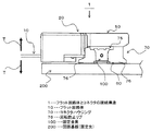
図1は、(a)が本発明の実施例に係るフラット回路体とコネクタの接続構造1の分解斜視図であり、(b)が(a)に示した端子80の拡大斜視図である。図2は、電極11と端子80を接続完了した状態のフラット回路体10およびコネクタ60の側面図である。図3は、(a)がコネクタハウジング70をフラット回路体10の挿入側とは逆側から視た図であり、(b)が(a)の端子圧入配置部73周辺を拡大した図である。図4は、図2(b)に対応した端子圧入配置部73に端子80を圧入固定した端子圧入配置部73周辺の拡大図である。図5は、コネクタ60を水平方向に切断した端子圧入配置部73周辺の断面図である。図6は、それぞれ異なる方向から視た端子80の図である。
本発明の実施例に係るフラット回路体とコネクタの接続構造1は、フラット回路体10の端末部10aをコネクタ60のコネクタハウジング70内にスライドしながら挿入することによって、端末部10aに形成した電極11と、コネクタハウジング70内に圧入固定した端子80と、を接続するものである。
なお、本発明の実施例では説明の便宜上、図中矢印に示すように上下および水平方向を定義し、水平方向が一対の突出圧入部93、93の突出方向に対応し、上下方向が一対の突出圧入部93、93の突出方向に直交する方向を示しているが、方向はこれに限定しない。例えば、水平方向が一対の突出圧入部93、93の突出方向に直交する方向としてもよい。
1A is an exploded perspective view of a connection structure 1 of a flat circuit body and a connector according to an embodiment of the present invention, and FIG. 1B is an enlarged perspective view of a
The flat circuit body-connector connection structure 1 according to the embodiment of the present invention includes an electrode formed on the
In the embodiment of the present invention, for convenience of explanation, the vertical and horizontal directions are defined as shown by arrows in the figure, the horizontal direction corresponds to the protruding direction of the pair of protruding press-
まず、フラット回路体10について説明する。
フラット回路体10は、例えば、フレキシブルプリント配線板によって実現する。このフラット回路体10は、絶縁性樹脂シートの上に導電性の金属膜によって回路配線を形成し、この回路配線を保護するように絶縁樹脂性シートの表面を絶縁保護フィルムによって覆った平板状可撓性の回路基板である。
また、フラット回路体10は、端末部10aの下面に回路配線として複数の電極11を並べて形成し、絶縁保護フィルムの一部を除去することによって各電極11の接続面を露出している。このようにして外部に露出した各電極11がコネクタ60に設けた各端子80に接続するようになっている。
また、フラット回路体10は、複数の電極11が露出される側とは反対側の面に補強板12を貼り付けている。この補強板12は、フラット回路体10の端末部10aに貼り付けることによって端末部10aを補強するものである。
さらに、フラット回路体10は、端末部10aにフラット回路体10を貫通する一対の係合孔13、13を形成している。この一対の係合孔13、13の各係合孔13は、スライドガイド部材20に設けた不図示の一対の係合突起のそれぞれに係合するようになっている。
First, the
The
The
Further, the
Further, the
次に、スライドガイド部材20について説明する。
スライドガイド部材20は、合成樹脂等の絶縁性樹脂材からなり、外郭が略直方体形状をなし、フラット回路体10の端末部10aに組み付ける部分となる回路体組付部30と、コネクタハウジング70のロック用突起77に係合してスライドガイド部材20をコネクタハウジング70に固定する部分となる接続ロック部40と、コネクタ60にスライドしながら挿入する際の取っ手部分となる操作用取手部50と、を有する。
Next, the
The
回路体組付部30は、フラット回路体10の一対の係合孔13、13に係合する不図示の一対の係合突起を形成し、フラット回路体10を一対の係合突起によって位置決めしつつ上下から挟持するように固定する回路体固定部31と、回路体固定部31のフラット回路体10に対して上側の面を挿入方向に向けて延在するように突出しフラット回路体10の端末部10aとともにコネクタハウジング70内に挿入する部分であるハウジング挿入部32と、を有する。
The
接続ロック部40は、支点に対してシーソーのように弾性的に可動する可動部41を有する。可動部41は、前端側にコネクタハウジング70のロック用突起77と係合するロックアーム部41aを設け、後端側にロックアーム部41aのロック用突起77との係合を解除するためのロック解除操作部41bを設けている。
The
このような接続ロック部40は、可動部41が弾性的に中立な状態では、ロックアーム部41aがロック用突起77と係合するように位置し、ロック解除操作部41bを下方に押圧操作することによって、ロックアーム部41aがロック用突起77との係合を解除できるようにその端部を上方に向けて傾けるようになっている。
Such a
次に、コネクタ60について説明する。
コネクタ60は、コネクタハウジング70と、コネクタハウジング70内に圧入固定した複数の端子80と、を有し、一対の固定金具100によって回路基板200等の固定先にコネクタハウジング70を固定するようになっている。
Next, the
The
コネクタハウジング70は、合成樹脂等の絶縁性樹脂材からなり、外郭が略直方体形状をなす。
このコネクタハウジング70は、複数の端子80を内部に圧入固定し、フラット回路体10の端末部10aを挿入する挿入口71からフラット回路体10をコネクタハウジング70内に挿入完了した位置で、スライドガイド部材20と上面に設けたロック用突起77を介して係合することによって各電極11と各端子80を接続した状態でフラット回路体10を固定するようになっている。
The
The
また、コネクタハウジング70は、挿入口71からコネクタハウジング70内に端末部10aを挿入するための挿入空間72を内部に形成し、挿入空間72に挿入した端末部10aの下方に複数の電極11に対応した並びで複数の端子80を圧入固定する端子圧入配置部73を設けている。
The
端子圧入配置部73は、端子80の圧入固定部90を圧入固定するため圧入固定部90を上下方向、および、水平方向で圧入固定部90を間にして向かい合う内壁面74を形成している。以下、水平方向で互いに向かい合う内壁面74を第一対向内壁面74a、74aと称する。また、第一対向内壁面74a、74に略直交する方向で向かい合う内壁面74を第二対向内壁面と称し、下側の第二対向内壁面に74bと符号を付し、上側の第二対向内壁面に74cと符号を付して区別できるようにしている。
The terminal press-
また、コネクタハウジング70の長手方向両側部には、各固定金具100を嵌め込んで固定する金具固定部75、75を設けている。この金具固定部75に固定した各固定金具100を回路基板200に固定することによって、コネクタハウジング70を固定先となる回路基板200に固定するようになっている。
Further, on both side portions of the
また、コネクタハウジング70の長手方向の各端部には、回路基板200に対してコネクタハウジング70が固定金具100を支点として回転することを防止する一対の回転防止リブ76、76をそれぞれ設けている。
この一対の回転防止リブ76、76は、固定金具100を間にして前方、および後方のそれぞれに突出するように設け、かつ、底面がコネクタハウジング70の底面の一部を構成するようになっている。
すなわち、一対の回転防止リブ76、76は、固定金具100を間にして互いに逆方向に突出し、かつ、コネクタハウジング70の底面の一部を構成することによって、固定金具100を間にして固定先となる回路基板200への接地面積を拡大している。このため、コネクタハウジング70が固定金具100を支点として回転しようとした場合、左右それぞれの回転方向に対して一対の回転防止リブのそれぞれの底面が回転を阻止するように回路基板200に当接するようになっている。
In addition, a pair of
The pair of
That is, the pair of
このような一対の回転防止リブ76、76は、図2中矢印Tに示すように、例えば、コネクタ60に接続しているフラット回路体10を上下方向に引っ張ることによって、固定金具100を支点として回転する力がコネクタハウジング70に作用した場合であっても、回転防止リブ76、76の底面がコネクタハウジング70の回転を防止し、結果的に、回路基板200に半田付けした端子80の半田が損傷することを防止している。
Such a pair of
なお、この実施例では、コネクタハウジング70の長手方向の各端部に前方、および、後方のそれぞれに突出するように一対の回転防止リブ76、76を設けるものを例示したが、これに限らず、固定金具100を間にして互いに逆方向に突出し、かつ、コネクタハウジング70の底面の一部を構成する少なくとも一対の回転防止リブ76、76を設けるようにすればよい。
In this embodiment, the
端子80は、ピン状の金属部材を曲げ加工等を施すことによって所定形状に形成したものであり、コネクタハウジング70内の端子圧入配置部73に圧入固定する圧入固定部90から電極11に向けて傾斜状に延びることで電極11に弾性的に接触する部分となる弾性接触片部80a、および、圧入固定部90を間にして弾性接触片部80aとは逆側にコネクタハウジング70の固定先となる回路基板に実装する部分となる実装部80bを含む。
The terminal 80 is formed in a predetermined shape by bending a pin-shaped metal member or the like, and is directed from the press-
弾性接触片部80aは、への字状に屈曲した屈曲部分周辺が電極11に接触するようになっている。この弾性接触片部80aは、フラット回路体10の端末部10aをコネクタハウジング70内にスライドしながら挿入すると、端末部10aから負荷される荷重によって下方に向けて弾性的にたわむため、弾性復元力によって電極11に接触した状態を保持できるようになっている。
The
圧入固定部90は、弾性接触片部80aと実装部80bとの間で圧入方向に沿って連続する部分となる固定本体部91と、固定本体部91の両側部から突出する一対の突出圧入部として、固定本体部91の延在方向で互いに離間した設けた一対の第一突出圧入部92、92、および、一対の第二突出圧入部93、93を有する。
The press-
一対の第一突出圧入部92、92は、固定本体部91の延在方向で弾性接触片部80a側の両側部から水平方向に突出し、端子圧入配置部73の互いに向かい合う水平対向内壁面74a、74aに接触することよって、圧入固定部90が端子圧入配置部73で圧入固定されるようになっている。
このため、圧入固定部90を端子圧入配置部73に圧入すると、一対の第一突出圧入部92、92が水平方向でのガタツキを抑えるようになっている。
The pair of first protruding press-
For this reason, when the press-fitting fixing
一対の第二突出圧入部93、93は、固定本体部91の延在方向で実装部80b側の両側部から水平方向に突出している。
この一対の第二突出圧入部93、93は、端子圧入配置部73に圧入固定した状態で、固定本体部91の両側部から端子圧入配置部73の各第一対向内壁面74a、74aに向けて水平方向に突出することによって第一対向内壁面74a、74aに接触し、かつ、第一対向内壁面74a、74aに略直交する方向で向かい合う端子圧入配置部73の一対の第二対向内壁面74b、74cの一方の第二対向内壁面74bから側部からの突出方向に向けて漸次離れる第一の面93a、および、他方の第二対向内壁面74cに側部からの突出方向に向けて漸次近づける第二の面93bを形成する。
The pair of second projecting press-
The pair of second protruding press-
なお、この実施例では、圧入固定部90は、一対の第二突出圧入部93、93を形成した部分の一対の第二突出圧入部93、93が突出する方向の断面が略U字形状になっている。このため、一対の第二突出圧入部93、93は、曲げ加工によって容易に成形することができるようになっている。
In this embodiment, the press-
このような圧入固定部90は、圧入固定部90が一対の第二突出圧入部93、93が互いに逆向きに側方に突出してそれぞれ第一対向内壁面74a、74aに接触しつつ、一対の第二突出圧入部93、93の間の部分が一対の第二対向内壁面74b、74cの一方の面74bに対峙する面を形成し、かつ、他方の面74cに対峙する面93bを突出方向に向けて他方の第二対向内壁面74cに漸次近づけることによって、一対の第二対向内壁面74b、74cが向かい合う方向で端子圧入配置部73との隙間が小さくなるようにし、しかも、一対の第二対向内壁面74b、74cのそれぞれに接触する面の面積を小さく抑えるようにしている。
これにより、圧入固定部90の一対の第二突出圧入部93、93を形成した部分では、コネクタハウジング70内で互いに直交する方向でのガタツキを抑えることができるようになっている。
Such a press-
Thereby, in the part which formed a pair of 2nd protrusion press-
また、圧入固定部90は、一対の第二突出圧入部93、93の第一の面93aを突出方向に向けて端子圧入配置部73の下側内壁面74bから上方に向けて漸次離れるように形成し、一対の第二突出圧入部93、93の上面93bを突出方向に向けて端子圧入配置部73の上側内壁面74cに漸次近づけるように形成しているので、端子圧入配置部73の下側内壁面74bおよび上側内壁面74cのそれぞれに接触する面の面積を小さく抑えるようにしているため、端子圧入配置部に端子を圧入する際に端子が端子圧入配置部の内壁面に干渉し難くなっている。
Further, the press-
実装部80bは、弾性接触片部80aとは逆方向に固定本体部91からクランク状に屈曲して延び、固定本体部91に対して略平行に延びる線上に沿って形成した端部を回路基板200にはんだ付けによって実装するようになっている。
The mounting
次に、図7および図8を用いて、フラット回路体10の端末部10aをコネクタハウジング70内にスライドしながら挿入することによって、電極11に接続する端子80の動作について説明する。
図7は、フラット回路体10の端末部10aをコネクタハウジング70内にスライドしながら挿入する様子を示したものであり、フラット回路体10および端子80を仮想線で示し、端子圧入配置部73の内壁面74を実線で示した図である。図8は、(a)が図7を端子80の実装部80b側から視た斜視図であり、(b)が(a)の一対の第二突出圧入部93、93のうち、一方の第二突出圧入部93周辺を拡大した図であり、(c)が図7を端子圧入配置部73への圧入口側から視た図であり、(d)が(c)の一対の第二突出圧入部93、93のうち、一方の第二突出圧入部93周辺を拡大した図である。
Next, the operation of the terminal 80 connected to the
FIG. 7 shows a state in which the
フラット回路体10の端末部10aをコネクタハウジング70内にスライドしながら挿入すると、端末部10aが端子80の弾性接触片部80aに上方から接触することによって、弾性接触片部80aが弾性的に下方にたわむように端子80に荷重が作用する。
When the
これにより、圧入固定部90を支点として実装部80bが上方に傾くように荷重が作用するものの、一対の第二突出圧入部93、93が突出方向に向けて端子圧入配置部73の上側内壁面74cに漸次近づける上面93bを形成し、圧入固定部90が、端子圧入配置部73の上下の内壁面74b、74cに対してもできるだけ近づくようになっているので、端子圧入配置部73での圧入固定部90の上下方向のガタツキが抑えられる。
Thereby, although a load acts so that the mounting
本発明の実施例に係るフラット回路体とコネクタの接続構造1は、圧入固定部90が一対の第二突出圧入部93、93が互いに逆向きに側方に突出してそれぞれ第一対向内壁面74a、74aに接触しつつ、一対の第二突出圧入部93、93の間の部分が一対の第二対向内壁面74b、74cの一方の面74bに対峙する面を形成し、かつ、他方の面74cに対峙する面93bを突出方向に向けて他方の第二対向内壁面74cに漸次近づけることによって、一対の第二対向内壁面74b、74cが向かい合う方向で端子圧入配置部73との隙間が小さくなるようにし、しかも、一対の第二対向内壁面74b、74cのそれぞれに接触する面の面積を小さく抑えるようにしているため、端子圧入配置部73に端子80を圧入する際に端子80が端子圧入配置部73の内壁面74に干渉し難くなっているので、コネクタハウジング70内で互いに直交する方向での端子80のガタツキを小さく抑えることによって端子80と端子80の実装先との接続定性を向上することができ、しかも、端子80をコネクタハウジング70内に圧入し難くなることを防ぐことができる。
In the flat circuit body and connector connection structure 1 according to the embodiment of the present invention, the press-
また、本発明の実施例に係るフラット回路体とコネクタの接続構造1は、圧入固定部90の一対の突出圧入部としての一対の第二突出圧入部93、93を形成した部分を曲げ加工によって容易に成形することができる。
In the flat circuit body and connector connection structure 1 according to the embodiment of the present invention, the portion where the pair of second projecting press-
また、本発明の実施例に係るフラット回路体とコネクタの接続構造1は、一対の回転防止リブ76、76が、固定金具100を間にして互いに逆方向に突出し、かつ、コネクタハウジング70の底面の一部を構成することによって、固定金具100を間にしてコネクタハウジング70の固定先への接地面積を拡大しているため、コネクタハウジング70が固定金具100を支点として回転しようとした場合、左右それぞれの回転方向に対して一対の回転防止リブ76、76のそれぞれの底面が回転を阻止するように固定先に当接するようになっているので、端子80が固定先に半田付けされている場合であっても、コネクタハウジング70の回転による端子80への負荷によって半田が損傷することを防ぐことができ、結果的に、端子80と固定先との電気的接続の低下を防止することができる。
Further, in the flat circuit body and connector connection structure 1 according to the embodiment of the present invention, the pair of
なお、本発明の実施例に係るフラット回路体とコネクタの接続構造1は、圧入固定部90、94が固定本体部90の両側部から突出する一対の突出圧入部として、一対の第一突出圧入部92、92と、一対の第二突出圧入部93、93と、を有するものを例示したが、これに限らず、一対の突出圧入部として少なくとも一対の第二突出圧入部93、93を有していればよい。
(変形例)
The flat circuit body and connector connection structure 1 according to the embodiment of the present invention includes a pair of first projecting press-fit portions as a pair of projecting press-fit portions in which the press-
(Modification)
次に、図9を用いて本発明の実施例に係るフラット回路体とコネクタの接続構造1の端子の変形例について説明する。
図9は、変形例の端子81をそれぞれ異なる方向から視た図である。
この変形例の端子81は、一対の第二突出圧入部95、95の形状が実施例の端子と異なる。
なお、その他の構成は実施例の端子と同様であり、実施例と同一構成部分には同一符号を付している。
Next, the modification of the terminal of the connection structure 1 of the flat circuit body and connector which concerns on the Example of this invention is demonstrated using FIG.
FIG. 9 is a diagram in which the terminal 81 according to the modification is viewed from different directions.
The terminal 81 of this modification differs from the terminal of an Example in the shape of a pair of 2nd protrusion press-
Other configurations are the same as those of the terminal of the embodiment, and the same components as those of the embodiment are denoted by the same reference numerals.
この変形例の端子81は、一対の第二突出圧入部95、95が固定本体部91の延在方向で実装部80b側の両側部から水平方向に突出している。
この一対の第二突出圧入部95、95は、端子圧入配置部73に圧入固定した状態で、固定本体部91の両側部から端子圧入配置部73の各第一対向内壁面74a、74aに向けて水平方向に突出することによって第一対向内壁面74a、74aに接触し、かつ、第一対向内壁面74a、74aに略直交する方向で向かい合う端子圧入配置部73の一対の第二対向内壁面74b、74cの一方の第二対向内壁面74bから側部からの突出方向に向けて漸次離れる第一の面95a、および、他方の第二対向内壁面74cに側部からの突出方向に向けて漸次近づける第二の面95bを形成する。
なお、一対の第二突出圧入部95、95の第一の面95a、および、第二の面95bが傾斜面になっている。
In the
The pair of second protruding press-
In addition, the
以上、本発明者によってなされた発明を、上述した発明の実施例に基づき具体的に説明したが、本発明は、上述した発明の実施例に限定されるものではなく、その要旨を逸脱しない範囲において種々変更可能である。 The invention made by the present inventor has been specifically described based on the above-described embodiments of the invention. However, the present invention is not limited to the above-described embodiments of the invention and does not depart from the gist thereof. Various changes can be made.
1 フラット回路体とコネクタの接続構造
10 フラット回路体
10a 端末部
11 電極
12 補強板
13 係合孔
20 スライドガイド部材
30 回路体組付部
31 回路体固定部
32 ハウジング挿入部
40 接続ロック部
41 可動部
41a ロック用アーム部
41b ロック解除操作部
50 操作用取手部
60 コネクタ
70 コネクタハウジング
71 挿入口
72 挿入空間
73 端子圧入配置部
74 内壁面
74a 第一対向内壁面(内壁面)
74b、74c 第二対向内壁面(内壁面)
75 金具固定部
76 回転防止リブ
77 ロック用突起
80、81 端子
80a 弾性接触片部
80b 実装部
90、94 圧入固定部
91 固定本体部
92 第一突出圧入部
93、95 第二突出圧入部(突出圧入部)
93a、95a 第一の面
93b、95b 第二の面
100 固定金具
200 回路基板
DESCRIPTION OF SYMBOLS 1 Connection structure of flat circuit body and
74b, 74c Second opposing inner wall surface (inner wall surface)
75 Metal fitting fixing
93a,
Claims (3)
前記圧入固定部は、
前記端子圧入配置部に圧入固定した状態で、前記弾性接触片部と前記実装部との間で圧入方向に沿って連続する部分の側方で向かい合う前記端子圧入配置部の一対の第一対向内壁面の各第一対向内壁面に向けて両側部から突出することによって前記一対の第一対向内壁面に接触し、かつ、前記第一対向内壁面に略直交する方向で向かい合う前記端子圧入配置部の一対の第二対向内壁面の一方の第二対向内壁面から前記側部からの突出方向に向けて漸次離れる第一の面、および、他方の前記第二対向内壁面に前記側部からの突出方向に向けて漸次近づける第二の面を形成する一対の突出圧入部
を有することを特徴とするフラット回路体とコネクタの接続構造。 By inserting the terminal part of the flat circuit body into the connector housing of the connector while sliding, the electrode formed on the terminal part and the press-fitting fixing part for press-fitting and fixing the terminal press-fitting arrangement part in the connector housing to the electrode An elastic contact piece part that elastically contacts the electrode by extending in a slanting direction, and a press-fit fixing part in the opposite side of the elastic contact piece part to the fixing destination of the connector housing In the connection structure of the flat circuit body and the connector for connecting the terminal including the mounting part to be the mounting part,
The press-fit fixing part is
In a state where the terminal press-fitting arrangement part is pressed and fixed, the pair of first opposing ends of the terminal press-fitting arrangement part facing the side of the continuous part along the press-fitting direction between the elastic contact piece part and the mounting part The terminal press-fitting arrangement portion that contacts the pair of first opposing inner wall surfaces by projecting from both sides toward each first opposing inner wall surface of the wall surface and faces in a direction substantially orthogonal to the first opposing inner wall surface A first surface of the pair of second opposing inner wall surfaces that gradually moves away from one second opposing inner wall surface in a protruding direction from the side portion, and the other second opposing inner wall surface from the side portion. A connection structure between a flat circuit body and a connector, comprising a pair of projecting press-fit portions that form a second surface that gradually approaches the projecting direction.
前記一対の突出圧入部を形成した部分の断面が略U字形状である
ことを特徴とする請求項1に記載のフラット回路体とコネクタの接続構造。 The press-fit fixing part is
The connection structure of the flat circuit body and the connector according to claim 1, wherein a cross section of a portion where the pair of protruding press-fitting portions is formed is substantially U-shaped.
固定先に固定金具によって固定し、前記固定金具を間にして互いに逆方向に突出し、かつ、該コネクタハウジングの底面の一部を構成する少なくとも一対の回転防止リブを有する
ことを特徴とする請求項1または2に記載のフラット回路体とコネクタの接続構造。 The connector housing is
A fixing bracket is fixed to a fixing destination, and has at least a pair of anti-rotation ribs protruding in opposite directions with the fixing bracket in between, and constituting a part of the bottom surface of the connector housing. A connection structure between the flat circuit body according to 1 or 2 and a connector.
Priority Applications (3)
| Application Number | Priority Date | Filing Date | Title |
|---|---|---|---|
| JP2015119606A JP2017004859A (en) | 2015-06-12 | 2015-06-12 | Connection structure for flat circuit body and connector |
| US15/176,879 US9595780B2 (en) | 2015-06-12 | 2016-06-08 | Connector, and connection mechanism of flat circuit body and connector |
| CN201610407332.0A CN106252929A (en) | 2015-06-12 | 2016-06-12 | The connecting structure of adapter and ffc body and adapter |
Applications Claiming Priority (1)
| Application Number | Priority Date | Filing Date | Title |
|---|---|---|---|
| JP2015119606A JP2017004859A (en) | 2015-06-12 | 2015-06-12 | Connection structure for flat circuit body and connector |
Publications (1)
| Publication Number | Publication Date |
|---|---|
| JP2017004859A true JP2017004859A (en) | 2017-01-05 |
Family
ID=57517303
Family Applications (1)
| Application Number | Title | Priority Date | Filing Date |
|---|---|---|---|
| JP2015119606A Abandoned JP2017004859A (en) | 2015-06-12 | 2015-06-12 | Connection structure for flat circuit body and connector |
Country Status (3)
| Country | Link |
|---|---|
| US (1) | US9595780B2 (en) |
| JP (1) | JP2017004859A (en) |
| CN (1) | CN106252929A (en) |
Families Citing this family (1)
| Publication number | Priority date | Publication date | Assignee | Title |
|---|---|---|---|---|
| JP7216685B2 (en) * | 2020-07-27 | 2023-02-01 | 矢崎総業株式会社 | connector |
Citations (5)
| Publication number | Priority date | Publication date | Assignee | Title |
|---|---|---|---|---|
| JPS4993379U (en) * | 1972-12-05 | 1974-08-13 | ||
| US5403209A (en) * | 1993-08-09 | 1995-04-04 | Burndy Corporation | Electrical connector having uniform contact receiving slots |
| JPH07220793A (en) * | 1994-01-31 | 1995-08-18 | Mitsumi Electric Co Ltd | Electric connector |
| JP2007005225A (en) * | 2005-06-27 | 2007-01-11 | Yazaki Corp | Connector fixing structure |
| JP2011134582A (en) * | 2009-12-24 | 2011-07-07 | Fujitsu Component Ltd | Connector for flat cable, method of manufacturing the same and lock mechanism |
Family Cites Families (5)
| Publication number | Priority date | Publication date | Assignee | Title |
|---|---|---|---|---|
| JPH0644039Y2 (en) * | 1989-08-04 | 1994-11-14 | 富士通株式会社 | connector |
| JP4259405B2 (en) * | 2004-06-15 | 2009-04-30 | 住友電装株式会社 | Board connector |
| JP5057592B2 (en) * | 2010-02-03 | 2012-10-24 | ヒロセ電機株式会社 | Circuit board electrical connector |
| JP5707138B2 (en) * | 2011-01-11 | 2015-04-22 | 矢崎総業株式会社 | connector |
| JP5973711B2 (en) * | 2011-11-25 | 2016-08-23 | ヒロセ電機株式会社 | Electrical connector |
-
2015
- 2015-06-12 JP JP2015119606A patent/JP2017004859A/en not_active Abandoned
-
2016
- 2016-06-08 US US15/176,879 patent/US9595780B2/en not_active Expired - Fee Related
- 2016-06-12 CN CN201610407332.0A patent/CN106252929A/en active Pending
Patent Citations (5)
| Publication number | Priority date | Publication date | Assignee | Title |
|---|---|---|---|---|
| JPS4993379U (en) * | 1972-12-05 | 1974-08-13 | ||
| US5403209A (en) * | 1993-08-09 | 1995-04-04 | Burndy Corporation | Electrical connector having uniform contact receiving slots |
| JPH07220793A (en) * | 1994-01-31 | 1995-08-18 | Mitsumi Electric Co Ltd | Electric connector |
| JP2007005225A (en) * | 2005-06-27 | 2007-01-11 | Yazaki Corp | Connector fixing structure |
| JP2011134582A (en) * | 2009-12-24 | 2011-07-07 | Fujitsu Component Ltd | Connector for flat cable, method of manufacturing the same and lock mechanism |
Also Published As
| Publication number | Publication date |
|---|---|
| US9595780B2 (en) | 2017-03-14 |
| CN106252929A (en) | 2016-12-21 |
| US20160365659A1 (en) | 2016-12-15 |
Similar Documents
| Publication | Publication Date | Title |
|---|---|---|
| JP5059571B2 (en) | Female terminal bracket for PCB | |
| US9190750B2 (en) | Board-to-board connector | |
| JP4494441B2 (en) | Electrical connector | |
| US8454397B2 (en) | Anti-wicking terminal and connector | |
| JP4970981B2 (en) | Electrical connector | |
| JP5809203B2 (en) | Flat conductor electrical connector | |
| JP5653202B2 (en) | connector | |
| JP2017204325A (en) | Connector for substrate | |
| JP2010129540A (en) | Electrical connector | |
| JP6006356B2 (en) | Contact and connector using the contact | |
| JP2007128876A (en) | Electric connector | |
| EP1686663A1 (en) | Electric connector having a receiving portion for receiving plying force when the connector is coupled to a mating connector | |
| JPWO2018012243A1 (en) | connector | |
| US7458848B2 (en) | Connector | |
| JP4482568B2 (en) | Electrical connector | |
| JP2000182694A (en) | Connector for circuit board connection | |
| WO2020050028A1 (en) | Connector | |
| JP2017004859A (en) | Connection structure for flat circuit body and connector | |
| JP2012221841A (en) | Electric connector for circuit board | |
| JP7420009B2 (en) | connector | |
| KR101463655B1 (en) | Electric connector | |
| JP4498890B2 (en) | Pair of header contacts and header connector using the same | |
| JP5993755B2 (en) | Electrical connector | |
| JP5271314B2 (en) | Surface mount connection terminals | |
| JP7433195B2 (en) | Connectors, connector modules, and electronic equipment |
Legal Events
| Date | Code | Title | Description |
|---|---|---|---|
| A131 | Notification of reasons for refusal |
Free format text: JAPANESE INTERMEDIATE CODE: A131 Effective date: 20170411 |
|
| A977 | Report on retrieval |
Free format text: JAPANESE INTERMEDIATE CODE: A971007 Effective date: 20170413 |
|
| A762 | Written abandonment of application |
Free format text: JAPANESE INTERMEDIATE CODE: A762 Effective date: 20170530 |