JP2016535487A - Latch comparator circuit and method - Google Patents
Latch comparator circuit and method Download PDFInfo
- Publication number
- JP2016535487A JP2016535487A JP2016525853A JP2016525853A JP2016535487A JP 2016535487 A JP2016535487 A JP 2016535487A JP 2016525853 A JP2016525853 A JP 2016525853A JP 2016525853 A JP2016525853 A JP 2016525853A JP 2016535487 A JP2016535487 A JP 2016535487A
- Authority
- JP
- Japan
- Prior art keywords
- terminal
- transistor
- coupled
- control terminal
- inverter
- Prior art date
- Legal status (The legal status is an assumption and is not a legal conclusion. Google has not performed a legal analysis and makes no representation as to the accuracy of the status listed.)
- Pending
Links
Images

Classifications
-
- H—ELECTRICITY
- H03—ELECTRONIC CIRCUITRY
- H03K—PULSE TECHNIQUE
- H03K3/00—Circuits for generating electric pulses; Monostable, bistable or multistable circuits
- H03K3/02—Generators characterised by the type of circuit or by the means used for producing pulses
- H03K3/353—Generators characterised by the type of circuit or by the means used for producing pulses by the use, as active elements, of field-effect transistors with internal or external positive feedback
- H03K3/356—Bistable circuits
- H03K3/356017—Bistable circuits using additional transistors in the input circuit
- H03K3/356034—Bistable circuits using additional transistors in the input circuit the input circuit having a differential configuration
-
- H—ELECTRICITY
- H03—ELECTRONIC CIRCUITRY
- H03K—PULSE TECHNIQUE
- H03K3/00—Circuits for generating electric pulses; Monostable, bistable or multistable circuits
- H03K3/02—Generators characterised by the type of circuit or by the means used for producing pulses
- H03K3/027—Generators characterised by the type of circuit or by the means used for producing pulses by the use of logic circuits, with internal or external positive feedback
- H03K3/037—Bistable circuits
- H03K3/0375—Bistable circuits provided with means for increasing reliability; for protection; for ensuring a predetermined initial state when the supply voltage has been applied; for storing the actual state when the supply voltage fails
-
- H—ELECTRICITY
- H03—ELECTRONIC CIRCUITRY
- H03K—PULSE TECHNIQUE
- H03K3/00—Circuits for generating electric pulses; Monostable, bistable or multistable circuits
- H03K3/02—Generators characterised by the type of circuit or by the means used for producing pulses
- H03K3/353—Generators characterised by the type of circuit or by the means used for producing pulses by the use, as active elements, of field-effect transistors with internal or external positive feedback
- H03K3/356—Bistable circuits
- H03K3/356069—Bistable circuits using additional transistors in the feedback circuit
Abstract
本開示は、信号をラッチするための回路および方法を含む。一実施形態では、2つのインバータが、信号をラッチするために背中合わせに構成される。各インバータは、インバータトランジスタの制御端子間に構成されるコンデンサを含む。一実施形態では、回路は、コンパレータの部分である。第1および第2の電圧が、差動トランジスタの制御端子上で受け取られ、差動出力信号が、2つの背中合わせのインバータに結合される。一実施形態では、回路がディセーブルにされ、インバータ中のトランジスタの制御端子上の電圧が、電源などの基準未満に設定され、回路の速度を増加する。The present disclosure includes circuits and methods for latching signals. In one embodiment, the two inverters are configured back to back to latch the signal. Each inverter includes a capacitor configured between the control terminals of the inverter transistors. In one embodiment, the circuit is part of a comparator. First and second voltages are received on the control terminals of the differential transistor, and the differential output signal is coupled to two back-to-back inverters. In one embodiment, the circuit is disabled and the voltage on the control terminal of the transistor in the inverter is set below a reference such as a power supply to increase the speed of the circuit.
Description
関連出願の相互参照
本出願は、すべての目的のために、その内容が全部参照により本明細書に組み込まれる、2013年10月29日に出願された、米国非仮特許出願第14/065,854号の優先権を主張する。
CROSS REFERENCE TO RELATED APPLICATIONS This application is a U.S. non-provisional patent application No. 14 / 065,854, filed Oct. 29, 2013, the contents of which are hereby incorporated by reference in their entirety for all purposes. Claim priority.
本開示は、電子システムおよび方法に関し、詳細には、ラッチ回路および方法に関する。 The present disclosure relates to electronic systems and methods, and in particular, to latch circuits and methods.
ラッチは、典型的には2つの安定な状態を有し、情報を取り込み、記憶するために使用できる回路である。情報をラッチすることは、様々なやり方で実装することができる。一例のラッチ回路は、デジタル信号を受け取るロジック回路であり、双安定な出力を有するように構成される。ここで、出力は、2つの安定状態のうちの1つへと解決する。ラッチとして一般に使用される例示的なロジック回路としては、インバータ、SRラッチ、JKラッチ、およびDラッチが挙げられる(「フリップフロップ」と呼ばれることがある)。 A latch is a circuit that typically has two stable states and can be used to capture and store information. Latching information can be implemented in various ways. An example latch circuit is a logic circuit that receives a digital signal and is configured to have a bistable output. Here, the output resolves to one of two stable states. Exemplary logic circuits commonly used as latches include inverters, SR latches, JK latches, and D latches (sometimes referred to as “flip-flops”).
コンパレータ回路は、比較動作の結果を取り込むためにラッチ回路を使用することがある。コンパレータの性能は、比較回路に続くラッチ回路の性能に大いに依存することになる場合がある。例えば、高速アナログデジタル変換器(「ADC」)(例えば、SAR、フラッシュADC)では、ADCの全変換時間は、コンパレータの速度に依存する場合があり、これは、最終出力に解決するためのラッチの能力に依存する。次に、ラッチの待ち時間は、電源電圧変動に依存する場合がある。例えば低い電源電圧において、相補型ラッチの待ち時間は、例えば低い電源電圧におけるバイアス電流の減少に起因して増加する。ラッチは、さらに、動作期間中の電源電圧の変動に対して安定でなければならない。したがって、電源電圧が減少するときに、電源電圧の変動に対して良好に機能するラッチ機能を実施するための、より速い回路を見いだす必要がある。 The comparator circuit may use a latch circuit to capture the result of the comparison operation. The performance of the comparator may depend greatly on the performance of the latch circuit following the comparison circuit. For example, in a high-speed analog-to-digital converter (“ADC”) (eg, SAR, flash ADC), the total conversion time of the ADC may depend on the speed of the comparator, which is a latch to resolve to the final output. Depends on ability. Next, the latch latency may depend on power supply voltage fluctuations. For example, at low power supply voltages, the complementary latch latency increases due to, for example, a decrease in bias current at low power supply voltages. The latch must also be stable against power supply voltage variations during operation. Therefore, there is a need to find a faster circuit for implementing a latch function that works well for power supply voltage fluctuations as the power supply voltage decreases.
本開示は、ラッチ回路および方法を含む。一実施形態では、本開示は、制御端子、第1の端子、および第2の端子を有する第1のトランジスタと、制御端子、第1の端子、および第2の端子を有する第2のトランジスタであって、第1のトランジスタの第1の端子が第2のトランジスタの第1の端子に結合される第2のトランジスタと、第1のインバータおよび第2のインバータであって、第1のインバータの出力が第2のインバータの入力に結合され、第2のインバータの出力が第1のインバータの入力に結合され、第1のインバータのバイアス端子が第1のトランジスタの第2の端子に結合され、第2のインバータのバイアス端子が第2のトランジスタの第2の端子に結合される第1のインバータおよび第2のインバータとを備える回路を含む。第1のインバータは、制御端子、第1の端子、および第2の端子を有する第3のトランジスタと、制御端子、第1の端子、および第2の端子を有する第4のトランジスタと、第3のトランジスタの制御端子と第4のトランジスタの制御端子との間に結合される第1のコンデンサとを備える。第2のインバータは、制御端子、第1の端子、および第2の端子を有する第5のトランジスタと、制御端子、第1の端子、および第2の端子を有する第6のトランジスタと、第5のトランジスタの制御端子と第6のトランジスタの制御端子との間に結合される第2のコンデンサとを備える。 The present disclosure includes latch circuits and methods. In one embodiment, the present disclosure includes a first transistor having a control terminal, a first terminal, and a second terminal, and a second transistor having a control terminal, the first terminal, and the second terminal. A first transistor having a first terminal coupled to a first terminal of the second transistor, a first inverter and a second inverter, wherein The output is coupled to the input of the second inverter, the output of the second inverter is coupled to the input of the first inverter, the bias terminal of the first inverter is coupled to the second terminal of the first transistor, A circuit comprising a first inverter and a second inverter, wherein the bias terminal of the second inverter is coupled to the second terminal of the second transistor. The first inverter includes a third transistor having a control terminal, a first terminal, and a second terminal, a fourth transistor having a control terminal, a first terminal, and a second terminal, and a third transistor And a first capacitor coupled between the control terminal of the first transistor and the control terminal of the fourth transistor. The second inverter includes a control terminal, a first terminal, and a fifth transistor having a second terminal, a control terminal, a first terminal, and a sixth transistor having a second terminal, And a second capacitor coupled between the control terminal of the first transistor and the control terminal of the sixth transistor.
一実施形態では、第1および第2のインバータがディセーブルであるとき、第3のトランジスタの制御端子上の電圧が、第4のトランジスタの制御端子上の電圧よりも低く、第5のトランジスタの制御端子上の電圧が、第6のトランジスタの制御端子上の電圧よりも低い。 In one embodiment, when the first and second inverters are disabled, the voltage on the control terminal of the third transistor is lower than the voltage on the control terminal of the fourth transistor, The voltage on the control terminal is lower than the voltage on the control terminal of the sixth transistor.
一実施形態では、第1および第2のインバータがディセーブルであるとき、第3、第4、第5、および第6のトランジスタの第1および第2の端子ならびに第4および第6のトランジスタの制御端子が基準電圧に結合され、第3および第5のトランジスタの制御端子が基準電圧未満の電圧に結合される。 In one embodiment, when the first and second inverters are disabled, the first and second terminals of the third, fourth, fifth, and sixth transistors and the fourth and sixth transistors The control terminal is coupled to a reference voltage, and the control terminals of the third and fifth transistors are coupled to a voltage less than the reference voltage.
一実施形態では、第1および第2のインバータがディセーブルであるとき、第3および第5のトランジスタの制御端子が、電源電圧未満の、MOSトランジスタ閾値電圧に結合される。 In one embodiment, when the first and second inverters are disabled, the control terminals of the third and fifth transistors are coupled to a MOS transistor threshold voltage that is less than the power supply voltage.
一実施形態では、回路は、第3のトランジスタの制御端子および第5のトランジスタの制御端子に結合される事前充電回路をさらに備える。 In one embodiment, the circuit further comprises a precharge circuit coupled to the control terminal of the third transistor and the control terminal of the fifth transistor.
一実施形態では、事前充電回路は、第3のトランジスタの制御端子に結合される第1の端子、および第2の端子を有する第7のトランジスタ、ならびに第5のトランジスタの制御端子に結合される第1の端子を有する第8のトランジスタを備える。 In one embodiment, the precharge circuit is coupled to the first terminal coupled to the control terminal of the third transistor, the seventh transistor having the second terminal, and the control terminal of the fifth transistor. An eighth transistor having a first terminal is provided.
一実施形態では、第7のトランジスタの第2の端子および第8のトランジスタの第2の端子が基準発生器に結合される。 In one embodiment, the second terminal of the seventh transistor and the second terminal of the eighth transistor are coupled to the reference generator.
一実施形態では、基準発生器は、第7のトランジスタの第2の端子および第8のトランジスタの第2の端子に結合される制御端子を有する第9のトランジスタを備え、第9のトランジスタが、基準電圧に結合される第1の端子ならびに第9のトランジスタの制御端子および負荷に結合される第2の端子をさらに備える。 In one embodiment, the reference generator comprises a ninth transistor having a control terminal coupled to the second terminal of the seventh transistor and the second terminal of the eighth transistor, wherein the ninth transistor comprises: A first terminal coupled to the reference voltage and a control terminal of the ninth transistor and a second terminal coupled to the load are further included.
一実施形態では、事前充電回路が、第3のトランジスタの制御端子に結合される第1の端子および基準発生器に結合される第2の端子を有する第1の抵抗器、ならびに第5のトランジスタの制御端子に結合される第1の端子および基準発生器に結合される第2の端子を有する第2の抵抗器を備える。 In one embodiment, the precharge circuit includes a first resistor having a first terminal coupled to the control terminal of the third transistor and a second terminal coupled to the reference generator, and a fifth transistor. A second resistor having a first terminal coupled to the control terminal and a second terminal coupled to the reference generator.
一実施形態では、基準発生器が、第1の抵抗器の第2の端子および第2の抵抗器の第2の端子に結合される制御端子を有する第9のトランジスタを備え、第9のトランジスタが、基準電圧に結合される第1の端子ならびに第9のトランジスタの制御端子および負荷に結合される第2の端子をさらに備える。 In one embodiment, the reference generator comprises a ninth transistor having a control terminal coupled to the second terminal of the first resistor and the second terminal of the second resistor, the ninth transistor Further comprises a first terminal coupled to the reference voltage and a control terminal of the ninth transistor and a second terminal coupled to the load.
別の実施形態では、下に記載される技法が、方法を含む。一実施形態では、方法は、第1のトランジスタの制御端子上に第1の入力電圧を受け取るステップであって、第1のトランジスタが第1の端子および第2の端子を有するステップと、第2のトランジスタの制御端子上に第2の入力電圧を受け取るステップであって、第2のトランジスタが第1の端子および第2の端子を有し、第2のトランジスタの第1の端子が第1のトランジスタの第1の端子に結合され、第1の基準電圧に選択的に結合されるステップと、第1のトランジスタの第2の端子からの差動信号の第1の成分を第1のインバータのバイアス端子に結合するステップと、第2のトランジスタの第2の端子からの差動信号の第2の成分を第2のインバータのバイアス端子に結合するステップであって、第1のインバータの出力が第2のインバータの入力に結合され、第2のインバータの出力が第1のインバータの入力に結合されるステップと、第2のインバータの出力からの出力信号を、第1のインバータの入力において第4のトランジスタの制御端子および第1のコンデンサの第1の端子に結合して、出力信号を第1のコンデンサを通して第3のトランジスタの制御端子に結合するステップと、第1のインバータの出力からの出力信号を、第2のインバータの入力において第6のトランジスタの制御端子および第2のコンデンサの第1の端子に結合して、出力信号を第2のコンデンサを通して第5のトランジスタの制御端子に結合するステップとを含む。 In another embodiment, the technique described below includes a method. In one embodiment, the method receives a first input voltage on a control terminal of a first transistor, the first transistor having a first terminal and a second terminal, and a second Receiving a second input voltage on a control terminal of the second transistor, wherein the second transistor has a first terminal and a second terminal, and the first terminal of the second transistor is the first terminal A step coupled to the first terminal of the transistor and selectively coupled to the first reference voltage; and a first component of the differential signal from the second terminal of the first transistor is coupled to the first inverter. Coupling to the bias terminal and coupling the second component of the differential signal from the second terminal of the second transistor to the bias terminal of the second inverter, the output of the first inverter being Coupled to the input of the second inverter, the second A step in which the output of the inverter is coupled to the input of the first inverter, and the output signal from the output of the second inverter is connected to the control terminal of the fourth transistor and the Coupling the output signal to the control terminal of the third transistor through the first capacitor and coupling the output signal from the output of the first inverter to the sixth inverter at the input of the second inverter. Coupling the output signal to the control terminal of the fifth transistor through the second capacitor and coupling to the control terminal of the second transistor and the first terminal of the second capacitor.
一実施形態では、方法は、第3のトランジスタの制御端子および第5のトランジスタの制御端子を事前充電するステップをさらに含む。 In one embodiment, the method further comprises precharging the control terminal of the third transistor and the control terminal of the fifth transistor.
一実施形態では、事前充電するステップは、第3のトランジスタの制御端子に結合される第1の端子を有する第7のトランジスタ、および第5のトランジスタの制御端子に結合される第1の端子を有する第8のトランジスタを通して、第2の基準電圧を選択的に結合するステップを含む。 In one embodiment, the step of precharging includes a seventh transistor having a first terminal coupled to the control terminal of the third transistor, and a first terminal coupled to the control terminal of the fifth transistor. Selectively coupling the second reference voltage through the eighth transistor having.
一実施形態では、方法は、第3の基準電圧に結合される第1の端子ならびに第9のトランジスタの制御端子および負荷に結合される第2の端子を有する第9のトランジスタ中の第2の基準電圧を生成するステップをさらに含む。 In one embodiment, a method includes a second terminal in a ninth transistor having a first terminal coupled to a third reference voltage and a second terminal coupled to a control terminal of the ninth transistor and a load. The method further includes generating a reference voltage.
一実施形態では、事前充電するステップは、第3のトランジスタの制御端子に結合される第1の端子を有する第1の抵抗器、および第5のトランジスタの制御端子に結合される第1の端子を有する第2の抵抗器を通して、第2の基準電圧を結合するステップを含む。 In one embodiment, the precharging step comprises: a first resistor having a first terminal coupled to the control terminal of the third transistor; and a first terminal coupled to the control terminal of the fifth transistor. Coupling a second reference voltage through a second resistor having:
一実施形態では、方法は、第3の基準電圧に結合される第1の端子ならびに第9のトランジスタの制御端子および負荷に結合される第2の端子を有する第9のトランジスタ中の第2の基準電圧を生成するステップをさらに含む。 In one embodiment, a method includes a second terminal in a ninth transistor having a first terminal coupled to a third reference voltage and a second terminal coupled to a control terminal of the ninth transistor and a load. The method further includes generating a reference voltage.
一実施形態では、第1および第2のインバータがディセーブルであるとき、第3のトランジスタの制御端子上の電圧が、第4のトランジスタの制御端子上の電圧よりも低く、第5のトランジスタの制御端子上の電圧が、第6のトランジスタの制御端子上の電圧よりも低い。 In one embodiment, when the first and second inverters are disabled, the voltage on the control terminal of the third transistor is lower than the voltage on the control terminal of the fourth transistor, The voltage on the control terminal is lower than the voltage on the control terminal of the sixth transistor.
一実施形態では、第1および第2のインバータがディセーブルであるとき、第3、第4、第5、および第6のトランジスタの第1および第2の端子ならびに第4および第6のトランジスタの制御端子が基準電圧に結合され、第3および第5のトランジスタの制御端子が基準電圧未満の電圧に結合される。 In one embodiment, when the first and second inverters are disabled, the first and second terminals of the third, fourth, fifth, and sixth transistors and the fourth and sixth transistors The control terminal is coupled to a reference voltage, and the control terminals of the third and fifth transistors are coupled to a voltage less than the reference voltage.
一実施形態では、第1および第2のインバータがディセーブルであるとき、第3および第5のトランジスタの制御端子が、電源電圧未満の、MOSトランジスタ閾値電圧に結合される。 In one embodiment, when the first and second inverters are disabled, the control terminals of the third and fifth transistors are coupled to a MOS transistor threshold voltage that is less than the power supply voltage.
別の実施形態では、本開示は、第1の電圧および第2の電圧を受け取り、差動信号を作り出すための手段と、直列に構成される第1の対のトランジスタを備え、第1の対のトランジスタの制御端子間に構成される第1のコンデンサを有する第1のロジック回路であって、第1のインバータのバイアス端子が差動信号の第1の成分を受け取る第1のロジック回路と、直列に構成される第2の対のトランジスタを備え、第2の対のトランジスタの制御端子間に構成される第2のコンデンサを有する第2のロジック回路であって、第2のインバータのバイアス端子が差動信号の第2の成分を受け取る第2のロジック回路とを備え、第1のロジック回路の出力が第2のロジック回路の入力に結合され、第2のロジック回路の出力が第1のロジック回路の入力に結合されて双安定な出力を作り出す回路を含む。 In another embodiment, the present disclosure comprises a means for receiving a first voltage and a second voltage and producing a differential signal, and a first pair of transistors configured in series, the first pair A first logic circuit having a first capacitor configured between the control terminals of the transistors, wherein the bias terminal of the first inverter receives the first component of the differential signal; A second logic circuit comprising a second pair of transistors configured in series and having a second capacitor configured between the control terminals of the second pair of transistors, the bias terminal of the second inverter And a second logic circuit that receives a second component of the differential signal, the output of the first logic circuit is coupled to the input of the second logic circuit, and the output of the second logic circuit is the first logic circuit Coupled to the input of the logic circuit and bistable Including a circuit to create a force.
以下の詳細な記載および添付図面は、本開示の性質および利点のより良好な理解をもたらす。 The following detailed description and the accompanying drawings provide a better understanding of the nature and advantages of the present disclosure.
本開示は、ラッチ回路およびラッチコンパレータに関する。以下の記載では、説明の目的で、本開示の完全な理解を実現するため、多くの例および具体的な詳細が記載される。しかし、当業者には、請求項に表現されるような本開示は、これらの例の中のみ、または下に記載される他の特徴と組み合わせた特徴のいくつかまたはすべてを含むことができ、本明細書に記載される特徴および概念の修正形態および等価物をさらに含むことができることが明らかであろう。 The present disclosure relates to a latch circuit and a latch comparator. In the following description, for purposes of explanation, numerous examples and specific details are set forth in order to provide a thorough understanding of the present disclosure. However, for those skilled in the art, the present disclosure as expressed in the claims may include some or all of the features only in these examples or in combination with other features described below, It will be apparent that modifications and equivalents of the features and concepts described herein may be further included.
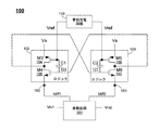
図1は、一実施形態に従う例示のラッチコンパレータ回路を図示する。ラッチコンパレータ回路100は、差動回路101ならびに双安定な出力を作り出すように構成される1対の交差結合されたロジック回路102および103を含む。差動回路101は、2つの電圧Vin1およびVin2を受け取り、成分Idiff1およびIdiff2を有する差動出力電流信号を作り出す。第1のロジック回路102は、電源電圧Vsに結合される第1のバイアス端子、およびIdiff1を受け取るため差動回路101の第1の出力端子に結合される第2のバイアス端子150を有する。同様に、第2のロジック回路103は、電源電圧Vsに結合される第1のバイアス端子、およびIdiff2を受け取るため差動回路101の第2の出力端子に結合される第2のバイアス端子151を有する。ロジック回路102の入力は、ロジック回路103の出力に結合され、ロジック回路103の入力は、ロジック回路102の出力に結合され、その結果、一方のロジック回路の出力がハイであるとき、他方がローである。
FIG. 1 illustrates an exemplary latch comparator circuit according to one embodiment.
Vin1とVin2の間の電圧差が、Idiff1とIdiff2の電流差をもたらす。例えば、Vin1がVin2よりも低いとき、端子150から差動回路101への電流は、端子151からの電流よりも小さい可能性があり、このことによって、ノード150における電圧が、ノード151における電圧よりも高くなる。同様に、Vin1がVin2よりも高いとき、端子150から差動回路101への電流は、端子151からの電流よりも大きい可能性があり、このことによって、ノード150における電圧が、ノード151における電圧よりも低い可能性がある。ノード150における電圧がノード151における電圧よりも低いとき、ロジック回路102の出力がローに引っ張られ、ロジック回路103の出力がハイに引っ張られる。ロジック回路は、ロジック回路102の出力がロー、およびロジック回路103の出力がハイで安定する。同様に、ノード150における電圧がノード151における電圧よりも高いとき、ロジック回路102の出力がハイに引っ張られ、ロジック回路103の出力がローに引っ張られる。ロジック回路は、ロジック回路102の出力がハイ、およびロジック回路103の出力がローで安定することになる。したがって、電圧Vin1およびVin2によって、ラッチコンパレータ回路100の出力に、2つの状態のうちの1つをとらせる(出力は双安定である)。
The voltage difference between Vin1 and Vin2 results in the current difference between Idiff1 and Idiff2. For example, when Vin1 is lower than Vin2, the current from
ラッチ機能を実装するため、様々なロジック回路を様々な実施形態で使用することができるが、本例は、直列に構成されるトランジスタ対を各々が備える2つのインバータを使用することを説明する。例えば、ロジック回路102は、電源電圧Vsと差動回路101の端子150との間に直列に構成される、PMOSトランジスタ104(M3)およびNMOSトランジスタ105(M4)を含む。同様に、ロジック回路103は、電源電圧Vsと差動回路101の別の端子151との間に直列に構成される、PMOSトランジスタ106(M5)およびNMOSトランジスタ107(M6)を含む。各トランジスタは、示されるように構成される、制御端子(例えば、ゲート)ならびに第1および第2の端子(例えば、ソースおよびドレイン)を含む。
Although various logic circuits can be used in various embodiments to implement the latching function, this example illustrates the use of two inverters, each with a pair of transistors configured in series. For example, the
本開示の特徴および利点は、各ロジック回路におけるトランジスタの制御端子間にコンデンサを構成することを含む。例えば、コンデンサ120(C1)が、トランジスタ104および105の制御端子間に構成される。同様に、コンデンサ121(C2)が、トランジスタ106および107の制御端子間に構成される。一実施形態では、回路は、相互コンダクタンスおよび回路の速度を増加させるために、特定の動作点の期間、トランジスタ104および106の制御端子上の電圧が、トランジスタ105および107の制御端子上の電圧よりも低い場合があるように構成される。したがって、1つの例示的な実施形態は、PMOS相補型デバイスのゲート電圧をずらすためにAC結合を使用するAC結合再生ラッチを含み、より低い電源電圧においてラッチの速度を増加させるために、より大きい電流が再生ラッチを通して流れることを可能にする。
Features and advantages of the present disclosure include configuring a capacitor between the control terminals of the transistors in each logic circuit. For example, a capacitor 120 (C1) is configured between the control terminals of the
一実施形態では、本開示に従う回路は、事前充電回路110を含むことができる。事前充電回路110は、トランジスタ104および106の制御端子に基準電圧Vrefを選択的に結合し、コンデンサC1およびC2上に電圧を設定して、トランジスタ104および106にバイアスを加えることができる。一実施形態では、ラッチコンパレータ回路100は、ディセーブル状態およびイネーブル状態で動作することができる。ディセーブル状態(または、セットアップ状態)の期間、回路の中のノードを特定の電圧に結合することができ、入力電圧Vin1およびVin2が受け取られる。回路は、次いでイネーブルにされ、その結果、回路が入力電圧に応答して、出力が、2つの安定な出力状態のうちの1つに解決することができる。ディセーブル状態の期間、事前充電回路は、Vrefをトランジスタ104および106の制御端子に提供してバイアスを設定し、回路がイネーブル状態に移行するときの回路の速度を改善することができる。例えば、回路がイネーブルであるとき、事前充電回路は高インピーダンスを呈し、VrefがコンデンサC1およびC2上に格納され、トランジスタ104および106上のバイアス点を設定し、回路の相互コンダクタンスを増加させる。
In one embodiment, a circuit according to the present disclosure may include a
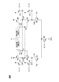
図2は、別の実施形態に従うラッチコンパレータ回路の例示的な実装を図示する。ラッチコンパレータ回路200は、差動的に構成されたトランジスタ201および202を含む。トランジスタ201は、制御端子上に第1の入力電圧Vipを受け取り、差動信号の第1の成分Idiff1を生成する。同様に、トランジスタ202は、制御端子上に第1の入力電圧Vinを受け取り、差動信号の第2の成分Idiff2を生成する。トランジスタ201および202の第2の端子は、互いに、かつトランジスタ203の端子に結合される。トランジスタ203は、制御端子上で「ラッチ」信号を受け取り、トランジスタ203の他の端子は、グランド(GND)などの基準電圧に結合されて、トランジスタ201および202のソースをグランドに選択的に結合する。例えば、ラッチ信号がハイであり、トランジスタ203がオンであるとき、Idiff1およびIdiff2は、トランジスタ201および202により生成される差動電流であってよい。
FIG. 2 illustrates an exemplary implementation of a latch comparator circuit according to another embodiment. The
差動電流Idiff1およびIdiff2は、トランジスタ204〜207およびコンデンサC1およびC2を備える、1対の交差結合されたインバータへと流れる。トランジスタ204〜205を備える一方のインバータの出力out1は、トランジスタ206〜207を備える他方のインバータの入力in2に結合される。同様に、トランジスタ204〜205を備えるインバータの入力in1は、トランジスタ206および207を備えるインバータの出力out2に結合される。差動電流Idiff1およびIdiff2は、トランジスタ205および207のソースに結合され、このことによって、ラッチがアクティブであるとき、交差結合されたインバータに、2つの状態のうちの1つをとらせる。したがって、トランジスタ204および205の両方のドレイン端子は、(VipおよびVinに依存して)ハイまたはローとなり、トランジスタ206および207のドレイン端子は、ローまたはハイになる(トランジスタ204および205のドレイン端子の逆)。
Differential currents Idiff1 and Idiff2 flow to a pair of cross-coupled inverters comprising transistors 204-207 and capacitors C1 and C2. The output out1 of one inverter comprising transistors 204-205 is coupled to the input in2 of the other inverter comprising transistors 206-207. Similarly, the input in1 of the inverter comprising transistors 204-205 is coupled to the output out2 of the
第1の時間期間(例えば、ディセーブル状態)の間、ラッチ信号はローであり、回路の中のノードは、スイッチS1〜S4によって基準電圧(Vs)に設定される。この時間期間の間、トランジスタ203はオフになり、トランジスタ201および202のソース端子はフローティングである。ラッチ信号がハイ(例えば、イネーブル状態)になると、トランジスタ203がオンになり、スイッチS1〜S4が開き、差動トランジスタ対が、VipとVinの間の差を解決して、2つの状態のうちの1つへと交差結合されたインバータを駆動する。
During the first time period (eg, disabled state), the latch signal is low and the nodes in the circuit are set to the reference voltage (Vs) by switches S1-S4. During this time period,
ラッチコンパレータ回路200は、事前充電回路220と221の対を含む。各事前充電回路は、基準電圧V1と、各インバータの差動出力トランジスタ204および206の制御端子との間に構成される。ラッチ信号がローであるとき、事前充電回路は、コンデンサC1およびC2上に電圧を設定して、出力トランジスタ204および206上にバイアスを設定する。例えば、ラッチ信号がローであるとき、事前充電回路は、トランジスタ204および206の制御端子上の電圧をV1に等しく設定することができる。ラッチ信号がハイになると、差動トランジスタ201および202からの信号をラッチするときに、各コンデンサC1およびC2が電圧V1を維持するように、事前充電回路が、トランジスタ204および206の制御端子をV1から分離することができる。トランジスタ204および206の制御端子上の電圧が、トランジスタ205および207の制御端子上の電圧よりも低いように、電圧V1を設定することができる。したがって、トランジスタ204および206は、例えばラッチコンパレータの速度を改善するために、より低い電源電圧において、より強くバイアスをかけられる。
ラッチが解決すると、第1のインバータ出力out1における信号は、第2のインバータの中の入力トランジスタ207の制御端子に結合され、コンデンサC2を通して出力トランジスタ206の制御端子にAC結合される。同様に、第2のインバータ出力out2における信号は、第1のインバータの中の入力トランジスタ205の制御端子に結合され、コンデンサC1を通して出力トランジスタ204の制御端子にAC結合される。トランジスタ204および206のゲートにコンデンサC1およびC2を通して提供される追加信号は、各インバータの相互コンダクタンスを以下のように改善する。
インバータ1の実効相互コンダクタンス:GInv1 = Gm3 + (C2/(C2+Cg5))Gm5
インバータ2の実効相互コンダクタンス:GInv2 = Gm4 + (C1/(C1+Cg6))Gm6
実効容量:Co1 = Cg3 + (C2/(C2+Cg5))Cg5 + CL1
実効容量:Co2 = Cg4 + (C1/(C1+Cg6))Cg6 + CL2
When the latch is resolved, the signal at the first inverter output out1 is coupled to the control terminal of the
Effective transconductance of inverter 1: G Inv1 = G m3 + (C 2 / (C 2 + C g5 )) G m5
Effective transconductance of inverter 2: G Inv2 = G m4 + (C 1 / (C 1 + C g6 )) G m6
Effective capacity: C o1 = C g3 + (C 2 / (C 2 + C g5 )) C g5 + C L1
Effective capacity: C o2 = C g4 + (C 1 / (C 1 + C g6 )) C g6 + C L2
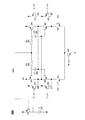
図3は、一実施形態に従う例示の事前充電回路を図示する。この例では、事前充電回路は、ダイオード構成のPMOSトランジスタ250から基準電圧を受け取るように構成される、PMOSトランジスタ240およびPMOSトランジスタ241を備える。トランジスタ250は、Vsなどの基準電圧に結合される第1の制御端子、ならびにゲート端子および負荷(例えば、電流源(I1))251に結合される第2の端子を有する。トランジスタ250のゲート端子は、電圧Vrefを生成し、これは、トランジスタ240および241の端子に結合される。したがって、ダイオード構成のPMOSトランジスタ250は、Vrefを生成し、これは、電源電圧Vs未満のMOSトランジスタ閾値電圧である。この例では、PMOSトランジスタ204および206にバイアスをかけるために、PMOSトランジスタ閾値電圧を使用することができる。
FIG. 3 illustrates an exemplary precharge circuit according to one embodiment. In this example, the precharge circuit comprises a
ディセーブル状態期間に、ラッチ信号がローであるとき、トランジスタ240および241がオンになり、電圧Vrefが、トランジスタ204および206のゲート端子に結合される。ゲート端子上にバイアス電圧を設定するため、VrefがコンデンサC1およびC2を充電する。ラッチコンパレータ回路300がイネーブルであるとき、ラッチ信号電圧がハイになってトランジスタ240および241がオフになり、このことによって、トランジスタ204および206のゲート端子をVrefから効果的に切り離す。同時に、この例では、スイッチS1〜S4が開となり、トランジスタ203がアクティブ化され、ラッチコンパレータ回路が、入力電圧VipおよびVinを解決し始める。コンデンサC1およびC2上に格納されるバイアス電圧に起因する、トランジスタ204および206の改善された相互コンダクタンスのために、入力電圧VipおよびVinは、出力により速く伝播する。
During the disabled state, when the latch signal is low,
図4は、別の実施形態に従う事前充電回路の別の例を図示する。この例では、ラッチコンパレータ回路400は、抵抗器(R1)260および抵抗器(R2)261を備える事前充電回路を含む。基準電圧Vrefは、抵抗器260および261を通して、PMOSトランジスタ204および206のゲート端子に結合され、PMOSトランジスタ204および206のゲート端子に、電源電圧Vs未満のPMOS閾値電圧でバイアスをかける。したがって、ディセーブル状態では、電圧VrefがコンデンサC1およびC2上に格納される。ラッチコンパレータ回路400がイネーブルであるとき、抵抗器260および261は、Vrefからの分離を実現し、その結果、入力電圧VipおよびVinに応答して、ラッチのインバータが安定な出力のうちの1つに解決するとき、トランジスタ204および206がそれらのバイアスを維持する。
FIG. 4 illustrates another example of a precharge circuit according to another embodiment. In this example, latch
上の記載は、本開示の様々な実施形態、ならびに特定の実施形態のどんな態様の例が実装され得るのかを説明する。上の例が唯一の実施形態であると考えるべきでなく、以下の請求項により規定されるような特定の実施形態のフレキシビリティおよび利点を説明するために提示される。上の記載および下の請求項に基づいて、請求項により規定されるような本開示の範囲から逸脱することなく、他の配置、実施形態、実装および等価物を採用することができる。 The above description illustrates various embodiments of the present disclosure, as well as what aspects of certain embodiments may be implemented. The above examples should not be considered to be the only embodiments, but are presented to illustrate the flexibility and advantages of certain embodiments as defined by the following claims. Based on the above description and the claims below, other arrangements, embodiments, implementations and equivalents can be employed without departing from the scope of the present disclosure as defined by the claims.
100 ラッチコンパレータ回路
101 差動回路
102 ロジック回路
103 ロジック回路
104 トランジスタ
105 トランジスタ
106 トランジスタ
107 トランジスタ
110 事前充電回路
120 コンデンサ
121 コンデンサ
150 バイアス端子、ノード
151 バイアス端子、ノード
200 ラッチコンパレータ回路
201 トランジスタ
202 トランジスタ
203 トランジスタ
204 トランジスタ
205 トランジスタ
206 トランジスタ
207 トランジスタ
220 事前充電回路
221 事前充電回路
240 トランジスタ
241 トランジスタ
250 トランジスタ
260 抵抗器(R1)
261 抵抗器(R2)
400 ラッチコンパレータ回路
100 Latch comparator circuit
101 Differential circuit
102 Logic circuit
103 logic circuit
104 transistor
105 transistors
106 transistors
107 transistors
110 Pre-charge circuit
120 capacitors
121 capacitors
150 Bias pin, node
151 Bias pin, node
200 Latch comparator circuit
201 transistors
202 transistors
203 transistor
204 transistors
205 transistors
206 transistors
207 transistor
220 Pre-charge circuit
221 Pre-charging circuit
240 transistors
241 transistor
250 transistors
260 Resistor (R1)
261 Resistor (R2)
400 Latch comparator circuit
Claims (20)
制御端子、第1の端子、および第2の端子を有する第1のトランジスタと、
制御端子、第1の端子、および第2の端子を有する第2のトランジスタであって、前記第1のトランジスタの前記第1の端子が前記第2のトランジスタの前記第1の端子に結合される、第2のトランジスタと、
第1のインバータおよび第2のインバータであって、前記第1のインバータの出力が前記第2のインバータの入力に結合され、前記第2のインバータの出力が前記第1のインバータの入力に結合され、前記第1のインバータのバイアス端子が前記第1のトランジスタの前記第2の端子に結合され、前記第2のインバータのバイアス端子が前記第2のトランジスタの前記第2の端子に結合される、第1のインバータおよび第2のインバータと
を備え、
前記第1のインバータが、
制御端子、第1の端子、および第2の端子を有する第3のトランジスタ、
制御端子、第1の端子、および第2の端子を有する第4のトランジスタ、ならびに
前記第3のトランジスタの前記制御端子と前記第4のトランジスタの前記制御端子との間に結合される第1のコンデンサ
を備え、
前記第2のインバータが、
制御端子、第1の端子、および第2の端子を有する第5のトランジスタ、
制御端子、第1の端子、および第2の端子を有する第6のトランジスタ、ならびに
前記第5のトランジスタの前記制御端子と前記第6のトランジスタの前記制御端子との間に結合される第2のコンデンサ
を備える、回路。 A circuit,
A first transistor having a control terminal, a first terminal, and a second terminal;
A second transistor having a control terminal, a first terminal, and a second terminal, wherein the first terminal of the first transistor is coupled to the first terminal of the second transistor A second transistor,
A first inverter and a second inverter, wherein the output of the first inverter is coupled to the input of the second inverter, and the output of the second inverter is coupled to the input of the first inverter; The bias terminal of the first inverter is coupled to the second terminal of the first transistor, and the bias terminal of the second inverter is coupled to the second terminal of the second transistor; Comprising a first inverter and a second inverter;
The first inverter is
A third transistor having a control terminal, a first terminal, and a second terminal;
A fourth transistor having a control terminal, a first terminal, and a second terminal; and a first transistor coupled between the control terminal of the third transistor and the control terminal of the fourth transistor With a capacitor,
The second inverter is
A fifth transistor having a control terminal, a first terminal, and a second terminal;
A sixth transistor having a control terminal, a first terminal, and a second terminal; and a second transistor coupled between the control terminal of the fifth transistor and the control terminal of the sixth transistor A circuit with a capacitor.
第2のトランジスタの制御端子上に第2の入力電圧を受け取るステップであって、前記第2のトランジスタが第1の端子および第2の端子を有し、前記第2のトランジスタの前記第1の端子が前記第1のトランジスタの前記第1の端子に結合され、第1の基準電圧に選択的に結合される、ステップと、
前記第1のトランジスタの前記第2の端子からの差動信号の第1の成分を第1のインバータのバイアス端子に結合するステップと、
前記第2のトランジスタの前記第2の端子からの前記差動信号の第2の成分を第2のインバータのバイアス端子に結合するステップであって、前記第1のインバータの出力が前記第2のインバータの入力に結合され、前記第2のインバータの出力が前記第1のインバータの入力に結合される、ステップと、
前記第2のインバータの前記出力からの出力信号を、前記第1のインバータの前記入力において第4のトランジスタの制御端子および第1のコンデンサの第1の端子に結合して、前記出力信号を前記第1のコンデンサを通して第3のトランジスタの制御端子に結合するステップと、
前記第1のインバータの前記出力からの出力信号を、前記第2のインバータの前記入力において第6のトランジスタの制御端子および第2のコンデンサの第1の端子に結合して、前記出力信号を前記第2のコンデンサを通して第5のトランジスタの制御端子に結合するステップと
を含む、方法。 Receiving a first input voltage on a control terminal of the first transistor, wherein the first transistor has a first terminal and a second terminal;
Receiving a second input voltage on a control terminal of a second transistor, wherein the second transistor has a first terminal and a second terminal, the first transistor of the second transistor; A terminal coupled to the first terminal of the first transistor and selectively coupled to a first reference voltage;
Coupling a first component of a differential signal from the second terminal of the first transistor to a bias terminal of a first inverter;
Coupling a second component of the differential signal from the second terminal of the second transistor to a bias terminal of a second inverter, the output of the first inverter being the second Coupled to an input of an inverter, and an output of the second inverter is coupled to an input of the first inverter;
An output signal from the output of the second inverter is coupled to a control terminal of a fourth transistor and a first terminal of a first capacitor at the input of the first inverter, and the output signal is Coupling to the control terminal of the third transistor through a first capacitor;
An output signal from the output of the first inverter is coupled to a control terminal of a sixth transistor and a first terminal of a second capacitor at the input of the second inverter, and the output signal is Coupling to the control terminal of the fifth transistor through a second capacitor.
直列に構成される第1の対のトランジスタを備え、前記第1の対のトランジスタの制御端子間に構成される第1のコンデンサを有する第1のロジック回路であって、第1のインバータのバイアス端子が前記差動信号の第1の成分を受け取る、第1のロジック回路と、
直列に構成される第2の対のトランジスタを備え、前記第2の対のトランジスタの制御端子間に構成される第2のコンデンサを有する第2のロジック回路であって、第2のインバータのバイアス端子が前記差動信号の第2の成分を受け取る、第2のロジック回路と
を備え、
前記第1のロジック回路の出力が前記第2のロジック回路の入力に結合され、前記第2のロジック回路の出力が前記第1のロジック回路の入力に結合されて双安定な出力を作り出す、回路。 Means for receiving the first voltage and the second voltage and producing a differential signal;
A first logic circuit comprising a first pair of transistors configured in series and having a first capacitor configured between control terminals of the first pair of transistors, wherein the bias of the first inverter A first logic circuit, wherein the terminal receives a first component of the differential signal;
A second logic circuit comprising a second pair of transistors configured in series and having a second capacitor configured between the control terminals of the second pair of transistors, wherein the bias of the second inverter A second logic circuit, the terminal receiving a second component of the differential signal;
A circuit wherein an output of the first logic circuit is coupled to an input of the second logic circuit, and an output of the second logic circuit is coupled to an input of the first logic circuit to create a bistable output; .
Applications Claiming Priority (3)
| Application Number | Priority Date | Filing Date | Title |
|---|---|---|---|
| US14/065,854 US9197198B2 (en) | 2013-10-29 | 2013-10-29 | Latch comparator circuits and methods |
| US14/065,854 | 2013-10-29 | ||
| PCT/US2014/062843 WO2015066142A1 (en) | 2013-10-29 | 2014-10-29 | Latch comparator circuits and methods |
Publications (2)
| Publication Number | Publication Date |
|---|---|
| JP2016535487A true JP2016535487A (en) | 2016-11-10 |
| JP2016535487A5 JP2016535487A5 (en) | 2017-11-24 |
Family
ID=51904260
Family Applications (1)
| Application Number | Title | Priority Date | Filing Date |
|---|---|---|---|
| JP2016525853A Pending JP2016535487A (en) | 2013-10-29 | 2014-10-29 | Latch comparator circuit and method |
Country Status (6)
| Country | Link |
|---|---|
| US (1) | US9197198B2 (en) |
| EP (1) | EP3063870A1 (en) |
| JP (1) | JP2016535487A (en) |
| KR (1) | KR20160079032A (en) |
| CN (1) | CN105684310A (en) |
| WO (1) | WO2015066142A1 (en) |
Families Citing this family (6)
| Publication number | Priority date | Publication date | Assignee | Title |
|---|---|---|---|---|
| US10447290B2 (en) * | 2017-12-11 | 2019-10-15 | Texas Instruments Incorporated | Reduced noise dynamic comparator for a successive approximation register analog-to-digital converter |
| FR3076408B1 (en) * | 2018-01-04 | 2020-02-07 | Commissariat A L'energie Atomique Et Aux Energies Alternatives | COMPENSE COMPARATOR |
| EP3594950A1 (en) * | 2018-07-11 | 2020-01-15 | Stichting IMEC Nederland | Latched comparator and analog-to-digital converter making use thereof |
| CN111371437A (en) | 2018-12-26 | 2020-07-03 | 恩智浦美国有限公司 | Latching comparator circuit and method |
| GB201918211D0 (en) | 2019-12-11 | 2020-01-22 | Nordic Semiconductor Asa | Low power electronic oscillators |
| US11290073B1 (en) * | 2020-11-20 | 2022-03-29 | Synaptics Incorporated | Self-biased differential transmitter |
Citations (5)
| Publication number | Priority date | Publication date | Assignee | Title |
|---|---|---|---|---|
| JPS6065613A (en) * | 1983-09-21 | 1985-04-15 | Hitachi Ltd | Chopper type comparator |
| US5032744A (en) * | 1989-10-31 | 1991-07-16 | Vlsi Technology, Inc. | High speed comparator with offset cancellation |
| JP2007235718A (en) * | 2006-03-02 | 2007-09-13 | Nec Electronics Corp | Signal amplifier |
| US7868663B2 (en) * | 2007-09-04 | 2011-01-11 | Hynix Semiconductor Inc. | Receiver circuit for use in a semiconductor integrated circuit |
| US8072244B1 (en) * | 2010-08-31 | 2011-12-06 | National Tsing Hua University | Current sensing amplifier and method thereof |
Family Cites Families (10)
| Publication number | Priority date | Publication date | Assignee | Title |
|---|---|---|---|---|
| US4412143A (en) | 1981-03-26 | 1983-10-25 | Ncr Corporation | MOS Sense amplifier |
| US6064250A (en) | 1996-07-29 | 2000-05-16 | Townsend And Townsend And Crew Llp | Various embodiments for a low power adaptive charge pump circuit |
| US6377084B2 (en) | 1999-02-22 | 2002-04-23 | Micron Technology, Inc. | Pseudo-differential amplifiers |
| JP3874733B2 (en) | 2003-02-28 | 2007-01-31 | 富士通株式会社 | High-speed input signal receiving circuit |
| US7116588B2 (en) * | 2004-09-01 | 2006-10-03 | Micron Technology, Inc. | Low supply voltage temperature compensated reference voltage generator and method |
| JP2011211371A (en) | 2010-03-29 | 2011-10-20 | Panasonic Corp | Clock generation circuit for successive approximation ad converter |
| US8773169B2 (en) | 2010-10-22 | 2014-07-08 | Analog Devices, Inc. | High frequency signal comparator for SHA-less analog-to-digital converters |
| US8274828B2 (en) | 2010-12-15 | 2012-09-25 | Fs Semiconductor Corp., Ltd. | Structures and methods for reading out non-volatile memory using referencing cells |
| US8493092B2 (en) | 2011-04-18 | 2013-07-23 | Rambus, Inc. | Linear equalizer |
| US8624632B2 (en) | 2012-03-29 | 2014-01-07 | International Business Machines Corporation | Sense amplifier-type latch circuits with static bias current for enhanced operating frequency |
-
2013
- 2013-10-29 US US14/065,854 patent/US9197198B2/en active Active
-
2014
- 2014-10-29 JP JP2016525853A patent/JP2016535487A/en active Pending
- 2014-10-29 KR KR1020167014013A patent/KR20160079032A/en not_active Application Discontinuation
- 2014-10-29 EP EP14799612.8A patent/EP3063870A1/en not_active Withdrawn
- 2014-10-29 CN CN201480058825.7A patent/CN105684310A/en active Pending
- 2014-10-29 WO PCT/US2014/062843 patent/WO2015066142A1/en active Application Filing
Patent Citations (6)
| Publication number | Priority date | Publication date | Assignee | Title |
|---|---|---|---|---|
| JPS6065613A (en) * | 1983-09-21 | 1985-04-15 | Hitachi Ltd | Chopper type comparator |
| US5032744A (en) * | 1989-10-31 | 1991-07-16 | Vlsi Technology, Inc. | High speed comparator with offset cancellation |
| JPH05504871A (en) * | 1989-10-31 | 1993-07-22 | ヴィ エル エス アイ テクノロジー インコーポレイテッド | High speed comparator with offset offset |
| JP2007235718A (en) * | 2006-03-02 | 2007-09-13 | Nec Electronics Corp | Signal amplifier |
| US7868663B2 (en) * | 2007-09-04 | 2011-01-11 | Hynix Semiconductor Inc. | Receiver circuit for use in a semiconductor integrated circuit |
| US8072244B1 (en) * | 2010-08-31 | 2011-12-06 | National Tsing Hua University | Current sensing amplifier and method thereof |
Also Published As
| Publication number | Publication date |
|---|---|
| CN105684310A (en) | 2016-06-15 |
| US20150116020A1 (en) | 2015-04-30 |
| EP3063870A1 (en) | 2016-09-07 |
| WO2015066142A1 (en) | 2015-05-07 |
| KR20160079032A (en) | 2016-07-05 |
| US9197198B2 (en) | 2015-11-24 |
Similar Documents
| Publication | Publication Date | Title |
|---|---|---|
| JP2016535487A (en) | Latch comparator circuit and method | |
| US7679405B2 (en) | Latch-based sense amplifier | |
| KR102122304B1 (en) | Voltage level shifter with a low-latency voltage boost circuit | |
| US20150263731A1 (en) | Level shift circuit | |
| US20230299756A1 (en) | Latch circuit and method of operating the same | |
| US8324932B2 (en) | High-speed static XOR circuit | |
| US10447251B2 (en) | Power efficient high speed latch circuits and systems | |
| US9203381B2 (en) | Current mode logic latch | |
| US8816749B2 (en) | Level shifter device | |
| JP2007329518A (en) | Chopper type comparator | |
| US20200194039A1 (en) | Strong arm latch with wide common mode range | |
| CN109327209B (en) | High-speed reproducible comparator circuit | |
| Shubhanand et al. | Design and simulation of a high speed CMOS comparator | |
| Shylu et al. | Design of low power dynamic comparator with reduced kickback noise using clocked PMOS technique | |
| Chiwande et al. | Performance analysis of low voltage, low power dynamic double tail comparator for data convertor application | |
| Liu et al. | A new circuit topology for floating high voltage level shifters | |
| CN110391801B (en) | Device for generating 25% duty cycle clock | |
| CN106961271B (en) | Signal receiving device and signal processing apparatus | |
| TWI745245B (en) | Level shifter and circuit system using the same | |
| Puvaneswari et al. | Analysis of energy efficient double tail regenerative comparators | |
| TWI606683B (en) | Zero static power consumption multi complementary multilevel converter | |
| TWI501558B (en) | Latch apparatus and applications thereof | |
| Chacko et al. | Analysis and design of low voltage low noise LVDS receiver | |
| CN115085717A (en) | Level conversion circuit | |
| TW201503581A (en) | Differential to single-end converter |
Legal Events
| Date | Code | Title | Description |
|---|---|---|---|
| A521 | Request for written amendment filed |
Free format text: JAPANESE INTERMEDIATE CODE: A523 Effective date: 20171012 |
|
| A621 | Written request for application examination |
Free format text: JAPANESE INTERMEDIATE CODE: A621 Effective date: 20171012 |
|
| A977 | Report on retrieval |
Free format text: JAPANESE INTERMEDIATE CODE: A971007 Effective date: 20180928 |
|
| A131 | Notification of reasons for refusal |
Free format text: JAPANESE INTERMEDIATE CODE: A131 Effective date: 20181005 |
|
| A02 | Decision of refusal |
Free format text: JAPANESE INTERMEDIATE CODE: A02 Effective date: 20190513 |