JP2016517684A - Piezoelectric energy recovery device with stop structure - Google Patents
Piezoelectric energy recovery device with stop structure Download PDFInfo
- Publication number
- JP2016517684A JP2016517684A JP2016500152A JP2016500152A JP2016517684A JP 2016517684 A JP2016517684 A JP 2016517684A JP 2016500152 A JP2016500152 A JP 2016500152A JP 2016500152 A JP2016500152 A JP 2016500152A JP 2016517684 A JP2016517684 A JP 2016517684A
- Authority
- JP
- Japan
- Prior art keywords
- silicon dioxide
- resonator beam
- layer
- dioxide layer
- stop
- Prior art date
- Legal status (The legal status is an assumption and is not a legal conclusion. Google has not performed a legal analysis and makes no representation as to the accuracy of the status listed.)
- Pending
Links
- 238000011084 recovery Methods 0.000 title claims abstract description 97
- 239000000463 material Substances 0.000 claims abstract description 179
- 238000000034 method Methods 0.000 claims abstract description 72
- 238000004519 manufacturing process Methods 0.000 claims abstract description 15
- VYPSYNLAJGMNEJ-UHFFFAOYSA-N Silicium dioxide Chemical compound O=[Si]=O VYPSYNLAJGMNEJ-UHFFFAOYSA-N 0.000 claims description 215
- 235000012239 silicon dioxide Nutrition 0.000 claims description 108
- 239000000377 silicon dioxide Substances 0.000 claims description 107
- XUIMIQQOPSSXEZ-UHFFFAOYSA-N Silicon Chemical compound [Si] XUIMIQQOPSSXEZ-UHFFFAOYSA-N 0.000 claims description 60
- 229910052710 silicon Inorganic materials 0.000 claims description 60
- 239000010703 silicon Substances 0.000 claims description 60
- 229910052751 metal Inorganic materials 0.000 claims description 50
- 239000002184 metal Substances 0.000 claims description 50
- 238000000059 patterning Methods 0.000 claims description 41
- 238000000151 deposition Methods 0.000 claims description 40
- 230000033001 locomotion Effects 0.000 claims description 26
- XLOMVQKBTHCTTD-UHFFFAOYSA-N Zinc monoxide Chemical compound [Zn]=O XLOMVQKBTHCTTD-UHFFFAOYSA-N 0.000 claims description 14
- 238000005530 etching Methods 0.000 claims description 13
- BASFCYQUMIYNBI-UHFFFAOYSA-N platinum Chemical compound [Pt] BASFCYQUMIYNBI-UHFFFAOYSA-N 0.000 claims description 10
- 239000002033 PVDF binder Substances 0.000 claims description 7
- PMHQVHHXPFUNSP-UHFFFAOYSA-M copper(1+);methylsulfanylmethane;bromide Chemical compound Br[Cu].CSC PMHQVHHXPFUNSP-UHFFFAOYSA-M 0.000 claims description 7
- HFGPZNIAWCZYJU-UHFFFAOYSA-N lead zirconate titanate Chemical class [O-2].[O-2].[O-2].[O-2].[O-2].[Ti+4].[Zr+4].[Pb+2] HFGPZNIAWCZYJU-UHFFFAOYSA-N 0.000 claims description 7
- 238000012544 monitoring process Methods 0.000 claims description 7
- 229920002981 polyvinylidene fluoride Polymers 0.000 claims description 7
- 239000011787 zinc oxide Substances 0.000 claims description 7
- 229910004298 SiO 2 Inorganic materials 0.000 claims description 6
- 229910044991 metal oxide Inorganic materials 0.000 claims description 6
- 150000004706 metal oxides Chemical class 0.000 claims description 6
- 239000004065 semiconductor Substances 0.000 claims description 6
- ZOKXTWBITQBERF-UHFFFAOYSA-N Molybdenum Chemical compound [Mo] ZOKXTWBITQBERF-UHFFFAOYSA-N 0.000 claims description 5
- 239000004642 Polyimide Substances 0.000 claims description 5
- 230000000295 complement effect Effects 0.000 claims description 5
- 229910052750 molybdenum Inorganic materials 0.000 claims description 5
- 239000011733 molybdenum Substances 0.000 claims description 5
- 229920002120 photoresistant polymer Polymers 0.000 claims description 5
- 229910052697 platinum Inorganic materials 0.000 claims description 5
- 229920001721 polyimide Polymers 0.000 claims description 5
- 238000009713 electroplating Methods 0.000 claims description 4
- 244000144972 livestock Species 0.000 claims description 4
- 238000012806 monitoring device Methods 0.000 claims description 4
- 229910010272 inorganic material Inorganic materials 0.000 claims description 2
- 239000011147 inorganic material Substances 0.000 claims description 2
- 239000011368 organic material Substances 0.000 claims description 2
- 238000005289 physical deposition Methods 0.000 claims description 2
- 239000010410 layer Substances 0.000 description 151
- 230000003993 interaction Effects 0.000 description 7
- NBIIXXVUZAFLBC-UHFFFAOYSA-N Phosphoric acid Chemical compound OP(O)(O)=O NBIIXXVUZAFLBC-UHFFFAOYSA-N 0.000 description 6
- PXHVJJICTQNCMI-UHFFFAOYSA-N nickel Substances [Ni] PXHVJJICTQNCMI-UHFFFAOYSA-N 0.000 description 6
- 230000010355 oscillation Effects 0.000 description 6
- 229910052802 copper Inorganic materials 0.000 description 5
- 239000010949 copper Substances 0.000 description 5
- 238000001039 wet etching Methods 0.000 description 5
- 230000001133 acceleration Effects 0.000 description 4
- 230000008021 deposition Effects 0.000 description 4
- 239000002648 laminated material Substances 0.000 description 4
- 230000007246 mechanism Effects 0.000 description 4
- 229910052759 nickel Inorganic materials 0.000 description 4
- 229910021420 polycrystalline silicon Inorganic materials 0.000 description 4
- 229920000642 polymer Polymers 0.000 description 4
- 230000008569 process Effects 0.000 description 4
- 229910000147 aluminium phosphate Inorganic materials 0.000 description 3
- 230000007613 environmental effect Effects 0.000 description 3
- 239000010931 gold Substances 0.000 description 3
- RTAQQCXQSZGOHL-UHFFFAOYSA-N Titanium Chemical compound [Ti] RTAQQCXQSZGOHL-UHFFFAOYSA-N 0.000 description 2
- 239000012790 adhesive layer Substances 0.000 description 2
- 239000000919 ceramic Substances 0.000 description 2
- 238000005229 chemical vapour deposition Methods 0.000 description 2
- 239000013078 crystal Substances 0.000 description 2
- 238000000708 deep reactive-ion etching Methods 0.000 description 2
- 230000000694 effects Effects 0.000 description 2
- 238000005516 engineering process Methods 0.000 description 2
- 239000010408 film Substances 0.000 description 2
- 229910052731 fluorine Inorganic materials 0.000 description 2
- 239000011737 fluorine Substances 0.000 description 2
- 229910052737 gold Inorganic materials 0.000 description 2
- 238000003306 harvesting Methods 0.000 description 2
- 229910052451 lead zirconate titanate Inorganic materials 0.000 description 2
- -1 nickel metal hydride Chemical class 0.000 description 2
- 238000001020 plasma etching Methods 0.000 description 2
- 230000010287 polarization Effects 0.000 description 2
- 229920005591 polysilicon Polymers 0.000 description 2
- 230000009467 reduction Effects 0.000 description 2
- WGTYBPLFGIVFAS-UHFFFAOYSA-M tetramethylammonium hydroxide Chemical compound [OH-].C[N+](C)(C)C WGTYBPLFGIVFAS-UHFFFAOYSA-M 0.000 description 2
- 239000010936 titanium Substances 0.000 description 2
- 229910052719 titanium Inorganic materials 0.000 description 2
- PIGFYZPCRLYGLF-UHFFFAOYSA-N Aluminum nitride Chemical compound [Al]#N PIGFYZPCRLYGLF-UHFFFAOYSA-N 0.000 description 1
- ZAMOUSCENKQFHK-UHFFFAOYSA-N Chlorine atom Chemical compound [Cl] ZAMOUSCENKQFHK-UHFFFAOYSA-N 0.000 description 1
- RYGMFSIKBFXOCR-UHFFFAOYSA-N Copper Chemical compound [Cu] RYGMFSIKBFXOCR-UHFFFAOYSA-N 0.000 description 1
- YCKRFDGAMUMZLT-UHFFFAOYSA-N Fluorine atom Chemical compound [F] YCKRFDGAMUMZLT-UHFFFAOYSA-N 0.000 description 1
- WHXSMMKQMYFTQS-UHFFFAOYSA-N Lithium Chemical compound [Li] WHXSMMKQMYFTQS-UHFFFAOYSA-N 0.000 description 1
- HBBGRARXTFLTSG-UHFFFAOYSA-N Lithium ion Chemical compound [Li+] HBBGRARXTFLTSG-UHFFFAOYSA-N 0.000 description 1
- BLRPTPMANUNPDV-UHFFFAOYSA-N Silane Chemical group [SiH4] BLRPTPMANUNPDV-UHFFFAOYSA-N 0.000 description 1
- HCHKCACWOHOZIP-UHFFFAOYSA-N Zinc Chemical compound [Zn] HCHKCACWOHOZIP-UHFFFAOYSA-N 0.000 description 1
- 239000000853 adhesive Substances 0.000 description 1
- 230000001070 adhesive effect Effects 0.000 description 1
- 229910021529 ammonia Inorganic materials 0.000 description 1
- QGZKDVFQNNGYKY-UHFFFAOYSA-N ammonia Natural products N QGZKDVFQNNGYKY-UHFFFAOYSA-N 0.000 description 1
- 238000005452 bending Methods 0.000 description 1
- 230000008901 benefit Effects 0.000 description 1
- 230000005540 biological transmission Effects 0.000 description 1
- OJIJEKBXJYRIBZ-UHFFFAOYSA-N cadmium nickel Chemical compound [Ni].[Cd] OJIJEKBXJYRIBZ-UHFFFAOYSA-N 0.000 description 1
- 229910052801 chlorine Inorganic materials 0.000 description 1
- 239000000460 chlorine Substances 0.000 description 1
- 238000004891 communication Methods 0.000 description 1
- 230000007812 deficiency Effects 0.000 description 1
- 238000001312 dry etching Methods 0.000 description 1
- 238000001035 drying Methods 0.000 description 1
- 230000005611 electricity Effects 0.000 description 1
- 238000002474 experimental method Methods 0.000 description 1
- 125000001153 fluoro group Chemical group F* 0.000 description 1
- PCHJSUWPFVWCPO-UHFFFAOYSA-N gold Chemical compound [Au] PCHJSUWPFVWCPO-UHFFFAOYSA-N 0.000 description 1
- 229910052744 lithium Inorganic materials 0.000 description 1
- 229910001416 lithium ion Inorganic materials 0.000 description 1
- 238000005259 measurement Methods 0.000 description 1
- 229910052987 metal hydride Inorganic materials 0.000 description 1
- 239000007769 metal material Substances 0.000 description 1
- 150000002739 metals Chemical class 0.000 description 1
- 238000004377 microelectronic Methods 0.000 description 1
- 238000004806 packaging method and process Methods 0.000 description 1
- 238000002161 passivation Methods 0.000 description 1
- 238000000623 plasma-assisted chemical vapour deposition Methods 0.000 description 1
- 238000005498 polishing Methods 0.000 description 1
- 239000000843 powder Substances 0.000 description 1
- 239000010453 quartz Substances 0.000 description 1
- 230000004044 response Effects 0.000 description 1
- 238000007650 screen-printing Methods 0.000 description 1
- 230000035939 shock Effects 0.000 description 1
- 229910000077 silane Inorganic materials 0.000 description 1
- 230000000087 stabilizing effect Effects 0.000 description 1
- 239000000126 substance Substances 0.000 description 1
- 238000002207 thermal evaporation Methods 0.000 description 1
- 239000010409 thin film Substances 0.000 description 1
- 229910052725 zinc Inorganic materials 0.000 description 1
- 239000011701 zinc Substances 0.000 description 1
Images


Classifications
-
- H—ELECTRICITY
- H02—GENERATION; CONVERSION OR DISTRIBUTION OF ELECTRIC POWER
- H02N—ELECTRIC MACHINES NOT OTHERWISE PROVIDED FOR
- H02N2/00—Electric machines in general using piezoelectric effect, electrostriction or magnetostriction
- H02N2/18—Electric machines in general using piezoelectric effect, electrostriction or magnetostriction producing electrical output from mechanical input, e.g. generators
- H02N2/186—Vibration harvesters
-
- F—MECHANICAL ENGINEERING; LIGHTING; HEATING; WEAPONS; BLASTING
- F03—MACHINES OR ENGINES FOR LIQUIDS; WIND, SPRING, OR WEIGHT MOTORS; PRODUCING MECHANICAL POWER OR A REACTIVE PROPULSIVE THRUST, NOT OTHERWISE PROVIDED FOR
- F03G—SPRING, WEIGHT, INERTIA OR LIKE MOTORS; MECHANICAL-POWER PRODUCING DEVICES OR MECHANISMS, NOT OTHERWISE PROVIDED FOR OR USING ENERGY SOURCES NOT OTHERWISE PROVIDED FOR
- F03G7/00—Mechanical-power-producing mechanisms, not otherwise provided for or using energy sources not otherwise provided for
- F03G7/08—Mechanical-power-producing mechanisms, not otherwise provided for or using energy sources not otherwise provided for recovering energy derived from swinging, rolling, pitching or like movements, e.g. from the vibrations of a machine
-
- H—ELECTRICITY
- H02—GENERATION; CONVERSION OR DISTRIBUTION OF ELECTRIC POWER
- H02N—ELECTRIC MACHINES NOT OTHERWISE PROVIDED FOR
- H02N2/00—Electric machines in general using piezoelectric effect, electrostriction or magnetostriction
- H02N2/18—Electric machines in general using piezoelectric effect, electrostriction or magnetostriction producing electrical output from mechanical input, e.g. generators
- H02N2/181—Circuits; Control arrangements or methods
-
- H—ELECTRICITY
- H02—GENERATION; CONVERSION OR DISTRIBUTION OF ELECTRIC POWER
- H02N—ELECTRIC MACHINES NOT OTHERWISE PROVIDED FOR
- H02N2/00—Electric machines in general using piezoelectric effect, electrostriction or magnetostriction
- H02N2/18—Electric machines in general using piezoelectric effect, electrostriction or magnetostriction producing electrical output from mechanical input, e.g. generators
- H02N2/186—Vibration harvesters
- H02N2/188—Vibration harvesters adapted for resonant operation
-
- H—ELECTRICITY
- H02—GENERATION; CONVERSION OR DISTRIBUTION OF ELECTRIC POWER
- H02N—ELECTRIC MACHINES NOT OTHERWISE PROVIDED FOR
- H02N2/00—Electric machines in general using piezoelectric effect, electrostriction or magnetostriction
- H02N2/22—Methods relating to manufacturing, e.g. assembling, calibration
-
- H—ELECTRICITY
- H10—SEMICONDUCTOR DEVICES; ELECTRIC SOLID-STATE DEVICES NOT OTHERWISE PROVIDED FOR
- H10N—ELECTRIC SOLID-STATE DEVICES NOT OTHERWISE PROVIDED FOR
- H10N30/00—Piezoelectric or electrostrictive devices
- H10N30/01—Manufacture or treatment
-
- H—ELECTRICITY
- H10—SEMICONDUCTOR DEVICES; ELECTRIC SOLID-STATE DEVICES NOT OTHERWISE PROVIDED FOR
- H10N—ELECTRIC SOLID-STATE DEVICES NOT OTHERWISE PROVIDED FOR
- H10N30/00—Piezoelectric or electrostrictive devices
- H10N30/30—Piezoelectric or electrostrictive devices with mechanical input and electrical output, e.g. functioning as generators or sensors
- H10N30/304—Beam type
- H10N30/306—Cantilevers
Abstract
本発明は、以下を備える、エネルギー回収器デバイスに関する:圧電材料を備え、第1の端部と第2の端部との間に延在する細長共振器ビーム;第1の端部で共振器ビームに接続され、第2の端部はカンチレバーとして基部から自由に延在している、基部;共振器ビームの第2の端部に取り付けられた塊体;共振器ビームの第2の端部の少なくとも一部を包囲するパッケージ;塊体および/または共振器ビームの第2の端部に接続され、共振器ビームの第2の端部とパッケージとの間の接触を防止するように構成された停止部。また、電動装置に電力供給するシステム、方法、およびエネルギー回収器デバイスを製造する方法が開示される。The present invention relates to an energy recovery device comprising: an elongate resonator beam comprising a piezoelectric material and extending between a first end and a second end; a resonator at a first end Connected to the beam, the second end freely extending from the base as a cantilever, a base; a mass attached to the second end of the resonator beam; a second end of the resonator beam A package surrounding at least a portion of the mass; and / or connected to the second end of the mass and / or the resonator beam and configured to prevent contact between the second end of the resonator beam and the package. The stopping part. Also disclosed are systems, methods and methods for manufacturing energy recovery devices for powering electric devices.
Description
本出願は、2013年3月13日出願の米国仮特許出願第61/780,247号に対する優先権の利益を主張するものであり、この出願は、参照によりその全体が本明細書に組み込まれる。 This application claims the benefit of priority to US Provisional Patent Application No. 61 / 780,247, filed March 13, 2013, which is hereby incorporated by reference in its entirety. .
発明の分野
本発明は、カンチレバー停止部構造を有する圧電エネルギー回収器デバイス、当該デバイスを含むシステム、ならびに当該デバイスを使用および作製する方法に関する。
The present invention relates to a piezoelectric energy recovery device having a cantilever stop structure, a system including the device, and a method of using and making the device.
発明の背景
集積回路のサイズおよび電力消費の両方の削減は、無線技術の急増をもたらした。例えば、タブレット、スマートフォン、携帯電話、ラップトップコンピュータ、MP3プレーヤー、電話ヘッドセット、ヘッドフォン、ルータ、ゲームコントローラ、モバイルインターネットアダプタ、無線センサー、タイヤ圧センサーモニタ、タブレット、PC、および/またはスマートフォンと通信するウェアラブルセンサー、家畜を監視するためのデバイス、医療デバイス、人体監視デバイス、玩具等を含む、低電力無線回路を使用した多種多様なデバイスが存在する。これらのデバイスはそれぞれ、動作するために独立電源を必要とする。典型的には、これらのデバイス用の電源は電池であり、多くの場合交換式電池である。
BACKGROUND OF THE INVENTION The reduction in both integrated circuit size and power consumption has led to a surge in wireless technology. For example, communicate with tablet, smartphone, mobile phone, laptop computer, MP3 player, phone headset, headphones, router, game controller, mobile internet adapter, wireless sensor, tire pressure sensor monitor, tablet, PC, and / or smartphone There are a wide variety of devices using low-power radio circuits, including wearable sensors, devices for monitoring livestock, medical devices, human body monitoring devices, toys and the like. Each of these devices requires an independent power source to operate. Typically, the power source for these devices is a battery, often a replaceable battery.
高い関心の対象となる他の無線技術は、無線センサーおよび無線センサーネットワークである。そのようなネットワークにおいて、無線センサーは、特定の環境全体に分布し、測定データを中央ハブに伝えるアドホックネットワークを形成する。具体的な環境は、例えば、自動車、飛行機、工場、または建物を含む。無線センサーネットワークは、ある距離にわたりマルチホップ伝送を使用して動作する数千から数万の無線センサー「ノード」を含み得る。各無線ノードは、一般に、センサー、無線電子機器、および電源を含む。これらの無線センサーネットワークは、環境条件に応じて知的環境を形成するために使用され得る。 Other wireless technologies of high interest are wireless sensors and wireless sensor networks. In such a network, wireless sensors form an ad hoc network that is distributed throughout a particular environment and communicates measurement data to a central hub. Specific environments include, for example, automobiles, airplanes, factories, or buildings. A wireless sensor network may include thousands to tens of thousands of wireless sensor “nodes” that operate using multi-hop transmission over a distance. Each wireless node typically includes a sensor, wireless electronics, and a power source. These wireless sensor networks can be used to create an intelligent environment depending on environmental conditions.
上述の他の無線デバイス等の無線センサーノードは、そのノードの電子機器を作動させるために独立電源を必要とする。リチウムイオン電池、亜鉛空気電池、リチウム電池、アルカリ電池、ニッケル水素電池、およびニッケルカドミウム電池等の従来の電池が使用され得る。しかしながら、無線センサーノードがそのような電池の典型的な寿命より長く機能することが有利となり得る。さらに、電池交換は、特に多くのノードを有するより大きなネットワークにおいては負担が大きくなり得る。 Wireless sensor nodes, such as the other wireless devices described above, require an independent power source to operate the electronics of that node. Conventional batteries such as lithium ion batteries, zinc air batteries, lithium batteries, alkaline batteries, nickel metal hydride batteries, and nickel cadmium batteries can be used. However, it may be advantageous for the wireless sensor node to function longer than the typical lifetime of such a battery. Furthermore, battery replacement can be burdensome, especially in larger networks with many nodes.
代替の独立電源は、周囲環境からエネルギーを捕集(または「回収」)することに依存する。例えば、電力駆動デバイスが十分な光に曝露される場合、好適な代替の独立電源は、光電池または太陽電池を含み得る。代替として、電力駆動デバイスが十分な空気の運動に曝露される場合、好適な代替の独立電源は、動く空気から電力を回収するためのタービンまたはマイクロタービンを含み得る。また、他の代替の独立電源は、温度変動、圧力変動、または他の環境の影響に基づくことができる。 Alternative independent power sources rely on collecting (or “recovering”) energy from the surrounding environment. For example, if the power driven device is exposed to sufficient light, a suitable alternative independent power source may include a photovoltaic cell or a solar cell. Alternatively, if the power driven device is exposed to sufficient air motion, a suitable alternative independent power source may include a turbine or micro turbine for recovering power from the moving air. Other alternative independent power sources can also be based on temperature fluctuations, pressure fluctuations, or other environmental effects.
いくつかの環境は、特定のデバイスに電力供給するのに十分な光の量、空気の運動、温度変動、および/または圧力変動を含まない。そのような環境下であっても、デバイスは、例えば構造支持体から発生する適切に予測可能なおよび/または一定の振動(これは、一定周波数の振動、または多数の周波数を含む衝撃振動のいずれかの形態となり得る)に供され得る。そのような場合、運動(例えば振動エネルギー)を電気エネルギーに本質的に変換する捕集器(または回収器)が使用され得る。 Some environments do not include enough light, air movement, temperature fluctuations, and / or pressure fluctuations to power a particular device. Even under such circumstances, the device may be capable of properly predicting and / or constant vibrations generated from, for example, a structural support (which can be either constant frequency vibrations or shock vibrations containing multiple frequencies). Can be provided in any form). In such cases, a collector (or collector) that essentially converts kinetic (eg, vibrational energy) into electrical energy can be used.
1つの特定の種類の振動エネルギー回収器は、周囲の振動(駆動力)により引き起こされるビームの共振の間に変形されると電荷を生成する圧電材料を組み込んだ、共振ビームを利用する。 One particular type of vibrational energy recovery device utilizes a resonant beam that incorporates a piezoelectric material that generates a charge when deformed during the resonance of the beam caused by ambient vibrations (driving forces).
微小電気機械(「MEMS」)カンチレバー圧電エネルギー回収器が封入パッケージ(真空下のパッケージ、加圧下のパッケージ、または大気圧下にあり、さらに通気されていてもよいパッケージを含む)内に設置される場合、たわんでいる間に、パッケージのたわみがパッケージの高さと等しくなるとそれがパッケージの上部または下部と相互作用する可能性がある。これは、カンチレバーの周波数応答のバンド幅を広げることができるため、望ましい場合がある。しかしながら、カンチレバーがパッケージの上部または下部と接触すると、カンチレバーの破損の危険性がある。先行技術は、パッケージとカンチレバーとの間の相互作用を安定化させるために、パッケージ内に停止部機構を設置することによりこの問題に対応してきた。しかしながら、これは、パッケージ製造および組み立てに余分なコストを加え、エネルギー回収に対するパッケージの精密な整合を必要とする。 A microelectromechanical (“MEMS”) cantilever piezoelectric energy collector is installed in an enclosed package (including a package under vacuum, a package under pressure, or a package that is at atmospheric pressure and may be vented). In some cases, during deflection, if the deflection of the package is equal to the height of the package, it may interact with the top or bottom of the package. This may be desirable because it can widen the frequency response bandwidth of the cantilever. However, if the cantilever contacts the top or bottom of the package, there is a risk of breakage of the cantilever. The prior art has addressed this problem by installing a stop mechanism within the package to stabilize the interaction between the package and the cantilever. However, this adds extra cost to package manufacture and assembly and requires precise alignment of the package for energy recovery.
本発明は、当該技術分野におけるこれらの、および他の欠陥を克服することを目的とする。 The present invention is directed to overcoming these and other deficiencies in the art.
本発明の一態様は、圧電材料を備え、第1の端部と第2の端部との間に延在する細長共振器ビームと、第1の端部で共振器ビームに接続され、第2の端部はカンチレバーとして基部から自由に延在している、基部と、共振器ビームの第2の端部に取り付けられた塊体と、共振器ビームの第2の端部の少なくとも一部を包囲するパッケージと、塊体および/または共振器ビームの第2の端部に接続され、共振器ビームの第2の端部とパッケージとの間の接触を防止するように構成された停止部とを備える、エネルギー回収器デバイスに関する。 One aspect of the invention comprises a piezoelectric material, an elongated resonator beam extending between a first end and a second end, connected to the resonator beam at a first end, The end of 2 extends freely from the base as a cantilever, a mass attached to the second end of the resonator beam, and at least a portion of the second end of the resonator beam And a stop connected to the mass and / or the second end of the resonator beam and configured to prevent contact between the second end of the resonator beam and the package And an energy recovery device.
本発明の別の態様は、電動装置と、装置に電気的に結合された本発明のエネルギー回収器デバイスとを備えるシステムに関する。 Another aspect of the present invention relates to a system comprising a motorized apparatus and an energy recovery device of the present invention electrically coupled to the apparatus.
本発明のさらなる態様は、電動装置に電力供給する方法に関する。この方法は、本発明によるシステムを提供することと、圧電材料から電気エネルギーを生成するために、システムを運動または振動に供することと、装置に電力を提供するために、圧電材料からの電気エネルギーを装置に伝達することとを含む。 A further aspect of the invention relates to a method of supplying power to an electric device. The method provides a system according to the present invention, subjecting the system to motion or vibration to generate electrical energy from the piezoelectric material, and providing electrical power to the device from the electrical energy from the piezoelectric material. Communicating to the device.
本発明の別の態様は、エネルギー回収器デバイスを製造する方法に関する。この方法は、第1および第2の表面を有するシリコンウェハを提供することと、シリコンウェハの第1の表面上に第1の二酸化ケイ素層を堆積させることと、第1の二酸化ケイ素層上にカンチレバー材料を堆積させることと、カンチレバー材料上に第2の二酸化ケイ素層を堆積させることと、第2の二酸化ケイ素層上に圧電スタックを堆積させることと、圧電スタック層をパターニングすることと、第2の二酸化ケイ素層、カンチレバー材料、および第1の二酸化ケイ素層をパターニングすることと、エネルギー回収器デバイスを製造するために、シリコンウェハの第2の表面をエッチングすることとを含む。エネルギー回収器デバイスは、第1の端部と第2の端部との間に延在する細長共振器ビームと、第1の端部で共振器ビームに接続され、第2の端部はカンチレバーとして基部から自由に延在している、基部と、共振器ビームの第2の端部に取り付けられた塊体と、共振器ビームの第2の端部にあるばね先端とを備える。 Another aspect of the invention relates to a method of manufacturing an energy recovery device. The method provides a silicon wafer having first and second surfaces, deposits a first silicon dioxide layer on the first surface of the silicon wafer, and on the first silicon dioxide layer. Depositing a cantilever material; depositing a second silicon dioxide layer on the cantilever material; depositing a piezoelectric stack on the second silicon dioxide layer; patterning the piezoelectric stack layer; Patterning the two silicon dioxide layers, the cantilever material, and the first silicon dioxide layer, and etching the second surface of the silicon wafer to produce an energy recovery device. An energy recovery device includes an elongated resonator beam extending between a first end and a second end, and a first end connected to the resonator beam, the second end being a cantilever A base, freely extending from the base, a mass attached to the second end of the resonator beam, and a spring tip at the second end of the resonator beam.
本発明のさらなる態様は、エネルギー回収器デバイスを製造する方法に関する。この方法は、第1および第2の表面を有するシリコンウェハを提供することと、シリコンウェハの第1の表面上に第1の二酸化ケイ素層を堆積させることと、第1の二酸化ケイ素層上にカンチレバー材料を堆積させることと、カンチレバー材料上に第2の二酸化ケイ素層を堆積させることと、第2の二酸化ケイ素層上に圧電スタックを堆積させることと、圧電スタック層をパターニングすることと、第2の二酸化ケイ素層、カンチレバー材料、および第1の二酸化ケイ素層をパターニングすることと、エネルギー回収器デバイスを画定するために、シリコンウェハの第2の表面をエッチングすることとを含む。エネルギー回収器デバイスは、第1の端部と第2の端部との間に延在する細長共振器ビームと、第1の端部で共振器ビームに接続され、第2の端部はカンチレバーとして基部から自由に延在している、基部と、共振器ビームの第2の端部に取り付けられた塊体とを備える。方法は、停止部材料を堆積させることと、細長共振器ビームの第2の端部で停止部を画定するために、停止部材料をエッチングすることとをさらに含む。 A further aspect of the invention relates to a method of manufacturing an energy recovery device. The method provides a silicon wafer having first and second surfaces, deposits a first silicon dioxide layer on the first surface of the silicon wafer, and on the first silicon dioxide layer. Depositing a cantilever material; depositing a second silicon dioxide layer on the cantilever material; depositing a piezoelectric stack on the second silicon dioxide layer; patterning the piezoelectric stack layer; Patterning the two silicon dioxide layers, the cantilever material, and the first silicon dioxide layer, and etching the second surface of the silicon wafer to define an energy recovery device. An energy recovery device includes an elongated resonator beam extending between a first end and a second end, and a first end connected to the resonator beam, the second end being a cantilever A base extending freely from the base and a mass attached to the second end of the resonator beam. The method further includes depositing a stop material and etching the stop material to define the stop at the second end of the elongated resonator beam.
本発明のエネルギー回収器デバイスは、カンチレバー/パッケージ相互作用を安定化する機能を提供する停止部機構を組み込んでいる。停止部機構は、カンチレバー自体を作製するために、およびカンチレバー製造と同時に使用される材料から、または、相補型金属酸化物半導体(「CMOS」)適合性材料から作製されてもよく、それによりデバイス製造に追加的コストをほとんど、または全くもたらさない。さらに、本発明はまた、パッケージ上の機構にデバイスを整合させる必要性を回避し、これはもう1つのコスト削減である。 The energy recovery device of the present invention incorporates a stop mechanism that provides the ability to stabilize the cantilever / package interaction. The stop mechanism may be made from a material used to make the cantilever itself and at the same time as the cantilever manufacture, or from a complementary metal oxide semiconductor ("CMOS") compatible material, thereby making the device Little or no additional cost for manufacturing. Furthermore, the present invention also avoids the need to align the device with features on the package, which is another cost reduction.
発明の詳細な説明
本発明は、圧電エネルギー回収器デバイス、圧電エネルギー回収器デバイスを備えるシステム、ならびに圧電エネルギー回収器デバイスを使用および作製する方法に関する。本発明の圧電エネルギー回収器デバイスは、カンチレバー/パッケージ相互作用を安定化する機能を提供する停止部機構を組み込んでいる。
DETAILED DESCRIPTION OF THE INVENTION The present invention relates to a piezoelectric energy recovery device, a system comprising a piezoelectric energy recovery device, and a method of using and making a piezoelectric energy recovery device. The piezoelectric energy recovery device of the present invention incorporates a stop mechanism that provides the ability to stabilize the cantilever / package interaction.
本発明の一態様は、圧電材料を備え、第1の端部と第2の端部との間に延在する細長共振器ビームと、第1の端部で共振器ビームに接続され、第2の端部はカンチレバーとして基部から自由に延在している、基部と、共振器ビームの第2の端部に取り付けられた塊体と、共振器ビームの第2の端部の少なくとも一部を包囲するパッケージと、塊体および/または共振器ビームの第2の端部に接続され、共振器ビームの第2の端部とパッケージとの間の接触を防止するように構成された停止部とを備える、エネルギー回収器デバイスに関する。別の実施形態によれば、停止部は、破損を防止するように共振器ビームの動きを安定化する。 One aspect of the invention comprises a piezoelectric material, an elongated resonator beam extending between a first end and a second end, connected to the resonator beam at a first end, The end of 2 extends freely from the base as a cantilever, a mass attached to the second end of the resonator beam, and at least a portion of the second end of the resonator beam And a stop connected to the mass and / or the second end of the resonator beam and configured to prevent contact between the second end of the resonator beam and the package And an energy recovery device. According to another embodiment, the stop stabilizes the movement of the resonator beam to prevent breakage.
図1は、本発明のエネルギー回収器デバイスの以下の部分の一実施形態の斜視図である:圧電材料を備え、第1の端部と第2の端部との間に延在する細長共振器ビーム;第1の端部で共振器ビームに接続され、第2の端部はカンチレバーとして基部から自由に延在している、基部;共振器ビームの第2の端部に取り付けられた塊体;ならびに塊体および/または共振器ビームの第2の端部に接続された停止部。具体的には、エネルギー回収器デバイス10は、圧電材料を備える共振器ビーム12を含む。共振器ビーム12は、共振器ビーム12の第1の端部16と共振器ビーム12の第2の端部18との間に延在する。基部20は、第1の端部16で共振器ビーム12に接続され、第2の端部18は、カンチレバーとして基部20から自由に延在する。エネルギー回収器デバイス10はまた、共振器ビーム12の第2の端部18に取り付けられた塊体22を含む。停止部14は、塊体22を越えて延在する、第2の端部18における共振器ビーム12の延長部として形成される。
FIG. 1 is a perspective view of one embodiment of the following portion of the energy recovery device of the present invention: an elongated resonance comprising a piezoelectric material and extending between a first end and a second end. A resonator beam; connected to the resonator beam at a first end and a second end freely extending from the base as a cantilever; a base; a mass attached to the second end of the resonator beam Body; and a stop connected to the second end of the mass and / or resonator beam. Specifically, the
エネルギー回収器デバイス10はまた、共振器ビーム12の圧電材料と電気的に接触した1つ以上の電極24を含む。一実施形態によれば、電極24は、モリブデンおよび白金からなる群から選択される材料を含むが、電極構造を形成するのに好適な他の材料もまた使用され得る。加えて、エネルギー回収器デバイス10は、共振器ビーム12の圧電材料から電気エネルギーを回収するために、1つ以上の電極24と電気的に接続された電気回収回路をさらに含んでもよい。以下でさらに詳細に説明されるように、電気回収回路は、圧電材料から生成され供給された電力を装置に提供するために、電動装置に電気的に結合され得る。
The
エネルギー回収器デバイス10の共振器ビーム12は、圧電材料を含む。圧電材料は、機械的歪みに供された場合に電気的に分極する材料である。分極の程度は、印加される歪みに比例する。圧電材料は、広く知られており、単結晶(例えば、石英)、圧電セラミック(例えば、チタン酸ジルコン酸鉛またはPZT)、薄膜(例えば、スパッタ酸化亜鉛)、圧電セラミック粉末に基づくスクリーン印刷可能な厚膜(例えば、参照によりその全体が本明細書に組み込まれる、Baudry,"Screen−printing Piezoelectric Devices,"Proc.6th European Microelectronics Conference(London,UK)pp.456−63(1987)およびWhite&Turner,"Thick−film Sensors:Past,Present and Future,"Meas.Sci.Technol.8:1−20(1997)を参照されたい)、およびポリフッ化ビニリデン(「PVDF」)(例えば、参照によりその全体が本明細書に組み込まれる、Lovinger,"Ferroelectric Polymers,"Science 220:1115−21(1983)を参照されたい)等のポリマー材料を含む、多くの形態で利用可能である。
The
圧電材料は、典型的には、異方性特性を示す。したがって、材料の特性は、力の方向ならびに分極および電極の配向に依存して異なる。材料の圧電活性のレベルは、表記の軸と併せて使用される一連の定数により定義される。圧電歪み定数dは、以下のように定義され得る:
![]()
![]()
本発明のエネルギー回収器デバイスにおいて、共振器ビーム12は、カンチレバーとして基部20から自由に延在する第2の端部18を有する。圧電材料を含むカンチレバー構造は、屈曲モードで動作し、それにより圧電材料を変形させてd効果から電荷を生成するように設計される(Beeby et al.,"Energy Harvesting Vibration Sources for Microsystems Applications,"Meas.Sci.Technol.17:R175−R195(2006)、参照によりその全体が本明細書に組み込まれる)。カンチレバーは、共振器ビーム12の第2の端部18で取り付けられた塊体22の存在によりさらに低減された、低い共振周波数を提供する。
In the energy recovery device of the present invention, the
動作中の本発明のエネルギー回収器デバイス10の共振器ビーム12の共振周波数は、約50Hzから約4,000Hz、約100Hzから約3,000Hz、約100Hzから約2,000Hz、または約100Hzから約1,000Hzの周波数を含み得る。
The resonant frequency of the
一実施形態によれば、共振器ビーム12は、少なくとも1つが圧電材料を含む複数の層で形成されたラミネートを備える。好適な圧電材料は、限定されることなく、窒化アルミニウム、酸化亜鉛、PVDF、およびチタン酸ジルコン酸鉛系化合物を含む。圧電材料の層と共に、他の非圧電材料もまた使用され得る。他の層の限定されない例は、図11の層状材料スタック(50)に関して後述されるものを含む。
According to one embodiment, the
共振器ビーム12は、共振器ビーム12の調整を補助し、構造的支持を提供するために、様々な形状および構成をとる側壁を有してもよい。一実施形態によれば、参照によりその全体が本明細書に組み込まれる米国仮特許出願第61/780,203号に記載のように、共振器ビーム12は、共振器ビーム12の面内で連続的に湾曲した側壁を有する。
The
本発明のエネルギー回収器デバイス10は、共振器ビーム12の第2の端部18で塊体22を含む。塊体22は、共振器ビーム12の周波数を低下させ、また共振器ビーム12の電力出力(すなわち、圧電材料により生成される)を増加させるために提供される。塊体22は、単一材料または複数の材料(例えば、材料の層)で構築されてもよい。一実施形態によれば、塊体22は、シリコンウェハ材料で形成される。他の好適な材料は、限定されることなく、電気めっきまたは熱蒸着により付着させた銅、金、およびニッケルを含む。
The
一実施形態において、共振器ビーム12当たり単一の塊体22が提供される。しかしながら、2つ以上の塊体22が共振器ビーム12に取り付けられてもよい。他の実施形態において、塊体22は、例えば、共振器ビーム12に沿った異なる場所に提供される。
In one embodiment, a
当業者に容易に理解されるように、共振器ビーム12は、共振器ビーム12の断面形状、共振器ビーム12の断面寸法、共振器ビーム12の長さ、塊体22の質量、共振器ビーム12上の塊体22の位置、および共振器ビーム12を作製するのに使用される材料等の複数のパラメータの任意の1つ以上を変化させることにより調整され得る。
As will be readily appreciated by those skilled in the art, the
動作中、1つ以上の電極24は、共振器ビーム12が運動に供された際に、共振器ビーム12の圧電材料から電荷を回収する。したがって、電極24は、共振器ビーム12の圧電材料と電気的に接続されている。
In operation, the one or
次いで、共振器ビーム12の圧電材料から収集された電気エネルギーは、同じく電極24またはその近くでエネルギー回収器デバイス10上に形成された電気回収回路に伝えられる。
The electrical energy collected from the piezoelectric material of the
図2は、本発明のエネルギー回収器デバイスの代替の実施形態を示す。具体的には、エネルギー回収器デバイス110は、圧電材料を備える共振器ビーム112を含む。共振器ビーム112は、共振器ビーム112の第1の端部116と共振器ビーム112の第2の端部118との間に延在する。基部120は、第1の端部116で共振器ビーム112に接続され、第2の端部118は、カンチレバーとして基部120から自由に延在する。エネルギー回収器デバイス110はまた、共振器ビーム112の第2の端部118に取り付けられた塊体122を含む。停止部114は、共振器ビーム112上の第2の端部118に別個の構造として形成され、塊体122を越えて延在する。
FIG. 2 shows an alternative embodiment of the energy recovery device of the present invention. Specifically, the
図3Aに示されるように、本発明のエネルギー回収器デバイスは、一体化された自己パッケージユニットとして形成され得る。特に、パッケージ226は、カンチレバー構造を(少なくとも部分的に)封入するように、カンチレバー構造(すなわち、共振器ビーム212、停止部214、塊体222、および基部220)を包囲するように示されている。図3Bおよび3Cは、カンチレバー構造(具体的には、停止部214)とパッケージ226との相互作用を示している。具体的には、図3Bにおいて、共振器ビーム212の第2の端部218は、共振器ビーム212の振動中に上方に屈曲し、停止部214は、パッケージ226のリップ228Aと接触して、共振器ビーム212とパッケージ226の任意の他の部分とのいかなる接触も防止し、共振器ビーム212の動きを安定化する。図3Cにおいて、共振器ビーム212の第2の端部218は、共振器ビーム212の振動中に下方に屈曲し、停止部214は、パッケージ226のリップ228Bと接触して、共振器ビーム212(および塊体222)とパッケージ226の任意の他の部分とのいかなる接触も防止し、共振器ビーム212の動きを安定化する。一方、共振器ビーム212の第1の端部216は、基部220に固定されたままである。
As shown in FIG. 3A, the energy recovery device of the present invention can be formed as an integrated self-packaging unit. In particular, the
図3A〜3Bに示されるように、基部220は、パッケージ226とは別個の構造として示されている。しかしながら、一実施形態によれば、基部は、基部がパッケージの一部であって別個の構造ではないように、パッケージと一体化されて形成されてもよい。
As shown in FIGS. 3A-3B, the
本発明のエネルギー回収器デバイスの他のパッケージもまた、図4〜6に示されるように、また以下でさらに説明されるように使用され得る。例えば、図4Aに示されるように、パッケージ326は、共振器ビーム312の第2の端部318におけるカンチレバー構造を封入するが、共振器ビーム312の第1の端部316および基部320の近くの開口部を残すように、カンチレバー構造(すなわち、共振器ビーム312、停止部314、塊体322、および基部320)を包囲するように示されている。図4Bおよび4Cは、カンチレバー構造(具体的には、停止部314)とパッケージ326との相互作用を示している。具体的には、図4Bにおいて、共振器ビーム312の第2の端部318は、共振器ビーム312の振動中に上方に屈曲し、停止部314は、パッケージ326の壁330Aと接触して、共振器ビーム312とパッケージ326の任意の他の部分とのいかなる接触も防止し、共振器ビーム312の動きを安定化する。図4Cにおいて、共振器ビーム312の第2の端部318は、共振器ビーム312の振動中に下方に屈曲し、停止部314は、パッケージ326の壁330Bと接触して、共振器ビーム312(および塊体322)とパッケージ326の任意の他の部分とのいかなる接触も防止し、共振器ビーム312の動きを安定化する。一方、共振器ビーム312の第1の端部316は、基部320に固定されたままである。
Other packages of the energy recovery device of the present invention may also be used as shown in FIGS. 4-6 and as further described below. For example, as shown in FIG. 4A, the
本発明のエネルギー回収器デバイスの別の実施形態が、図5Aに示されている。特に、パッケージ426は、カンチレバー構造を(少なくとも部分的に)封入するように、カンチレバー構造(すなわち、共振器ビーム412、停止部414、塊体422、および基部420)を包囲するように示されている。図5Bおよび5Cは、カンチレバー構造(具体的には、停止部414)とパッケージ426との相互作用を示している。具体的には、図5Bにおいて、共振器ビーム412の第2の端部418は、共振器ビーム412の振動中に上方に屈曲し、停止部414は、パッケージ426のリップ428Aと接触して、共振器ビーム412とパッケージ426の任意の他の部分とのいかなる接触も防止し、共振器ビーム412の動きを安定化する。図5Cにおいて、共振器ビーム412の第2の端部418は、共振器ビーム412の振動中に下方に屈曲し、停止部414は、パッケージ426のリップ428Bと接触して、共振器ビーム412(および塊体422)とパッケージ426の任意の他の部分とのいかなる接触も防止し、共振器ビーム412の動きを安定化する。一方、共振器ビーム412の第1の端部416は、基部420に固定されたままである。
Another embodiment of the energy recovery device of the present invention is shown in FIG. 5A. In particular, the
本発明のエネルギー回収器デバイスのさらなる実施形態が、図6Aに示されている。特に、パッケージ526は、カンチレバー構造を(少なくとも部分的に)封入するように、カンチレバー構造(すなわち、共振器ビーム512、停止部514、塊体522、および基部520)を包囲するように示されている。図6Bおよび6Cは、カンチレバー構造(具体的には、停止部514)とパッケージ526との相互作用を示している。具体的には、図6Bにおいて、共振器ビーム512の第2の端部518は、共振器ビーム512の振動中に上方に屈曲し、停止部514は、パッケージ526の壁530Aと接触して、共振器ビーム512とパッケージ526の任意の他の部分とのいかなる接触も防止し、共振器ビーム512の動きを安定化する。図6Cにおいて、共振器ビーム512の第2の端部518は、共振器ビーム512の振動中に下方に屈曲し、停止部514は、パッケージ526の壁530Bと接触して、共振器ビーム512(および塊体522)とパッケージ526の任意の他の部分とのいかなる接触も防止し、共振器ビーム512の動きを安定化する。一方、共振器ビーム512の第1の端部516は、基部520に固定されたままである。
A further embodiment of the energy recovery device of the present invention is shown in FIG. 6A. In particular, the
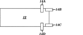
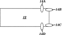
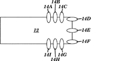
本発明のエネルギー回収器デバイスの共振器ビームの停止部構造は、様々な設計となり得る。共振器ビームと一体化されてまたはその上に形成された停止部構造のいくつかの限定されない例が、図7A〜7Lに示されている。図7Aにおいて、共振器ビーム12は、共振器ビーム12の角部から生じる2つの停止部14Aおよび14Bを備える。図7Bにおいて、共振器ビーム12上で、3つの停止部14A、14B、および14Cが使用される。図7Cにおいて、停止部14は、共振器ビーム12の3つの異なる縁部に沿って形成される。図7Dにおいて、停止部14は、共振器ビーム12の1つの縁部に沿って形成される。図7Eにおいて、停止部14Aおよび14Bは、共振器ビーム12の2つの角部に位置する。図7Fは、3つの停止部14A、14B、および14Cを示し、これらは、共振器ビーム12の3つの異なる側面から突出する個々の構造として形成される。図7Gにおいて、4つの停止部14A、14B、14C、および14Dが存在する。共振器ビーム12の第1の側面は、2つの停止部14Bおよび14Cを含み、2つの他の側面は、それぞれ単一の停止部(14Aおよび14D)を含む。図7Hは、共振器ビーム12の3つの異なる側面に沿った3つの停止部のセットとして形成される停止部14A、14B、14C、14D、14E、14F、14G、14H、および14Iを含む、いくつかの停止部を使用している。図7I、7J、7K、および7Lは、それぞれ図7E、7F、7G、および7Hに示されるものと類似した構造を有する共振器ビーム12を示すが、但し、図7I、7J、7K、および7Lにおける停止部14は、図7E、7F、7G、および7Hにおける停止部14の矩形形状と比較して、丸い形状を有する。
The resonator beam stop structure of the energy recovery device of the present invention can be of various designs. Some non-limiting examples of stop structures integrated with or formed on the resonator beam are shown in FIGS. In FIG. 7A, the
共振器ビームとは別個の構造として形成される場合、停止部は、金属、フォトレジスト、ポリイミド、SiO2、および他の相補型金属酸化物半導体適合性材料、またはそれらの任意の組み合わせからなる群から選択される材料で構築され得る。 If a resonator beam formed as a separate structure, stop is a metal, the group consisting of photoresist, polyimide, SiO 2, and other complementary metal oxide semiconductor compatible materials or any combination thereof, Can be constructed of materials selected from
一実施形態によれば、本発明のエネルギー回収器デバイスの停止部は、可撓性である。したがって、例えば、図6B〜6Cを参照して、停止部514は、振動中に壁530Aおよび530Bと接触すると、曲がって共振器ビーム512の安定化を補助する。
According to one embodiment, the stop of the energy recovery device of the present invention is flexible. Thus, for example, referring to FIGS. 6B-6C, stop 514 bends to assist in stabilizing
停止部構造は、本発明のエネルギー回収器デバイスの共振器ビーム上、および/または塊体上に形成され得る。したがって、図8に示されるように、エネルギー回収器デバイス610は、2つの停止部614Aおよび614Bを含み得る。停止部614Aは、共振器ビーム612および第1第2の端部618上に形成され、停止部614Bは、塊体622の下側に形成される。共振器ビーム612は、基部620の第1の端部616に取り付けられる。
The stop structure may be formed on the resonator beam and / or on the mass of the energy recovery device of the present invention. Thus, as shown in FIG. 8, the
図9Aおよび9Bは、部分的にパッケージ626内に封入された図8のカンチレバー構造を示した。図9Aにおいて、共振器ビーム612の第2の端部618は、共振器ビーム612の振動中に上方に屈曲し、停止部614Aは、パッケージ626の壁630Aと接触して、共振器ビーム612とパッケージ626の任意の他の部分とのいかなる接触も防止し、共振器ビーム612の動きを安定化する。図9Bにおいて、共振器ビーム612の第2の端部618は、共振器ビーム612の振動中に下方に屈曲し、停止部614Bは、パッケージ626の壁630Bと接触して、共振器ビーム612(および塊体622)とパッケージ626の任意の他の部分とのいかなる接触も防止し、共振器ビーム612の動きを安定化する。一方、共振器ビーム612の第1の端部616は、基部620に固定されたままである。停止部614Aおよび614Bは、共振器ビーム612の動きを安定化するために、エネルギー回収器デバイス610上に最適な態様で設置される。
FIGS. 9A and 9B show the cantilever structure of FIG. 8 partially encapsulated within a
本発明の別の態様は、電動装置と、電動装置に電気的に結合された本発明のエネルギー回収器デバイスとを備えるシステムに関する。 Another aspect of the invention relates to a system comprising a motorized device and the energy recovery device of the present invention electrically coupled to the motorized device.
ここで図10を参照すると、電動装置(スマートフォン)32が、(その外部筐体内に)エネルギー回収器デバイス10を含むように示されている。この実施形態によれば、エネルギー回収器デバイス10は、別の独立エネルギー源(例えば、電池)の代わりに、またはそれと併せて使用される独立エネルギー源をスマートフォン32に給電するために提供する。代替の実施形態において、電動装置は、例えば、タブレット、PC、および/またはスマートフォンと電気的に通信する腕時計型デバイスまたはネックレス等の、ウェアラブルデバイスである。
Referring now to FIG. 10, a motorized device (smartphone) 32 is shown including an energy recovery device 10 (in its external housing). According to this embodiment, the
電動装置および本発明のエネルギー回収器デバイスを含む本発明の他のシステムは、限定されることなく、ラップトップコンピュータ、タブレットコンピュータ、携帯電話、電子書籍リーダー、MP3プレーヤー、電話ヘッドセット、ヘッドフォン、ルータ、ゲームデバイス、ゲームコントローラ、モバイルインターネットアダプタ、カメラ、無線センサー、タブレット、PC、および/またはスマートフォンと通信するウェアラブルセンサー、(工業、レール、建物、農業等を監視するネットワーク用)無線センサーモート、タイヤ圧センサーモニタ、電子ディスプレイ(例えば、電動ツール上)、家畜監視用農業デバイス、医療デバイス、人体監視デバイス、ならびに玩具を含む。 Other systems of the present invention including the motorized device and the energy recovery device of the present invention include, but are not limited to, laptop computers, tablet computers, mobile phones, e-book readers, MP3 players, telephone headsets, headphones, routers , Game devices, game controllers, mobile internet adapters, cameras, wireless sensors, tablets, PCs, and / or wearable sensors that communicate with smartphones, wireless sensor motes (for networks that monitor industry, rails, buildings, agriculture, etc.), tires Includes pressure sensor monitors, electronic displays (eg, on power tools), livestock monitoring agricultural devices, medical devices, human body monitoring devices, and toys.
例えば、一実施形態によれば、本発明のシステムは、例えば、任意の1つ以上の様々な環境特性(温度、湿度、光、音、振動、風、運動等)を監視するためのセンサーを含む無線センサーデバイスである。本発明のエネルギー回収器デバイスは、センサーと結合され、センサーに電力を提供する。 For example, according to one embodiment, the system of the present invention includes sensors for monitoring any one or more of various environmental characteristics (temperature, humidity, light, sound, vibration, wind, movement, etc.), for example. Including wireless sensor devices. The energy recovery device of the present invention is coupled to a sensor and provides power to the sensor.
一例によれば、本発明のシステムは、タイヤ圧を監視するためのセンサーを含むタイヤ圧監視システムである。本発明のエネルギー回収器デバイスは、センサーに結合されて電力を提供する。そのようなシステムは、例えば、自動車のホイールまたはタイヤ上に装着される小型デバイスとして形成され得る。 According to one example, the system of the present invention is a tire pressure monitoring system that includes a sensor for monitoring tire pressure. The energy recovery device of the present invention is coupled to a sensor to provide power. Such a system can be formed, for example, as a miniature device mounted on an automobile wheel or tire.
別の例によれば、本発明のシステムは、家庭用または商業用衣類乾燥機の電子制御部と通信する湿度センサーである。本発明のエネルギー回収器デバイスは、センサーに結合されて電力を提供する。そのようなシステムは、例えば、衣類乾燥機内の湿度レベルに基づいて衣類の乾燥度を監視するために衣類乾燥機の内側に装着される小型デバイスとして形成され得る。代替として、デバイスは、衣類乾燥機の内側に装着されず、例えば、衣類と共に乾燥機内に投入され得るデバイス(例えば、ボール)である。次いで、センサーは、衣類乾燥機の電子制御部と通信して、例えば、サイクルの終了を決定することができる。 According to another example, the system of the present invention is a humidity sensor that communicates with the electronic control of a home or commercial clothes dryer. The energy recovery device of the present invention is coupled to a sensor to provide power. Such a system can be formed, for example, as a small device that is mounted inside the clothes dryer to monitor the dryness of the clothes based on the humidity level in the clothes dryer. Alternatively, the device is a device (eg, a ball) that is not attached to the inside of the clothes dryer and can be placed in the dryer with the clothes, for example. The sensor can then communicate with the electronic control of the clothes dryer to determine, for example, the end of the cycle.
本発明のさらなる態様は、電動装置に電力供給する方法に関する。この方法は、本発明のシステムを提供することと、圧電材料から電気エネルギーを生成するために、システムを運動または振動に供することと、装置に電力を提供するために、圧電材料からの電気エネルギーを装置に伝達することとを含む。 A further aspect of the invention relates to a method of supplying power to an electric device. The method provides a system of the present invention, subjecting the system to motion or vibration to generate electrical energy from the piezoelectric material, and providing electrical power to the device from the electrical energy from the piezoelectric material. Communicating to the device.
本発明の別の態様は、エネルギー回収器デバイスを製造する方法に関する。この方法は、エネルギー回収器デバイスを製造するために、第1および第2の表面を有するシリコンウェハを提供することと、シリコンウェハの第1の表面上に第1の二酸化ケイ素(SiO2)層を堆積させることと、第1の二酸化ケイ素層上にカンチレバー材料を堆積させることと、カンチレバー材料上に第2の二酸化ケイ素層を堆積させることと、第2の二酸化ケイ素層上に圧電スタック層を堆積させることと、圧電スタック層をパターニングすることと、第2の二酸化ケイ素層、カンチレバー材料、および第1の二酸化ケイ素層をパターニングすることと、シリコンウェハの第2の表面をエッチングすることとを含む。エネルギー回収器デバイスは、第1の端部と第2の端部との間に延在する細長共振器ビームと、第1の端部で共振器ビームに接続され、第2の端部はカンチレバーとして基部から自由に延在している、基部と、共振器ビームの第2の端部に取り付けられた塊体と、共振器ビームの第2の端部にあるばね先端とを備える。 Another aspect of the invention relates to a method of manufacturing an energy recovery device. The method provides a silicon wafer having first and second surfaces for manufacturing an energy recovery device and a first silicon dioxide (SiO 2 ) layer on the first surface of the silicon wafer. Depositing a cantilever material on the first silicon dioxide layer; depositing a second silicon dioxide layer on the cantilever material; and a piezoelectric stack layer on the second silicon dioxide layer. Depositing, patterning the piezoelectric stack layer, patterning the second silicon dioxide layer, the cantilever material, and the first silicon dioxide layer, and etching the second surface of the silicon wafer. Including. An energy recovery device includes an elongated resonator beam extending between a first end and a second end, and a first end connected to the resonator beam, the second end being a cantilever A base, freely extending from the base, a mass attached to the second end of the resonator beam, and a spring tip at the second end of the resonator beam.
一実施形態によれば、本発明の方法は、パターニングされた圧電スタック層、ならびにパターニングされた第2の二酸化ケイ素層、カンチレバー材料、および第1の二酸化ケイ素層の上に、第3の二酸化ケイ素層を堆積させることと、第3の二酸化ケイ素層をパターニングすることとをさらに含んでもよい。別の実施形態によれば、本発明の方法は、パターニングされた第3の二酸化ケイ素層の上に金属接着パッド層を堆積させることと、金属接着パッド層をパターニングすることとをさらに含んでもよい。 According to one embodiment, the method of the present invention comprises a patterned silicon stack layer and a third silicon dioxide layer on the patterned second silicon dioxide layer, cantilever material, and first silicon dioxide layer. It may further comprise depositing a layer and patterning the third silicon dioxide layer. According to another embodiment, the method of the present invention may further comprise depositing a metal bond pad layer on the patterned third silicon dioxide layer and patterning the metal bond pad layer. .
ここで、図11を参照すると、本発明のエネルギー回収器デバイスを製造する方法の一実施形態は、本明細書に記載のようなエネルギー回収器デバイスを形成するようにパターニングされる層状材料のスタックである、層状材料スタック50を形成することを含む。層状材料スタック50は、以下の層状材料を含む:シリコンウェハ52(第1の表面51および第2の表面53を有する)、第1の二酸化ケイ素層54、カンチレバー材料56、第2の二酸化ケイ素層58、接着層60(任意選択である)、ならびに圧電スタック層61(第1の金属層62、圧電材料層64、および第2の金属層66を備える)。
Referring now to FIG. 11, one embodiment of a method of manufacturing an energy recovery device of the present invention is a stack of layered materials that are patterned to form an energy recovery device as described herein. Forming a
図11に示されるように、本発明のエネルギー回収器デバイスを形成する方法は、第1の表面51および第2の表面53を有するシリコンウェハ52を提供することと、シリコンウェハ52の第1の表面51上に、第1の二酸化ケイ素層54を堆積させることと、第1の二酸化ケイ素層54上にカンチレバー材料56を堆積させることと、カンチレバー材料56上に第2の二酸化ケイ素層58を堆積させることと、第2の二酸化ケイ素層58上に任意選択の接着層60を堆積させることと、第2の二酸化ケイ素層58上に圧電スタック層61を堆積させることにより、層状材料スタック50を形成することを含む。
As shown in FIG. 11, the method of forming the energy recovery device of the present invention provides a
シリコンウェハ52は、一実施形態によれば、単結晶両面研磨シリコンウェハである。一実施形態において、シリコンウェハ52は、約400μmから約1,000μm、約500μmから約900μm、約600μmから約800μm、または約700μmの厚さを有する。1つの具体例において、シリコンウェハ52は、約725μm(+/−15μm)の厚さ(すなわち、8インチウェハの標準厚さ)を有する両面研磨シリコンウェハである。代替として、シリコンウェハ52の代わりに、本発明の方法は、二酸化ケイ素の堆積層から開始して、その上に層状材料スタック50の後続の層が形成されてもよい。
The
第1の二酸化ケイ素層54は、一実施形態によれば、熱酸化物層である。二酸化ケイ素層54は、カンチレバー材料56を解放し、また塊体がシリコンで作製される場合には塊体も画定する、背面エッチング停止部のためのエッチング停止部を提供する。一実施形態において、第1の二酸化ケイ素層54は、約0.25μmから約2μmの厚さを有する。シリコンウェハ52への第1の二酸化ケイ素層54の堆積は、当該技術分野において知られている方法により行うことができる。例えば、二酸化ケイ素を熱成長させ、次いでシリコンウェハ上に堆積させてもよい。1つの具体例において、1μm(+/−0.05μm)の熱成長SiO2がシリコンウェハ52上に堆積し、二酸化ケイ素層54が形成される。
The first
カンチレバー材料56は、シリコン、ポリSi、金属(例えば、CuもしくはNi)、または他の金属酸化物半導体(CMOS)適合性材料、あるいはポリイミド等の高温ポリマー等の任意の好適な材料であってもよい。一実施形態において、カンチレバー材料56は、約10μmから約200μm、約10μmから約75μm、または約10μmから約50μmの厚さの範囲で化学気相成長法により第1の二酸化ケイ素層54上に堆積する。堆積後、例えば化学機械研磨により、カンチレバー材料56の表面を平滑化することが望ましくなり得る。
The
第2の二酸化ケイ素層58は、一実施形態によれば、高温酸化物層である。この層は、圧電スタック層61が良好に接着し得る表面、および圧電スタック層61の下部電極をパターニングするためのエッチング停止部を提供する。一実施形態において、第2の二酸化ケイ素層58は、化学気相成長法により約1μmの厚さでカンチレバー材料56上に堆積する。
The second
圧電スタック層61が第2の二酸化ケイ素層58上に堆積し、金属/圧電材料/金属層が形成される。一実施形態によれば、圧電スタック層61は、厚さ約0.5μmから約6μm、または約2μmから約5μmの厚さを有する。第1の金属層62および第2の金属層66は、電極として適切に機能する任意の好適な金属で形成され得る。一実施形態によれば、これらの層は、モリブデンまたは白金等の同じ材料で形成される。しかしながら、層の両方が同じ材料で形成される必要はない。圧電材料層64は、上述のような任意の好適な圧電材料で形成される。一実施形態によれば、この層は、窒化アルミニウム(AlN)で形成される。
A
圧電スタック層61の堆積は、当該技術において標準的であるように、その下に薄い接着層60を用いて行うことができる。好適な接着層60は、約0.02μmから約0.05μmの層厚のチタン、AlN、Al:Cu、またはAl等の材料を含み得る。
Deposition of the
本発明のエネルギー回収器デバイスを作製する方法の一実施形態は、図12〜19に示されるように進行する。まず、図12〜13に示されるように、圧電スタック層61がパターニングされる。特に、圧電材料層64および第2の金属層66の一部(例えば、部分68および70)が、スタック50から除去され、第1の金属層62が露出される。
One embodiment of the method of making the energy recovery device of the present invention proceeds as shown in FIGS. First, as shown in FIGS. 12 to 13, the
本発明の方法に従う圧電スタック層61のパターニングは、金属層に対するリン酸、および水酸化テトラメチルアンモニウムを用いた湿式エッチングと組み合わせた、リソグラフィー技術を使用して達成され得る。層の湿式または乾式エッチングのための他の好適な化学物質もまた、当業者により一般的に使用され、本発明の方法の実行に使用され得る。
Patterning of the
一実施形態によれば、圧電スタック層61のパターニングは、第2の金属層66および圧電材料層64の一部を除去することと、第1の金属層62をパターニングして、その一部(例えば、部分72)を除去し、そのさらなる部分を電極として露出したままとすることとを含む。電極のパターニングは、リン酸湿式エッチング、または塩素もしくはフッ素ガスを用いたプラズマ(乾式)エッチングを使用して実行され得る。接着層が存在する場合、接着層は、湿式エッチングに基づくアンモニア過酸化物により除去され得る(例えば、チタン接着層の場合)。圧電スタック層61のパターニングのこの実施形態の得られた生成物の上面図が図17に示されているが、電極24は露出するように示されている。
According to one embodiment, the patterning of the
次に、第2の二酸化ケイ素層58、カンチレバー材料56、および第1の二酸化ケイ素層54がパターニングされる。この方法ステップは、図14に示されている。一実施形態によれば、二酸化ケイ素層58、カンチレバー材料56、および第1の二酸化ケイ素層54のパターニングは、第2の二酸化ケイ素層58の一部、カンチレバー材料56の一部、および第1の二酸化ケイ素層54の一部を除去して、シリコンウェハ52の第1の表面51の部分78を露出したままとすることを含む。
Next, the second
第2の二酸化ケイ素層58、カンチレバー材料56、および第1の二酸化ケイ素層54のパターニングは、第2の二酸化ケイ素層58、カンチレバー材料56、および第1の二酸化ケイ素層54の対置する側壁を除去して、側壁を有するカンチレバー材料を形成することをさらに含んでもよい。
The patterning of the second
一実施形態によれば、このパターニングは全て、乾燥プロセスにより行われてもよい。例えば、酸化物の場合フッ素CHF3/CF4ガスおよび反応性イオンエッチング、ポリSiの場合SF6/C4F8深掘り反応性イオンエッチングがある。Cu、Au、またはNi等の金属の場合、当該技術分野において周知の湿式エッチングプロセスを使用することができる。代替として、Cu、Ni、またはAuが、シリコン層のパターニングの後に電気めっきにより追加される。 According to one embodiment, all this patterning may be performed by a drying process. For example, there is fluorine CHF 3 / CF 4 gas and reactive ion etching in the case of oxide, and SF 6 / C 4 F 8 deep reactive ion etching in the case of poly-Si. For metals such as Cu, Au, or Ni, wet etching processes well known in the art can be used. Alternatively, Cu, Ni, or Au is added by electroplating after the patterning of the silicon layer.
図15に示されるさらなる(任意選択の)方法ステップにおいて、パターニングされた圧電スタック層61、ならびにパターニングされた第2の二酸化ケイ素層58、カンチレバー材料56、および第1の二酸化ケイ素層54の上に、第3の二酸化ケイ素層59を堆積させる。一実施形態によれば、このステップは、パッシベーション層用のケイ素を堆積させるために、シラン(ケイ素源)のプラズマ化学気相成長法を使用して行われる。この層は、約1μmの厚さまで堆積し得る。別の実施形態によれば、第3の二酸化ケイ素層の堆積は、磨耗に対する堅牢性を構造に提供する任意選択のステップである。
In a further (optional) method step shown in FIG. 15, over the patterned
図16に示される次の方法ステップにおいて、存在する場合には、第3の二酸化ケイ素層59がパターニングされる。一実施形態によれば、このステップは、第3の二酸化ケイ素層59の一部を除去して、圧電スタック層61の部分68および69ならびにシリコンウェハの部分78を露出したままとすることを含む。一実施形態によれば、このパターニングは、CHF3反応性イオンエッチングプロセスを使用して行われる。
In the next method step shown in FIG. 16, the third
さらなる(任意選択の)方法ステップが図17に示されるが、これは、パターニングされた第3の二酸化ケイ素層59、ならびに圧電スタック層61の部分68およびシリコンウェハ52の部分78の上に堆積した、金属接着パッド層80を示している。接着パッド層80は、堅牢なワイヤボンドがデバイスに形成されることを可能にする表面を提供し、それにより、良好な電気接続を確実にする。一実施形態によれば、金属接着パッド層80は、約1μmの厚さまで堆積し、また金属材料(例えば、Al)である。この層は、ワイヤボンドの信頼性を改善するために堆積させる。
Further (optional) method steps are shown in FIG. 17, which were deposited on the patterned third
図18は、存在する場合には金属接着パッド層80をパターニングすることを含む次の方法ステップを示す。一実施形態によれば、金属接着パッド層80は、上部および下部電極接続用の開口部よりも若干長くパターニングされる。一実施形態において、金属接着パッド層80のパターニングは、リン酸に基づく湿潤エッチング化学を使用して行われる。しかしながら、他の方法もまた使用され得る。
FIG. 18 illustrates the next method step including patterning the metal
次の方法ステップは、図19に示されるが、シリコンウェハ52が表面53でエッチングされて共振器ビーム12、基部20、塊体22、および停止部14を形成し、このようにして本発明のエネルギー回収デバイスの一実施形態が製造される。換言すれば、シリコンウェハ52の一部がエッチング除去されて、共振器ビーム12となったものの下に穴82を形成し、基部20となったシリコンウェハ52の一部と、塊体22となったシリコンウェハ52の一部との間に間隔を形成する。同様に、シリコンウェハ52の一部がエッチング除去されて、塊体52の縁部を越えて延在する共振器ビーム12である停止部14を形成する。一実施形態によれば、シリコンウェハ52のエッチングは、リソグラフィー技術およびSF6/C4F8化学による深掘り反応性イオンエッチングを使用して行われる。
The next method step is shown in FIG. 19, in which a
本発明のさらなる態様は、エネルギー回収器デバイスを製造する方法に関する。この方法は、第1および第2の表面を有するシリコンウェハを提供することと、シリコンウェハの第1の表面上に第1の二酸化ケイ素層を堆積させることと、第1の二酸化ケイ素層上にカンチレバー材料を堆積させることと、カンチレバー材料上に第2の二酸化ケイ素層を堆積させることと、第2の二酸化ケイ素層上に圧電スタックを堆積させることと、圧電スタック層をパターニングすることと、第2の二酸化ケイ素層、カンチレバー材料、および第1の二酸化ケイ素層をパターニングすることと、エネルギー回収器デバイスを画定するために、シリコンウェハの第2の表面をエッチングすることとを含む。エネルギー回収器デバイスは、第1の端部と第2の端部との間に延在する細長共振器ビームと、第1の端部で共振器ビームに接続され、第2の端部はカンチレバーとして基部から自由に延在している、基部と、共振器ビームの第2の端部に取り付けられた塊体とを備える。方法は、停止部材料を堆積させることと、細長共振器ビームの第2の端部で停止部を画定するために、停止部材料をエッチングすることとをさらに含む。 A further aspect of the invention relates to a method of manufacturing an energy recovery device. The method provides a silicon wafer having first and second surfaces, deposits a first silicon dioxide layer on the first surface of the silicon wafer, and on the first silicon dioxide layer. Depositing a cantilever material; depositing a second silicon dioxide layer on the cantilever material; depositing a piezoelectric stack on the second silicon dioxide layer; patterning the piezoelectric stack layer; Patterning the two silicon dioxide layers, the cantilever material, and the first silicon dioxide layer, and etching the second surface of the silicon wafer to define an energy recovery device. An energy recovery device includes an elongated resonator beam extending between a first end and a second end, and a first end connected to the resonator beam, the second end being a cantilever A base extending freely from the base and a mass attached to the second end of the resonator beam. The method further includes depositing a stop material and etching the stop material to define the stop at the second end of the elongated resonator beam.
本発明のこの方法を実行する際、図12〜18に示されるのと同じステップが行われる。次のプロセスステップは、図20に示されるが、シリコンウェハ52が表面53でエッチングされて共振器ビーム12、基部20、および塊体22を形成する。換言すれば、シリコンウェハ52の一部がエッチング除去されて、共振器ビーム12となったものの下に穴82を形成し、基部20となったシリコンウェハ52の一部と、塊体22となったシリコンウェハ52の一部との間に間隔を形成する。図19に示されるものとは対照的に、このステップは、シリコンウェハ52の一部をエッチング除去して停止部14を形成することを、この段階では含まない。
In carrying out this method of the present invention, the same steps as shown in FIGS. The next process step is shown in FIG. 20, where a
その代わり、プロセスは図21に示されるように続き、このプロセスは、一実施形態によればフォトレジストラミネートまたはポリマーラミネートであるラミネート材料86を、存在する場合には接着パッド層80、または圧電スタック層61の上の構造上に堆積させることを含む。
Instead, the process continues as shown in FIG. 21, which includes a
次のプロセスステップは、ラミネート材料86をエッチングして、塊体22の上に停止部14Aを形成することを含む。
The next process step includes etching the
一実施形態によれば、塊体の下にも停止部が形成されてもよい。これは、図23〜24に示されるように実行され得る。具体的には、図23に示されるように、ラミネート材料88は、構造の下側(すなわち、塊体22の下、および必要に応じて基部20の下)に堆積させる。図24に示されるように、ラミネート材料88は、塊体22の下に停止部14Bを形成するようにエッチングされる。
According to one embodiment, a stop may also be formed under the mass. This can be performed as shown in FIGS. Specifically, as shown in FIG. 23, the
本発明のこの態様に従い塊体のいずれかの側で停止部を画定するための他の選択肢は、限定されることなく、有機もしくは無機材料のインクジェット、または金属の電気めっき等の物理的堆積を含む。 Other options for defining stops on either side of the mass in accordance with this aspect of the invention include, but are not limited to, physical deposition such as inkjet of organic or inorganic materials, or electroplating of metal. Including.
以下の実施例は、本発明の実施形態を例示するために提供されるが、決してその範囲を限定することを意図しない。 The following examples are provided to illustrate embodiments of the invention but are not intended to limit its scope in any way.
実施例1−一体化されたばね先端停止部を有するエネルギー回収器デバイス
3,146μmの長さのカンチレバー×20μmの厚さのポリシリコンカンチレバー材料、4,000μmの長さ×725μmの厚さの塊体、ならびに1,000μmの長さおよび対応する20μmの厚さのポリシリコン材料のカンチレバーの端部上のばね先端停止部を有する本発明のエネルギー回収器デバイスを、カンチレバーの上および下に1mmの空洞深さを有する空洞アセンブリ内に設置した。次いで、アセンブリを振動源の上に設置し、120Hzの共振周波数に変化させた。カンチレバーの先端は、0.54Gの加速で、カンチレバーに損傷を与えずに空洞の上部にぶつかり始めた。アセンブリは、同じ構成において3Gまでの高い加速で振動したが、カンチレバーおよびばね先端への損傷は観察されなかった。
Example 1 Energy Recovery Device with Integrated Spring Tip Stop 3,146 μm long cantilever × 20 μm thick polysilicon cantilever material, 4,000 μm long × 725 μm thick mass And an energy recovery device of the present invention having a spring tip stop on the end of a cantilever of a length of 1,000 μm and a corresponding thickness of 20 μm of polysilicon material, a 1 mm cavity above and below the cantilever Installed in a cavity assembly with depth. The assembly was then placed on a vibration source and changed to a resonant frequency of 120 Hz. The tip of the cantilever began to hit the top of the cavity at 0.54G acceleration without damaging the cantilever. The assembly oscillated with high acceleration up to 3G in the same configuration, but no damage to the cantilever and spring tip was observed.
2mm空洞に対しても同じ実験を繰り返した。デバイスは、0.75Gの加速でパッケージの上部にぶつかり始めたが、破損は観察されなかった。さらに、デバイスが3Gの加速で振動した際にも、破損は観測されなかった。 The same experiment was repeated for a 2 mm cavity. The device began to bump into the top of the package with an acceleration of 0.75G, but no breakage was observed. Furthermore, no damage was observed when the device vibrated at 3G acceleration.
本明細書(任意の添付の特許請求の範囲、要約および図面を含む)に記載の特徴の全て、ならびに/またはそのように開示された任意の方法もしくはプロセスのステップの全ては、そのような特徴および/またはステップの少なくともいくつかが相互に排他的である組み合わせを除いて、任意の組み合わせとして上述の態様のいずれかと組み合わされてもよい。 All of the features described in this specification (including any appended claims, abstract and drawings) and / or any of the steps of any method or process so disclosed are such features. And / or any combination may be combined with any of the above-described aspects, except combinations where at least some of the steps are mutually exclusive.
Claims (60)
前記第1の端部で前記共振器ビームに接続され、前記第2の端部はカンチレバーとして前記基部から自由に延在している、基部と、
前記共振器ビームの前記第2の端部に取り付けられた塊体と、
前記共振器ビームの前記第2の端部の少なくとも一部を包囲するパッケージと、
前記塊体および/または前記共振器ビームの前記第2の端部に接続され、破損を防止するために前記共振器ビームの動きを安定化するように構成された停止部と
を備える、エネルギー回収器デバイス。 An elongated resonator beam comprising a piezoelectric material and extending between a first end and a second end;
A base connected to the resonator beam at the first end and the second end freely extending from the base as a cantilever;
A mass attached to the second end of the resonator beam;
A package surrounding at least a portion of the second end of the resonator beam;
Energy recovery comprising a stop connected to the second end of the mass and / or the resonator beam and configured to stabilize movement of the resonator beam to prevent breakage Device.
をさらに備える、前記請求項のいずれか一項に記載のデバイス。 The device of any one of the preceding claims, further comprising one or more electrodes in electrical contact with the piezoelectric material.
をさらに備える、請求項11または請求項12に記載のデバイス。 13. The device of claim 11 or claim 12, further comprising an electrical recovery circuit electrically connected to the one or more electrodes for recovering electrical energy from the piezoelectric material.
前記装置に電気的に結合された請求項1に記載のデバイスと
を備える、システム。 An electric device;
A device comprising: the device of claim 1 electrically coupled to the apparatus.
をさらに備える、請求項15から25のいずれか一項に記載のシステム。 26. A system according to any one of claims 15 to 25, further comprising one or more electrodes in electrical contact with the piezoelectric material.
をさらに備える、請求項26または請求項27に記載のシステム。 28. A system according to claim 26 or claim 27, further comprising an electrical recovery circuit electrically connected to the one or more electrodes for recovering electrical energy from the piezoelectric material.
前記圧電材料から電気エネルギーを生成するために、前記システムを運動または振動に供することと、
電動装置に電力を提供するために、前記圧電材料から前記装置に前記電気エネルギーを伝達することと
を含む、電動装置に電力供給する方法。 Providing a system according to any one of claims 15 to 29;
Subjecting the system to motion or vibration to generate electrical energy from the piezoelectric material;
A method of powering an electric device, comprising: transferring the electrical energy from the piezoelectric material to the device to provide electric power to the electric device.
前記圧電材料と電気的に接触した1つ以上の電極
をさらに備える、請求項30から40のいずれか一項に記載の方法。 The system
41. The method according to any one of claims 30 to 40, further comprising one or more electrodes in electrical contact with the piezoelectric material.
前記圧電材料から電気エネルギーを回収するための、前記1つ以上の電極と電気的に接続された電気回収回路
をさらに備える、請求項41または請求項42に記載の方法。 The system
43. The method of claim 41 or claim 42, further comprising an electrical recovery circuit electrically connected to the one or more electrodes for recovering electrical energy from the piezoelectric material.
前記シリコンウェハの前記第1の表面上に第1の二酸化ケイ素層を堆積させることと、
前記第1の二酸化ケイ素層上にカンチレバー材料を堆積させることと、
前記カンチレバー材料上に第2の二酸化ケイ素層を堆積させることと、
前記第2の二酸化ケイ素層上に圧電スタックを堆積させることと、
前記圧電スタック層をパターニングすることと、
前記第2の二酸化ケイ素層、前記カンチレバー材料、および前記第1の二酸化ケイ素層をパターニングすることと、
第1の端部と第2の端部との間に延在する細長共振器ビームと、
前記第1の端部で前記共振器ビームに接続され、前記第2の端部はカンチレバーとして前記基部から自由に延在している、基部と、
前記共振器ビームの前記第2の端部に取り付けられた塊体と、
前記共振器ビームの前記第2の端部にあるばね先端と
を備えるエネルギー回収デバイスを製造するために、前記シリコンウェハの前記第2の表面をエッチングすることと
を含む、エネルギー回収デバイスを製造する方法。 Providing a silicon wafer having first and second surfaces;
Depositing a first silicon dioxide layer on the first surface of the silicon wafer;
Depositing a cantilever material on the first silicon dioxide layer;
Depositing a second silicon dioxide layer on the cantilever material;
Depositing a piezoelectric stack on the second silicon dioxide layer;
Patterning the piezoelectric stack layer;
Patterning the second silicon dioxide layer, the cantilever material, and the first silicon dioxide layer;
An elongated resonator beam extending between the first end and the second end;
A base connected to the resonator beam at the first end and the second end freely extending from the base as a cantilever;
A mass attached to the second end of the resonator beam;
Etching the second surface of the silicon wafer to manufacture an energy recovery device comprising a spring tip at the second end of the resonator beam. Method.
前記第1の金属層および圧電材料層の一部を除去することと、
前記第2の金属層の一部を除去するためおよびさらなる部分を電極として露出したままとするために、前記第2の金属層をパターニングすることと
を含む、請求項45から47のいずれか一項に記載の方法。 Patterning the piezoelectric stack layer comprises:
Removing a portion of the first metal layer and the piezoelectric material layer;
48. The method of claim 45, further comprising patterning the second metal layer to remove a portion of the second metal layer and leave a further portion exposed as an electrode. The method according to item.
前記シリコンウェハの第1の表面の一部を露出したままとするために、前記第2の二酸化ケイ素層の一部、前記カンチレバー材料の一部、および前記第1の二酸化ケイ素層の一部を除去すること
を含む、請求項45から48のいずれか一項に記載の方法。 Patterning the second silicon dioxide layer, the cantilever material, and the first silicon dioxide layer;
In order to leave a portion of the first surface of the silicon wafer exposed, a portion of the second silicon dioxide layer, a portion of the cantilever material, and a portion of the first silicon dioxide layer 49. A method according to any one of claims 45 to 48, comprising removing.
前記第3の二酸化ケイ素層をパターニングすることと、
前記パターニングされた第3の二酸化ケイ素層の上に金属接着パッド層を堆積させることと、
前記金属接着パッド層をパターニングすることと
をさらに含む、請求項45から49のいずれか一項に記載の方法。 Depositing a third silicon dioxide layer over the patterned piezoelectric stack layer and the patterned second silicon dioxide layer, the cantilever material, and the first silicon dioxide layer;
Patterning the third silicon dioxide layer;
Depositing a metal bond pad layer over the patterned third silicon dioxide layer;
50. The method of any one of claims 45 to 49, further comprising patterning the metal bond pad layer.
前記圧電スタックの一部および前記シリコンウェハの一部を露出したままとするために、前記第3の二酸化ケイ素層の一部を除去すること
を含む、請求項45から50のいずれか一項に記載の方法。 Patterning the third silicon dioxide layer comprises:
51. The method of any one of claims 45 to 50, comprising removing a portion of the third silicon dioxide layer to leave a portion of the piezoelectric stack and a portion of the silicon wafer exposed. The method described.
前記シリコンウェハの前記第1の表面上に第1の二酸化ケイ素層を堆積させることと、
前記第1の二酸化ケイ素層上にカンチレバー材料を堆積させることと、
前記カンチレバー材料上に第2の二酸化ケイ素層を堆積させることと、
前記第2の二酸化ケイ素層上に圧電スタックを堆積させることと、
前記圧電スタック層をパターニングすることと、
前記第2の二酸化ケイ素層、前記カンチレバー材料、および前記第1の二酸化ケイ素層をパターニングすることと、
第1の端部と第2の端部との間に延在する細長共振器ビームと、
前記第1の端部で前記共振器ビームに接続され、前記第2の端部はカンチレバーとして前記基部から自由に延在している、基部と、
前記共振器ビームの前記第2の端部に取り付けられた塊体と
を備えるエネルギー回収デバイスを画定するために、前記シリコンウェハの前記第2の表面をエッチングすることと、
停止部材料を堆積させることと、
前記細長共振器ビームの前記第2の端部で停止部を画定するために、前記停止部材料をエッチングすることと
を含む、エネルギー回収デバイスを製造する方法。 Providing a silicon wafer having first and second surfaces;
Depositing a first silicon dioxide layer on the first surface of the silicon wafer;
Depositing a cantilever material on the first silicon dioxide layer;
Depositing a second silicon dioxide layer on the cantilever material;
Depositing a piezoelectric stack on the second silicon dioxide layer;
Patterning the piezoelectric stack layer;
Patterning the second silicon dioxide layer, the cantilever material, and the first silicon dioxide layer;
An elongated resonator beam extending between the first end and the second end;
A base connected to the resonator beam at the first end and the second end freely extending from the base as a cantilever;
Etching the second surface of the silicon wafer to define an energy recovery device comprising a mass attached to the second end of the resonator beam;
Depositing stop material;
Etching the stop material to define a stop at the second end of the elongated resonator beam.
前記第1の金属層および圧電材料層の一部を除去することと、
前記第2の金属層の一部を除去するためおよびさらなる部分を電極として露出したままとするために、前記第2の金属層をパターニングすることと
を含む、請求項52から54のいずれか一項に記載の方法。 Patterning the piezoelectric stack layer comprises:
Removing a portion of the first metal layer and the piezoelectric material layer;
55. The method according to any one of claims 52 to 54, comprising patterning the second metal layer to remove a portion of the second metal layer and to leave a further portion exposed as an electrode. The method according to item.
前記シリコンウェハの前記第1の表面の一部を露出したままとするために、前記第2の二酸化ケイ素層の一部、前記カンチレバー材料の一部、および前記第1の二酸化ケイ素層の一部を除去すること
を含む、請求項52から55のいずれか一項に記載の方法。 Patterning the second silicon dioxide layer, the cantilever material, and the first silicon dioxide layer;
A portion of the second silicon dioxide layer, a portion of the cantilever material, and a portion of the first silicon dioxide layer to leave a portion of the first surface of the silicon wafer exposed. 56. A method according to any one of claims 52 to 55, comprising removing.
前記第3の二酸化ケイ素層をパターニングすることと、
前記パターニングされた第3の二酸化ケイ素層の上に金属接着パッド層を堆積させることと、
前記金属接着パッド層をパターニングすることと
をさらに含む、請求項52から56のいずれか一項に記載の方法。 Depositing a third silicon dioxide layer over the patterned piezoelectric stack layer and the patterned second silicon dioxide layer, the cantilever material, and the first silicon dioxide layer;
Patterning the third silicon dioxide layer;
Depositing a metal bond pad layer over the patterned third silicon dioxide layer;
57. The method of any one of claims 52 to 56, further comprising patterning the metal bond pad layer.
前記圧電スタックの一部および前記シリコンウェハの一部を露出したままとするために、前記第3の二酸化ケイ素層の一部を除去すること
を含む、請求項57に記載の方法。 Patterning the third silicon dioxide layer comprises:
58. The method of claim 57, comprising removing a portion of the third silicon dioxide layer to leave a portion of the piezoelectric stack and a portion of the silicon wafer exposed.
Applications Claiming Priority (3)
| Application Number | Priority Date | Filing Date | Title |
|---|---|---|---|
| US201361780247P | 2013-03-13 | 2013-03-13 | |
| US61/780,247 | 2013-03-13 | ||
| PCT/US2013/078520 WO2014143373A1 (en) | 2013-03-13 | 2013-12-31 | Piezoelectric energy harvester device with stopper structure |
Publications (2)
| Publication Number | Publication Date |
|---|---|
| JP2016517684A true JP2016517684A (en) | 2016-06-16 |
| JP2016517684A5 JP2016517684A5 (en) | 2017-02-02 |
Family
ID=51537486
Family Applications (1)
| Application Number | Title | Priority Date | Filing Date |
|---|---|---|---|
| JP2016500152A Pending JP2016517684A (en) | 2013-03-13 | 2013-12-31 | Piezoelectric energy recovery device with stop structure |
Country Status (6)
| Country | Link |
|---|---|
| US (1) | US9479089B2 (en) |
| EP (1) | EP2971761A4 (en) |
| JP (1) | JP2016517684A (en) |
| KR (1) | KR20150130972A (en) |
| CA (1) | CA2892278A1 (en) |
| WO (1) | WO2014143373A1 (en) |
Cited By (2)
| Publication number | Priority date | Publication date | Assignee | Title |
|---|---|---|---|---|
| JP6389023B1 (en) * | 2017-07-26 | 2018-09-12 | 株式会社トライフォース・マネジメント | Power generation element |
| JP2021020667A (en) * | 2019-07-24 | 2021-02-18 | Tdk株式会社 | Smart wheel energy harvester |
Families Citing this family (7)
| Publication number | Priority date | Publication date | Assignee | Title |
|---|---|---|---|---|
| WO2014141557A1 (en) * | 2013-03-13 | 2014-09-18 | 東海ゴム工業株式会社 | Power generator |
| EP3038247A4 (en) * | 2013-08-16 | 2017-05-10 | AMC ENERGY CO., Ltd. | Piezoelectric harvesting system using repulsion force |
| WO2015087537A1 (en) * | 2013-12-12 | 2015-06-18 | パナソニックIpマネジメント株式会社 | Vibration power-generation device, vibration monitoring device and system |
| ES2890451T3 (en) * | 2015-03-27 | 2022-01-19 | Saronikos Trading & Services Unipessoal Lda | Electronic wristwatch or pocket watch comprising a rotating crown |
| KR102234578B1 (en) * | 2015-04-21 | 2021-03-31 | (주)와이솔 | Piezoelectric vibration module |
| DE102017200111B3 (en) * | 2017-01-05 | 2018-03-15 | Robert Bosch Gmbh | Micromechanical sound transducer arrangement and corresponding production method |
| CN109587612A (en) * | 2018-12-31 | 2019-04-05 | 瑞声声学科技(深圳)有限公司 | Piezoelectric microphone |
Citations (4)
| Publication number | Priority date | Publication date | Assignee | Title |
|---|---|---|---|---|
| JP2003218418A (en) * | 2002-01-18 | 2003-07-31 | Matsushita Electric Ind Co Ltd | Piezoelectric power generator |
| JP2006216898A (en) * | 2005-02-07 | 2006-08-17 | Nec Tokin Corp | Piezoelectric generator |
| US20110140579A1 (en) * | 2009-12-14 | 2011-06-16 | Electronics And Telecommunications Research Institute | Active piezoelectric energy harvester with embedded variable capacitance layer and method of manufacturing the same |
| JP2011160576A (en) * | 2010-02-02 | 2011-08-18 | Seiko Epson Corp | Piezoelectric power generator |
Family Cites Families (34)
| Publication number | Priority date | Publication date | Assignee | Title |
|---|---|---|---|---|
| GB1363215A (en) * | 1973-01-04 | 1974-08-14 | Mullard Ltd | Mechanical-electrical transducer |
| CH626479A5 (en) | 1979-07-05 | 1981-11-13 | Suisse Horlogerie | |
| US4906840A (en) * | 1988-01-27 | 1990-03-06 | The Board Of Trustees Of Leland Stanford Jr., University | Integrated scanning tunneling microscope |
| US5708320A (en) * | 1994-10-28 | 1998-01-13 | Alps Electric Co., Ltd | Vibratory gyroscope |
| DE4445177C5 (en) | 1994-11-22 | 2015-09-17 | Fraunhofer-Gesellschaft zur Förderung der angewandten Forschung e.V. | Method for producing micromechanical components with free-standing microstructures |
| US5646583A (en) | 1996-01-04 | 1997-07-08 | Rockwell International Corporation | Acoustic isolator having a high impedance layer of hafnium oxide |
| US6396201B1 (en) | 1997-08-19 | 2002-05-28 | Miyota Co., Ltd. | Piezoelectric vibrator |
| US6078126A (en) * | 1998-05-29 | 2000-06-20 | Motorola, Inc. | Resonant piezoelectric alerting device |
| JP3845544B2 (en) | 1999-10-01 | 2006-11-15 | 日本碍子株式会社 | Piezoelectric / electrostrictive device and manufacturing method thereof |
| JP2003037312A (en) * | 2001-07-23 | 2003-02-07 | Matsushita Electric Ind Co Ltd | Stress sensor |
| US7181977B2 (en) * | 2002-01-22 | 2007-02-27 | Measurement Specialties, Inc. | Sensor assembly with lead attachment |
| DE10221420A1 (en) * | 2002-05-14 | 2003-12-11 | Enocean Gmbh | Device for converting mechanical energy into electrical energy |
| US7270952B2 (en) | 2002-09-24 | 2007-09-18 | Intel Corporation | Detecting molecular binding by monitoring feedback controlled cantilever deflections |
| US6858970B2 (en) | 2002-10-21 | 2005-02-22 | The Boeing Company | Multi-frequency piezoelectric energy harvester |
| US20050134149A1 (en) | 2003-07-11 | 2005-06-23 | Deng Ken K. | Piezoelectric vibration energy harvesting device |
| US7397169B2 (en) * | 2004-03-19 | 2008-07-08 | Lawrence Livermore National Security, Llc | Energy harvesting using a thermoelectric material |
| US7596841B2 (en) | 2004-04-23 | 2009-10-06 | Agency For Science Technology And Research | Micro-electromechanical devices and methods of fabricating thereof |
| US7692365B2 (en) * | 2005-11-23 | 2010-04-06 | Microstrain, Inc. | Slotted beam piezoelectric composite |
| US20070125176A1 (en) | 2005-12-02 | 2007-06-07 | Honeywell International, Inc. | Energy harvesting device and methods |
| US8030807B2 (en) * | 2005-12-09 | 2011-10-04 | Chubb International Holdings Limited | Electromechanical energy harvesting system |
| DE102006037692A1 (en) * | 2006-08-11 | 2008-02-14 | Robert Bosch Gmbh | circuit module |
| US7839058B1 (en) * | 2007-01-29 | 2010-11-23 | Microstrain, Inc. | Wideband vibration energy harvester |
| US8080920B2 (en) | 2007-03-21 | 2011-12-20 | The University Of Vermont And State Agricultural College | Piezoelectric vibrational energy harvesting systems incorporating parametric bending mode energy harvesting |
| US7893599B2 (en) | 2008-01-29 | 2011-02-22 | Washington State University | Energy converters and associated methods |
| EP2109217A3 (en) | 2008-04-07 | 2013-05-15 | Stichting IMEC Nederland | System and method for resonance frequency tuning of resonant devices |
| US8222754B1 (en) * | 2008-05-28 | 2012-07-17 | Arjae Spectral Enterprises Ltd. | Vibration-based power generator |
| US20110264293A1 (en) | 2010-04-27 | 2011-10-27 | Earl David Forrest | System and method of determining an energy harvesting capability of a location |
| US8479363B2 (en) | 2010-05-11 | 2013-07-09 | Hao Zhang | Methods for wafer level trimming of acoustically coupled resonator filter |
| US20120049694A1 (en) | 2010-08-27 | 2012-03-01 | Stichting Imec Nederland | Micromachined Piezoelectric Energy Harvester with Polymer Beam |
| US9054294B2 (en) * | 2011-10-06 | 2015-06-09 | Texas Instruments Incorporated | Soft mechanical stops to limit over-travel of proof masses in cantilevered piezoelectric devices |
| US8866316B2 (en) | 2012-06-21 | 2014-10-21 | General Electric Company | Tunable vibration energy harvester and method |
| CA2892267A1 (en) | 2013-03-13 | 2014-10-09 | Microgen Systems, Inc. | Symmetric dual piezoelectric stack microelectromechanical piezoelectric cantilever energy harvester |
| WO2014141557A1 (en) * | 2013-03-13 | 2014-09-18 | 東海ゴム工業株式会社 | Power generator |
| US9728707B2 (en) * | 2014-02-05 | 2017-08-08 | Microgen Systems, Inc. | Packaged piezoelectric energy harvester device with a compliant stopper structure, system, and methods of use and making |
-
2013
- 2013-12-31 CA CA2892278A patent/CA2892278A1/en not_active Abandoned
- 2013-12-31 JP JP2016500152A patent/JP2016517684A/en active Pending
- 2013-12-31 US US14/145,560 patent/US9479089B2/en not_active Expired - Fee Related
- 2013-12-31 KR KR1020157019541A patent/KR20150130972A/en not_active Application Discontinuation
- 2013-12-31 EP EP13877574.7A patent/EP2971761A4/en not_active Withdrawn
- 2013-12-31 WO PCT/US2013/078520 patent/WO2014143373A1/en active Application Filing
Patent Citations (4)
| Publication number | Priority date | Publication date | Assignee | Title |
|---|---|---|---|---|
| JP2003218418A (en) * | 2002-01-18 | 2003-07-31 | Matsushita Electric Ind Co Ltd | Piezoelectric power generator |
| JP2006216898A (en) * | 2005-02-07 | 2006-08-17 | Nec Tokin Corp | Piezoelectric generator |
| US20110140579A1 (en) * | 2009-12-14 | 2011-06-16 | Electronics And Telecommunications Research Institute | Active piezoelectric energy harvester with embedded variable capacitance layer and method of manufacturing the same |
| JP2011160576A (en) * | 2010-02-02 | 2011-08-18 | Seiko Epson Corp | Piezoelectric power generator |
Cited By (7)
| Publication number | Priority date | Publication date | Assignee | Title |
|---|---|---|---|---|
| JP6389023B1 (en) * | 2017-07-26 | 2018-09-12 | 株式会社トライフォース・マネジメント | Power generation element |
| WO2019021400A1 (en) * | 2017-07-26 | 2019-01-31 | 株式会社 トライフォース・マネジメント | Power generation element |
| US11205977B2 (en) | 2017-07-26 | 2021-12-21 | Tri-Force Management Corporation | Power generating element |
| JP2021020667A (en) * | 2019-07-24 | 2021-02-18 | Tdk株式会社 | Smart wheel energy harvester |
| JP6997259B2 (en) | 2019-07-24 | 2022-01-17 | Tdk株式会社 | Smart wheel energy harvester |
| TWI764197B (en) * | 2019-07-24 | 2022-05-11 | 日商Tdk股份有限公司 | Energy harvester system and a method for energy harvesting |
| US11791748B2 (en) | 2019-07-24 | 2023-10-17 | Tdk Corporation | Smart wheel energy harvester |
Also Published As
| Publication number | Publication date |
|---|---|
| WO2014143373A1 (en) | 2014-09-18 |
| EP2971761A4 (en) | 2016-08-31 |
| CA2892278A1 (en) | 2014-09-18 |
| US20150188458A1 (en) | 2015-07-02 |
| US9479089B2 (en) | 2016-10-25 |
| EP2971761A1 (en) | 2016-01-20 |
| KR20150130972A (en) | 2015-11-24 |
Similar Documents
| Publication | Publication Date | Title |
|---|---|---|
| JP2016517684A (en) | Piezoelectric energy recovery device with stop structure | |
| US9484522B2 (en) | Piezoelectric energy harvester device with curved sidewalls, system, and methods of use and making | |
| US9362480B2 (en) | Symmetric dual piezoelectric stack microelectromechanical piezoelectric cantilever energy harvester | |
| US9728707B2 (en) | Packaged piezoelectric energy harvester device with a compliant stopper structure, system, and methods of use and making | |
| JP5337721B2 (en) | Piezoelectric vibration energy harvesting system incorporating parametric bending mode energy harvesting | |
| KR100512960B1 (en) | Flexible MEMS transducer and its manufacturing method, and flexible MEMS wireless microphone | |
| US20130127295A1 (en) | Piezoelectric micro power generator and fabrication method thereof | |
| US9502635B2 (en) | Symmetric dual piezoelectric stack microelectromechanical piezoelectric devices | |
| US9293689B2 (en) | Method of manufacturing a piezoelectric micro energy harvester | |
| JP2016517684A5 (en) | ||
| JP2017506491A (en) | Packaged piezoelectric energy harvesting device, system, and method of use and fabrication having a compliant stopper structure | |
| WO2012164545A1 (en) | Energy scavenging from a rotating gear using an impact type piezoelectric mems scavenger | |
| US20160141980A1 (en) | Piezoelectric energy harvesting and signal processing system, and method of use | |
| KR101308908B1 (en) | Layered energy harvesting apparatus using nano piezo-electirc resonator and mehtod thereof | |
| KR101361824B1 (en) | Power generator using nano piezo-electric resonator and fabrication method for pad thereof | |
| CN113573218B (en) | Piezoelectric acoustic sensor and method for manufacturing the same | |
| KR20090061862A (en) | Power generating device array and system, and method for manufacturing the same | |
| WO2016076881A1 (en) | Piezoelectric energy harvesting and signal processing system, and method of use | |
| Xu et al. | Mems-based pzt/pzt bimorph thick film vibration energy harvester |
Legal Events
| Date | Code | Title | Description |
|---|---|---|---|
| A521 | Request for written amendment filed |
Free format text: JAPANESE INTERMEDIATE CODE: A523 Effective date: 20161213 |
|
| A621 | Written request for application examination |
Free format text: JAPANESE INTERMEDIATE CODE: A621 Effective date: 20161213 |
|
| A131 | Notification of reasons for refusal |
Free format text: JAPANESE INTERMEDIATE CODE: A131 Effective date: 20171016 |
|
| A977 | Report on retrieval |
Free format text: JAPANESE INTERMEDIATE CODE: A971007 Effective date: 20171018 |
|
| A601 | Written request for extension of time |
Free format text: JAPANESE INTERMEDIATE CODE: A601 Effective date: 20180115 |
|
| A02 | Decision of refusal |
Free format text: JAPANESE INTERMEDIATE CODE: A02 Effective date: 20180613 |