JP2016509128A - Method for producing a chromium coating on a metal substrate - Google Patents
Method for producing a chromium coating on a metal substrate Download PDFInfo
- Publication number
- JP2016509128A JP2016509128A JP2015552117A JP2015552117A JP2016509128A JP 2016509128 A JP2016509128 A JP 2016509128A JP 2015552117 A JP2015552117 A JP 2015552117A JP 2015552117 A JP2015552117 A JP 2015552117A JP 2016509128 A JP2016509128 A JP 2016509128A
- Authority
- JP
- Japan
- Prior art keywords
- layer
- metal substrate
- coating
- heat treatment
- depositing
- Prior art date
- Legal status (The legal status is an assumption and is not a legal conclusion. Google has not performed a legal analysis and makes no representation as to the accuracy of the status listed.)
- Granted
Links
- 239000011651 chromium Substances 0.000 title claims abstract description 98
- 238000000576 coating method Methods 0.000 title claims abstract description 97
- 239000000758 substrate Substances 0.000 title claims abstract description 83
- 239000011248 coating agent Substances 0.000 title claims abstract description 78
- 229910052751 metal Inorganic materials 0.000 title claims abstract description 75
- 239000002184 metal Substances 0.000 title claims abstract description 75
- 229910052804 chromium Inorganic materials 0.000 title claims abstract description 45
- VYZAMTAEIAYCRO-UHFFFAOYSA-N Chromium Chemical compound [Cr] VYZAMTAEIAYCRO-UHFFFAOYSA-N 0.000 title claims abstract description 43
- 238000004519 manufacturing process Methods 0.000 title claims abstract description 7
- 238000010438 heat treatment Methods 0.000 claims abstract description 82
- PXHVJJICTQNCMI-UHFFFAOYSA-N nickel Substances [Ni] PXHVJJICTQNCMI-UHFFFAOYSA-N 0.000 claims abstract description 69
- OFNHPGDEEMZPFG-UHFFFAOYSA-N phosphanylidynenickel Chemical compound [P].[Ni] OFNHPGDEEMZPFG-UHFFFAOYSA-N 0.000 claims abstract description 8
- 229910001096 P alloy Inorganic materials 0.000 claims abstract description 6
- 229910018104 Ni-P Inorganic materials 0.000 claims abstract 13
- 229910018536 Ni—P Inorganic materials 0.000 claims abstract 13
- 238000000034 method Methods 0.000 claims description 52
- 238000000151 deposition Methods 0.000 claims description 31
- 229910052759 nickel Inorganic materials 0.000 claims description 24
- 238000009713 electroplating Methods 0.000 claims description 22
- 238000005260 corrosion Methods 0.000 claims description 15
- 230000007797 corrosion Effects 0.000 claims description 15
- 229910052698 phosphorus Inorganic materials 0.000 claims description 15
- 238000007747 plating Methods 0.000 claims description 8
- OAICVXFJPJFONN-UHFFFAOYSA-N Phosphorus Chemical compound [P] OAICVXFJPJFONN-UHFFFAOYSA-N 0.000 claims description 7
- 239000011574 phosphorus Substances 0.000 claims description 7
- 229910045601 alloy Inorganic materials 0.000 claims description 5
- 239000000956 alloy Substances 0.000 claims description 5
- 238000000231 atomic layer deposition Methods 0.000 claims description 4
- 239000000919 ceramic Substances 0.000 claims description 4
- 238000005229 chemical vapour deposition Methods 0.000 claims description 4
- 238000005240 physical vapour deposition Methods 0.000 claims description 4
- 238000000427 thin-film deposition Methods 0.000 claims description 4
- 229910001092 metal group alloy Inorganic materials 0.000 claims description 3
- 238000007772 electroless plating Methods 0.000 claims description 2
- 239000010410 layer Substances 0.000 description 98
- 238000001228 spectrum Methods 0.000 description 16
- 229910000831 Steel Inorganic materials 0.000 description 15
- 239000010959 steel Substances 0.000 description 15
- 238000002441 X-ray diffraction Methods 0.000 description 13
- 239000000523 sample Substances 0.000 description 10
- 230000008021 deposition Effects 0.000 description 9
- 230000006698 induction Effects 0.000 description 9
- XEEYBQQBJWHFJM-UHFFFAOYSA-N Iron Chemical compound [Fe] XEEYBQQBJWHFJM-UHFFFAOYSA-N 0.000 description 7
- 238000001816 cooling Methods 0.000 description 5
- 229910052799 carbon Inorganic materials 0.000 description 4
- 238000000724 energy-dispersive X-ray spectrum Methods 0.000 description 4
- 239000000463 material Substances 0.000 description 4
- 239000000243 solution Substances 0.000 description 4
- OKKJLVBELUTLKV-UHFFFAOYSA-N Methanol Chemical compound OC OKKJLVBELUTLKV-UHFFFAOYSA-N 0.000 description 3
- 239000002131 composite material Substances 0.000 description 3
- 150000001875 compounds Chemical class 0.000 description 3
- 238000001341 grazing-angle X-ray diffraction Methods 0.000 description 3
- 150000002500 ions Chemical class 0.000 description 3
- 229910052742 iron Inorganic materials 0.000 description 3
- 238000004093 laser heating Methods 0.000 description 3
- 238000001000 micrograph Methods 0.000 description 3
- XLYOFNOQVPJJNP-UHFFFAOYSA-N water Substances O XLYOFNOQVPJJNP-UHFFFAOYSA-N 0.000 description 3
- 229910018072 Al 2 O 3 Inorganic materials 0.000 description 2
- 229910001369 Brass Inorganic materials 0.000 description 2
- OKTJSMMVPCPJKN-UHFFFAOYSA-N Carbon Chemical compound [C] OKTJSMMVPCPJKN-UHFFFAOYSA-N 0.000 description 2
- RYGMFSIKBFXOCR-UHFFFAOYSA-N Copper Chemical compound [Cu] RYGMFSIKBFXOCR-UHFFFAOYSA-N 0.000 description 2
- 239000010951 brass Substances 0.000 description 2
- JOPOVCBBYLSVDA-UHFFFAOYSA-N chromium(6+) Chemical compound [Cr+6] JOPOVCBBYLSVDA-UHFFFAOYSA-N 0.000 description 2
- 239000011247 coating layer Substances 0.000 description 2
- 229910052802 copper Inorganic materials 0.000 description 2
- 239000010949 copper Substances 0.000 description 2
- 239000008151 electrolyte solution Substances 0.000 description 2
- 150000002739 metals Chemical class 0.000 description 2
- BDAGIHXWWSANSR-UHFFFAOYSA-N methanoic acid Natural products OC=O BDAGIHXWWSANSR-UHFFFAOYSA-N 0.000 description 2
- 239000000203 mixture Substances 0.000 description 2
- KERTUBUCQCSNJU-UHFFFAOYSA-L nickel(2+);disulfamate Chemical compound [Ni+2].NS([O-])(=O)=O.NS([O-])(=O)=O KERTUBUCQCSNJU-UHFFFAOYSA-L 0.000 description 2
- 239000000126 substance Substances 0.000 description 2
- 238000011282 treatment Methods 0.000 description 2
- OSWFIVFLDKOXQC-UHFFFAOYSA-N 4-(3-methoxyphenyl)aniline Chemical compound COC1=CC=CC(C=2C=CC(N)=CC=2)=C1 OSWFIVFLDKOXQC-UHFFFAOYSA-N 0.000 description 1
- KWSLGOVYXMQPPX-UHFFFAOYSA-N 5-[3-(trifluoromethyl)phenyl]-2h-tetrazole Chemical compound FC(F)(F)C1=CC=CC(C2=NNN=N2)=C1 KWSLGOVYXMQPPX-UHFFFAOYSA-N 0.000 description 1
- QTBSBXVTEAMEQO-UHFFFAOYSA-M Acetate Chemical compound CC([O-])=O QTBSBXVTEAMEQO-UHFFFAOYSA-M 0.000 description 1
- 229910000906 Bronze Inorganic materials 0.000 description 1
- 229910000599 Cr alloy Inorganic materials 0.000 description 1
- 229910002555 FeNi Inorganic materials 0.000 description 1
- ZOKXTWBITQBERF-UHFFFAOYSA-N Molybdenum Chemical compound [Mo] ZOKXTWBITQBERF-UHFFFAOYSA-N 0.000 description 1
- RTAQQCXQSZGOHL-UHFFFAOYSA-N Titanium Chemical compound [Ti] RTAQQCXQSZGOHL-UHFFFAOYSA-N 0.000 description 1
- NRTOMJZYCJJWKI-UHFFFAOYSA-N Titanium nitride Chemical compound [Ti]#N NRTOMJZYCJJWKI-UHFFFAOYSA-N 0.000 description 1
- 238000007545 Vickers hardness test Methods 0.000 description 1
- 238000004458 analytical method Methods 0.000 description 1
- 239000007864 aqueous solution Substances 0.000 description 1
- SJKRCWUQJZIWQB-UHFFFAOYSA-N azane;chromium Chemical compound N.[Cr] SJKRCWUQJZIWQB-UHFFFAOYSA-N 0.000 description 1
- KGBXLFKZBHKPEV-UHFFFAOYSA-N boric acid Chemical compound OB(O)O KGBXLFKZBHKPEV-UHFFFAOYSA-N 0.000 description 1
- 239000004327 boric acid Substances 0.000 description 1
- 239000010974 bronze Substances 0.000 description 1
- 238000005234 chemical deposition Methods 0.000 description 1
- 238000006243 chemical reaction Methods 0.000 description 1
- 239000003638 chemical reducing agent Substances 0.000 description 1
- 239000000788 chromium alloy Substances 0.000 description 1
- 229910001430 chromium ion Inorganic materials 0.000 description 1
- 239000000110 cooling liquid Substances 0.000 description 1
- KUNSUQLRTQLHQQ-UHFFFAOYSA-N copper tin Chemical compound [Cu].[Sn] KUNSUQLRTQLHQQ-UHFFFAOYSA-N 0.000 description 1
- 238000005238 degreasing Methods 0.000 description 1
- 238000009792 diffusion process Methods 0.000 description 1
- 230000000694 effects Effects 0.000 description 1
- 238000010894 electron beam technology Methods 0.000 description 1
- 238000005516 engineering process Methods 0.000 description 1
- 239000010408 film Substances 0.000 description 1
- 235000019253 formic acid Nutrition 0.000 description 1
- BHEPBYXIRTUNPN-UHFFFAOYSA-N hydridophosphorus(.) (triplet) Chemical compound [PH] BHEPBYXIRTUNPN-UHFFFAOYSA-N 0.000 description 1
- SZVJSHCCFOBDDC-UHFFFAOYSA-N iron(II,III) oxide Inorganic materials O=[Fe]O[Fe]O[Fe]=O SZVJSHCCFOBDDC-UHFFFAOYSA-N 0.000 description 1
- 231100001231 less toxic Toxicity 0.000 description 1
- 238000005259 measurement Methods 0.000 description 1
- 238000002844 melting Methods 0.000 description 1
- 230000008018 melting Effects 0.000 description 1
- 150000001247 metal acetylides Chemical class 0.000 description 1
- 229910052750 molybdenum Inorganic materials 0.000 description 1
- 239000011733 molybdenum Substances 0.000 description 1
- 150000004767 nitrides Chemical class 0.000 description 1
- 231100000252 nontoxic Toxicity 0.000 description 1
- 230000003000 nontoxic effect Effects 0.000 description 1
- 230000001590 oxidative effect Effects 0.000 description 1
- TWNQGVIAIRXVLR-UHFFFAOYSA-N oxo(oxoalumanyloxy)alumane Chemical compound O=[Al]O[Al]=O TWNQGVIAIRXVLR-UHFFFAOYSA-N 0.000 description 1
- 230000000149 penetrating effect Effects 0.000 description 1
- 230000000704 physical effect Effects 0.000 description 1
- 238000005554 pickling Methods 0.000 description 1
- 238000010791 quenching Methods 0.000 description 1
- 230000000171 quenching effect Effects 0.000 description 1
- 239000013074 reference sample Substances 0.000 description 1
- 238000001878 scanning electron micrograph Methods 0.000 description 1
- 229910001379 sodium hypophosphite Inorganic materials 0.000 description 1
- 239000007921 spray Substances 0.000 description 1
- IIACRCGMVDHOTQ-UHFFFAOYSA-M sulfamate Chemical compound NS([O-])(=O)=O IIACRCGMVDHOTQ-UHFFFAOYSA-M 0.000 description 1
- 238000007736 thin film deposition technique Methods 0.000 description 1
- 239000010936 titanium Substances 0.000 description 1
- 229910052719 titanium Inorganic materials 0.000 description 1
- 239000003440 toxic substance Substances 0.000 description 1
- 230000009466 transformation Effects 0.000 description 1
- 231100000925 very toxic Toxicity 0.000 description 1
Images


Classifications
-
- C—CHEMISTRY; METALLURGY
- C25—ELECTROLYTIC OR ELECTROPHORETIC PROCESSES; APPARATUS THEREFOR
- C25D—PROCESSES FOR THE ELECTROLYTIC OR ELECTROPHORETIC PRODUCTION OF COATINGS; ELECTROFORMING; APPARATUS THEREFOR
- C25D3/00—Electroplating: Baths therefor
- C25D3/02—Electroplating: Baths therefor from solutions
- C25D3/04—Electroplating: Baths therefor from solutions of chromium
- C25D3/06—Electroplating: Baths therefor from solutions of chromium from solutions of trivalent chromium
-
- C—CHEMISTRY; METALLURGY
- C23—COATING METALLIC MATERIAL; COATING MATERIAL WITH METALLIC MATERIAL; CHEMICAL SURFACE TREATMENT; DIFFUSION TREATMENT OF METALLIC MATERIAL; COATING BY VACUUM EVAPORATION, BY SPUTTERING, BY ION IMPLANTATION OR BY CHEMICAL VAPOUR DEPOSITION, IN GENERAL; INHIBITING CORROSION OF METALLIC MATERIAL OR INCRUSTATION IN GENERAL
- C23C—COATING METALLIC MATERIAL; COATING MATERIAL WITH METALLIC MATERIAL; SURFACE TREATMENT OF METALLIC MATERIAL BY DIFFUSION INTO THE SURFACE, BY CHEMICAL CONVERSION OR SUBSTITUTION; COATING BY VACUUM EVAPORATION, BY SPUTTERING, BY ION IMPLANTATION OR BY CHEMICAL VAPOUR DEPOSITION, IN GENERAL
- C23C12/00—Solid state diffusion of at least one non-metal element other than silicon and at least one metal element or silicon into metallic material surfaces
- C23C12/02—Diffusion in one step
-
- C—CHEMISTRY; METALLURGY
- C23—COATING METALLIC MATERIAL; COATING MATERIAL WITH METALLIC MATERIAL; CHEMICAL SURFACE TREATMENT; DIFFUSION TREATMENT OF METALLIC MATERIAL; COATING BY VACUUM EVAPORATION, BY SPUTTERING, BY ION IMPLANTATION OR BY CHEMICAL VAPOUR DEPOSITION, IN GENERAL; INHIBITING CORROSION OF METALLIC MATERIAL OR INCRUSTATION IN GENERAL
- C23C—COATING METALLIC MATERIAL; COATING MATERIAL WITH METALLIC MATERIAL; SURFACE TREATMENT OF METALLIC MATERIAL BY DIFFUSION INTO THE SURFACE, BY CHEMICAL CONVERSION OR SUBSTITUTION; COATING BY VACUUM EVAPORATION, BY SPUTTERING, BY ION IMPLANTATION OR BY CHEMICAL VAPOUR DEPOSITION, IN GENERAL
- C23C14/00—Coating by vacuum evaporation, by sputtering or by ion implantation of the coating forming material
- C23C14/22—Coating by vacuum evaporation, by sputtering or by ion implantation of the coating forming material characterised by the process of coating
-
- C—CHEMISTRY; METALLURGY
- C23—COATING METALLIC MATERIAL; COATING MATERIAL WITH METALLIC MATERIAL; CHEMICAL SURFACE TREATMENT; DIFFUSION TREATMENT OF METALLIC MATERIAL; COATING BY VACUUM EVAPORATION, BY SPUTTERING, BY ION IMPLANTATION OR BY CHEMICAL VAPOUR DEPOSITION, IN GENERAL; INHIBITING CORROSION OF METALLIC MATERIAL OR INCRUSTATION IN GENERAL
- C23C—COATING METALLIC MATERIAL; COATING MATERIAL WITH METALLIC MATERIAL; SURFACE TREATMENT OF METALLIC MATERIAL BY DIFFUSION INTO THE SURFACE, BY CHEMICAL CONVERSION OR SUBSTITUTION; COATING BY VACUUM EVAPORATION, BY SPUTTERING, BY ION IMPLANTATION OR BY CHEMICAL VAPOUR DEPOSITION, IN GENERAL
- C23C16/00—Chemical coating by decomposition of gaseous compounds, without leaving reaction products of surface material in the coating, i.e. chemical vapour deposition [CVD] processes
- C23C16/44—Chemical coating by decomposition of gaseous compounds, without leaving reaction products of surface material in the coating, i.e. chemical vapour deposition [CVD] processes characterised by the method of coating
- C23C16/455—Chemical coating by decomposition of gaseous compounds, without leaving reaction products of surface material in the coating, i.e. chemical vapour deposition [CVD] processes characterised by the method of coating characterised by the method used for introducing gases into reaction chamber or for modifying gas flows in reaction chamber
- C23C16/45523—Pulsed gas flow or change of composition over time
- C23C16/45525—Atomic layer deposition [ALD]
-
- C—CHEMISTRY; METALLURGY
- C23—COATING METALLIC MATERIAL; COATING MATERIAL WITH METALLIC MATERIAL; CHEMICAL SURFACE TREATMENT; DIFFUSION TREATMENT OF METALLIC MATERIAL; COATING BY VACUUM EVAPORATION, BY SPUTTERING, BY ION IMPLANTATION OR BY CHEMICAL VAPOUR DEPOSITION, IN GENERAL; INHIBITING CORROSION OF METALLIC MATERIAL OR INCRUSTATION IN GENERAL
- C23C—COATING METALLIC MATERIAL; COATING MATERIAL WITH METALLIC MATERIAL; SURFACE TREATMENT OF METALLIC MATERIAL BY DIFFUSION INTO THE SURFACE, BY CHEMICAL CONVERSION OR SUBSTITUTION; COATING BY VACUUM EVAPORATION, BY SPUTTERING, BY ION IMPLANTATION OR BY CHEMICAL VAPOUR DEPOSITION, IN GENERAL
- C23C18/00—Chemical coating by decomposition of either liquid compounds or solutions of the coating forming compounds, without leaving reaction products of surface material in the coating; Contact plating
- C23C18/16—Chemical coating by decomposition of either liquid compounds or solutions of the coating forming compounds, without leaving reaction products of surface material in the coating; Contact plating by reduction or substitution, e.g. electroless plating
- C23C18/1601—Process or apparatus
- C23C18/1633—Process of electroless plating
- C23C18/1646—Characteristics of the product obtained
- C23C18/165—Multilayered product
- C23C18/1651—Two or more layers only obtained by electroless plating
-
- C—CHEMISTRY; METALLURGY
- C23—COATING METALLIC MATERIAL; COATING MATERIAL WITH METALLIC MATERIAL; CHEMICAL SURFACE TREATMENT; DIFFUSION TREATMENT OF METALLIC MATERIAL; COATING BY VACUUM EVAPORATION, BY SPUTTERING, BY ION IMPLANTATION OR BY CHEMICAL VAPOUR DEPOSITION, IN GENERAL; INHIBITING CORROSION OF METALLIC MATERIAL OR INCRUSTATION IN GENERAL
- C23C—COATING METALLIC MATERIAL; COATING MATERIAL WITH METALLIC MATERIAL; SURFACE TREATMENT OF METALLIC MATERIAL BY DIFFUSION INTO THE SURFACE, BY CHEMICAL CONVERSION OR SUBSTITUTION; COATING BY VACUUM EVAPORATION, BY SPUTTERING, BY ION IMPLANTATION OR BY CHEMICAL VAPOUR DEPOSITION, IN GENERAL
- C23C18/00—Chemical coating by decomposition of either liquid compounds or solutions of the coating forming compounds, without leaving reaction products of surface material in the coating; Contact plating
- C23C18/16—Chemical coating by decomposition of either liquid compounds or solutions of the coating forming compounds, without leaving reaction products of surface material in the coating; Contact plating by reduction or substitution, e.g. electroless plating
- C23C18/1601—Process or apparatus
- C23C18/1633—Process of electroless plating
- C23C18/1689—After-treatment
- C23C18/1692—Heat-treatment
- C23C18/1694—Sequential heat treatment
-
- C—CHEMISTRY; METALLURGY
- C23—COATING METALLIC MATERIAL; COATING MATERIAL WITH METALLIC MATERIAL; CHEMICAL SURFACE TREATMENT; DIFFUSION TREATMENT OF METALLIC MATERIAL; COATING BY VACUUM EVAPORATION, BY SPUTTERING, BY ION IMPLANTATION OR BY CHEMICAL VAPOUR DEPOSITION, IN GENERAL; INHIBITING CORROSION OF METALLIC MATERIAL OR INCRUSTATION IN GENERAL
- C23C—COATING METALLIC MATERIAL; COATING MATERIAL WITH METALLIC MATERIAL; SURFACE TREATMENT OF METALLIC MATERIAL BY DIFFUSION INTO THE SURFACE, BY CHEMICAL CONVERSION OR SUBSTITUTION; COATING BY VACUUM EVAPORATION, BY SPUTTERING, BY ION IMPLANTATION OR BY CHEMICAL VAPOUR DEPOSITION, IN GENERAL
- C23C18/00—Chemical coating by decomposition of either liquid compounds or solutions of the coating forming compounds, without leaving reaction products of surface material in the coating; Contact plating
- C23C18/16—Chemical coating by decomposition of either liquid compounds or solutions of the coating forming compounds, without leaving reaction products of surface material in the coating; Contact plating by reduction or substitution, e.g. electroless plating
- C23C18/18—Pretreatment of the material to be coated
- C23C18/1803—Pretreatment of the material to be coated of metallic material surfaces or of a non-specific material surfaces
- C23C18/1824—Pretreatment of the material to be coated of metallic material surfaces or of a non-specific material surfaces by chemical pretreatment
- C23C18/1837—Multistep pretreatment
- C23C18/1844—Multistep pretreatment with use of organic or inorganic compounds other than metals, first
-
- C—CHEMISTRY; METALLURGY
- C23—COATING METALLIC MATERIAL; COATING MATERIAL WITH METALLIC MATERIAL; CHEMICAL SURFACE TREATMENT; DIFFUSION TREATMENT OF METALLIC MATERIAL; COATING BY VACUUM EVAPORATION, BY SPUTTERING, BY ION IMPLANTATION OR BY CHEMICAL VAPOUR DEPOSITION, IN GENERAL; INHIBITING CORROSION OF METALLIC MATERIAL OR INCRUSTATION IN GENERAL
- C23C—COATING METALLIC MATERIAL; COATING MATERIAL WITH METALLIC MATERIAL; SURFACE TREATMENT OF METALLIC MATERIAL BY DIFFUSION INTO THE SURFACE, BY CHEMICAL CONVERSION OR SUBSTITUTION; COATING BY VACUUM EVAPORATION, BY SPUTTERING, BY ION IMPLANTATION OR BY CHEMICAL VAPOUR DEPOSITION, IN GENERAL
- C23C18/00—Chemical coating by decomposition of either liquid compounds or solutions of the coating forming compounds, without leaving reaction products of surface material in the coating; Contact plating
- C23C18/16—Chemical coating by decomposition of either liquid compounds or solutions of the coating forming compounds, without leaving reaction products of surface material in the coating; Contact plating by reduction or substitution, e.g. electroless plating
- C23C18/31—Coating with metals
- C23C18/32—Coating with nickel, cobalt or mixtures thereof with phosphorus or boron
- C23C18/34—Coating with nickel, cobalt or mixtures thereof with phosphorus or boron using reducing agents
- C23C18/36—Coating with nickel, cobalt or mixtures thereof with phosphorus or boron using reducing agents using hypophosphites
-
- C—CHEMISTRY; METALLURGY
- C23—COATING METALLIC MATERIAL; COATING MATERIAL WITH METALLIC MATERIAL; CHEMICAL SURFACE TREATMENT; DIFFUSION TREATMENT OF METALLIC MATERIAL; COATING BY VACUUM EVAPORATION, BY SPUTTERING, BY ION IMPLANTATION OR BY CHEMICAL VAPOUR DEPOSITION, IN GENERAL; INHIBITING CORROSION OF METALLIC MATERIAL OR INCRUSTATION IN GENERAL
- C23C—COATING METALLIC MATERIAL; COATING MATERIAL WITH METALLIC MATERIAL; SURFACE TREATMENT OF METALLIC MATERIAL BY DIFFUSION INTO THE SURFACE, BY CHEMICAL CONVERSION OR SUBSTITUTION; COATING BY VACUUM EVAPORATION, BY SPUTTERING, BY ION IMPLANTATION OR BY CHEMICAL VAPOUR DEPOSITION, IN GENERAL
- C23C28/00—Coating for obtaining at least two superposed coatings either by methods not provided for in a single one of groups C23C2/00 - C23C26/00 or by combinations of methods provided for in subclasses C23C and C25C or C25D
- C23C28/30—Coatings combining at least one metallic layer and at least one inorganic non-metallic layer
- C23C28/32—Coatings combining at least one metallic layer and at least one inorganic non-metallic layer including at least one pure metallic layer
- C23C28/321—Coatings combining at least one metallic layer and at least one inorganic non-metallic layer including at least one pure metallic layer with at least one metal alloy layer
-
- C—CHEMISTRY; METALLURGY
- C23—COATING METALLIC MATERIAL; COATING MATERIAL WITH METALLIC MATERIAL; CHEMICAL SURFACE TREATMENT; DIFFUSION TREATMENT OF METALLIC MATERIAL; COATING BY VACUUM EVAPORATION, BY SPUTTERING, BY ION IMPLANTATION OR BY CHEMICAL VAPOUR DEPOSITION, IN GENERAL; INHIBITING CORROSION OF METALLIC MATERIAL OR INCRUSTATION IN GENERAL
- C23C—COATING METALLIC MATERIAL; COATING MATERIAL WITH METALLIC MATERIAL; SURFACE TREATMENT OF METALLIC MATERIAL BY DIFFUSION INTO THE SURFACE, BY CHEMICAL CONVERSION OR SUBSTITUTION; COATING BY VACUUM EVAPORATION, BY SPUTTERING, BY ION IMPLANTATION OR BY CHEMICAL VAPOUR DEPOSITION, IN GENERAL
- C23C28/00—Coating for obtaining at least two superposed coatings either by methods not provided for in a single one of groups C23C2/00 - C23C26/00 or by combinations of methods provided for in subclasses C23C and C25C or C25D
- C23C28/30—Coatings combining at least one metallic layer and at least one inorganic non-metallic layer
- C23C28/34—Coatings combining at least one metallic layer and at least one inorganic non-metallic layer including at least one inorganic non-metallic material layer, e.g. metal carbide, nitride, boride, silicide layer and their mixtures, enamels, phosphates and sulphates
- C23C28/341—Coatings combining at least one metallic layer and at least one inorganic non-metallic layer including at least one inorganic non-metallic material layer, e.g. metal carbide, nitride, boride, silicide layer and their mixtures, enamels, phosphates and sulphates with at least one carbide layer
-
- C—CHEMISTRY; METALLURGY
- C23—COATING METALLIC MATERIAL; COATING MATERIAL WITH METALLIC MATERIAL; CHEMICAL SURFACE TREATMENT; DIFFUSION TREATMENT OF METALLIC MATERIAL; COATING BY VACUUM EVAPORATION, BY SPUTTERING, BY ION IMPLANTATION OR BY CHEMICAL VAPOUR DEPOSITION, IN GENERAL; INHIBITING CORROSION OF METALLIC MATERIAL OR INCRUSTATION IN GENERAL
- C23C—COATING METALLIC MATERIAL; COATING MATERIAL WITH METALLIC MATERIAL; SURFACE TREATMENT OF METALLIC MATERIAL BY DIFFUSION INTO THE SURFACE, BY CHEMICAL CONVERSION OR SUBSTITUTION; COATING BY VACUUM EVAPORATION, BY SPUTTERING, BY ION IMPLANTATION OR BY CHEMICAL VAPOUR DEPOSITION, IN GENERAL
- C23C28/00—Coating for obtaining at least two superposed coatings either by methods not provided for in a single one of groups C23C2/00 - C23C26/00 or by combinations of methods provided for in subclasses C23C and C25C or C25D
- C23C28/30—Coatings combining at least one metallic layer and at least one inorganic non-metallic layer
- C23C28/34—Coatings combining at least one metallic layer and at least one inorganic non-metallic layer including at least one inorganic non-metallic material layer, e.g. metal carbide, nitride, boride, silicide layer and their mixtures, enamels, phosphates and sulphates
- C23C28/345—Coatings combining at least one metallic layer and at least one inorganic non-metallic layer including at least one inorganic non-metallic material layer, e.g. metal carbide, nitride, boride, silicide layer and their mixtures, enamels, phosphates and sulphates with at least one oxide layer
-
- C—CHEMISTRY; METALLURGY
- C25—ELECTROLYTIC OR ELECTROPHORETIC PROCESSES; APPARATUS THEREFOR
- C25D—PROCESSES FOR THE ELECTROLYTIC OR ELECTROPHORETIC PRODUCTION OF COATINGS; ELECTROFORMING; APPARATUS THEREFOR
- C25D5/00—Electroplating characterised by the process; Pretreatment or after-treatment of workpieces
- C25D5/10—Electroplating with more than one layer of the same or of different metals
- C25D5/12—Electroplating with more than one layer of the same or of different metals at least one layer being of nickel or chromium
- C25D5/14—Electroplating with more than one layer of the same or of different metals at least one layer being of nickel or chromium two or more layers being of nickel or chromium, e.g. duplex or triplex layers
-
- C—CHEMISTRY; METALLURGY
- C25—ELECTROLYTIC OR ELECTROPHORETIC PROCESSES; APPARATUS THEREFOR
- C25D—PROCESSES FOR THE ELECTROLYTIC OR ELECTROPHORETIC PRODUCTION OF COATINGS; ELECTROFORMING; APPARATUS THEREFOR
- C25D5/00—Electroplating characterised by the process; Pretreatment or after-treatment of workpieces
- C25D5/48—After-treatment of electroplated surfaces
- C25D5/50—After-treatment of electroplated surfaces by heat-treatment
- C25D5/505—After-treatment of electroplated surfaces by heat-treatment of electroplated tin coatings, e.g. by melting
-
- C—CHEMISTRY; METALLURGY
- C25—ELECTROLYTIC OR ELECTROPHORETIC PROCESSES; APPARATUS THEREFOR
- C25D—PROCESSES FOR THE ELECTROLYTIC OR ELECTROPHORETIC PRODUCTION OF COATINGS; ELECTROFORMING; APPARATUS THEREFOR
- C25D5/00—Electroplating characterised by the process; Pretreatment or after-treatment of workpieces
- C25D5/60—Electroplating characterised by the structure or texture of the layers
- C25D5/615—Microstructure of the layers, e.g. mixed structure
- C25D5/617—Crystalline layers
-
- C—CHEMISTRY; METALLURGY
- C25—ELECTROLYTIC OR ELECTROPHORETIC PROCESSES; APPARATUS THEREFOR
- C25D—PROCESSES FOR THE ELECTROLYTIC OR ELECTROPHORETIC PRODUCTION OF COATINGS; ELECTROFORMING; APPARATUS THEREFOR
- C25D5/00—Electroplating characterised by the process; Pretreatment or after-treatment of workpieces
- C25D5/627—Electroplating characterised by the visual appearance of the layers, e.g. colour, brightness or mat appearance
-
- Y—GENERAL TAGGING OF NEW TECHNOLOGICAL DEVELOPMENTS; GENERAL TAGGING OF CROSS-SECTIONAL TECHNOLOGIES SPANNING OVER SEVERAL SECTIONS OF THE IPC; TECHNICAL SUBJECTS COVERED BY FORMER USPC CROSS-REFERENCE ART COLLECTIONS [XRACs] AND DIGESTS
- Y10—TECHNICAL SUBJECTS COVERED BY FORMER USPC
- Y10T—TECHNICAL SUBJECTS COVERED BY FORMER US CLASSIFICATION
- Y10T428/00—Stock material or miscellaneous articles
- Y10T428/12—All metal or with adjacent metals
- Y10T428/12493—Composite; i.e., plural, adjacent, spatially distinct metal components [e.g., layers, joint, etc.]
- Y10T428/12771—Transition metal-base component
- Y10T428/12861—Group VIII or IB metal-base component
- Y10T428/12944—Ni-base component
Landscapes
- Chemical & Material Sciences (AREA)
- Metallurgy (AREA)
- Organic Chemistry (AREA)
- Materials Engineering (AREA)
- Chemical Kinetics & Catalysis (AREA)
- Engineering & Computer Science (AREA)
- Mechanical Engineering (AREA)
- Inorganic Chemistry (AREA)
- General Chemical & Material Sciences (AREA)
- Electrochemistry (AREA)
- Crystallography & Structural Chemistry (AREA)
- Thermal Sciences (AREA)
- Physics & Mathematics (AREA)
- Electroplating Methods And Accessories (AREA)
- Other Surface Treatments For Metallic Materials (AREA)
- Laminated Bodies (AREA)
Abstract
金属基質上に3価クロム系コーティングを製造する方法において、金属基質上にニッケルリン合金の層が堆積され、Ni−Pの層上に3価クロム層が電解メッキされる。コーティングを硬化させるため、及び結晶性Ni及び結晶性Ni3Pを含有する少なくとも1の層及び結晶性Cr及び結晶性CrNiを含有する少なくとも1の層を包含する多相層を生成するため、被覆金属基質に1以上の熱処理が施される。この方帆を使用することにより、2000HVより高いビッカースマイクロ硬さ値を有するコーティングを製造することが可能である。In a method for producing a trivalent chromium-based coating on a metal substrate, a layer of nickel phosphorus alloy is deposited on the metal substrate and a trivalent chromium layer is electroplated on the Ni-P layer. Coated metal substrate for curing a coating and for producing a multiphase layer comprising at least one layer containing crystalline Ni and crystalline Ni3P and at least one layer containing crystalline Cr and crystalline CrNi One or more heat treatments are performed. By using this sail, it is possible to produce a coating having a Vickers microhardness value higher than 2000 HV.
Description
本発明は、金属基質上に3価クロム系コーティングを製造する方法に関わる。本発明は、前記方法により製造された被覆物品にも関わる。 The present invention relates to a method for producing a trivalent chromium-based coating on a metal substrate. The present invention also relates to a coated article produced by the above method.
クロムコーティングは、その高い硬さ値、魅力的な外観及び優れた耐摩耗性と耐腐食性ゆえに、金属物品のための表面コーティングとして広く使用される。伝統的には、6価Crイオンを含有する電解浴から電解メッキすることにより、Crの堆積(deposition)が達成される。そのプロセスは、本質的に非常に有毒である。電解メッキにおける6価Crに取って代わるため、代替のコーティング及びコーティングプロセスを開発するため、多くの努力がなされてきた。それら代替プロセスのうち、3価Cr電解メッキが、その低コスト、環境に優しく非毒性の薬品の使用による加工の便利さ、及び光沢(bright)Cr堆積を生成する能力ゆえに、魅力的であると思われる。しかしながら、3価クロム水溶液により硬質且つ耐腐食性Cr堆積をもたらす産業規模プロセスは、まだない。当業界において、現在のコーティングにおける6価クロムの使用に取って代わるため、処理しやすく使用しやすい、3価クロム系コーティングプロセスに対する熱狂的な要求がある。 Chromium coatings are widely used as surface coatings for metal articles due to their high hardness values, attractive appearance and excellent wear and corrosion resistance. Traditionally, the deposition of Cr is achieved by electroplating from an electrolytic bath containing hexavalent Cr ions. The process is inherently very toxic. To replace hexavalent Cr in electroplating, many efforts have been made to develop alternative coatings and coating processes. Of these alternative processes, trivalent Cr electroplating is attractive because of its low cost, ease of processing through the use of environmentally friendly and non-toxic chemicals, and the ability to produce bright Cr deposits. Seem. However, there are still no industrial-scale processes that result in hard and corrosion-resistant Cr deposits with trivalent chromium aqueous solutions. There is an enthusiastic demand in the industry for a trivalent chromium-based coating process that is easy to handle and use to replace the current use of hexavalent chromium in coatings.
硬質クロムメッキに対する代替案として、ニッケルの無電解堆積も提案された。Ni無電解堆積の欠点は、硬さ、摩擦係数、耐摩耗性と耐腐食性、及び粘着力の不足を包含する。無電解ニッケルと機能性クロムとは、交換可能なコーティングではない。これら2つはユニークな堆積特性を有し、従って各々は、それぞれ別個の用途を有する。 As an alternative to hard chrome plating, electroless deposition of nickel has also been proposed. The disadvantages of Ni electroless deposition include hardness, coefficient of friction, wear and corrosion resistance, and lack of adhesion. Electroless nickel and functional chromium are not interchangeable coatings. These two have unique deposition characteristics, so each has its own distinct application.
当該技術において、クロムコーティングの硬さを、熱処理によりある程度まで改善できることは周知である。P. Benaben, An Overview of Hard Cromium Plating Using Trivalent Chromium Solutions, http://www.pfonline.com/articles/an-overview-of-hard-chromium-plating-using-trivalent-chromium-solutions,によると、メッキされたままの(as-plated)クロム堆積のマイクロ硬さは、約700乃至1000HV100である。300乃至350℃における熱処理により、3価クロムのマイクロ硬さは、約1700乃至1800HV100まで大きくすることができる。高温において、Cr堆積の硬さは、減ずる傾向にある。Cr層の粘着は問題を起こすことが知られる。既知の3価Cr浴のプロセス化学は、しばしば非常に複雑で、扱いにくい。 It is well known in the art that the hardness of the chromium coating can be improved to some extent by heat treatment. P. According to Benaben, An Overview of Hard Chrome Placing Using Trivalent Chrome Solutions, http://www.pfonline.com/articles/an-overview-of-hard-chromium-plating-using-trivalent-chromium-solutions, The microhardness of the as-plated chromium deposit is about 700 to 1000 HV 100 . By heat treatment at 300 to 350 ° C., micro-hardness of the trivalent chromium may be increased to about 1700 to 1800HV 100. At high temperatures, the hardness of the Cr deposit tends to decrease. It is known that adhesion of the Cr layer causes problems. The process chemistry of known trivalent Cr baths is often very complex and cumbersome.
US5271823Aは、3価Crイオンのみからなり、6価Crイオンを欠くコーティングを物体上に電着させる(electrodepositing)ステップと、コーティングを少なくとも66℃の温度で、少なくとも30分間加熱するステップとを包含する、金属物体の上に耐摩耗性Crコーティングを提供する方法を開示する。 US5271823A includes electrodepositing a coating consisting only of trivalent Cr ions and lacking hexavalent Cr ions onto an object, and heating the coating at a temperature of at least 66 ° C. for at least 30 minutes. Discloses a method for providing a wear-resistant Cr coating on a metal object.
US5413646Aは、ワークピースを電解メッキする方法を開示する。
当該方法は、メタノールもしくはギ酸によりCr(VI)化合物をCr(III)化合物に還元することにより生成した3価Crを有するメッキ浴を準備するステップと、メッキ浴内にアノードを提供するステップと、カソードとして働かせるため浴内にワークピースを置くステップと、前記ワークピース上にクロムと鉄との金属層を電気メッキするステップと、ワークピース上にメッキされたクロム合金の硬さを保持もしくは増大させながら、ワークピースを約316℃乃至約913℃に、ワークピースを硬化させるのに十分な時間加熱するステップとを有する。
US5413646A discloses a method for electroplating a workpiece.
The method comprises the steps of providing a plating bath having trivalent Cr produced by reducing a Cr (VI) compound to a Cr (III) compound with methanol or formic acid; providing an anode in the plating bath; Placing the workpiece in a bath to act as a cathode; electroplating a chromium and iron metal layer on the workpiece; and maintaining or increasing the hardness of the chromium alloy plated on the workpiece. While heating the workpiece to about 316 ° C. to about 913 ° C. for a time sufficient to cure the workpiece.
US6846367B2は、クロムメッキされた鋼基質(substrate)の耐摩耗性及び耐腐食性を改善するための熱処理方法を開示する。当該方法は、鋼基質の上にクロム層をメッキするステップと、鋼基質の表面上に磁鉄鉱(Fe3O4)を含有する酸化層を形成するため、酸化ガス環境において、大気圧より上で、クロムメッキした鋼基質を加熱するステップとを有する。鋼基質の表面は、クロム層内に形成されたクラックを貫通することにより、空気に部分的に曝露される。 US6846367B2 discloses a heat treatment method for improving the wear resistance and corrosion resistance of a chrome plated steel substrate. The method includes plating a chromium layer on a steel substrate and forming an oxide layer containing magnetite (Fe 3 O 4 ) on the surface of the steel substrate in an oxidizing gas environment above atmospheric pressure. Heating the chrome-plated steel substrate. The surface of the steel substrate is partially exposed to air by penetrating cracks formed in the chromium layer.
US7910231B2は、基質と、前記基質の上のコーティングとを有する被覆物品を製造する方法を開示する。コーティングは、クロムとリンとを有し、CrとPは、化合物CrP及びCr3Pの少なくとも一方の中に存在する。リンを、クロム溶液の一部としてコーティング内へ持っていき、熱処理に到達できる最大硬さは1400乃至1500HVである。上に述べた全ての他のクロムコーティングと同様に、当該コーティングはニッケルを欠く。 US7910231B2 discloses a method for producing a coated article having a substrate and a coating on said substrate. The coating has chromium and phosphorus, and Cr and P are present in at least one of the compounds CrP and Cr 3 P. Phosphorus is brought into the coating as part of the chromium solution, and the maximum hardness that can be reached for heat treatment is 1400-1500 HV. Like all other chromium coatings mentioned above, the coating lacks nickel.
既知の3価Crコーティングの硬さ、摩擦係数、耐摩耗性と耐腐食性は、産業の要求を満足するには十分ではない。先行技術のコーティングプロセスは、ビッカースマイクロ硬さ値約2000HV以上を有するコーティングを製造する能力はない。 The hardness, coefficient of friction, wear resistance and corrosion resistance of known trivalent Cr coatings are not sufficient to meet industry requirements. Prior art coating processes are not capable of producing coatings having Vickers microhardness values of about 2000 HV or higher.
明らかに、当該技術において、産業的使用における6価Cr浴に取って代わることを可能にするそのような最大機械的特性をもたらすことができる、費用効果的な3価Cr電解メッキ方法を見つけ出す必要が存在する。 Clearly, there is a need in the art to find a cost effective trivalent Cr electroplating method that can provide such maximum mechanical properties that allow it to replace a hexavalent Cr bath in industrial use. Exists.
発明の目的
本発明の目的は、先行技術において直面していた課題を減ずる及び除去することである。
The object of the present invention is to reduce and eliminate the problems faced in the prior art.
本発明の別の目的は、被覆物品について高い硬さ値をもたらすことができるコーティングプロセスを提供することである。 Another object of the present invention is to provide a coating process that can provide high hardness values for coated articles.
本発明のまたもう一つの目的は、漸次増加する層の硬さを有するコーティングを提供することであり、その結果該コーティングは、既に比較的低い厚さにおいて表面圧力に耐えることができる。より薄いコーティングとより低い製造コストで十分なパフォーマンスが達成できるのであるから、これはコストの節約をもたらす。 Yet another object of the present invention is to provide a coating with progressively increasing layer hardness so that the coating can withstand surface pressures already at relatively low thicknesses. This provides cost savings since sufficient performance can be achieved with thinner coatings and lower manufacturing costs.
要約
本発明による方法は、請求項1に提示されたことを特徴とする。
Summary The method according to the invention is characterized in that it is presented in claim 1.
本発明による被覆物品は、請求項19に提示されたことを特徴とする。 The coated article according to the invention is characterized in that it is presented in claim 19.
本発明による方法は、金属基質上にニッケルリン合金(Ni−P)の層を堆積させるステップと、Ni−Pの層上に3価クロム浴由来のクロム層を電解メッキするステップとを有する。その後、コーティングの機械的特性と物理的特性を修正するため、及び結晶性Ni及び結晶性Ni3Pを含有する少なくとも1の層と、結晶性Cr及び結晶性CrNiを含有する少なくとも1の層とを包含する多相層を生成するため、被覆金属基質に1以上の熱処理を施す。 The method according to the present invention comprises the steps of depositing a layer of nickel phosphorus alloy (Ni-P) on a metal substrate and electroplating a chromium layer from a trivalent chromium bath on the layer of Ni-P. Thereafter, to modify the mechanical and physical properties of the coating, and at least one layer containing crystalline Ni and crystalline Ni 3 P, and at least one layer containing crystalline Cr and crystalline CrNi The coated metal substrate is subjected to one or more heat treatments to produce a multiphase layer comprising
本発明の一実施形態によると、当該方法は、Ni−P層を堆積させるステップの前に、前記金属基質上にニッケルアンダー層を電解メッキする追加ステップを有する。 According to one embodiment of the present invention, the method includes the additional step of electroplating a nickel underlayer on the metal substrate prior to depositing the Ni-P layer.
本発明の別の実施形態によると、当該方法は、Ni−P層とCr層との間にニッケルの層を堆積させるステップを有する。 According to another embodiment of the invention, the method includes depositing a layer of nickel between the Ni-P layer and the Cr layer.
本発明の一態様によると、当該方法は、被覆金属基質について2以上の熱処理を有する。熱処理は、同じ温度でもしくは異なる温度で実施され得る。 According to one aspect of the invention, the method has two or more heat treatments for the coated metal substrate. The heat treatment can be performed at the same temperature or at different temperatures.
Ni−P層は、無電解メッキもしくは電解メッキにより堆積され得る。 The Ni-P layer can be deposited by electroless plating or electrolytic plating.
Ni−P合金のリン含有量は、1乃至20%の範囲内であり得る。有利には、リン含有量は、3乃至12%,好ましくは5乃至9%の範囲内である。 The phosphorus content of the Ni-P alloy can be in the range of 1 to 20%. Advantageously, the phosphorus content is in the range of 3 to 12%, preferably 5 to 9%.
Ni−P層の厚さは、1乃至50μm、好ましくは3乃至30μmの範囲内である。 The thickness of the Ni—P layer is in the range of 1 to 50 μm, preferably 3 to 30 μm.
Cr層の厚さは、0.05乃至100μm、好ましくは0.3乃至5μmの範囲内である。装飾性コーティングを製造するとき、Cr層の厚さは、典型的には0.3乃至1μmである。技術的なコーティングを製造するとき、Cr層の厚さは、典型的には1乃至10μmである。 The thickness of the Cr layer is in the range of 0.05 to 100 μm, preferably 0.3 to 5 μm. When producing a decorative coating, the thickness of the Cr layer is typically 0.3-1 μm. When manufacturing technical coatings, the thickness of the Cr layer is typically 1 to 10 μm.
本発明の一実施形態において、第1の熱処理における温度は200乃至500℃、好ましくは350乃至450℃であり、第2の熱処理における温度は500乃至800℃、好ましくは650乃至750℃である。 In one embodiment of the present invention, the temperature in the first heat treatment is 200 to 500 ° C., preferably 350 to 450 ° C., and the temperature in the second heat treatment is 500 to 800 ° C., preferably 650 to 750 ° C.
本発明の別の実施形態において、第1の熱処理における温度は500乃至800℃、好ましくは650乃至750℃であり、第2の熱処理における温度は200乃至500℃、好ましくは350乃至450℃である。 In another embodiment of the present invention, the temperature in the first heat treatment is 500 to 800 ° C., preferably 650 to 750 ° C., and the temperature in the second heat treatment is 200 to 500 ° C., preferably 350 to 450 ° C. .
本発明の一実施形態は、金属基質上に装飾性及び耐腐食性コーティングを製造することを有する。その場合、当該方法は、
金属基質上に光沢(bright)Niの層を堆積させるステップと、
前記光沢Niの層の上にNi−Pの層を堆積させるステップと、
前記Ni−Pの層の上に電解メッキによりCr層を堆積させるステップと
を有する。その後、被覆金属基質に、200乃至500℃で15乃至30分間熱処理を施す。あるいは、前記複数の層は、部分的に逆の順番で堆積されてよく、それにより、Ni−P層は、金属基質の上に直接堆積され、光沢Ni層は、前記Ni−P層の上に堆積され、Cr層は、前記光沢Ni層の上に堆積される。
One embodiment of the invention comprises producing a decorative and corrosion resistant coating on a metal substrate. In that case, the method
Depositing a layer of bright Ni on a metal substrate;
Depositing a layer of Ni-P on the layer of bright Ni;
Depositing a Cr layer on the Ni-P layer by electrolytic plating. Thereafter, the coated metal substrate is heat-treated at 200 to 500 ° C. for 15 to 30 minutes. Alternatively, the plurality of layers may be partially deposited in reverse order, such that the Ni-P layer is deposited directly on the metal substrate and the bright Ni layer is over the Ni-P layer. The Cr layer is deposited on the bright Ni layer.
本発明の別の実施形態は、金属基質上に硬質クローム(chrome)コーティングを製造することを有する。その場合、当該方法は、
金属基質上にNi−P層を堆積させるステップと、
Ni−Pの層の上に電解メッキにより3価Cr層を堆積させるステップと
を有する。その後、被覆金属基質に、650乃至750℃で15乃至30分間第1の熱処理と、400乃至500℃で15乃至30分間第2の熱処理とを施す。熱処理の数は、2より多い。
Another embodiment of the invention involves producing a hard chrome coating on a metal substrate. In that case, the method
Depositing a Ni-P layer on a metal substrate;
Depositing a trivalent Cr layer on the Ni-P layer by electrolytic plating. Thereafter, the coated metal substrate is subjected to a first heat treatment at 650 to 750 ° C. for 15 to 30 minutes and a second heat treatment at 400 to 500 ° C. for 15 to 30 minutes. The number of heat treatments is more than two.
本発明の一実施形態は、ニッケルリン合金の層を堆積させるステップと、3価クロム浴由来のクロム層を電解メッキするステップとを少なくとも1回繰り返し、その後、被覆金属基質は、前記1以上の熱処理を施されることによる、多層コーティングを製造するこを有する。 One embodiment of the present invention repeats the steps of depositing a layer of nickel phosphorous alloy and electroplating a chromium layer from a trivalent chromium bath at least once, after which the coated metal substrate has the one or more of Having to produce a multilayer coating by being subjected to a heat treatment.
本発明の一実施形態は、ニッケルリン合金の新しい層を堆積させるステップの前に、3価クロムの層上にストライク層を堆積させるステップを有する。ストライク層は、2つの層の間の粘着を改善するのに使用され得る。ストライク層は、例えばスルファミン酸ニッケル、光沢ニッケル、チタン、又はいずれの他の好適な材料からなってよい。 One embodiment of the present invention includes depositing a strike layer on the trivalent chromium layer prior to depositing a new layer of nickel phosphorus alloy. A strike layer can be used to improve the adhesion between the two layers. The strike layer may comprise, for example, nickel sulfamate, bright nickel, titanium, or any other suitable material.
当該方法は、またNi−P層とCr層との間に中間層を堆積させるステップをも有し得る。前記中間層は、別の金属もしくは金属合金もしくはセラミックからなる。好適な金属は、例えば銅及びモリブデンである。好適なセラミックは、例えば様々な(different)金属の酸化物、窒化物及び炭化物である。 The method can also include depositing an intermediate layer between the Ni-P layer and the Cr layer. The intermediate layer is made of another metal, metal alloy, or ceramic. Suitable metals are, for example, copper and molybdenum. Suitable ceramics are, for example, oxides, nitrides and carbides of different metals.
本発明の一実施形態において、熱処理の少なくとも一方は、コーティングが硬化するのと同時に金属基質の硬化をもたらす温度で実施される。その場合、熱処理は、温度750乃至1000℃、好ましくは800乃至950℃で実施され得る。 In one embodiment of the present invention, at least one of the heat treatments is performed at a temperature that results in curing of the metal substrate at the same time as the coating is cured. In that case, the heat treatment can be carried out at a temperature of 750 to 1000 ° C., preferably 800 to 950 ° C.
コーティングする前に、既に硬化を施した金属基質をもう一度硬化することも可能である。 It is also possible to cure the already cured metal substrate once more before coating.
物体に、高温で硬化を施した後、低温で焼き鈍し(annealing)もしくは焼き戻し(tempering)を施すことも可能である。 The object can be cured at a high temperature and then annealed or tempered at a low temperature.
本発明の一実施形態において、薄膜堆積を使用して、被覆金属基質上にトップ層を堆積させる。当該トップ層は、被覆金属基質に望ましい特性をもたらすことができるいずれの好適な材料からなり得る。例えば、トップ層は、金属、金属合金もしくはセラミック、例えば窒化チタン、窒化クロム、もしくはダイヤモンドライクカーボン(DLC)からなり得る。使用すべき薄膜堆積技法は、物理蒸着(PVD)、化学蒸着(CVD)も、原子層堆積(ALD)及び物理化学堆積を有するグループから選択され得る。 In one embodiment of the invention, thin film deposition is used to deposit a top layer on a coated metal substrate. The top layer can be composed of any suitable material that can provide desirable properties to the coated metal substrate. For example, the top layer can be made of a metal, metal alloy or ceramic, such as titanium nitride, chromium nitride, or diamond-like carbon (DLC). The thin film deposition technique to be used may be selected from the group comprising physical vapor deposition (PVD), chemical vapor deposition (CVD), atomic layer deposition (ALD) and physical chemical deposition.
皮膜金属基質の熱処理は、例えば慣用の熱処理炉内で実施され得る。あるいは、熱処理は、誘導加熱、火炎加熱もしくはレーザー加熱に基づくプロセスにより、実施され得る。誘導加熱は、強烈な、局所的かつ制御可能な熱を急速に生成する非接触プロセスである。誘導により、被覆金属基質の選択された部分のみを加熱することが可能である。火炎加熱は、ワークピースが溶けることも、物質が除去されることもなく、ガスの火炎により、ワークピースに対して熱が伝達されるプロセスを意味する。レーザー加熱は、所与の成分のバルクの特性を無影響のまま残しながら、物質の表明において局所的変化を生成する。レーザーによる熱処理は、ソリッドステート変形(solid−state transformation)を伴い、その結果金属の表面は溶融しない。被覆物品の機械的特性及び化学的特性はいずれも、加熱及び冷却サイクルの際に生成される冶金反応によりしばしば大きく強化され得る。 The heat treatment of the coated metal substrate can be performed, for example, in a conventional heat treatment furnace. Alternatively, the heat treatment can be performed by a process based on induction heating, flame heating or laser heating. Induction heating is a non-contact process that rapidly generates intense, local and controllable heat. By induction, it is possible to heat only selected portions of the coated metal substrate. Flame heating refers to a process in which heat is transferred to a workpiece by a gas flame without melting the workpiece or removing material. Laser heating creates a local change in material assertion while leaving the bulk properties of a given component unaffected. The heat treatment by laser is accompanied by solid-state transformation, and as a result, the metal surface does not melt. Both the mechanical and chemical properties of the coated article can often be greatly enhanced by metallurgical reactions generated during heating and cooling cycles.
本発明による方法により、優れた耐腐食性と極めて高い且つ調節可能な硬さ(ビッカースマイクロ硬さ1000乃至3000HV)とを有するコーティングを生成することが可能である。当該コーティングは、6価クロム含有プロセスよりも、安全且つ低毒性である。
The method according to the invention makes it possible to produce coatings with excellent corrosion resistance and extremely high and adjustable hardness (Vickers
本発明についてのさらなる理解を与えるため及び本明細書の一部を構成するために含められている添付図面は、本発明の実施形態を説明し、且つ記載と共に、本発明の原理を説明するのに役立つ。
発明の詳細な説明
本願方法により被覆されるべき金属基質は、例えば鋼,銅,ブロンズ,真鍮,等からなるいずれの金属物品であり得る。使用された熱処理シーケンス及び温度に依存して、装飾性クロムメッキ及び硬質クロムメッキの両方において、新規なコーティング方法を使用し得る。
DETAILED DESCRIPTION OF THE INVENTION The metal substrate to be coated by the present method can be any metal article made of, for example, steel, copper, bronze, brass, etc. Depending on the heat treatment sequence and temperature used, novel coating methods can be used in both decorative and hard chrome plating.
被覆されるべき金属基質は、適切な予備処理ステップ、例えば被覆されるべき表面からオイルと汚れを除去するための化学的及び/もしくは電解脱脂ステップ、及び実際のコーティングステップとメッキステップの前に表面をアクティベートするための酸洗いステップをまず施される。 The metal substrate to be coated is a surface prior to an appropriate pretreatment step, for example a chemical and / or electrolytic degreasing step to remove oil and dirt from the surface to be coated, and the actual coating and plating steps. A pickling step is first applied to activate.
必要により、予備処理された金属基質に、次いで任意のニッケル堆積ステップを施す。このステップにおいて、金属基質は、好適なニッケル浴(例えばスルファミン酸ニッケルの浴)内に浸される。その中を電流が通過し、金属基質の上にNiアンダー層の堆積が得られる。1より多いNiアンダー層が必要とされる場合、必要なだけの回数この手順を繰り返し得る。装飾性クロムコーティングとの関連において、光沢及び耐腐食性Niアンダー層を製造するため、光沢ニッケル浴を使用し得る。あるいは、Niアンダー層は、無電解堆積により製造し得る。Niアンダー層の厚さは、例えば10乃至20μmであり得る。硬質クロムコーティングとの関連において、追加の腐食保護は必要でないので、Niアンダー層は、通常は省略可能である。 If necessary, the pretreated metal substrate is then subjected to an optional nickel deposition step. In this step, the metal substrate is immersed in a suitable nickel bath (eg, a nickel sulfamate bath). An electric current passes through it, resulting in the deposition of a Ni underlayer on the metal substrate. If more than one Ni underlayer is required, this procedure can be repeated as many times as necessary. In the context of a decorative chrome coating, a bright nickel bath may be used to produce a bright and corrosion resistant Ni underlayer. Alternatively, the Ni underlayer can be manufactured by electroless deposition. The thickness of the Ni under layer can be, for example, 10 to 20 μm. In the context of a hard chrome coating, the Ni underlayer can usually be omitted since no additional corrosion protection is required.
次に、金属基質に無電解ニッケル−リン堆積を施す。そえにより、Ni−P層は、Niアンダー層の上に化学的に堆積されるか、又はNiアンダー層が必要でない場合、予備処理された金属基質の上に直接堆積される。Ni−P層は、例えば還元剤として次亜リン酸ナトリウムを配合された溶液から堆積され得る。これは、1乃至12%の範囲内でリンと合金化されるニッケル膜をもたらす。好ましくは、本発明により堆積されたNi−P合金は、リン5乃至9wt%を有する。Ni−P層の厚さは、1乃至100μm、好ましくは3乃至30μmであり得る。あるいは、Ni−P層は、電解メッキにより堆積され得る。 Next, electroless nickel-phosphorus deposition is applied to the metal substrate. Thereby, the Ni-P layer is chemically deposited on the Ni underlayer or, if no Ni underlayer is required, directly on the pretreated metal substrate. The Ni-P layer can be deposited, for example, from a solution formulated with sodium hypophosphite as a reducing agent. This results in a nickel film alloyed with phosphorus in the range of 1-12%. Preferably, the Ni-P alloy deposited according to the present invention has 5-9 wt% phosphorus. The thickness of the Ni—P layer can be 1 to 100 μm, preferably 3 to 30 μm. Alternatively, the Ni-P layer can be deposited by electrolytic plating.
Ni−P層の堆積後、金属基質に、電解メッキによる3価クロム堆積を施す。Cr電解メッキは、産業的に使用可能ないずれの好適な方法により実施され得る(例えば装飾性Crメッキにおいて)。使用され得るプロセスと電解質溶液の一例は、Atotech Deutschland GmbHにより商品名Trichrome Plus(登録商標)として売られているものである。この電解質溶液は、20乃至23g/L3価クロムイオン及び60乃至65g/Lホウ酸を有する。プロセスの加工パラメータは: pH2.7乃至2.9,温度30乃至43℃,及びカソード電流密度8乃至11A/dm2。堆積されたCr層の厚さは、0.05乃至100μm、好ましくは1乃至10μmであり得る。
After the Ni-P layer is deposited, trivalent chromium is deposited on the metal substrate by electrolytic plating. The Cr electroplating can be performed by any suitable method available industrially (eg in decorative Cr plating). An example of a process and electrolyte solution that can be used is that sold under the trade name Trichrome Plus® by Atotech Deutschland GmbH. This electrolyte solution has 20 to 23 g / L trivalent chromium ions and 60 to 65 g / L boric acid. The processing parameters of the process are: pH 2.7 to 2.9,
あるいは、Cr電解メッキステップの前に、光沢ニッケルの層が、Ni−P層の上に堆積され得る。特に装飾性コーティングとの関連において、これは好ましい。 Alternatively, a bright nickel layer can be deposited on the Ni-P layer prior to the Cr electroplating step. This is particularly preferred in the context of decorative coatings.
Cr層の堆積後、被覆金属物品に、1以上の熱処理シーケンスを200乃至1000℃の温度で選択された期間施す。好ましくは、当該プロセスは、2以上の連続的熱処理を有する。熱処理と熱処理との間で、被覆金属基質は冷却される。 After deposition of the Cr layer, the coated metal article is subjected to one or more heat treatment sequences at a temperature of 200 to 1000 ° C. for a selected period. Preferably, the process has two or more continuous heat treatments. Between the heat treatments, the coated metal substrate is cooled.
図8は、本発明との関連における使用に好適な2つの熱処理シーケンスの際、時間の関数としての温度を表す。実線は、400℃における第1のステップ、続く冷却、及び700℃における第2のステップを有する熱処理シーケンスを表す。この場合において、約2500HVの硬さ値が達成され得る。破線は、700℃における第1のステップ、続く冷却、及び400℃における第2のステップを有する熱処理シーケンスを表す。この場合において、約3000HVの硬さ値が達成され得る。 FIG. 8 represents temperature as a function of time during two heat treatment sequences suitable for use in the context of the present invention. The solid line represents a heat treatment sequence having a first step at 400 ° C. followed by cooling and a second step at 700 ° C. In this case, a hardness value of about 2500 HV can be achieved. The dashed line represents a heat treatment sequence having a first step at 700 ° C. followed by cooling and a second step at 400 ° C. In this case, a hardness value of about 3000 HV can be achieved.
熱処理は、誘導加熱、レーザー加熱、火炎加熱又はいずれの他の好適な軒つ方法により、慣用のガス炉内で実施され得る。各熱処理後、金属基質を冷却する。冷却は、水もしくは他の冷却液体中又は解放空気中で急冷(quenching)することにより実施され得る。冷却は、コーティング色を調節するため、気体雰囲気においても実施され得る。 The heat treatment may be performed in a conventional gas furnace by induction heating, laser heating, flame heating or any other suitable eaves method. After each heat treatment, the metal substrate is cooled. Cooling can be performed by quenching in water or other cooling liquid or in open air. Cooling can also be performed in a gaseous atmosphere to adjust the coating color.
改善された表面特性(例えば著しく高い硬さ値,増大した耐腐食性と耐摩耗性、及び減少した摩擦係数)が、本願の多相(multiphase)コーティングの熱処理により達成され得ることに気付いた。例えば、2500乃至3000HVという高い硬さ値が、試験において測定された。 It has been found that improved surface properties (eg significantly higher hardness values, increased corrosion and wear resistance, and reduced coefficient of friction) can be achieved by heat treatment of the present multiphase coating. For example, high hardness values of 2500 to 3000 HV were measured in the test.
装飾性実施形態において(例えば、良好な耐腐食性を必要とする、真鍮からなる錠前(lock)要素)、コーティングの構造は、例えば以下の通りであり得る:厚さ10μmを有する光沢Niの層、厚さ3μmを有するNi−Pの層、及び厚さ1μmを有する3価Crの層。熱処理は、200乃至500℃で15乃至30分間の単一ステップを有し得る。 In decorative embodiments (eg, lock elements made of brass that require good corrosion resistance), the structure of the coating can be, for example: a layer of glossy Ni having a thickness of 10 μm A layer of Ni—P having a thickness of 3 μm and a layer of trivalent Cr having a thickness of 1 μm. The heat treatment may have a single step at 200-500 ° C. for 15-30 minutes.
技術的実施形態において(例えばハイドロリックシリンダのシャフト)、コーティングの組成は、例えば以下の通りである: 厚さ10μmを有するスルファミン酸Niの層、厚さ7乃至20μmを有するNi−Pの層、厚さ4乃至10μmを有する3価Crの層によりカバー。熱処理は、2つのステップ(例えば600℃で30分間の第1のステップと400℃で30分間の第2のステップ;又は700℃で30分間の第1のステップと400もしくは500℃で30分間の第2のステップ)を有し得る。 In a technical embodiment (eg a hydraulic cylinder shaft), the composition of the coating is for example as follows: a layer of Ni sulfamate having a thickness of 10 μm, a layer of Ni-P having a thickness of 7-20 μm, Covered by a layer of trivalent Cr having a thickness of 4-10 μm. The heat treatment can be performed in two steps (eg, a first step at 600 ° C. for 30 minutes and a second step at 400 ° C. for 30 minutes; or a first step at 700 ° C. for 30 minutes and 400 or 500 ° C. for 30 minutes) A second step).
実施例1
本発明の有効性を実証するため、複数の金属基質をニッケルとクロムで被覆し、それに複合熱処理シーケンスを施した。試験で使用された被覆金属基質は、厚さ7μmを有するNi−P層と厚さ4μmを有するCr層とによりカバーされた鋼基質を有する。
Example 1
In order to demonstrate the effectiveness of the present invention, multiple metal substrates were coated with nickel and chromium and subjected to a composite heat treatment sequence. The coated metal substrate used in the test has a steel substrate covered by a Ni-P layer having a thickness of 7 μm and a Cr layer having a thickness of 4 μm.
第1の加熱処理は、200℃乃至700℃の温度で30分間もしくは45分間実施された。その後、金属基質を冷却した。同一サンプルについて第2の加熱ステップを、400℃乃至700℃の温度で5乃至30分間で実施した。その後、金属基質を再び冷却した。 The first heat treatment was performed at a temperature of 200 ° C. to 700 ° C. for 30 minutes or 45 minutes. Thereafter, the metal substrate was cooled. A second heating step was performed on the same sample at a temperature of 400 ° C. to 700 ° C. for 5 to 30 minutes. Thereafter, the metal substrate was cooled again.
被覆され且つ熱処理された金属基質の硬さ値を、EN−ISO6507に従い、コーティングの厚さに依存して、インデンター重量5,10もしくは25gを使用するマイクロ範囲でビッカース硬さ試験により測定した。 The hardness values of the coated and heat-treated metal substrates were determined by the Vickers hardness test in the micro range using an indenter weight of 5, 10 or 25 g, according to EN-ISO 6507, depending on the thickness of the coating.
被覆され且つ熱処理された金属基質の耐腐食性を、SFS−EN ISO9227に従い、酢酸塩スプレーテスト(AASS)により測定した。 The corrosion resistance of the coated and heat-treated metal substrate was measured by the acetate spray test (AASS) according to SFS-EN ISO 9227.
被覆され且つ熱処理された金属基質の摩擦係数を、ピンオンディスク摩擦測定装置により測定した。シャフトは、300rpmのスピードで30分間回転した。Al2O3からなるボールを、100乃至500gの負荷で回転表面に対してプレスした。 The coefficient of friction of the coated and heat treated metal substrate was measured with a pin-on-disk friction measuring device. The shaft rotated for 30 minutes at a speed of 300 rpm. A ball made of Al 2 O 3 was pressed against the rotating surface with a load of 100 to 500 g.
腐食性及び摩擦試験を、新規のコーティングと他の市販参照(commercial references)とを比較するため、同一の試験パラメータで行った。 Corrosion and friction tests were performed with the same test parameters to compare the new coating with other commercial references.
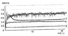
表1は、3つの市販プロダクト(A,B,C)について測定された硬さ、摩耗深さ及び摩擦係数を、及び本発明によるコーティング(D)について測定された同じ特性を表す。POD摩耗試験を、300rpmのスピードにおける200gの酸化アルミニウムボールにより行った。新規なコーティングの摩耗試験においてAl2O3ボールは摩耗したが、コーティングの方は無傷のままであった。 Table 1 represents the hardness, wear depth and coefficient of friction measured for three commercial products (A, B, C) and the same properties measured for the coating (D) according to the invention. The POD wear test was performed with 200 g aluminum oxide balls at a speed of 300 rpm. In the new coating wear test, the Al 2 O 3 balls were worn, but the coating remained intact.

新規なコーティングDの摩擦係数と参照コーティングA,B及びCの摩擦係数との違いは、図11にも説明される。 The difference between the coefficient of friction of the new coating D and that of the reference coatings A, B and C is also illustrated in FIG.
試験の結果は、第1の加熱ステップの温度が200℃から700℃に上昇するにつれ、コーティングの硬さが増大することを示す。プロ背志賀、1の加熱ステップのみを有するならば、400℃乃至600℃の温度は、硬さ値1600乃至1900HVを与える。対照的に、先行技術のプロセスを使用する場合、最大達成可能硬さ値は約1800HVである。 The results of the test show that the hardness of the coating increases as the temperature of the first heating step increases from 200 ° C to 700 ° C. A temperature of 400 ° C. to 600 ° C. gives a hardness value of 1600 to 1900 HV if it has only one heating step. In contrast, when using prior art processes, the maximum achievable hardness value is about 1800 HV.
第2の加熱ステップは、第1の加熱ステップで得られた硬さをさらに増大することが発見された。2000HVを優に超える硬さ値が測定でき、当該硬さ値は2500乃至3000HVと高い。第2の加熱処理の持続時間は、最大硬さを達成するため、第1の熱処理において使用された温度に基づき最適化されるべきであることもまた発見された。 It has been discovered that the second heating step further increases the hardness obtained in the first heating step. A hardness value well above 2000 HV can be measured, and the hardness value is as high as 2500 to 3000 HV. It has also been discovered that the duration of the second heat treatment should be optimized based on the temperature used in the first heat treatment to achieve maximum hardness.
複合熱処理の最適組み合わせは、実験的に求められ得た。 The optimum combination of complex heat treatments could be determined experimentally.
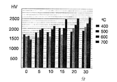
図1は、複合熱処理の第2のステップの長さと温度の関数として、新規なコーティングの硬さ値を表す。第1のステップは、400℃で45分間続いた。第2のステップは、400℃,500℃,600℃及び700℃の温度で実施した。各温度において処理は、5,10,15,20もしくは30分間続いた。硬さ値を、グラフにおいて0分と示される第1のステップの後にも測定した。 FIG. 1 represents the hardness value of the new coating as a function of the length and temperature of the second step of the composite heat treatment. The first step lasted 45 minutes at 400 ° C. The second step was performed at temperatures of 400 ° C, 500 ° C, 600 ° C and 700 ° C. Treatment at each temperature lasted 5, 10, 15, 20 or 30 minutes. The hardness value was also measured after the first step shown as 0 minutes in the graph.
400℃における第1のステップと700℃における第2のステップとの組み合わせにより、良い結果が達成できた。硬さ値約2500HVが、700℃及び持続時間15乃至30分で実施された第2のステップの後で測定された。 Good results were achieved by a combination of the first step at 400 ° C. and the second step at 700 ° C. A hardness value of about 2500 HV was measured after the second step carried out at 700 ° C. and duration 15-30 minutes.
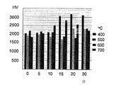
図2は、同様な方法で新規なコーティングの硬さ値を表す。この場合において、第1のステップは、700℃で30分間続いた。第2のステップは、400℃,500℃,600℃及び700℃の温度で実施した。各温度において処理は、5,10,15,20もしくは30分間続いた。硬さ値を、グラフにおいて0分と示される第1のステップの後にも測定した。 FIG. 2 represents the hardness value of the new coating in a similar manner. In this case, the first step lasted 30 minutes at 700 ° C. The second step was performed at temperatures of 400 ° C, 500 ° C, 600 ° C and 700 ° C. Treatment at each temperature lasted 5, 10, 15, 20 or 30 minutes. The hardness value was also measured after the first step shown as 0 minutes in the graph.
700℃における第1のステップと400℃における第2のステップとの組み合わせにより、良い結果が達成できた。硬さ値約3000HVが、400℃及び持続時間15乃至30分で実施された第2のステップの後で測定された。 Good results were achieved by a combination of the first step at 700 ° C. and the second step at 400 ° C. A hardness value of about 3000 HV was measured after the second step carried out at 400 ° C. and duration 15-30 minutes.
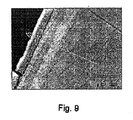
図9は、被覆表面の断面のSEM顕微鏡写真を表す。本発明によるコーティングから取られた断面図は、コーティング内に3又は4の異なる層の存在を確認した。被覆金属基質の熱処理は、Ni−P含有層及びCr含有層に影響し、拡散の結果、コーティング層内で及びコーティング層どうしで様々な相を作り出し、当該相は、例えば機械的活動に対するメッキのパフォーマンスを改善する。ハイパー3元多相(multiphase)合金は、熱処理の際に生成した新規な極めて硬質な構造を含有する。 FIG. 9 represents a SEM micrograph of a cross section of the coated surface. The cross-section taken from the coating according to the invention confirmed the presence of 3 or 4 different layers within the coating. The heat treatment of the coated metal substrate affects the Ni-P-containing layer and the Cr-containing layer, and as a result of diffusion, creates various phases within the coating layer and between the coating layers, which phase is, for example, plated for mechanical activity. Improve performance. Hyper ternary multiphase alloys contain a new and extremely hard structure produced during heat treatment.
Crの薄層(好ましくは10μm)、及び好適な複合熱処理シーケンスにより、低い摩擦係数と非常に高い硬さを有するメッキされた金属表面が製造され得ることが確認できた。 It has been confirmed that a thin layer of Cr (preferably 10 μm) and a suitable combined heat treatment sequence can produce a plated metal surface with a low coefficient of friction and a very high hardness.
実施例2
鋼基質を、厚さ7μmを有するNi−Pの相と厚さ4μmを有するCrの相とで被覆した。熱処理を2ステップで実施した: 第1のステップは400℃で45分間続き、第2のステップは700℃で30分間続いた。
Example 2
The steel substrate was coated with a Ni-P phase having a thickness of 7 μm and a Cr phase having a thickness of 4 μm. The heat treatment was carried out in two steps: the first step lasted 45 minutes at 400 ° C. and the second step lasted 30 minutes at 700 ° C.
複合熱処理後のコーティングについて測定された硬さ値は、10gの負荷で測定された約2500HVであった。 The hardness value measured for the coating after the composite heat treatment was about 2500 HV measured at a load of 10 g.
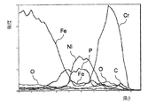
層状構造が、被覆表面の断面顕微鏡写真において認められた。コーティングの組成は、電子ビームにサンプル画像の上のラインを追わせること、及びその空間勾配に沿って以前に同定された元素の相対的な割合のプロットを生成することにより、エネルギー分散型X線分光計(EDS)により分析した。図3は、サンプルのEDSスペクトルを表す。左側に、鋼基質がある。右側に、コーティングの外側表面がある。 A layered structure was observed in the cross-sectional micrograph of the coated surface. The composition of the coating is determined by letting the electron beam follow the line above the sample image, and by generating a plot of the relative proportion of previously identified elements along its spatial gradient, Analysis was performed by a spectrometer (EDS). FIG. 3 represents the EDS spectrum of the sample. On the left is a steel substrate. On the right side is the outer surface of the coating.
サンプル内に以下の層(鋼基質からコーティングの外側表面に向かって進む)が認められる:
−Feリッチな層(鋼基質),
−主としてFe及びNiを含有する層,
−主としてNi及びPを含有する層,
−主としてNi及びCrを含有する層,
−主としてCr及びOを含有する層,
−主としてCr及びCを含有する層。
The following layers are observed in the sample (going from the steel substrate towards the outer surface of the coating):
-Fe rich layer (steel substrate),
A layer mainly containing Fe and Ni,
A layer mainly containing Ni and P,
A layer mainly containing Ni and Cr,
A layer mainly containing Cr and O,
A layer mainly containing Cr and C;
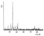
サンプルのX線回折スペクトル(XRD)をも測定した。図4は、サンプルのXRDスペクトルの一部を表す。 The X-ray diffraction spectrum (XRD) of the sample was also measured. FIG. 4 represents a portion of the XRD spectrum of the sample.
実施例3
別の鋼基質を、実施例2に置けると同様なコーティング: 厚さ7μmを有するニッケルリンの層及び厚さ4μmを有するクロムの層で被覆した。熱処理は、2ステップを2ステップで実施した: 第1のステップは400℃で30分間続き、第2のステップは700℃で30分間続いた。
Example 3
Another steel substrate was coated with the same coating as in Example 2: a layer of nickel phosphorus having a thickness of 7 μm and a layer of chromium having a thickness of 4 μm. The heat treatment was carried out in two steps in two steps: the first step lasted 30 minutes at 400 ° C. and the second step lasted 30 minutes at 700 ° C.
被覆され且つ熱処理された金属基質について測定された硬さ値は、10gの負荷で測定された約2500乃至3000HVであった。 The hardness value measured for the coated and heat treated metal substrate was about 2500 to 3000 HV measured at a load of 10 g.
層状構造が、コーティングの断面顕微鏡写真において認められた。図5は、サンプルのEDSスペクトルを表す。サンプル内に以下の層(鋼基質からコーティングの外側表面に向かって進む)が認められる:
−Feリッチな層(鋼基質),
−主としてFe及びNiを含有する層,
−主としてNi及びPを含有する層,
−主としてNi及びCrを含有する層,
−主としてCr及びOを含有する層,
−主としてCr及びCを含有する層。
A layered structure was observed in the cross-sectional micrograph of the coating. FIG. 5 represents the EDS spectrum of the sample. The following layers are observed in the sample (going from the steel substrate towards the outer surface of the coating):
-Fe rich layer (steel substrate),
A layer mainly containing Fe and Ni,
A layer mainly containing Ni and P,
A layer mainly containing Ni and Cr,
A layer mainly containing Cr and O,
A layer mainly containing Cr and C;
図6は、サンプルのXRDスペクトルの一部を表す。 FIG. 6 represents a portion of the XRD spectrum of the sample.
図4(400℃+700℃)及び図6(700℃+400℃)のXRDスペクトルは、いずれの場合において、コーティング内に存在する結晶性の相があることを意味する。比較のため、図10は、ニッケルと3価クロムで被覆され、熱処理された鋼基質を有する現在の技術水準の参照サンプルのXRDスペクトルを表す。このサンプルの硬さは、1800HVである。図4及び図4のスペクトルは、図10のスペクトルと異なることは明らかである。 The XRD spectra of FIG. 4 (400 ° C. + 700 ° C.) and FIG. 6 (700 ° C. + 400 ° C.) mean that in each case there is a crystalline phase present in the coating. For comparison, FIG. 10 represents an XRD spectrum of a current state of the art reference sample having a steel substrate coated with nickel and trivalent chromium and heat treated. The hardness of this sample is 1800 HV. Obviously, the spectra of FIGS. 4 and 4 are different from the spectra of FIG.
実施例4
被覆表面の相構造の表面近くの深さプロファイルを得るのに、すれすれの入射(grazing incidence)回折(GID)を使用した。結果を図7に示す(底部に慣用のXRDスペクトルを有する)。入射角度1.2°,5.5°及び8.5°は、コーティングの異なる深さを表す。異なる入射角で測定されたXRDスペクトルのピークは、測定されたスペクトルと、被覆基質内に含まれることが知られた元素のスペクトルとを比較することにより同定された。
Example 4
Grazing incidence diffraction (GID) was used to obtain a near-surface depth profile of the phase structure of the coated surface. The results are shown in FIG. 7 (having a conventional XRD spectrum at the bottom). The incident angles of 1.2 °, 5.5 ° and 8.5 ° represent different depths of the coating. The peaks of the XRD spectrum measured at different angles of incidence were identified by comparing the measured spectrum with the spectra of elements known to be contained within the coated substrate.
被覆表面のXRDスペクトルは、2つの高いピークと複数の低いピークとを含有する。第1のピークは、Ni3P,Ni及びCrの結晶性相に対応する44乃至45°の回折角度2θ近くに位置する。コーティング内に結晶性isovite(Cr,Fe)23C6,CrNi及びCr2Bの痕跡も存在する。第2のピークは、Ni及びCrNiの結晶性相に対応する51乃至52°の回折角度2θ近くに位置する。加えて、表面近くの層内に、Cr2O3,Cr3C2,Cr2B及びCrFeOの結晶性相のエビデンスが存在する。コーティング内深くに、Ni3P,Ni,Cr,FeNi,Cr2O3及びCrNiの結晶性相のエビデンスが存在する。ED測定(エネルギー分散型X線分光計,実施例2参照)において、CrNiの存在も検出できた。 The XRD spectrum of the coated surface contains two high peaks and multiple low peaks. The first peak is located near the diffraction angle 2θ of 44 to 45 ° corresponding to the crystalline phases of Ni 3 P, Ni and Cr. There are also traces of crystalline isovite (Cr, Fe) 23 C 6 , CrNi and Cr 2 B in the coating. The second peak is located near the diffraction angle 2θ of 51 to 52 ° corresponding to the crystalline phases of Ni and CrNi. In addition, there is evidence of crystalline phases of Cr 2 O 3 , Cr 3 C 2 , Cr 2 B and CrFeO in the layer near the surface. Deep within the coating is evidence of crystalline phases of Ni 3 P, Ni, Cr, FeNi, Cr 2 O 3 and CrNi. In the ED measurement (energy dispersive X-ray spectrometer, see Example 2), the presence of CrNi could also be detected.
実施例5
硬化可能なもしくは表面硬化された金属物体を、1μmのストライクニッケル、3μmのNi−P層及び4μmのCr層で被覆した。コーティングの合計厚さは、約8μmであった。これの後、物体を誘導加熱により熱処理した。
Example 5
A curable or surface hardened metal object was coated with 1 μm strike nickel, 3 μm Ni-P layer and 4 μm Cr layer. The total thickness of the coating was about 8 μm. After this, the object was heat treated by induction heating.
まず、出力26kW及びスピード1500mm/minを有する誘導ループにより、物体を予備加熱した。次いで、物体表面の温度を、出力26kW及びスピード1500mm/minを有する誘導により850℃まで上昇させた。その後、物体を水噴射により冷却した。 First, the object was preheated by an induction loop having an output of 26 kW and a speed of 1500 mm / min. The temperature of the object surface was then raised to 850 ° C. by induction with an output of 26 kW and a speed of 1500 mm / min. Thereafter, the object was cooled by water jet.
基材の表面を、約1mmの深さ及び増大したコーティングの硬さまで硬化させた。硬化後の基材のロックウェル硬さは58HRCであり、コーティングのビッカースマイクロ硬さは約1800HVであった。 The surface of the substrate was cured to a depth of about 1 mm and increased coating hardness. The hardened substrate Rockwell hardness was 58 HRC and the coating Vickers micro hardness was about 1800 HV.
実施例6
硬化可能な金属物体を、1μmのストライクニッケル層、3μmのNi−P層及び4μmのCr層で被覆した。コーティングの合計厚さは、約8μmであった。これの後、物体を、1ステップの誘導加熱により熱処理した。
Example 6
A curable metal object was coated with a 1 μm strike nickel layer, a 3 μm Ni—P layer and a 4 μm Cr layer. The total thickness of the coating was about 8 μm. After this, the object was heat treated by one-step induction heating.
物体表面の温度を、出力60kW及びスピード1500mm/minを有する誘導により850℃まで上昇させた。その後、物体を水噴射により冷却した。 The temperature of the object surface was raised to 850 ° C. by induction with an output of 60 kW and a speed of 1500 mm / min. Thereafter, the object was cooled by water jet.
基材を硬化させ、コーティングの硬さは増大した。硬化後の基材のロックウェル硬さは55HRCであり、コーティングのビッカースマイクロ硬さは約1600HVであった。 The substrate was cured and the hardness of the coating increased. The hardened substrate Rockwell hardness was 55 HRC and the coating Vickers micro hardness was about 1600 HV.
実施例7
物体を、7μmのNi−P層及び5μmのCr層で被覆した。被覆物体を700℃で30分間加熱した。この後、ダイヤモンドライクカーボン(DLC)のトップ層を、薄膜堆積により、被覆物体の上に堆積させた。
Example 7
The object was covered with a 7 μm Ni-P layer and a 5 μm Cr layer. The coated object was heated at 700 ° C. for 30 minutes. After this, a diamond-like carbon (DLC) top layer was deposited on the coated object by thin film deposition.
コーティングは非常に硬質であった。被覆表面のピンオンディスク滑り摩耗は、0μmであった(試験条件: 210分、500g負荷及び300rpm)。被覆表面の摩擦係数は0.24であった。AASS腐食試験は、200hを超える値を与えた。 The coating was very hard. The pin-on-disk sliding wear on the coated surface was 0 μm (test conditions: 210 minutes, 500 g load and 300 rpm). The coefficient of friction of the coated surface was 0.24. The AASS corrosion test gave a value in excess of 200 h.
あるいはまた、トップ層を、Ni−P,Crコーティングの上に直接適用した。この場合において、熱処理は、薄膜堆積ステップの後に実施できた。 Alternatively, the top layer was applied directly over the Ni-P, Cr coating. In this case, the heat treatment could be performed after the thin film deposition step.
技術の進歩と共に、本発明の基本理念を様々なやり方で実施されてよいことは、当業者にとって明らかである。従って本発明とその実施形態は、上記の実施例に限定されるのではなく、請求項の範囲内において異なり得る。 It will be apparent to those skilled in the art that with the advancement of technology, the basic idea of the present invention may be implemented in various ways. Accordingly, the invention and its embodiments are not limited to the examples described above but may vary within the scope of the claims.
Claims (20)
―金属基質上にニッケルリン合金の層を堆積させるステップと;
−前記Ni−Pの層上に3価クロム浴由来のクロム層を電解メッキするステップと;
−コーティングを硬化させるため、及び結晶性Niと結晶性Ni3Pとを含有する少なくとも1の層及び結晶性Crと結晶性CrNiとを含有する少なくとも1の層を包含する多相層を生成するため、被覆金属基質に1以上の熱処理を施すステップと
を有する、方法。 A method for producing a trivalent chromium-based coating on a metal substrate comprising the following steps:
-Depositing a layer of nickel phosphorus alloy on the metal substrate;
Electroplating a chromium layer derived from a trivalent chromium bath on the Ni-P layer;
Producing a multiphase layer for curing the coating and including at least one layer containing crystalline Ni and crystalline Ni 3 P and at least one layer containing crystalline Cr and crystalline CrNi Subjecting the coated metal substrate to one or more heat treatments.
―金属基質上に光沢Niの層を堆積させるステップと;
−前記光沢Niの層の上にNi−Pの層を堆積させるステップと;
−前記Ni−Pの層の上に3価のクロムの層を電解メッキするステップと;
−被覆金属基質に200乃至500℃で15乃至30分間熱処理を施すステップと
を有する、方法。 The method of claim 1 for producing a decorative and corrosion resistant coating on a metal substrate, comprising the following steps:
Depositing a layer of bright Ni on the metal substrate;
Depositing a layer of Ni-P on the layer of bright Ni;
Electroplating a layer of trivalent chromium on the Ni-P layer;
Subjecting the coated metal substrate to a heat treatment at 200 to 500 ° C. for 15 to 30 minutes.
−金属基質上にNi−Pの層を堆積させるステップと;
―Ni−Pの層の上に3価のクロムの層を電解メッキするステップと;
―前記被覆金属基質に650乃至750℃で15乃至30分間第1の熱処理を施すステップと;
―前記被覆金属基質に400乃至500℃で15乃至30分間第2の熱処理を施すステップと
を有する、方法。 A method according to claim 1 for producing a hard chrome coating on a metal substrate, comprising the following steps:
Depositing a layer of Ni-P on the metal substrate;
Electroplating a layer of trivalent chromium on the layer of Ni-P;
-Subjecting the coated metal substrate to a first heat treatment at 650-750 ° C for 15-30 minutes;
-Subjecting the coated metal substrate to a second heat treatment at 400-500 ° C for 15-30 minutes.
ニッケルリン合金の層を堆積させるステップと、Ni−Pの層上に3価クロム浴由来のクロム層を電解メッキするステップとを少なくとも1回繰り返すステップを有し、その後被覆金属基質は、前記1以上の熱処理を施される、方法。 A method according to claim 1 for producing a multilayer coating on a metal substrate, comprising:
The step of depositing a layer of nickel phosphorus alloy and the step of electrolytically plating a chromium layer derived from a trivalent chromium bath on the layer of Ni-P is repeated at least once, after which the coated metal substrate comprises the aforementioned 1 A method in which the above heat treatment is performed.
Applications Claiming Priority (3)
| Application Number | Priority Date | Filing Date | Title |
|---|---|---|---|
| PCT/FI2013/050038 WO2014111616A1 (en) | 2013-01-15 | 2013-01-15 | Method for producing a chromium coating on a metal substrate |
| FIPCT/FI2013/050038 | 2013-01-15 | ||
| PCT/FI2014/050029 WO2014111624A1 (en) | 2013-01-15 | 2014-01-15 | Method for producing a chromium coating on a metal substrate |
Publications (2)
| Publication Number | Publication Date |
|---|---|
| JP2016509128A true JP2016509128A (en) | 2016-03-24 |
| JP6576832B2 JP6576832B2 (en) | 2019-09-18 |
Family
ID=51209056
Family Applications (1)
| Application Number | Title | Priority Date | Filing Date |
|---|---|---|---|
| JP2015552117A Active JP6576832B2 (en) | 2013-01-15 | 2014-01-15 | Method for producing a chromium coating on a metal substrate and coated article |
Country Status (8)
| Country | Link |
|---|---|
| US (1) | US20150361571A1 (en) |
| EP (1) | EP2946031A4 (en) |
| JP (1) | JP6576832B2 (en) |
| CN (1) | CN104995339B (en) |
| BR (1) | BR112015016656B1 (en) |
| CA (1) | CA2897265C (en) |
| EA (1) | EA030470B1 (en) |
| WO (2) | WO2014111616A1 (en) |
Cited By (1)
| Publication number | Priority date | Publication date | Assignee | Title |
|---|---|---|---|---|
| JP2017508879A (en) * | 2014-01-15 | 2017-03-30 | サヴロック リミテッド | Method for producing chromium coating and coated object |
Families Citing this family (15)
| Publication number | Priority date | Publication date | Assignee | Title |
|---|---|---|---|---|
| US10443142B2 (en) | 2014-01-15 | 2019-10-15 | Savroc Ltd | Method for producing chromium-containing multilayer coating and a coated object |
| EP3167100B1 (en) * | 2014-07-11 | 2020-02-26 | Savroc Ltd | A chromium-containing coating and a coated object |
| DE102015202910A1 (en) | 2015-02-18 | 2016-08-18 | Dr.-Ing. Max Schlötter GmbH & Co KG | Tin-nickel layer with high hardness |
| DE102015208644A1 (en) * | 2015-05-11 | 2016-11-17 | Schaeffler Technologies AG & Co. KG | Component, use of the component and method for producing the component |
| WO2017042420A1 (en) | 2015-09-09 | 2017-03-16 | Savroc Ltd | Chromium-based coating, a method for producing a chromium-based coating and a coated object |
| DE102016004913A1 (en) * | 2016-04-22 | 2017-10-26 | Grohe Ag | Method for coating an article by means of a multilayer system with a nickel-phosphorus alloy |
| JP6417438B2 (en) * | 2017-03-22 | 2018-11-07 | 株式会社リケン | Composite chrome plating film and piston ring having the film |
| CN106906496A (en) * | 2017-03-24 | 2017-06-30 | 武汉迪赛环保新材料股份有限公司 | A kind of method for preparing trivalent chromium plating coating in steel surface |
| CN106929892A (en) * | 2017-04-10 | 2017-07-07 | 武汉迪赛新材料有限公司 | A kind of preparation method of high corrosion-resistant high rigidity Trivalent hard chromium coating |
| US11149851B2 (en) | 2018-09-13 | 2021-10-19 | Tenneco Inc. | Piston ring with wear resistant coating |
| FI129420B (en) | 2020-04-23 | 2022-02-15 | Savroc Ltd | An aqueous electroplating bath |
| CN111705345B (en) * | 2020-06-04 | 2021-12-21 | 东华大学 | Composite preparation process of coating suitable for grooved needle |
| CN113652690B (en) * | 2021-07-27 | 2023-07-21 | 平顶山平煤机煤矿机械装备有限公司 | Metal surface treatment method for electroless nickel-phosphorus alloy sleeve plating of hard chromium |
| EP4357487A1 (en) | 2022-10-18 | 2024-04-24 | Centre de Recherches Métallurgiques ASBL - Centrum voor Research in de Metallurgie VZW | Work roll coating and method for producing the same |
| CN117364079B (en) * | 2023-12-04 | 2024-03-29 | 江西联创电子有限公司 | High-temperature performance toughening method of die and die |
Citations (7)
| Publication number | Priority date | Publication date | Assignee | Title |
|---|---|---|---|---|
| JPS54124831A (en) * | 1978-03-22 | 1979-09-28 | Mishima Kosan Co Ltd | Production of casting mold for continuous casting |
| JPS6013094A (en) * | 1983-06-30 | 1985-01-23 | Seiko Instr & Electronics Ltd | Production of band for wristwatch |
| JPS63203792A (en) * | 1987-02-17 | 1988-08-23 | Kobe Steel Ltd | Production of mold for continuous casting |
| US5252360A (en) * | 1990-03-15 | 1993-10-12 | Huettl Wolfgang | Process for the protection of an engraved roll or plate by coating an engraved surface with an interlayer and thereafter applying a wear-resistant layer to the interlayer by PVD |
| JPH06248472A (en) * | 1993-02-22 | 1994-09-06 | Kawasaki Heavy Ind Ltd | Corrosion resistant and wear resistant multilayer metal film and its formation |
| JPH0995793A (en) * | 1995-09-29 | 1997-04-08 | Shigeo Hoshino | Tervalent chromium plating bath depositing chromium plating having thermally hardening property |
| JP2002285375A (en) * | 2001-03-28 | 2002-10-03 | Chunichi Craft Kk | Trivalent chromium plating bath |
Family Cites Families (14)
| Publication number | Priority date | Publication date | Assignee | Title |
|---|---|---|---|---|
| US3164897A (en) | 1958-03-27 | 1965-01-12 | Patriarca Peter | Method of brazing |
| US4461680A (en) * | 1983-12-30 | 1984-07-24 | The United States Of America As Represented By The Secretary Of Commerce | Process and bath for electroplating nickel-chromium alloys |
| JPS60196209A (en) * | 1984-03-19 | 1985-10-04 | Sumitomo Metal Ind Ltd | Three-layer plated hot rolling roll |
| DE4008254A1 (en) * | 1990-03-15 | 1991-09-19 | Huettl & Vester Gmbh | METHOD FOR PRODUCING ENGRAVED ROLLS OR PLATES |
| US5413646A (en) * | 1991-02-08 | 1995-05-09 | Blount, Inc. | Heat-treatable chromium |
| US5271823A (en) | 1992-06-17 | 1993-12-21 | Eaton Corporation | Method of making a trivalent chromium plated engine valve |
| KR100503497B1 (en) | 2002-11-25 | 2005-07-26 | 한국기계연구원 | Heat treating method for improving the wear-resistance and corrosion-resistance of chromium platings |
| JP4571546B2 (en) * | 2005-07-13 | 2010-10-27 | 株式会社神戸製鋼所 | Wear resistant parts and power transmission parts |
| WO2008057123A1 (en) | 2006-11-09 | 2008-05-15 | Massachusetts Institute Of Technology | Preparation and properties of cr-c-p hard coatings annealed at high temperature for high temperature applications |
| JP5448616B2 (en) * | 2009-07-14 | 2014-03-19 | 古河電気工業株式会社 | Copper foil with resistance layer, method for producing the copper foil, and laminated substrate |
| JP2013091811A (en) * | 2010-02-23 | 2013-05-16 | Taiyo Kagaku Kogyo Kk | Multilayer film laminate using aluminum or aluminum alloy as substrate and lamination method therefor |
| JP5563849B2 (en) * | 2010-03-02 | 2014-07-30 | 福田金属箔粉工業株式会社 | Treated copper foil |
| JP5581805B2 (en) * | 2010-05-24 | 2014-09-03 | トヨタ自動車株式会社 | Method for plating stainless steel material and plating material thereof |
| CN102644067A (en) * | 2012-03-28 | 2012-08-22 | 广州鸿葳科技股份有限公司 | Method for chemically plating double-layer Ni-P plating layer |
-
2013
- 2013-01-15 WO PCT/FI2013/050038 patent/WO2014111616A1/en active Application Filing
-
2014
- 2014-01-15 CA CA2897265A patent/CA2897265C/en active Active
- 2014-01-15 EA EA201591297A patent/EA030470B1/en unknown
- 2014-01-15 EP EP14741009.6A patent/EP2946031A4/en active Pending
- 2014-01-15 WO PCT/FI2014/050029 patent/WO2014111624A1/en active Application Filing
- 2014-01-15 CN CN201480004867.2A patent/CN104995339B/en active Active
- 2014-01-15 JP JP2015552117A patent/JP6576832B2/en active Active
- 2014-01-15 BR BR112015016656-3A patent/BR112015016656B1/en active IP Right Grant
- 2014-01-15 US US14/761,179 patent/US20150361571A1/en not_active Abandoned
Patent Citations (7)
| Publication number | Priority date | Publication date | Assignee | Title |
|---|---|---|---|---|
| JPS54124831A (en) * | 1978-03-22 | 1979-09-28 | Mishima Kosan Co Ltd | Production of casting mold for continuous casting |
| JPS6013094A (en) * | 1983-06-30 | 1985-01-23 | Seiko Instr & Electronics Ltd | Production of band for wristwatch |
| JPS63203792A (en) * | 1987-02-17 | 1988-08-23 | Kobe Steel Ltd | Production of mold for continuous casting |
| US5252360A (en) * | 1990-03-15 | 1993-10-12 | Huettl Wolfgang | Process for the protection of an engraved roll or plate by coating an engraved surface with an interlayer and thereafter applying a wear-resistant layer to the interlayer by PVD |
| JPH06248472A (en) * | 1993-02-22 | 1994-09-06 | Kawasaki Heavy Ind Ltd | Corrosion resistant and wear resistant multilayer metal film and its formation |
| JPH0995793A (en) * | 1995-09-29 | 1997-04-08 | Shigeo Hoshino | Tervalent chromium plating bath depositing chromium plating having thermally hardening property |
| JP2002285375A (en) * | 2001-03-28 | 2002-10-03 | Chunichi Craft Kk | Trivalent chromium plating bath |
Cited By (1)
| Publication number | Priority date | Publication date | Assignee | Title |
|---|---|---|---|---|
| JP2017508879A (en) * | 2014-01-15 | 2017-03-30 | サヴロック リミテッド | Method for producing chromium coating and coated object |
Also Published As
| Publication number | Publication date |
|---|---|
| BR112015016656B1 (en) | 2021-09-28 |
| EA030470B1 (en) | 2018-08-31 |
| CN104995339B (en) | 2021-02-12 |
| BR112015016656A2 (en) | 2017-07-11 |
| CA2897265C (en) | 2021-02-16 |
| JP6576832B2 (en) | 2019-09-18 |
| CN104995339A (en) | 2015-10-21 |
| EA201591297A1 (en) | 2016-01-29 |
| CA2897265A1 (en) | 2014-07-24 |
| US20150361571A1 (en) | 2015-12-17 |
| WO2014111624A1 (en) | 2014-07-24 |
| WO2014111616A1 (en) | 2014-07-24 |
| EP2946031A1 (en) | 2015-11-25 |
| EP2946031A4 (en) | 2016-10-26 |
Similar Documents
| Publication | Publication Date | Title |
|---|---|---|
| JP6576832B2 (en) | Method for producing a chromium coating on a metal substrate and coated article | |
| JP6774135B2 (en) | How to make a chrome coating and the coated object | |
| US10443142B2 (en) | Method for producing chromium-containing multilayer coating and a coated object | |
| EP3167100B1 (en) | A chromium-containing coating and a coated object | |
| EP3350359B1 (en) | Chromium-based coating, a method for producing a chromium-based coating and a coated object | |
| JP4762077B2 (en) | Hardening method of steel member, hardened steel member and hardened surface protective agent | |
| JP5258928B2 (en) | Hardening method of steel member, hardened steel member and hardened surface protective agent |
Legal Events
| Date | Code | Title | Description |
|---|---|---|---|
| A621 | Written request for application examination |
Free format text: JAPANESE INTERMEDIATE CODE: A621 Effective date: 20170106 |
|
| A977 | Report on retrieval |
Free format text: JAPANESE INTERMEDIATE CODE: A971007 Effective date: 20180216 |
|
| A131 | Notification of reasons for refusal |
Free format text: JAPANESE INTERMEDIATE CODE: A131 Effective date: 20180313 |
|
| A521 | Request for written amendment filed |
Free format text: JAPANESE INTERMEDIATE CODE: A523 Effective date: 20180611 |
|
| A131 | Notification of reasons for refusal |
Free format text: JAPANESE INTERMEDIATE CODE: A131 Effective date: 20181113 |
|
| A521 | Request for written amendment filed |
Free format text: JAPANESE INTERMEDIATE CODE: A523 Effective date: 20190212 |
|
| TRDD | Decision of grant or rejection written | ||
| A01 | Written decision to grant a patent or to grant a registration (utility model) |
Free format text: JAPANESE INTERMEDIATE CODE: A01 Effective date: 20190723 |
|
| A61 | First payment of annual fees (during grant procedure) |
Free format text: JAPANESE INTERMEDIATE CODE: A61 Effective date: 20190821 |
|
| R150 | Certificate of patent or registration of utility model |
Ref document number: 6576832 Country of ref document: JP Free format text: JAPANESE INTERMEDIATE CODE: R150 |
|
| R250 | Receipt of annual fees |
Free format text: JAPANESE INTERMEDIATE CODE: R250 |
|
| R250 | Receipt of annual fees |
Free format text: JAPANESE INTERMEDIATE CODE: R250 |