JP2016224198A - Image display device - Google Patents

Image display device Download PDF

Info

Publication number
JP2016224198A
JP2016224198A JP2015109227A JP2015109227A JP2016224198A JP 2016224198 A JP2016224198 A JP 2016224198A JP 2015109227 A JP2015109227 A JP 2015109227A JP 2015109227 A JP2015109227 A JP 2015109227A JP 2016224198 A JP2016224198 A JP 2016224198A
Authority
JP
Japan
Prior art keywords
light
guide plate
liquid crystal
light emitting
light guide
Prior art date
Legal status (The legal status is an assumption and is not a legal conclusion. Google has not performed a legal analysis and makes no representation as to the accuracy of the status listed.)
Pending
Application number
JP2015109227A
Other languages
Japanese (ja)
Other versions
JP2016224198A5 (en
Inventor
市原 高明
Takaaki Ichihara
高明 市原
後藤 聡
Satoshi Goto
聡 後藤
鉦一郎 江口
Shoichiro Eguchi
鉦一郎 江口
Current Assignee (The listed assignees may be inaccurate. Google has not performed a legal analysis and makes no representation or warranty as to the accuracy of the list.)
Daiichi Shokai Co Ltd
Original Assignee
Daiichi Shokai Co Ltd
Priority date (The priority date is an assumption and is not a legal conclusion. Google has not performed a legal analysis and makes no representation as to the accuracy of the date listed.)
Filing date
Publication date
Application filed by Daiichi Shokai Co Ltd filed Critical Daiichi Shokai Co Ltd
Priority to JP2015109227A priority Critical patent/JP2016224198A/en
Publication of JP2016224198A publication Critical patent/JP2016224198A/en
Publication of JP2016224198A5 publication Critical patent/JP2016224198A5/ja
Pending legal-status Critical Current

Links

Images

Landscapes

  • Liquid Crystal Display Device Control (AREA)
  • Control Of Indicators Other Than Cathode Ray Tubes (AREA)
  • Liquid Crystal (AREA)
  • Planar Illumination Modules (AREA)

Abstract

PROBLEM TO BE SOLVED: To provide an image display device displaying images with diversity.SOLUTION: The image display device includes a transmissive liquid crystal panel 550e capable of displaying an image by using a surface light-emitting plate as a backlight. The surface light-emitting plate includes a first light source (light guide upper decorative substrate 550d1) that radiates light in a first direction (from an upper part) on a side of a light guide plate 550d and a second light source (light guide plate left decorative substrate 550d5) that radiates light in a second direction on the side of the light guide plate. The light guide plate includes a first light emission region 550d4 that emits light when irradiated with light from the first light source and a second light emission region 550d5 that emits light when irradiated with light from the second light source. When light emission modes by the first light source and the second light source are switched from one to the other by light emission switching means, images partially visible on a part of the display panel are switched.SELECTED DRAWING: Figure 5

Description

本発明は、画像の表示を行う画像表示装置に関する。   The present invention relates to an image display device that displays an image.

画像を表示する画像表示装置として、面発光源をバックライトとして画像表示可能な液晶表示パネルとを備えた液晶表示装置が知られている(特許文献1参照)。   As an image display device for displaying an image, a liquid crystal display device including a liquid crystal display panel capable of displaying an image using a surface light source as a backlight is known (see Patent Document 1).

特開2007−264183号公報JP 2007-264183 A

特許文献1に記載されるような従来の画像表示装置は、面発光源で表示パネル全体をムラなく明るく照明することで、表示パネル全体に画像を表示するものであった。そのため、画像の表示の見せ方の観点からすると、多様性に乏しかった。   The conventional image display device as described in Patent Document 1 displays an image on the entire display panel by illuminating the entire display panel brightly and uniformly with a surface emitting source. For this reason, from the viewpoint of how to display an image, the diversity was poor.

そこで、本発明は、このような事情を鑑みてなされたものであり、その目的は、多様性のある画像表示を行う画像表示装置を提供することにある。   Therefore, the present invention has been made in view of such circumstances, and an object thereof is to provide an image display apparatus that performs various image displays.

請求項1に係る画像表示装置は、
面発光板と、前記面発光板に光を入射可能な光源と、
前記面発光板をバックライトとして、画像表示可能な透過型の表示パネルと、
を備えたものであって、上記課題を解決するために、
前記光源は、前記面発光板の側部の第1の方向から光を照射する第1の光源と、前記面発光板の側部の第2の方向から光を照射する第2の光源とを少なくとも備え、
前記第1の光源と前記第2の光源の発光を切り替える発光切替手段を備え、
前記面発光板は、
前記第1の光源から光を照射したときに発光する第1の発光領域と、
前記第2の光源から光を照射したときに発光する第2の発光領域とを備えた、
ことを特徴とする。
An image display apparatus according to claim 1 is provided.
A surface light emitting plate, and a light source capable of making light incident on the surface light emitting plate,
Using the surface-emitting plate as a backlight, a transmissive display panel capable of displaying an image,
In order to solve the above problems,
The light source includes: a first light source that emits light from a first direction of a side portion of the surface light emitting plate; and a second light source that emits light from a second direction of the side portion of the surface light emitting plate. At least,
A light emission switching means for switching light emission of the first light source and the second light source;
The surface emitting plate is
A first light emitting region that emits light when irradiated with light from the first light source;
A second light emitting region that emits light when irradiated with light from the second light source,
It is characterized by that.

請求項1に係る画像表示装置によれば、画像表示可能な透過型の表示パネルのバックライトとしての面発光板の第1の光源を発光させて、面発光板の側部の第1の方向から光を照射すると、面発光板の第1の発光領域が発光し、表示パネルでは第1の発光領域に対応する部分の画像が視認される。また、面発光板の第2の光源を発光させて、面発光板の側部の第2の方向から光を照射すると、面発光板の第2の発光領域が発光し、表示パネルでは第2の発光領域に対応する部分の画像が視認される。第1の光源と第2の光源の発光を切り替える発光切替手段を備えているため、表示パネルで視認される画像が切り替えられることになる。表示パネルが透過型であるため、第1の発光領域を発光させている場合には、第1の発光領域以外の領域に対応する表示パネルの部分が、第2の発光領域を発光させている場合には、第2の発光領域以外の領域に対応する表示パネルの部分が、発光領域に比べて表示パネルの後方に存在する物が容易に視認される。そのため、今までにない新鮮味のある画像表示を行うことができる。   According to the image display device of the first aspect, the first light source of the surface light emitting plate as the backlight of the transmissive display panel capable of displaying an image is caused to emit light, and the first direction of the side portion of the surface light emitting plate. When the light is emitted from the first light emitting region, the first light emitting region of the surface light emitting plate emits light, and an image of a portion corresponding to the first light emitting region is visually recognized on the display panel. In addition, when the second light source of the surface light emitting plate is caused to emit light and light is irradiated from the second direction of the side portion of the surface light emitting plate, the second light emitting region of the surface light emitting plate emits light, and the display panel has the second light emission. The image of the part corresponding to the light emitting area is visually recognized. Since the light emission switching means for switching the light emission of the first light source and the second light source is provided, the image visually recognized on the display panel is switched. Since the display panel is of a transmissive type, when the first light emitting region emits light, the portion of the display panel corresponding to the region other than the first light emitting region emits the second light emitting region. In some cases, the part of the display panel corresponding to the area other than the second light emitting area is easily visually recognized in the rear of the display panel as compared with the light emitting area. Therefore, it is possible to display an image with a freshness that has never been seen before.

また、面発光板の第1の発光領域、第2の発光領域に対応する表示パネルに表示される部分的画像の形態が変わったり、視認される表示領域の形状や大きさを変えることができ、部分的画像自体の中味(見える箇所)を変化させて見せることができる。そのため、今までにない多様性のある画像表示を行うことができる。   In addition, the form of the partial image displayed on the display panel corresponding to the first light emitting area and the second light emitting area of the surface light emitting plate can be changed, and the shape and size of the visible display area can be changed. , The contents of the partial image itself can be changed. For this reason, it is possible to perform image display with unprecedented diversity.

また、面発光板の発光領域を切り替えるだけで、表示パネルに表示される画像の表示形態を変化させることができる。そのため、表示パネルの画像データをそのまま変更しなくても表示される画像の表示態様を変化させることができ、画像表示のための制御が複雑なものにならずに済む。   Moreover, the display form of the image displayed on the display panel can be changed only by switching the light emitting area of the surface light emitting plate. Therefore, the display mode of the displayed image can be changed without changing the image data of the display panel as it is, and the control for displaying the image does not have to be complicated.

液晶表示モジュールの基本構成を示す模式的断面図である。It is typical sectional drawing which shows the basic composition of a liquid crystal display module. 液晶表示モジュールにおける液晶表示パネルの構成を示す部分拡大図である。It is the elements on larger scale which show the structure of the liquid crystal display panel in a liquid crystal display module. 液晶表示モジュールにおける照明装置の構成を示す図である。It is a figure which shows the structure of the illuminating device in a liquid crystal display module. 導光板ユニットの外観の一例を示す斜視図である。It is a perspective view which shows an example of the external appearance of a light-guide plate unit. 図4に示す導光板ユニットを前面から見た場合の構成例を示す前面分解斜視図である。It is a front exploded perspective view which shows the structural example at the time of seeing the light-guide plate unit shown in FIG. 4 from the front. 図4に示す導光板ユニットを後面から見た場合の外観の一例を示す斜視図である。It is a perspective view which shows an example of the external appearance at the time of seeing the light-guide plate unit shown in FIG. 4 from the rear surface. 図4に示す導光板ユニットを後面から見た場合の構成例を示す後面分解斜視図である。It is a rear surface exploded perspective view which shows the structural example at the time of seeing the light-guide plate unit shown in FIG. 4 from the rear surface. 導光板ユニットの断面構成の一例を示す断面図である。It is sectional drawing which shows an example of the cross-sectional structure of a light-guide plate unit. 画像表示装置の電気系統を示す要部ブロック図である。It is a principal part block diagram which shows the electric system of an image display apparatus. 画像表示装置における導光板を発光させたときに視認される液晶パネルの表示状態を示しており、(A)導光板の第1の発光領域のみを面発光した場合を示す正面図、(B)導光板の第2の発光領域のみを面発光した場合を示す正面図、(C)導光板の第1の発光領域と第2の発光領域とを一緒に面発光した場合を示す正面図である。The display state of the liquid crystal panel visually recognized when light is emitted from the light guide plate in the image display device is shown. (A) Front view showing a case where only the first light emitting region of the light guide plate is surface-emitted, (B) It is a front view which shows the case where only the 2nd light emission area | region of a light-guide plate carries out surface emission, (C) The front view which shows the case where the 1st light emission area | region of a light guide plate and a 2nd light emission area | region are surface-emitted together. .

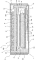
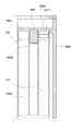
以下、本発明の実施例を図面に基づいて詳細に説明する。まず、液晶表示モジュールの基本構成について説明する。図1は液晶表示モジュールの基本構成を示す模式的断面図であり、図2は液晶表示モジュールにおける液晶表示パネルの構成を示す部分拡大図である。また、図3は液晶表示モジュールにおける照明装置の構成を示す図である。   Hereinafter, embodiments of the present invention will be described in detail with reference to the drawings. First, the basic configuration of the liquid crystal display module will be described. FIG. 1 is a schematic sectional view showing a basic configuration of a liquid crystal display module, and FIG. 2 is a partially enlarged view showing a configuration of a liquid crystal display panel in the liquid crystal display module. FIG. 3 is a diagram showing a configuration of an illumination device in the liquid crystal display module.

図1に示されるように、本液晶表示モジュールの筐体は、扁平な直方体をなす箱の天板を除去した形状の収納ケース1に、底板を除去した同形状のカバーケース2が、嵌装されてなる。これら両ケース1、2は、共に金属板を加工して形成されている。カバーケース2の天板201には、表示を観察するための表示窓202が穿設されている。   As shown in FIG. 1, the housing of the present liquid crystal display module includes a storage case 1 having a shape obtained by removing a top plate of a flat rectangular parallelepiped box, and a cover case 2 having the same shape from which a bottom plate has been removed. Being done. Both of these cases 1 and 2 are formed by processing a metal plate. A display window 202 for observing the display is formed in the top plate 201 of the cover case 2.

上記筐体内には、フレーム3が配置されている。本実施形態のフレーム3は、共に空間外形が扁平な直方体をなす前室3aと後室3bとが2段に重設されてなる。すなわち、直方体の空間を囲む枠体をなす側板301の所定高さ位置に、その内面全周にわたって仕切り棚302が突設され、この仕切り棚302を境界として、前室3aと後室3bとが2段に重設され、これら前室3aと後室3bは、仕切り棚302で囲まれた空間により連通されている。   A frame 3 is disposed in the casing. The frame 3 according to the present embodiment includes a front chamber 3a and a rear chamber 3b, which are formed in a rectangular parallelepiped with a flat space outer shape, in two stages. That is, a partition shelf 302 protrudes over the entire inner surface of the side plate 301 that forms a frame surrounding the rectangular space, and the front chamber 3a and the rear chamber 3b are separated from each other by using the partition shelf 302 as a boundary. The front chamber 3 a and the rear chamber 3 b are connected in two stages, and are communicated with each other by a space surrounded by the partition shelf 302.

フレーム3の前室3aには、液晶表示パネル4が収納されている。本実施形態の液晶表示パネル4は、アクティブマトリクス方式の液晶表示パネルであり、平面外形が矩形をなす液晶セル5を挟んで表示の観察側となる前側に、同様の矩形をなす前位相差板6と前偏光板7がそれぞれ順次配置され、その後側に、同じく矩形をなす後位相差板8と後偏光板9がそれぞれ順次配置されてなる。   A liquid crystal display panel 4 is accommodated in the front chamber 3 a of the frame 3. The liquid crystal display panel 4 of the present embodiment is an active matrix type liquid crystal display panel, and a front retardation plate having a similar rectangular shape on the front side, which is a viewing side of display, with a liquid crystal cell 5 having a rectangular planar outer shape interposed therebetween. 6 and the front polarizing plate 7 are sequentially arranged, and a rear retardation plate 8 and a rear polarizing plate 9 having the same rectangular shape are sequentially arranged on the rear side.

液晶セル5では、図2に示されるように、一対の前ガラス基板51、後ガラス基板52が、枠状シール材(不図示)により所定の間隙を保ち接合され、これら前、後ガラス基板51、52間の枠状シール材で囲まれた空間内には液晶が封入されて液晶層53が形成されている。   In the liquid crystal cell 5, as shown in FIG. 2, a pair of front glass substrate 51 and rear glass substrate 52 are joined together with a predetermined gap by a frame-shaped sealing material (not shown). , 52 encloses a frame-shaped sealing material between which liquid crystal is sealed to form a liquid crystal layer 53.

接合された一対の前、後ガラス基板51、52のうちの一方の前ガラス基板51の対向面(内面)には、画素を画定するためのブラックマスク54が設置されている。ブラックマスク54には、形成すべき画素に対応させて複数の開口がマトリックス配置で形成されている。   On the opposing surface (inner surface) of one front glass substrate 51 of the pair of front and rear glass substrates 51, 52, a black mask 54 for defining pixels is provided. In the black mask 54, a plurality of openings are formed in a matrix arrangement corresponding to the pixels to be formed.

ブラックマスク54の各開口には、赤、緑、青の3種類のカラーフィルタ55R、55G、55Bが所定の配置でそれぞれ設置され、カラーフィルタ層55が形成されている。ここで、各カラーフィルタ55R、55G、55Bは、各開口よりも全周にわたり適長幅だけ大きい面積を備えており、周縁部をブラックマスク54の開口縁部に重畳させて設置されている。   In each opening of the black mask 54, three kinds of color filters 55R, 55G, and 55B of red, green, and blue are respectively installed in a predetermined arrangement, and a color filter layer 55 is formed. Here, each of the color filters 55R, 55G, and 55B has an area that is larger than the respective openings by an appropriate length over the entire circumference, and the peripheral edge portion is disposed so as to overlap the opening edge portion of the black mask 54.

赤、緑、青の各色カラーフィルタ55R、55G、55Bからなるカラーフィルタ層55には、各色カラーフィルタ55R、55G、55Bを一括して覆う一枚膜状の透明導電膜からなる共通電極56が被着されている。そして、共通電極56の表面には、液晶分子の配向を規制する前水平配向膜57が一様に被着されている。   The color filter layer 55 composed of the color filters 55R, 55G, and 55B for red, green, and blue has a common electrode 56 that is composed of a single transparent film that covers the color filters 55R, 55G, and 55B collectively. It is attached. A front horizontal alignment film 57 that regulates the alignment of liquid crystal molecules is uniformly deposited on the surface of the common electrode 56.

一方、後ガラス基板52の内面には、前述した各ブラックマスク54の開口に対応させて、透明導電膜からなる複数の画素電極58が同様にマトリックス配置で設置されている。各画素電極58には、スイッチング用能動素子としての薄膜トランジスタ59が、それぞれ設置接続されている。なお、各薄膜トランジスタ59を介して画素電極58を作動させるためのゲート、ドレイン、及びソースの各配線や各配線間の絶縁膜等の図示は省略されている。そして、全ての画素電極58及び薄膜トランジスタ59等を覆って後水平配向膜61が一様に被着されている。   On the other hand, on the inner surface of the rear glass substrate 52, a plurality of pixel electrodes 58 made of a transparent conductive film are similarly arranged in a matrix arrangement so as to correspond to the openings of the respective black masks 54 described above. A thin film transistor 59 serving as an active element for switching is installed and connected to each pixel electrode 58. The gate, drain, and source wirings for operating the pixel electrode 58 through the thin film transistors 59, and an insulating film between the wirings are not shown. A rear horizontal alignment film 61 is uniformly deposited so as to cover all the pixel electrodes 58 and the thin film transistors 59 and the like.

上述のように配向処理された前、後水平配向膜57、61によって挟持された液晶層53の各液晶分子60は、電界が印加されていない初期状態においては、両水平配向膜57、61それぞれに施された配向処理方向57a、61aに沿った配向規制力を受けている。   The liquid crystal molecules 60 of the liquid crystal layer 53 sandwiched by the rear horizontal alignment films 57 and 61 before and after the alignment treatment as described above are respectively in the horizontal alignment films 57 and 61 in an initial state where no electric field is applied. Is subjected to the alignment regulating force along the alignment processing directions 57a and 61a.

図1に戻って、本例の液晶セル5における一対のガラス基板51、52の大きさは、表示面側となる前ガラス基板51よりも後ガラス基板52の方が大きく、これら大きさの異なるガラス基板51、52は後ガラス基板52の一縁辺が前ガラス基板51の対応する縁辺から突出する配置で接合されている。後ガラス基板52の突出縁辺52aには、各電極から引き出された配線とその各端部の接続端子(不図示)が配設されて駆動回路部が形成されており、この駆動回路部には駆動回路素子としてのドライバLSI11がCOG(Chip On Glass)搭載されている。そして、この駆動回路部の先端縁に設けられている入力端子列には、フレキシブル配線基板(FPC:Flexible Printed Circuit)12が導通接合されている。   Returning to FIG. 1, the size of the pair of glass substrates 51 and 52 in the liquid crystal cell 5 of this example is larger in the rear glass substrate 52 than in the front glass substrate 51 on the display surface side, and these sizes are different. The glass substrates 51 and 52 are joined in an arrangement in which one edge of the rear glass substrate 52 protrudes from a corresponding edge of the front glass substrate 51. On the projecting edge 52a of the rear glass substrate 52, wirings led out from the respective electrodes and connection terminals (not shown) at respective ends thereof are arranged to form a driving circuit unit. A driver LSI 11 as a drive circuit element is mounted on COG (Chip On Glass). A flexible printed circuit (FPC) 12 is conductively joined to the input terminal row provided at the leading edge of the drive circuit section.

フレーム3の後室3b内には、サイドライト型の面状照明装置13が収容されている。本実施形態のサイドライト型の面状照明装置13は、照射対象の液晶表示パネル4に大略対応した矩形をなす透明な導光板14の一端面141に、点光源としての発光ダイオード(以下、LED(Light−Emitting Diode)という)15がその光射出面を密接させて設置され、導光板14の液晶表示パネル4に対向させる前面142とは反対側の後面143には光反射シート16が設置されて、構成されている。導光板14の光反射シート16が設置された後面143には、LED15から射出され一端面141から導光板14内に入射した光を前面142に向けて反射させるための同心円状の凹凸パターン(不図示)が形成されている。   A sidelight type planar illumination device 13 is accommodated in the rear chamber 3 b of the frame 3. The sidelight type planar illumination device 13 of the present embodiment has a light emitting diode (hereinafter referred to as an LED) as a point light source on one end surface 141 of a transparent light guide plate 14 having a rectangular shape substantially corresponding to the liquid crystal display panel 4 to be irradiated. (Light-Emitting Diode) 15 is installed with its light emitting surface closely attached, and a light reflecting sheet 16 is installed on the rear surface 143 of the light guide plate 14 opposite to the front surface 142 facing the liquid crystal display panel 4. Configured. On the rear surface 143 of the light guide plate 14 on which the light reflecting sheet 16 is installed, a concentric concave / convex pattern (non-uniform) for reflecting the light emitted from the LEDs 15 and entering the light guide plate 14 from the one end surface 141 toward the front surface 142. (Shown) is formed.

本実施形態では図3に示されるように2個のLED15、15が配置されており、これらLED15、15は、各光射出面を導光板14の一端面141に密接させた状態で、フレキシブル配線基板17上にCOF(Chip On Film)方式により直接搭載されている。   In this embodiment, two LEDs 15 and 15 are arranged as shown in FIG. 3, and these LEDs 15 and 15 are flexible wirings in a state where each light emitting surface is in close contact with one end surface 141 of the light guide plate 14. It is directly mounted on the substrate 17 by a COF (Chip On Film) method.

各LED15は、それぞれ、図3に示されるように、赤、緑、青の各波長光を射出する赤、緑、青の各色LEDチップ15r、15g、15bからなり、各色LEDチップ15r、15g、15bから射出される赤、緑、青の各波長光が混色された白色光が出射される三波長型白色点光源である。各色LEDチップ15r、15g、15bから射出される赤、緑、青の各波長光の強度は、各LEDチップ13r、13g、13bの駆動電流を制御することにより調整される。   As shown in FIG. 3, each LED 15 includes red, green, and blue color LED chips 15r, 15g, and 15b that emit light of red, green, and blue wavelengths, and each color LED chip 15r, 15g, This is a three-wavelength white point light source that emits white light in which red, green, and blue wavelength lights emitted from 15b are mixed. The intensity of each wavelength light of red, green, and blue emitted from each color LED chip 15r, 15g, 15b is adjusted by controlling the drive current of each LED chip 13r, 13g, 13b.

図1に示されるように、導光板14の前面142には、光拡散シート18とプリズムシート19が、その順序で重畳設置されている。光拡散シート18は導光板14から面状に出射される照射光の輝度分布を均一化するために、プリズムシート19は照射光の出射方向を正面方向に揃えるために、それぞれ設置されている。   As shown in FIG. 1, a light diffusion sheet 18 and a prism sheet 19 are superimposed on the front surface 142 of the light guide plate 14 in that order. The light diffusion sheet 18 is installed in order to make the luminance distribution of the irradiation light emitted from the light guide plate 14 planar, and the prism sheet 19 is installed to align the emission direction of the irradiation light in the front direction.

そして、上述のように構成された面状照明装置13は、後室3b内の所定位置に、背面パネル21に支持された状態で収納されている。背面パネル21は、フレーム後室3bの底面を閉じる配置で、フレーム3に嵌合装着されている。   And the planar illuminating device 13 comprised as mentioned above is accommodated in the state supported by the back panel 21 in the predetermined position in the back chamber 3b. The rear panel 21 is fitted and attached to the frame 3 so as to close the bottom surface of the frame rear chamber 3b.

背面パネル21の後面側で収納ケース1における底板101の内面には、駆動制御回路基板22が設置されている。この駆動制御回路基板22は、本液晶表示モジュール全体の駆動を制御するものであり、液晶表示パネル4の駆動制御回路やLED15の駆動制御回路が設けられている。したがって、この駆動制御回路基板22には、前述した液晶表示パネル4の後ガラス基板52の突出縁辺52aの先端部に導通接合され、LED15がCOF搭載されているフレキシブル配線基板17が半田接合により導通接続されているフレキシブル配線基板12が、コネクタ23を介して電気接続されている。   A drive control circuit board 22 is installed on the inner surface of the bottom plate 101 in the storage case 1 on the rear surface side of the rear panel 21. The drive control circuit board 22 controls the drive of the entire liquid crystal display module, and is provided with a drive control circuit for the liquid crystal display panel 4 and a drive control circuit for the LEDs 15. Accordingly, the drive control circuit board 22 is conductively bonded to the tip of the protruding edge 52a of the rear glass substrate 52 of the liquid crystal display panel 4 described above, and the flexible wiring board 17 on which the LED 15 is mounted by COF is conductively connected by solder bonding. The connected flexible wiring board 12 is electrically connected via the connector 23.

ここで、LED15の駆動制御回路は、図3に示されるように、各LED15を定電流駆動するLEDドライバ回路221と、制御演算部222及びメモリ223からなる。このメモリ223に書き込まれたデータに基づき、各色LEDチップ15r、15g、15bを駆動すべき電流値が制御演算部222により演算され、各LEDチップ15r、15g、15bがLEDドライバ回路221を介して駆動制御される。   Here, as shown in FIG. 3, the drive control circuit of the LED 15 includes an LED driver circuit 221 that drives each LED 15 at a constant current, a control calculation unit 222, and a memory 223. Based on the data written in the memory 223, the current value for driving the LED chips 15r, 15g, and 15b is calculated by the control calculation unit 222, and the LED chips 15r, 15g, and 15b are connected via the LED driver circuit 221. Drive controlled.

以上に説明した液晶表示モジュールは、バックライトとしての導光板14が側部の一方向のみから光を照射されて導光板のほほ全域が発光するものであった。   In the liquid crystal display module described above, the light guide plate 14 as a backlight is irradiated with light from only one side of the side portion, so that almost the entire light guide plate emits light.

[画像表示装置550]
以下に説明する画像表示装置550は、導光板(面発光板に相当する)と、導光板に光を入射可能な光源と、面発光源をバックライトとして画像表示可能な透過型の表示パネルを有し、光源が、導光板の側部の第1の方向から光を照射する第1の光源と、導光板の側部の第2の方向から光を照射する第2の光源とを少なくとも備え、導光板が、第1の光源から光を照射したときに発光する第1の発光領域と、第2の光源から光を照射したときに発光する第2の発光領域とを備えているものである。また、第1の光源と第2の光源の発光を切り替える発光切替手段を備える。そうして、導光板の一部を部分的に面発光することで、表示パネルの一部を部分的に見せるものである。
[Image display device 550]
An image display device 550 described below includes a light guide plate (corresponding to a surface light-emitting plate), a light source capable of entering light into the light guide plate, and a transmissive display panel capable of displaying an image using the surface light-emitting source as a backlight. And a light source includes at least a first light source that emits light from a first direction of a side portion of the light guide plate and a second light source that emits light from a second direction of the side portion of the light guide plate. The light guide plate includes a first light emitting region that emits light when irradiated with light from the first light source, and a second light emitting region that emits light when irradiated with light from the second light source. is there. Also provided is a light emission switching means for switching light emission of the first light source and the second light source. Thus, a part of the display panel is partially shown by partially emitting a part of the light guide plate.

以下、本実施例の画像表示装置550について、主として図4乃至図9を参照して詳細に説明する。ます、図4は画像表示装置の外観の一例を示す斜視図であり、図5は図4に示す画像表示装置を前面から見た場合の構成例を示す前面分解斜視図である。また、図6は図4に示す導光板ユニットを後面から見た場合の外観の一例を示す斜視図であり、図7は図4に示す導光板ユニットを後面から見た場合の構成例を示す後面分解斜視図である。さらに、図8は画像表示装置の断面構成の一例を示す断面図である。また、図9は画像表示装置の電気系統を示す要部ブロック図である。   Hereinafter, the image display device 550 of the present embodiment will be described in detail mainly with reference to FIGS. 4 to 9. FIG. 4 is a perspective view showing an example of the appearance of the image display device, and FIG. 5 is a front exploded perspective view showing a configuration example when the image display device shown in FIG. 4 is viewed from the front. 6 is a perspective view showing an example of the appearance when the light guide plate unit shown in FIG. 4 is viewed from the rear surface, and FIG. 7 shows a configuration example when the light guide plate unit shown in FIG. 4 is viewed from the rear surface. It is a rear surface exploded perspective view. Further, FIG. 8 is a cross-sectional view showing an example of a cross-sectional configuration of the image display device. FIG. 9 is a principal block diagram showing an electrical system of the image display apparatus.

画像表示装置550は、図4乃至図7に示すように全体として平板状の箱部材である。画像表示装置550は、図4の前面斜視図に示すように正面に表示領域となるべき開口部が形成された平板形状のフレーム550cに、図6の後面斜視図に示すように透明な裏蓋550lが着脱可能に取り付けられている。フレーム550cは、その上端面及び下端面は平坦な面で構成されている一方、その両側面には突起部が形成されている。   The image display device 550 is a flat plate member as a whole as shown in FIGS. 4 to 7. As shown in the front perspective view of FIG. 4, the image display device 550 has a flat frame 550c in which an opening to be a display area is formed in the front, and a transparent back cover as shown in the rear perspective view of FIG. 550 l is detachably attached. The frame 550c has a flat upper end surface and a lower end surface, and protrusions are formed on both side surfaces thereof.

この画像表示装置550を分解すると、図5の前面分解斜視図及び図7の後面分解斜視図に示すようにフレーム550cと裏蓋550lとの間に、液晶パネル550e、スペーサ550s及び導光板550dがほぼ平行となるように配列している。なお、詳細は後述するが、導光板550dは、例えば、上面及び左側面などの端面から入射された光をその内部で反射させて拡散することにより、その表面から均一な光を出射するパネルの一種である。   When the image display device 550 is disassembled, a liquid crystal panel 550e, a spacer 550s, and a light guide plate 550d are provided between the frame 550c and the back cover 550l as shown in the front exploded perspective view of FIG. 5 and the rear exploded perspective view of FIG. They are arranged so that they are almost parallel. Although details will be described later, the light guide plate 550d is, for example, a panel that emits uniform light from its surface by reflecting and diffusing light incident from the end surfaces such as the upper surface and the left side surface. It is a kind.

液晶パネル550eは、図5及び図7に示すように透明な矩形の平板状部材であり、その上端面及び下端面に各々2つの取付部550e1,550e2によってフレーム550c内に固定されている。液晶パネル550eは、その矩形の平板状部材の表面に沿って薄く広がる矩形の液晶部550e3、及び、その矩形の周囲を包囲する形状の透明パネル550e4を備えている。   The liquid crystal panel 550e is a transparent rectangular flat plate member as shown in FIGS. 5 and 7, and is fixed in the frame 550c by two attachment portions 550e1 and 550e2 on the upper end surface and the lower end surface, respectively. The liquid crystal panel 550e includes a rectangular liquid crystal portion 550e3 that spreads thinly along the surface of the rectangular flat plate member, and a transparent panel 550e4 that surrounds the rectangle.

液晶部550e3は、基本的な構成は図2において説明したように、互いの偏光方向を所定の角度(例えば直角)とした2枚の偏光層を備えていると共に、これら2枚の偏光層の間に、多数の液晶分子が配列された液晶層を備えている。なお、配向膜などその他の構成については説明を省略する。液晶部550eは、例えば、図9に示す表示制御基板473による通電状態の制御に応じて、上記多数の液晶分子の配列状態を制御することにより光の透過量が制御される。この液晶部550e3は、例えば、三原色に相当する透明な複数のドット毎に設けられた一対の透明電極への通電状態に応じてそれら各部分における各液晶分子の配列が変わり、それら複数のドット毎に、一方の偏光層を通過した光が他方の偏光層を通過する光量を調整することができる。   As described in FIG. 2, the liquid crystal unit 550e3 includes two polarizing layers whose polarization directions are set to a predetermined angle (for example, a right angle). A liquid crystal layer in which a large number of liquid crystal molecules are arranged is provided therebetween. Note that description of other components such as an alignment film is omitted. The liquid crystal unit 550e controls the light transmission amount by controlling the alignment state of the liquid crystal molecules in accordance with, for example, control of the energization state by the display control board 473 shown in FIG. In the liquid crystal unit 550e3, for example, the arrangement of the liquid crystal molecules in each part changes according to the energization state to a pair of transparent electrodes provided for each of a plurality of transparent dots corresponding to the three primary colors. In addition, the amount of light that passes through one polarizing layer can be adjusted.

導光板550dは、矩形の平板状の透明パネルであって、その透明パネルの上端面に導光板上装飾基板550d1(第1の光源)が設けられていると共に、その透明パネルの左側端面に導光板左装飾基板550d2(第2の光源)が設けられている。   The light guide plate 550d is a rectangular flat transparent panel. A light guide plate decoration substrate 550d1 (first light source) is provided on the upper end surface of the transparent panel, and the light guide plate 550d is guided to the left end surface of the transparent panel. An optical plate left decorative substrate 550d2 (second light source) is provided.

本実施例では、導光板550dの側部の第1の方向から光を照射する一例として、導光板550dの上端面の上方から光を照射するものとしている。また、導光板550dの側部の第2の方向から光を照射する一例として、導光板550dの左側端面の左方から光を照射するものとしている。これらは、第1の方向及び第2の方向の一例であって、例えば、第1の方向を下方とし、第2の方向を右方としてもよい。   In the present embodiment, as an example of irradiating light from the first direction of the side portion of the light guide plate 550d, light is irradiated from above the upper end surface of the light guide plate 550d. In addition, as an example of irradiating light from the second direction of the side portion of the light guide plate 550d, light is irradiated from the left side of the left end surface of the light guide plate 550d. These are examples of the first direction and the second direction. For example, the first direction may be the lower side and the second direction may be the right side.

導光板550dは、導光板上装飾基板550d1の光源の点灯により、導光板550dの上端面から内部に光が入射された際に、正面から見た場合、例えば、左右方向における当該平板状の透明パネルの中央部よりも右側に偏った領域に面発光源としての発光領域550d4が形成されるように、その透明パネルの裏面(背面)における発光領域550d4(第1の発光領域に相当する)に多数の反射部が加工形成されている。本例では、発光領域550d4は、円形状とされている。   When the light guide plate 550d is viewed from the front when light is incident from the upper end surface of the light guide plate 550d by turning on the light source of the decorative substrate 550d1 on the light guide plate, the light guide plate 550d is, for example, the flat transparent plate in the left-right direction. A light emitting region 550d4 (corresponding to the first light emitting region) on the back surface (back surface) of the transparent panel is formed so that a light emitting region 550d4 as a surface light source is formed in a region that is biased to the right side of the center of the panel. A large number of reflective portions are formed by machining. In this example, the light emitting region 550d4 has a circular shape.

また、導光板550dは、導光板左装飾基板550d2の光源の点灯により、導光板550dの左側端面から内部に光が入射された際に、正面から見た場合、例えば、左右方向における当該平板状の透明パネルの中央部の領域に面発光源としての発光領域550d5が形成されるように、その透明パネルの裏面(背面)における発光領域550d5(第2の発光領域に相当する)に多数の反射部が加工形成されている。本例では、発光領域550d5は、三角形状とされている。   In addition, the light guide plate 550d is, for example, the flat plate in the left-right direction when viewed from the front when light is incident from the left end surface of the light guide plate 550d by turning on the light source of the light guide plate left decorative substrate 550d2. A large number of reflections on the light emitting region 550d5 (corresponding to the second light emitting region) on the back surface (back surface) of the transparent panel so that a light emitting region 550d5 as a surface light source is formed in the central region of the transparent panel. The part is processed and formed. In this example, the light emitting region 550d5 has a triangular shape.

また、導光板550dでは、平板状の透明パネルの発光領域500d4及び発光領域d5以外の領域は、反射部が形成されていないため、上記光源を点灯しても発光しない非発光領域550d3とされている。   In addition, in the light guide plate 550d, areas other than the light emitting area 500d4 and the light emitting area d5 of the flat transparent panel are not formed with a reflecting portion, and thus are non-light emitting areas 550d3 that do not emit light even when the light source is turned on. Yes.

導光板550dにおいては、導光板上装飾基板550d1から出力された光(第1の光源からの光)がその上端面から入射されて透明パネルの内部を進みながら、上述のように透明パネルの裏面(背面)に形成した発光領域550d4の多数の反射部において反射し、主として正面から円形状となって出力される。なお、この場合、発光領域550d5の反射部は、上方から進んで来た光に対しては正面方向に向けて発光しないように形成されている。   In the light guide plate 550d, the light (light from the first light source) output from the light guide plate upper decorative substrate 550d1 enters from the upper end surface and travels through the transparent panel, as described above. The light is reflected at a large number of reflecting portions of the light emitting region 550d4 formed on the (rear surface), and is output in a circular shape mainly from the front. In this case, the reflecting portion of the light emitting region 550d5 is formed so as not to emit light in the front direction with respect to light traveling from above.

一方、導光板左装飾基板550d2から出力された光(第2の光源からの光)がその左側端面から入射されて透明パネルの内部を進みながら、上述のように透明パネルの裏面(背面)に形成した発光領域550d5の多数の反射部において反射し、主として正面から三角形状となって出力される。なお、この場合、右方の発光領域550d4の反射部は、左方から進んで来た光に対しては正面方向に向けて発光しないように形成されている。   On the other hand, light (light from the second light source) output from the light guide plate left decorative substrate 550d2 is incident from the left end surface thereof and travels through the transparent panel, as described above, on the back surface (back surface) of the transparent panel as described above. The light is reflected at a large number of reflecting portions of the formed light emitting region 550d5, and is output in a triangular shape mainly from the front. In this case, the reflecting portion of the right light emitting region 550d4 is formed so as not to emit light in the front direction with respect to light traveling from the left.

即ち、導光板550dは、導光板上装飾基板550d1から光を照射した場合には、上述のように左右方向の右側において円形状をなした発光領域550d4から正面方向(フレーム550cの方向)に面発光するのである。これにより、液晶パネル550eには、導光板550dの右側で面発光された円形状の光が入射されることになり、正面から見た場合、液晶パネル550eの制御態様に応じて液晶パネル550eの右側において円形状の内側部分に絵柄(画像)を容易に視認することができるようになる。   That is, the light guide plate 550d faces the front direction (the direction of the frame 550c) from the light emitting region 550d4 having a circular shape on the right side in the left-right direction as described above when irradiated with light from the decorative substrate 550d1 on the light guide plate. It emits light. Thereby, the circular light surface-emitted on the right side of the light guide plate 550d is incident on the liquid crystal panel 550e. When viewed from the front, the liquid crystal panel 550e is controlled according to the control mode of the liquid crystal panel 550e. On the right side, the pattern (image) can be easily visually recognized in the circular inner portion.

また、導光板550dは、導光板左装飾基板550d2から光を照射した場合には、上述のように左右方向の中央部において三角形状をなした発光領域550d5から正面方向(フレーム550cの方向)に面発光するのである。これにより、液晶パネル550eには、導光板550dの中央部で面発光された三角形状の光が入射されることになり、正面から見た場合、液晶パネル550eの制御態様に応じて液晶パネル550eの中央部において三角形状の内側部分に絵柄(画像)を容易に視認することができるようになる。   In addition, when light is emitted from the light guide plate left decorative substrate 550d2, the light guide plate 550d extends in the front direction (the direction of the frame 550c) from the light emitting region 550d5 having a triangular shape at the center in the left-right direction as described above. It emits surface light. As a result, the triangular light surface-emitted at the center of the light guide plate 550d is incident on the liquid crystal panel 550e. When viewed from the front, the liquid crystal panel 550e is controlled according to the control mode of the liquid crystal panel 550e. The pattern (image) can be easily visually recognized on the inner part of the triangle shape at the center of the image.

以上のように、例えば、導光板550dは、発光領域550d4及び/または発光領域550d5を面発光させるかに応じて、画像表示装置550の液晶パネル500eにおいて視認される画像の場所を左右方向において移動させることができる。また、見える画像の場所が変わる毎に液晶パネル500eにおいて視認されるその画像内容も変化するのである。また、発光領域550d4及び発光領域550d5のうちの何れかを面発光させるかによって、液晶パネル550eにて画像を視認できる表示領域の形状や大きさを変えることができる。そのため、今までにない多様性のある画像表示を行うことができる。   As described above, for example, the light guide plate 550d moves in the left-right direction the location of the image that is visually recognized on the liquid crystal panel 500e of the image display device 550, depending on whether the light-emitting area 550d4 and / or the light-emitting area 550d5 emits light. Can be made. Further, every time the location of the visible image changes, the image content visually recognized on the liquid crystal panel 500e also changes. In addition, the shape and size of the display area where an image can be visually recognized on the liquid crystal panel 550e can be changed depending on which of the light emitting area 550d4 and the light emitting area 550d5 is surface-emitting. For this reason, it is possible to perform image display with unprecedented diversity.

さらに詳しく画像表示装置550の構造について説明すると、画像表示装置550は、図8の部分断面斜視図に示すようにフレーム550cの前面に形成された開口部から、図示しない薄い透明パネルを介して液晶パネル550eの一部が表示領域として露出している。フレーム550cに裏蓋550lを装着することによって形成される画像表示装置550の内部には、上述のように、液晶パネル550eの表面に沿って設けられたスペーサ550s及び導光板550dが互いに平行となるように配置している。   The structure of the image display device 550 will be described in more detail. The image display device 550 has a liquid crystal display through a thin transparent panel (not shown) from an opening formed on the front surface of the frame 550c as shown in the partial sectional perspective view of FIG. A part of the panel 550e is exposed as a display area. As described above, the spacer 550s and the light guide plate 550d provided along the surface of the liquid crystal panel 550e are parallel to each other in the image display device 550 formed by attaching the back cover 550l to the frame 550c. Are arranged as follows.

画像表示装置550に内蔵されている導光板550dには、図8の部分断面図に示すように、上端面に、基材550d7に多数のLED550d6が実装された導光板上装飾基板550d1が設けられていると共に、図8においては図示を省略しているが、左側端面に、同様に基材に多数のLEDが実装された導光板左装飾基板550d2が設けられている。これら導光板上装飾基板550d1及び導光板下装飾基板550d2は、図9に示す制御基板471の制御による通電状態に応じて各LED550d6が光を出力する。これらの光は、導光板550dの内部を通して反射され、前述のように円形状の発光領域550d4及び三角形状の発光領域550d5から液晶パネル550eに向けて(上記正面方向に相当)に出力される。このように反射された光によって使用者の目には、液晶パネル550eの制御態様に応じて、この液晶パネル550eを通して、例えば絵柄として視認されるようになる。   As shown in the partial cross-sectional view of FIG. 8, the light guide plate 550d built in the image display device 550 is provided with a decorative plate 550d1 on the light guide plate in which a large number of LEDs 550d6 are mounted on a base material 550d7. In addition, although not shown in FIG. 8, a light guide plate left decorative substrate 550d2 in which a number of LEDs are similarly mounted on a base material is provided on the left end surface. The LED 550d6 outputs light to the decorative substrate 550d1 on the light guide plate and the decorative substrate 550d2 under the light guide plate according to the energized state under the control of the control substrate 471 shown in FIG. These lights are reflected through the inside of the light guide plate 550d and output from the circular light emitting region 550d4 and the triangular light emitting region 550d5 toward the liquid crystal panel 550e (corresponding to the front direction) as described above. The user's eyes are thus visually recognized through the liquid crystal panel 550e as, for example, a picture depending on the control mode of the liquid crystal panel 550e.

導光板550dは、導光板上装飾基板550d1及び導光板左下装飾基板550d2に設けられた各LED550d6が発光していない状態(通常の状態)では、使用者側から液晶パネル550eにあらわされた装飾絵柄のドットを視認し難い状態となっている。これら導光板上装飾基板550d1及び導光板左装飾基板550d2は、制御基板471(図9)によって制御されている。   The light guide plate 550d is a decorative picture displayed on the liquid crystal panel 550e from the user side when the LEDs 550d6 provided on the light guide plate upper decorative substrate 550d1 and the light guide plate lower left decorative substrate 550d2 are not emitting light (normal state). It is difficult to see the dots. The light guide plate upper decorative substrate 550d1 and the light guide plate left decorative substrate 550d2 are controlled by a control substrate 471 (FIG. 9).

また、本実施形態では、透過型の液晶パネル550eの表示領域のうち、液晶パネル550eに何も画像などの絵柄が表示されていない領域については、液晶パネル550eが透過型であり、かつ裏蓋5501も透明であるため、使用者は、この領域と対応する透過型の液晶パネル550eの後方、つまり画像表示装置550の後方に存在するものを見ることができる。   In the present embodiment, among the display areas of the transmissive liquid crystal panel 550e, the liquid crystal panel 550e is a transmissive liquid crystal panel 550e and the back cover is not displayed on the liquid crystal panel 550e. Since 5501 is also transparent, the user can see what is behind the transmissive liquid crystal panel 550e corresponding to this region, that is, behind the image display device 550.

なお、図9に示すように、電源基板475から、液晶部550e、導光板上装飾基板550d1及び導光板左装飾基板550d2、制御基板471、表示制御基板473に各作動電源が供給されるようになっている。また、表示制御基板473は制御基板471からの動作信号を受けると液晶部550eに所定の画像データをセットする。   As shown in FIG. 9, the operation power is supplied from the power supply board 475 to the liquid crystal unit 550e, the light guide plate upper decoration board 550d1, the light guide plate left decoration board 550d2, the control board 471, and the display control board 473. It has become. Further, when the display control board 473 receives an operation signal from the control board 471, the display control board 473 sets predetermined image data in the liquid crystal unit 550e.

画像表示装置550は以上のような構成であり、このような構成の画像表示装置550を用いた表示の一例について図10を用いて簡単に説明する。図10(A)に示すように、導光板550dの発光領域550d4のみを面発光した場合は、導光板550dの左右方向の右側において円形状をなした発光領域550d4から正面方向(フレーム550cの方向)に面発光する。これにより、液晶部550e3には、導光板550dの右側で面発光された円形状の光が入射されることになる。正面から見た場合、液晶部550e3の制御態様に応じて液晶パネル550eの右側において円形状の内側部分にのみ絵柄(画像)を視認することができるようになる。   The image display device 550 is configured as described above, and an example of display using the image display device 550 having such a configuration will be briefly described with reference to FIG. As shown in FIG. 10A, in the case where only the light emitting region 550d4 of the light guide plate 550d emits light, the front side direction (the direction of the frame 550c) from the light emitting region 550d4 having a circular shape on the right side of the light guide plate 550d ). As a result, circular light that is surface-emitted on the right side of the light guide plate 550d is incident on the liquid crystal portion 550e3. When viewed from the front, according to the control mode of the liquid crystal unit 550e3, the picture (image) can be visually recognized only at the circular inner portion on the right side of the liquid crystal panel 550e.

この例では、液晶部550e3の中央やや右寄りに画像データとして星形画像が表示されるようにセットされており、発光領域550d4の正面方向に対応する星形画像の一部画像(右部分画像)のみが使用者に視認されるものの、発光領域550d4以外の領域の正面方向に対応する星形画像の左部分画像の殆どが使用者に対して非視認状態とされている。なお、先述したように、発光領域550d4以外の非発光領域を通して後方の背景を視認することができる。   In this example, a star image is set to be displayed as image data slightly to the right of the liquid crystal unit 550e3, and a partial image (right partial image) of the star image corresponding to the front direction of the light emitting region 550d4. However, most of the left partial image of the star image corresponding to the front direction of the area other than the light emitting area 550d4 is not visible to the user. As described above, the back background can be visually recognized through the non-light emitting area other than the light emitting area 550d4.

このように、図10(A)以下において、画像データについては、使用者に視認される部分を実線で示し、使用者に対して非視認状態とされている部分を破線で示している。   As described above, in FIG. 10A and subsequent figures, the portion of the image data that is visually recognized by the user is indicated by a solid line, and the portion that is not visible to the user is indicated by a broken line.

図10(B)では、導光板550dの発光領域550d5のみを面発光した場合を示しており、第2の導光板550fの左右方向の中央において三角形状をなした発光領域550d5から正面方向(フレーム550cの方向)に面発光する。これにより、液晶部550e3には、第2の導光板550fの中央で面発光された三角形状の光が入射されることになる。正面から見た場合、液晶部550e3の制御態様に応じて液晶パネル550eの中央において三角形状の内側部分に絵柄(画像)を容易に視認することができるようになる。   FIG. 10B shows a case where only the light emitting region 550d5 of the light guide plate 550d is surface-emitted, and a front direction (frame) from the light emitting region 550d5 having a triangular shape at the center in the left-right direction of the second light guide plate 550f. Surface light is emitted in the direction of 550c. Thus, the triangular light that is surface-emitted at the center of the second light guide plate 550f is incident on the liquid crystal unit 550e3. When viewed from the front, according to the control mode of the liquid crystal unit 550e3, the pattern (image) can be easily visually recognized on the inner side of the triangular shape at the center of the liquid crystal panel 550e.

この例では、発光領域550f4の正面方向に対応する星形画像の一部画像(左部分の先端画像)のみが使用者に視認されるものの、発光領域550d5以外の領域の正面方向に対応する星形画像の殆どが使用者に対して非視認状態とされている。   In this example, only a part of the star image corresponding to the front direction of the light emitting area 550f4 (the left end image) is visually recognized by the user, but a star corresponding to the front direction of the area other than the light emitting area 550d5. Most of the shaped images are not visible to the user.

このように、画像表示可能な透過型の液晶パネル550eのバックライトとしての面発光源の導光板550dの第1の光源(導光板上装飾基板550d1のLED550d6)を発光させて、導光板550dの側部の第1の方向(上方)から光を照射すると、導光板の第1の発光領域(発光領域550d4)が発光し、液晶パネル550eでは第1の発光領域に対応する部分の画像が容易に視認される。また、面発光源の第2の光源(導光板左装飾基板550d2のLED550d6)を発光させて、導光板の側部の第2の方向(左方)から光を照射すると、導光板の第2の発光領域(発光領域550d5)が発光し、液晶パネル550eでは第2の発光領域に対応する部分の画像が容易に視認される。第1の光源と第2の光源の発光を切り替える発光切替手段を備えているため、液晶パネル550eで視認される画像が切り替えられることになる。そのため、今までにない新鮮味のある画像表示を行うことができる。   In this way, the first light source (LED 550d6 of the decorative substrate 550d1 on the light guide plate) of the surface light emission source as the backlight of the transmissive liquid crystal panel 550e capable of displaying an image is caused to emit light, and the light guide plate 550d When light is irradiated from the first direction (upper side) of the side portion, the first light emitting region (light emitting region 550d4) of the light guide plate emits light, and an image of a portion corresponding to the first light emitting region is easy on the liquid crystal panel 550e. Visible to. Further, when the second light source (LED 550d6 of the light guide plate left decorative substrate 550d2) is made to emit light and irradiated with light from the second direction (left side) of the side portion of the light guide plate, the second light guide plate second light source is emitted. The light emitting area (light emitting area 550d5) emits light, and an image of a portion corresponding to the second light emitting area is easily visually recognized on the liquid crystal panel 550e. Since the light emission switching means for switching the light emission of the first light source and the second light source is provided, the image visually recognized on the liquid crystal panel 550e is switched. Therefore, it is possible to display an image with a freshness that has never been seen before.

また、各導光板550dが備える各発光領域550d4〜550d5は、正面視において、互いが重複しないような異なる位置に配置されているため、発光領域550d4、発光領域550d5を1つずつ選択的に切り替えて発光させると、各発光領域550d4〜550d5に対応する液晶パネル550eに表示される部分的画像の位置が移動したり、部分的画像自体の中味(見える箇所)を変化させて見せることができる。また、発光領域550d4及び発光領域550d5のうちの何れかを面発光させるかによって、液晶パネル550eにて画像を視認できる表示領域の形状や大きさを変えることができる。そのため、今までにない多様性のある画像表示を行うことができる。   Moreover, since each light emission area | region 550d4-550d5 with which each light-guide plate 550d is provided is arrange | positioned in the different position so that it may not mutually overlap in front view, it selectively switches light emission area 550d4 and light emission area 550d5 one by one When the light is emitted, the position of the partial image displayed on the liquid crystal panel 550e corresponding to each of the light emitting areas 550d4 to 550d5 can be moved, or the contents (visible portions) of the partial image itself can be changed. In addition, the shape and size of the display area where an image can be visually recognized on the liquid crystal panel 550e can be changed depending on which of the light emitting area 550d4 and the light emitting area 550d5 is surface-emitting. For this reason, it is possible to perform image display with unprecedented diversity.

さらに、導光板550dの発光領域550d4〜550d5を一緒に発光させると、発光させた導光板の各発光領域が合わさることになり、各発光領域に対応する表示パネルに表示される部分的画像の見える部分が拡がる。   Further, when the light emitting areas 550d4 to 550d5 of the light guide plate 550d are caused to emit light together, the light emitting areas of the light guide plates that are emitted are combined, and a partial image displayed on the display panel corresponding to each light emitting area can be seen. The part expands.

図10(C)では、導光板550dの発光領域550d4と発光領域550d5とを一緒に面発光した場合を示しており、導光板550dの左右方向の右側において円形状をなした発光領域550d4と、導光板550dの左右方向の中央において三角形状をなした発光領域550d5とから正面方向(フレーム550cの方向)に向けて面発光する。これにより、液晶部550e3には、導光板550dの右側で面発光された円形状の光と、導光板550dの中央で面発光された三角形状の光とが入射されることになる。正面から見た場合、液晶部550e3の制御態様に応じて液晶パネル550eの中央及び右側において三角形状の内側部分と円形状の内側部分に絵柄(画像)を容易に視認することができるようになる。   FIG. 10C shows a case where the light emitting region 550d4 and the light emitting region 550d5 of the light guide plate 550d are surface-emitted together, and a light emitting region 550d4 having a circular shape on the right side in the left-right direction of the light guide plate 550d, Surface light is emitted from the light emitting region 550d5 having a triangular shape at the center in the left-right direction of the light guide plate 550d toward the front direction (the direction of the frame 550c). As a result, circular light surface-emitted on the right side of the light guide plate 550d and triangular light surface-emitted at the center of the light guide plate 550d are incident on the liquid crystal unit 550e3. When viewed from the front, according to the control mode of the liquid crystal unit 550e3, a pattern (image) can be easily visually recognized at the center and right side of the liquid crystal panel 550e on the triangular inner portion and the circular inner portion. .

この例では、発光領域550d5の正面方向に対応する星形画像の一部画像(中央から左側の先端部分画像)と、発光領域550d4の正面方向に対応する星形画像の一部画像(右部分画像)の両方が使用者に視認される。しかしながら、発光領域550d4及び発光領域d5以外の非発光領域の正面方向に対応する星形画像(略中央の部分画像)は使用者に対して非視認状態とされている。   In this example, a partial image of the star image corresponding to the front direction of the light emitting area 550d5 (a tip partial image on the left side from the center) and a partial image of the star image corresponding to the front direction of the light emitting area 550d4 (the right part) Both images are visible to the user. However, the star image (substantially central partial image) corresponding to the front direction of the non-light emitting areas other than the light emitting area 550d4 and the light emitting area d5 is not visible to the user.

このように、導光板550dの発光領域550d4〜550d5を選択して一緒に発光させると、発光させた導光板の各発光領域が合わさることになり、各発光領域に対応する表示パネルに表示される部分的画像の見える部分が拡がる。そのため、今までにない新鮮味と多様性のある画像表示を行うことができる。   As described above, when the light emitting areas 550d4 to 550d5 of the light guide plate 550d are selected to emit light together, the light emitting areas of the light guide plates that have been emitted are combined and displayed on the display panel corresponding to each light emitting area. The visible part of the partial image is expanded. Therefore, it is possible to display images with freshness and diversity that have never been seen before.

また、逆に、導光板の2つの発光領域を発光させた状態から1つの発光領域の発光を停止すると、発光領域が小さくなるため、発光領域に対応する液晶パネルに表示される部分的画像の見える部分が縮小する。そのため、今までにない新鮮味と多様性のある画像表示を行うことができる。   Conversely, if the light emission of one light emitting area is stopped after the two light emitting areas of the light guide plate are allowed to emit light, the light emitting area becomes smaller, so that the partial image displayed on the liquid crystal panel corresponding to the light emitting area is reduced. The visible part shrinks. Therefore, it is possible to display images with freshness and diversity that have never been seen before.

一例として、図10(C)に示した発光領域550d4と発光領域550d5とを一緒に面発光した状態から、発光領域550d5の発光を停止すると、図10(A)に示した発光領域550d4のみが面発光した状態となる。   As an example, when light emission of the light emitting region 550d5 is stopped from the state where the light emitting region 550d4 and the light emitting region 550d5 illustrated in FIG. 10C are surface-emitted together, only the light emitting region 550d4 illustrated in FIG. Surface emission occurs.

また、導光板550dの発光させる発光領域550d4〜550d5を選択的に切り替えるだけで、液晶パネル550eに表示される画像の表示態様を変化させることができる。つまり、発光させる導光板550dの発光領域550d4〜550d5を切り換えるだけの簡単な制御で、液晶パネル550eにて画像を視認できる表示領域の形状や大きさを変えることができる。   Moreover, the display mode of the image displayed on the liquid crystal panel 550e can be changed only by selectively switching the light emitting regions 550d4 to 550d5 that the light guide plate 550d emits light. That is, the shape and size of the display area where the image can be visually recognized on the liquid crystal panel 550e can be changed by simple control by simply switching the light emitting areas 550d4 to 550d5 of the light guide plate 550d that emits light.

即ち、表示制御基板473(図9参照)による表示制御により、液晶部550e3の全域に表示すべき画像データがセットされて表示可能となっているものの、図9の制御基板471の制御により、液晶部550e3の一部にだけ発光領域が設定されるため、発光領域に対応する領域の画像のみ視認可能とされている。一方、発光領域以外の領域は、発光されないため画像を視認不可能あるいは視認困難となっている。そのため、液晶パネル550eの画像データをそのまま変更しなくても表示される画像の表示態様を変化させることができ、画像表示のための制御が複雑なものにならずに済む。   In other words, the display control by the display control board 473 (see FIG. 9) allows image data to be displayed to be set and displayed over the entire area of the liquid crystal unit 550e3. Since the light emitting area is set only in a part of the portion 550e3, only the image of the area corresponding to the light emitting area is visible. On the other hand, since the area other than the light emitting area is not illuminated, the image is not visible or difficult to view. Therefore, the display mode of the displayed image can be changed without changing the image data of the liquid crystal panel 550e as it is, and the control for displaying the image does not have to be complicated.

また、液晶パネル550eが透過型であって、裏蓋5501も透明であるため、使用者によっては、発光領域に視認される画像と、非発光領域を通して視認される画像表示装置550の後方に存在する背景とを関連付けすることも想定される。そのため、今までにない新鮮味と多様性のある画像表示を行うことができる。   Further, since the liquid crystal panel 550e is a transmissive type and the back cover 5501 is also transparent, depending on the user, there are images that are visible in the light emitting area and behind the image display device 550 that is visible through the non-light emitting area. It is also assumed that the background to be associated is associated. Therefore, it is possible to display images with freshness and diversity that have never been seen before.

上述のように、画像表示装置550の液晶パネル550eで視認可能とされた画像は、図9の制御基板471により、導光板550dの導光板上装飾基板550d1及び導光板左装飾基板550d2に実装されている各LEDの発光態様が制御されることによって行われる。   As described above, the images that are visible on the liquid crystal panel 550e of the image display device 550 are mounted on the light guide plate upper decorative substrate 550d1 and the light guide plate left decorative substrate 550d2 of the light guide plate 550d by the control substrate 471 of FIG. This is done by controlling the light emission mode of each LED.

上述のように導光板550dにおける導光板上装飾基板550d1は、図示は省略するが、複数のLEDが左右方向へ一列に実装されているとともに、導光板左装飾基板550d2は、複数のLEDが上下方向へ一列に実装されている。これら実装されている各LEDは、高輝度のカラーLED又は、単色で有色(白色を除く)の高輝度LEDとされており、発光させることで、液晶パネル550eに表される絵柄を、虹色のように部分的に異なる色で全体を発光装飾させたり、赤色や青色等の単色で全体を発光装飾させたりすることができる。   As described above, the light guide plate upper decorative substrate 550d1 in the light guide plate 550d is not illustrated, but a plurality of LEDs are mounted in a line in the left-right direction, and the light guide plate left decorative substrate 550d2 has a plurality of LEDs vertically. Implemented in a row in the direction. Each of these mounted LEDs is a high-intensity color LED or a single-colored (except white) high-intensity LED. By emitting light, the pattern displayed on the liquid crystal panel 550e is converted into a rainbow color. Thus, it is possible to decorate the whole with a partially different color, or to decorate the whole with a single color such as red or blue.

また、導光板550dの非発光領域550d3を通して画像表示装置550の後方に存在する物を使用者に視認させる場合に、表示制御基板473による表示制御により、液晶パネル550eの液晶部550e3の全域に表示すべき画像データのうち、非発光領域550d3に対応する画像データを、視認状態として透明となる透明画像データに変更してもよい。これにより、画像表示装置550の後方から光が非発光領域に入る場合に、非発光領域に画像が映し出されることがなくなる。そのため、画像表示装置550の後方に存在する物を使用者によりはっきりと視認させることができる。   Further, when the user visually recognizes an object existing behind the image display device 550 through the non-light emitting area 550d3 of the light guide plate 550d, the display control by the display control board 473 displays the entire area of the liquid crystal unit 550e3 of the liquid crystal panel 550e. Of the image data to be processed, the image data corresponding to the non-light-emitting area 550d3 may be changed to transparent image data that is transparent as a viewing state. Accordingly, when light enters the non-light emitting area from the rear of the image display device 550, an image is not projected in the non-light emitting area. Therefore, an object existing behind the image display device 550 can be clearly recognized by the user.

上述の実施形態では、面発光板として導光板を用いて説明をしたが、面発光板として導光板以外のものとしてもよい。以上、実施形態について説明したが、以下に述べるような構成を追加的に採用することが可能である。   In the above-described embodiment, the light guide plate is used as the surface light emitting plate. However, the surface light emitting plate may be other than the light guide plate. Although the embodiment has been described above, it is possible to additionally adopt the configuration described below.

上述の実施例にあっては、液晶パネル550eのバックライトとしての導光板550dにおける導光板上装飾基板550d1及び導光板下装飾基板550d2に一列に実装される複数のLEDは、全てを一緒に発光させているが、その一部だけを部分発光させるようにしてもよい。これによると、部分的な発光による画像の見え方の違いを出せる。   In the above-described embodiment, the plurality of LEDs mounted in a row on the light guide plate upper decorative substrate 550d1 and the light guide plate lower decorative substrate 550d2 in the light guide plate 550d as the backlight of the liquid crystal panel 550e all emit light together. However, only a part of the light may be partially emitted. According to this, it is possible to make a difference in the appearance of the image due to partial light emission.

上述の実施例にあっては、導光板550dの側部の光を照射する光源は、導光板上装飾基板550d1と導光板左装飾基板550d2の2つしか示していないが、さらにこれらと異なる方向からの光源を備えるようにしてもよい。この場合、異なる方向からの光源から光を照射したときに発光する発光領域を導光板550dに備えるようにすればよい。   In the above-described embodiment, only two light sources for irradiating light on the side portion of the light guide plate 550d are the light guide plate upper decorative substrate 550d1 and the light guide plate left decorative substrate 550d2, but these directions are different from these. You may make it provide the light source from. In this case, the light guide plate 550d may be provided with a light emitting region that emits light when light is irradiated from light sources from different directions.

また、液晶パネル550eの前面側にタッチパネルを配置し、タッチパネルへのタッチ操作に応じて、導光板550dの各光源550d1、550d2を切り換えて発光させるようにしてもよい。   Alternatively, a touch panel may be disposed on the front side of the liquid crystal panel 550e, and the light sources 550d1 and 550d2 of the light guide plate 550d may be switched to emit light according to a touch operation on the touch panel.

これによると、タッチパネルへのタッチ操作が行われる度に、導光板550dの各発光領域550d4〜550d5に対応する液晶パネル550eに表示される部分的画像の位置が移動したり、部分的画像自体の中味(見える箇所)を変化させて見せることができる。また、液晶パネル550eにて画像を視認できる表示領域の形状や大きさを変えることができる。そのため、今までにない多様性のある画像表示を行うことができる。   According to this, each time a touch operation on the touch panel is performed, the position of the partial image displayed on the liquid crystal panel 550e corresponding to each of the light emitting areas 550d4 to 550d5 of the light guide plate 550d moves, or the partial image itself You can change the contents (visible parts). In addition, the shape and size of a display area where an image can be visually recognized on the liquid crystal panel 550e can be changed. For this reason, it is possible to perform image display with unprecedented diversity.

1 収納ケース
101 底板
2 カバーケース
3 フレーム
3a 前室
3b 後室
4 液晶表示パネル
5 液晶セル
6 前位相差板
7 前偏光板
8 後位相差板
9 後偏光板
11 ドライバLSI
12 フレキシブル配線基板
13 面状証明装置
14 導光板
141 一端面
142 前面
143 後面
15 発光ダイオード(LED)
16 光反射シート
17 フレキシブル配線基板
18 光拡散シート
19 プリズムシート
21 背面パネル
22 駆動制御回路基板
23 コネクタ
51 前ガラス基板
52 後ガラス基板
52a 突出縁辺
53 液晶層
54 ブラックマスク
55 カラーフィルタ層
55R カラーフィルタ(赤)
55G カラーフィルタ(緑)
55B カラーフィルタ(青)
56 共通電極
57 前水平配向膜
58 画素電極
59 薄膜トランジスタ
60 液晶分子
61 後水平配向膜
201 天板
202 表示窓
221 LEDドライバ回路
222 制御演算部
223 メモリ
301 側板
302 仕切り棚
471 制御基板
473 表示制御基板
475 電源基板
550 画像表示装置
550c フレーム
550d 導光板
550d1 導光板上装飾基板
550d2 導光板左装飾基板
550d3 非発光領域
550d4 発光領域(円形状)(第1の発光領域)
550d5 発光領域(三角形状)(第2の発光領域)
550d6 LED
550d7 基材
550e 液晶パネル
550e1 取付部
550e2 取付部
550e3 液晶部
550e4 透明パネル
550s スペーサ
5501 裏蓋
DESCRIPTION OF SYMBOLS 1 Storage case 101 Bottom plate 2 Cover case 3 Frame 3a Front chamber 3b Rear chamber 4 Liquid crystal display panel 5 Liquid crystal cell 6 Front phase difference plate 7 Front polarizing plate 8 Rear phase difference plate 9 Rear polarizing plate 11 Driver LSI
12 Flexible Wiring Board 13 Surface Proof Device 14 Light Guide Plate 141 One End Surface 142 Front Surface 143 Rear Surface 15 Light-Emitting Diode (LED)
16 Light Reflection Sheet 17 Flexible Wiring Board 18 Light Diffusion Sheet 19 Prism Sheet 21 Rear Panel 22 Drive Control Circuit Board 23 Connector 51 Front Glass Substrate 52 Rear Glass Substrate 52a Projecting Edge 53 Liquid Crystal Layer 54 Black Mask 55 Color Filter Layer 55R Color Filter ( Red)
55G color filter (green)
55B Color filter (blue)
56 common electrode 57 front horizontal alignment film 58 pixel electrode 59 thin film transistor 60 liquid crystal molecule 61 rear horizontal alignment film 201 top plate 202 display window 221 LED driver circuit 222 control operation unit 223 memory 301 side plate 302 partition shelf 471 control board 473 display control board 475 Power supply substrate 550 Image display device 550c Frame 550d Light guide plate 550d1 Light guide plate upper decorative substrate 550d2 Light guide plate left decorative substrate 550d3 Non-light emitting region 550d4 Light emitting region (circular shape) (first light emitting region)
550d5 light emitting region (triangular shape) (second light emitting region)
550d6 LED
550d7 Base material 550e Liquid crystal panel 550e1 Mounting part 550e2 Mounting part 550e3 Liquid crystal part 550e4 Transparent panel 550s Spacer 5501 Back cover

Claims (1)

面発光板と、前記面発光板に光を入射可能な光源と、
前記面発光板をバックライトとして、画像表示可能な透過型の表示パネルと、
を備えた画像表示装置において、
前記光源は、前記面発光板の側部の第1の方向から光を照射する第1の光源と、前記面発光板の側部の第2の方向から光を照射する第2の光源とを少なくとも備え、
前記第1の光源と前記第2の光源の発光を切り替える発光切替手段を備え、
前記面発光板は、
前記第1の光源から光を照射したときに発光する第1の発光領域と、
前記第2の光源から光を照射したときに発光する第2の発光領域とを備えた、
ことを特徴とする画像表示装置。
A surface light emitting plate, and a light source capable of making light incident on the surface light emitting plate,
Using the surface-emitting plate as a backlight, a transmissive display panel capable of displaying an image,
In an image display device comprising:
The light source includes: a first light source that emits light from a first direction of a side portion of the surface light emitting plate; and a second light source that emits light from a second direction of the side portion of the surface light emitting plate. At least,
A light emission switching means for switching light emission of the first light source and the second light source;
The surface emitting plate is
A first light emitting region that emits light when irradiated with light from the first light source;
A second light emitting region that emits light when irradiated with light from the second light source,
An image display device characterized by that.
JP2015109227A 2015-05-28 2015-05-28 Image display device Pending JP2016224198A (en)

Priority Applications (1)

Application Number Priority Date Filing Date Title
JP2015109227A JP2016224198A (en) 2015-05-28 2015-05-28 Image display device

Applications Claiming Priority (1)

Application Number Priority Date Filing Date Title
JP2015109227A JP2016224198A (en) 2015-05-28 2015-05-28 Image display device

Publications (2)

Publication Number Publication Date
JP2016224198A true JP2016224198A (en) 2016-12-28
JP2016224198A5 JP2016224198A5 (en) 2019-01-31

Family

ID=57748672

Family Applications (1)

Application Number Title Priority Date Filing Date
JP2015109227A Pending JP2016224198A (en) 2015-05-28 2015-05-28 Image display device

Country Status (1)

Country Link
JP (1) JP2016224198A (en)

Citations (7)

* Cited by examiner, † Cited by third party
Publication number Priority date Publication date Assignee Title
JP2006075362A (en) * 2004-09-09 2006-03-23 Omron Corp Display device
JP2008203633A (en) * 2007-02-21 2008-09-04 Harison Toshiba Lighting Corp Display device
US20080296792A1 (en) * 2006-05-26 2008-12-04 James Gourlay Composite Light Guiding Device
JP2011191751A (en) * 2010-02-16 2011-09-29 Panasonic Corp Backlight unit, illumination device, and display device
JP2012182017A (en) * 2011-03-01 2012-09-20 Seiko Instruments Inc Lighting device
JP2014219463A (en) * 2013-05-02 2014-11-20 スタンレー電気株式会社 Liquid crystal display device
JP2014219462A (en) * 2013-05-02 2014-11-20 スタンレー電気株式会社 Liquid crystal display device

Patent Citations (7)

* Cited by examiner, † Cited by third party
Publication number Priority date Publication date Assignee Title
JP2006075362A (en) * 2004-09-09 2006-03-23 Omron Corp Display device
US20080296792A1 (en) * 2006-05-26 2008-12-04 James Gourlay Composite Light Guiding Device
JP2008203633A (en) * 2007-02-21 2008-09-04 Harison Toshiba Lighting Corp Display device
JP2011191751A (en) * 2010-02-16 2011-09-29 Panasonic Corp Backlight unit, illumination device, and display device
JP2012182017A (en) * 2011-03-01 2012-09-20 Seiko Instruments Inc Lighting device
JP2014219463A (en) * 2013-05-02 2014-11-20 スタンレー電気株式会社 Liquid crystal display device
JP2014219462A (en) * 2013-05-02 2014-11-20 スタンレー電気株式会社 Liquid crystal display device

Similar Documents

Publication Publication Date Title
KR101804892B1 (en) Light emitting diode assembly and liquid crystal display device having the same
KR102395088B1 (en) Backlight unit and liquid crystal dispaly device including the same
KR101299130B1 (en) Liquid crystal display device
US20120306861A1 (en) Light source device and display
KR20100123534A (en) Liquid crystal display device
KR20130027204A (en) Liquid crystal display device
JP2012009154A (en) Lighting system and display device
KR101961721B1 (en) Liquid crystal display device
US20180143496A1 (en) Lighting device, display device, and television device
JP2007127940A (en) Liquid crystal display device
US10860277B2 (en) Coupled display device
JP6713498B2 (en) Display device
JP2020134588A (en) Virtual image display device
WO2006010297A1 (en) Stereoscopic display device
KR101586675B1 (en) Liquid crystal display device
JP2016224198A (en) Image display device
KR102110296B1 (en) Liquid crystal display device
JP2016224199A (en) Image display device
JP4650319B2 (en) LCD module
CN111025741A (en) Display module and display device
KR20130126406A (en) Liquid crystal display device having light emitting diode package
KR20140089267A (en) Liquid crystal display device
JP7027220B2 (en) Display device and connection display device
KR102272047B1 (en) Liquid crystal display device
KR20190063715A (en) Display apparatus

Legal Events

Date Code Title Description
A621 Written request for application examination

Free format text: JAPANESE INTERMEDIATE CODE: A621

Effective date: 20180528

A521 Request for written amendment filed

Free format text: JAPANESE INTERMEDIATE CODE: A523

Effective date: 20181212

A977 Report on retrieval

Free format text: JAPANESE INTERMEDIATE CODE: A971007

Effective date: 20190123

A131 Notification of reasons for refusal

Free format text: JAPANESE INTERMEDIATE CODE: A131

Effective date: 20190129

A02 Decision of refusal

Free format text: JAPANESE INTERMEDIATE CODE: A02

Effective date: 20190723