JP2012009154A - Lighting system and display device - Google Patents
Lighting system and display device Download PDFInfo
- Publication number
- JP2012009154A JP2012009154A JP2010141381A JP2010141381A JP2012009154A JP 2012009154 A JP2012009154 A JP 2012009154A JP 2010141381 A JP2010141381 A JP 2010141381A JP 2010141381 A JP2010141381 A JP 2010141381A JP 2012009154 A JP2012009154 A JP 2012009154A
- Authority
- JP
- Japan
- Prior art keywords
- light
- light guide
- display
- face
- light emitting
- Prior art date
- Legal status (The legal status is an assumption and is not a legal conclusion. Google has not performed a legal analysis and makes no representation as to the accuracy of the status listed.)
- Withdrawn
Links
- 238000005286 illumination Methods 0.000 claims description 67
- 239000000758 substrate Substances 0.000 claims description 65
- 238000005401 electroluminescence Methods 0.000 claims description 11
- 230000031700 light absorption Effects 0.000 claims description 4
- 239000004973 liquid crystal related substance Substances 0.000 description 62
- 239000010408 film Substances 0.000 description 13
- 238000012986 modification Methods 0.000 description 11
- 230000004048 modification Effects 0.000 description 11
- 230000003287 optical effect Effects 0.000 description 11
- 238000010586 diagram Methods 0.000 description 5
- 239000000463 material Substances 0.000 description 5
- 239000003086 colorant Substances 0.000 description 4
- 230000017525 heat dissipation Effects 0.000 description 4
- 238000001579 optical reflectometry Methods 0.000 description 4
- 230000005855 radiation Effects 0.000 description 4
- 239000011159 matrix material Substances 0.000 description 3
- 238000013041 optical simulation Methods 0.000 description 3
- 239000011347 resin Substances 0.000 description 3
- 229920005989 resin Polymers 0.000 description 3
- 239000003566 sealing material Substances 0.000 description 3
- 239000004065 semiconductor Substances 0.000 description 3
- VYPSYNLAJGMNEJ-UHFFFAOYSA-N silicon dioxide Inorganic materials O=[Si]=O VYPSYNLAJGMNEJ-UHFFFAOYSA-N 0.000 description 3
- 230000000694 effects Effects 0.000 description 2
- 239000011521 glass Substances 0.000 description 2
- 229910010272 inorganic material Inorganic materials 0.000 description 2
- 239000011147 inorganic material Substances 0.000 description 2
- 239000007769 metal material Substances 0.000 description 2
- 238000000034 method Methods 0.000 description 2
- 239000010453 quartz Substances 0.000 description 2
- 239000000565 sealant Substances 0.000 description 2
- 239000010409 thin film Substances 0.000 description 2
- 229920000049 Carbon (fiber) Polymers 0.000 description 1
- 229910004298 SiO 2 Inorganic materials 0.000 description 1
- NIXOWILDQLNWCW-UHFFFAOYSA-N acrylic acid group Chemical group C(C=C)(=O)O NIXOWILDQLNWCW-UHFFFAOYSA-N 0.000 description 1
- 239000000956 alloy Substances 0.000 description 1
- 229910045601 alloy Inorganic materials 0.000 description 1
- 229910052782 aluminium Inorganic materials 0.000 description 1
- XAGFODPZIPBFFR-UHFFFAOYSA-N aluminium Chemical compound [Al] XAGFODPZIPBFFR-UHFFFAOYSA-N 0.000 description 1
- 238000013459 approach Methods 0.000 description 1
- 239000005388 borosilicate glass Substances 0.000 description 1
- 239000004917 carbon fiber Substances 0.000 description 1
- 239000000919 ceramic Substances 0.000 description 1
- 239000004020 conductor Substances 0.000 description 1
- 230000007423 decrease Effects 0.000 description 1
- 230000008021 deposition Effects 0.000 description 1
- VNWKTOKETHGBQD-UHFFFAOYSA-N methane Chemical compound C VNWKTOKETHGBQD-UHFFFAOYSA-N 0.000 description 1
- 238000005192 partition Methods 0.000 description 1
- 230000002093 peripheral effect Effects 0.000 description 1
- 239000004926 polymethyl methacrylate Substances 0.000 description 1
- 229910052710 silicon Inorganic materials 0.000 description 1
- 239000010703 silicon Substances 0.000 description 1
- 229910052814 silicon oxide Inorganic materials 0.000 description 1
Images


Abstract
Description
本発明は、照明装置および表示装置に関する。 The present invention relates to a lighting device and a display device.
上記照明装置として、互いに対向する端面を備え、一方の端面から入射した光を他方の端面まで導き出射する導光機能を有する導光手段と、該導光手段の一方の端面において複数の点光源が面状に配置された点光源アレイと、を有する光源装置が知られている。点光源としては、発光ダイオード(LED)が挙げられている。 As the lighting device, a light guide unit having end surfaces facing each other and having a light guide function for guiding and emitting light incident from one end surface to the other end surface, and a plurality of point light sources on one end surface of the light guide unit There is known a light source device having a point light source array arranged in a planar shape. As the point light source, a light emitting diode (LED) is cited.
同じく光源として発光ダイオード(LED)を用いた例としては、光源の発光部面積と同等またはそれ以上の面積を持つ第一の面と、第一の面に対向する第二の面とを有し、その2つの面を底面とするロッドレンズが2次元配列したロッドレンズアレイと、各ロッドレンズの第一の面側に配置された複数色を一組とする半導体発光デバイスから構成される光源と、を備えた光学素子が知られている。
この光学素子におけるロッドレンズアレイは、複数のロッドレンズの第二の面が互いに接した状態で1つの出射面を構成するように、上記光源に対して複数のロッドレンズが2次元配列され構成されている。
Similarly, as an example of using a light emitting diode (LED) as a light source, it has a first surface having an area equal to or larger than the light emitting area of the light source and a second surface facing the first surface. A rod lens array in which rod lenses having the two surfaces as the bottom surface are two-dimensionally arranged, and a light source including a semiconductor light emitting device having a plurality of colors arranged on the first surface side of each rod lens There are known optical elements including the above.
The rod lens array in this optical element is configured by two-dimensionally arranging a plurality of rod lenses with respect to the light source so as to form one emission surface with the second surfaces of the plurality of rod lenses being in contact with each other. ing.
上記特許文献1の光源装置では、面状に配置されたすべての点光源を点灯させた場合には、光が導光手段の他方の端面に導かれ、光の強度にむらがない状態で出射されるという効果を奏するものである。しかしながら、面状に配置された点光源の一部を点灯させて部分的な照明光を得ようとした場合には、導光手段の内部で光が拡散するため、光の強度むらがない状態での部分照明が困難であるという課題がある。
同様にして上記特許文献2の光学素子において、複数の半導体発光デバイスのうちの一部を点灯させて部分的な照明光を得ようとした場合にも、ロッドレンズアレイにおける第二の面が互いに接しているので、接している部分から光漏れが発生して、光の強度むらがない状態での部分照明がやはり困難であるという課題がある。
In the light source device of
Similarly, in the optical element of
本発明は、上述の課題の少なくとも一部を解決するためになされたものであり、以下の形態または適用例として実現することが可能である。 SUMMARY An advantage of some aspects of the invention is to solve at least a part of the problems described above, and the invention can be implemented as the following forms or application examples.
[適用例1]本適用例の照明装置は、断面形状が同じ多角形であって互いに対向する一方の端面と他方の端面とを有する導光体が空隙をおいて2次元配置された導光体ユニットと、前記導光体ごとの前記一方の端面に対して間隔をおいて対向配置された少なくとも1つの発光素子を含む光源ユニットとを備えたことを特徴とする。 [Application Example 1] The illumination device of this application example is a light guide in which a light guide having one end face and the other end face facing each other is two-dimensionally arranged with a gap, having the same polygonal cross-sectional shape. And a light source unit including at least one light emitting element disposed opposite to the one end face of each light guide.
この構成によれば、光源ユニットの発光素子から発した光は、導光体間に空隙が設けられているので、隣り合う導光体に光漏れが生ずることなく、発光素子に対向した一方の端面から入射して導光体中を伝播し他方の端面から効率よく射出される。それゆえ、光源ユニットにおいて発光素子を独立して発光制御すれば、輝度むらが低減された状態で部分照明から全面照明まで可能な照明装置を提供できる。 According to this configuration, the light emitted from the light emitting element of the light source unit is provided with a gap between the light guides. It enters from the end face, propagates through the light guide, and is efficiently emitted from the other end face. Therefore, if the light emitting element is controlled to emit light independently in the light source unit, it is possible to provide an illuminating device that can perform partial illumination to full illumination in a state where luminance unevenness is reduced.
[適用例2]上記適用例の照明装置において、前記他方の端面の面積が、前記一方の端面の面積と同じであることが好ましい。
この構成によれば、光源ユニットにおける発光素子の配置に応じた部分照明が可能である。
Application Example 2 In the illumination device according to the application example described above, it is preferable that the area of the other end face is the same as the area of the one end face.
According to this structure, the partial illumination according to arrangement | positioning of the light emitting element in a light source unit is possible.
[適用例3]上記適用例の照明装置において、前記他方の端面の面積が、前記一方の端面の面積に比べて大きいとしてもよい。
この構成によれば、一方の端面に入射した光の角度に対して、他方の端面から射出する光の角度が法線方向に近づくことになるので、導光体ごとに指向性が高い照明光を取り出すことができる。すなわち、部分照明を行ったときには、より選択的な部分照明を可能とする。
Application Example 3 In the illumination device according to the application example described above, the area of the other end surface may be larger than the area of the one end surface.
According to this configuration, since the angle of the light emitted from the other end surface approaches the normal direction with respect to the angle of the light incident on one end surface, the illumination light has high directivity for each light guide. Can be taken out. That is, when partial illumination is performed, more selective partial illumination is possible.
[適用例4]上記適用例の照明装置において、前記一方の端面と前記他方の端面のそれぞれの近傍における前記導光体の間に少なくとも配置された導光体支持部を備えたことを特徴とする。
この構成によれば、導光体の一方の端面側と他方の端面側とにおいて導光体間の空隙をそれぞれ一定に保つことができる。つまり、光の入射側では、隣り合う導光体間における発光素子からの無駄な光の入射を防ぎ、光の射出側では、隣り合う導光体間における光漏れを防ぐことができる。
Application Example 4 In the illumination device according to the application example described above, a light guide support portion disposed at least between the light guides in the vicinity of each of the one end face and the other end face is provided. To do.
According to this configuration, the gaps between the light guides can be kept constant on the one end face side and the other end face side of the light guide. That is, on the light incident side, useless light incidence from the light emitting element between the adjacent light guides can be prevented, and light leakage between the adjacent light guides can be prevented on the light emission side.
[適用例5]上記適用例の照明装置において、前記導光体支持部が光吸収性または光反射性を有していることが好ましい。
この構成によれば、隣り合う導光体間において一方の導光体から導光体支持部に光が入射したとしても、他方の導光体に光が漏れることを防ぐことができる。つまり、導光体間の輝度むらを低減できる。
Application Example 5 In the illumination device according to the application example described above, it is preferable that the light guide support portion has light absorptivity or light reflectivity.
According to this configuration, even if light enters the light guide support portion from one light guide between adjacent light guides, it is possible to prevent light from leaking to the other light guide. That is, uneven brightness between the light guides can be reduced.
[適用例6]上記適用例の照明装置において、前記光源ユニットは、複数の前記発光素子が配置された支持基板を有し、前記一方の端面側に位置する前記導光体支持部は、前記支持基板上に配設されていることを特徴とする。
この構成によれば、導光体支持部を用いて支持基板上に配置された発光素子と導光体とを精度よく位置決めすることが可能となる。
Application Example 6 In the illumination device according to the application example described above, the light source unit includes a support substrate on which a plurality of the light emitting elements are arranged, and the light guide support portion positioned on the one end surface side includes It is arranged on a support substrate.
According to this configuration, it is possible to accurately position the light emitting element and the light guide disposed on the support substrate using the light guide support portion.
[適用例7]上記適用例の照明装置において、前記光源ユニットは、前記発光素子から放射される光の強度が前記発光素子の法線方向に対して少なくとも半分になる角度をθとしたとき、角度θで放射された光が前記導光体における前記一方の端面から入射し、前記一方の端面と交差する前記導光体の内壁で反射するように、前記導光体ユニットに対して配置されていることが好ましい。
この構成によれば、発光素子からの放熱を図ると共に放射される光を効率よく利用して、安定した輝度(明るさ)が得られる照明装置を提供できる。
Application Example 7 In the illumination device according to the application example, when the light source unit has θ as an angle at which the intensity of light emitted from the light emitting element is at least half with respect to the normal direction of the light emitting element, The light radiated at an angle θ is disposed on the light guide unit so that the light enters from the one end face of the light guide and is reflected by the inner wall of the light guide that intersects the one end face. It is preferable.
According to this configuration, it is possible to provide an illuminating device capable of obtaining stable luminance (brightness) by radiating light from the light emitting element and efficiently using the emitted light.
[適用例8]上記適用例の照明装置において、前記発光素子が有機エレクトロルミネッセンス素子であることが好ましい。 Application Example 8 In the illumination device according to the application example described above, it is preferable that the light emitting element is an organic electroluminescence element.
[適用例9]上記適用例の照明装置において、前記発光素子が発光ダイオードであるとしてもよい。 Application Example 9 In the illumination device according to the application example described above, the light emitting element may be a light emitting diode.
[適用例10]本適用例の表示装置は、上記適用例の照明装置と、前記照明装置の前記導光体ユニットにおける前記他方の端面に対して間隔を置いて対向配置された受光型の表示デバイスと、を備えたことを特徴とする。 Application Example 10 A display device according to this application example is a light-receiving display that is disposed so as to be opposed to the illumination device according to the application example described above at a distance from the other end surface of the light guide unit of the illumination device. And a device.
この構成によれば、光源ユニットからの光を導光体ユニットを経由して効率よく伝えて表示デバイスを照明可能であると共に、表示デバイスの表示状態に対応して発光素子を独立して発光制御すれば、高いコントラストで見栄えがよい表示を実現可能な表示装置を提供することができる。 According to this configuration, the light from the light source unit can be efficiently transmitted through the light guide unit to illuminate the display device, and the light emitting element can be controlled independently according to the display state of the display device. Then, it is possible to provide a display device capable of realizing a display with high contrast and good appearance.
[適用例11]上記適用例の表示装置において、前記照明装置と前記表示デバイスとを含む表示ユニットを複数備え、複数の前記表示ユニットのそれぞれの表示光を合成して表示が行われることを特徴とする。
この構成によれば、1つの表示ユニットで表示を行う場合に比べて、より表現豊かな表示を行わせることができる。例えば、表示ユニットを光の三原色に対応させた構成とすれば、表示光の合成後に見栄えがよいフルカラー表示を実現することができる。また、例えば、表示ユニットを左目用画像と右目用画像とに対応した構成とすれば、立体画像を表示可能な表示装置を提供できる。
Application Example 11 In the display device according to the application example described above, a plurality of display units including the illumination device and the display device are provided, and display is performed by combining display lights of the plurality of display units. And
According to this configuration, a more expressive display can be performed as compared with the case where the display is performed by one display unit. For example, if the display unit is configured to correspond to the three primary colors of light, it is possible to realize a full-color display having a good appearance after the display light is combined. For example, if the display unit is configured to correspond to the left-eye image and the right-eye image, a display device capable of displaying a stereoscopic image can be provided.
以下、本発明を具体化した実施形態について図面に従って説明する。なお、使用する図面は、説明する部分が認識可能な状態となるように、適宜拡大または縮小して表示している。 DESCRIPTION OF EXEMPLARY EMBODIMENTS Hereinafter, embodiments of the invention will be described with reference to the drawings. Note that the drawings to be used are appropriately enlarged or reduced so that the part to be described can be recognized.
なお、以下の形態において、例えば「基板上に」と記載された場合、基板の上に接するように配置される場合、または基板の上に他の構成物を介して配置される場合、または基板の上に一部が接するように配置され、一部が他の構成物を介して配置される場合を表すものとする。 In the following embodiments, for example, when “on the substrate” is described, the substrate is disposed so as to be in contact with the substrate, or is disposed on the substrate via another component, or the substrate. It is assumed that a part is arranged so as to be in contact with each other and a part is arranged via another component.
(第1実施形態)
<照明装置>
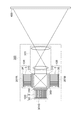
まず、本実施形態の照明装置について、図1〜図4を参照して説明する。図1は第1実施形態の照明装置の構成を示す概略斜視図、図2は導光体を示す概略斜視図、図3(a)は光源ユニットの構成を示す概略平面図、同図(b)は側面図、図4(a)は導光体ユニットに対する光源ユニットの配置を示す概略断面図、同図(b)は導光体に対する発光素子の配置を示す拡大図である。詳しくは、図4(b)は同図(a)の円で示した領域を拡大した断面図である。
(First embodiment)
<Lighting device>
First, the illuminating device of this embodiment is demonstrated with reference to FIGS. FIG. 1 is a schematic perspective view showing the configuration of the illumination device of the first embodiment, FIG. 2 is a schematic perspective view showing the light guide, FIG. 3A is a schematic plan view showing the configuration of the light source unit, and FIG. ) Is a side view, FIG. 4A is a schematic sectional view showing the arrangement of the light source unit with respect to the light guide unit, and FIG. 4B is an enlarged view showing the arrangement of the light emitting elements with respect to the light guide. Specifically, FIG. 4B is an enlarged cross-sectional view of a region indicated by a circle in FIG.
図1に示すように、本実施形態の照明装置10は、支持基板1と支持基板1上に間隔をおいて2次元配置された複数の発光素子2とを有する光源ユニット3と、光源ユニット3における複数の発光素子2のそれぞれに対応して同じく2次元配置された複数の導光体4を有する導光体ユニット5とを備えている。また、複数の導光体4を互いに空隙(間隔)を置いて2次元配置するように、複数の導光体4を支持する一対の導光体支持部6,7を有している。つまり、照明装置10は、光源ユニット3における発光素子2からの発光を導光体4を経由して射出させ、導光体ユニット5によって面状の照明を実現するものである。
As shown in FIG. 1, the
発光素子2は、発光ダイオード(LED)であって、所望の照明色に応じて白色、赤色、緑色、青色などを選択できる。また、異なる発光色が得られる発光ダイオードを組み合わせて支持基板1上に2次元配置してもよい。
The
支持基板1は、例えば、リジットで温度(熱)に対して形状安定性や耐熱性を有するセラミックなどを基体とする回路基板を用いることが好ましい。このような支持基板1には、各発光素子2を独立して発光制御可能とする配線などが形成されており、電源などを供給する外部駆動回路(図示省略)と接続される。
As the
なお、発光素子2は、発光ダイオード(LED)であることに限定されず、例えば、支持基板1として透明なガラス基板や不透明なシリコンなどの半導体基板上に複数の有機エレクトロルミネッセンス(EL)素子と、該有機EL素子を独立して発光制御可能な配線および駆動回路とが形成されたものも採用することができる。発光素子2としての有機EL素子は、公知の構成を採用することができ、高い輝度が得られる点で蛍光よりも燐光を発するものが好ましい。また、発光色も発光ダイオードと同様に白色、赤色、緑色、青色などが得られるように形成することも可能である。さらには、支持基板1上に複数の発光ダイオードを平面実装して光源ユニット3を構成する場合に比べて、発光素子2としての有機EL素子を高精細に配置可能である。また、有機EL素子は高さを発光ダイオードに比べて低く形成することができるので、薄型な光源ユニット3を実現できるという利点がある。
The
発光素子2としての発光ダイオードや有機EL素子を独立して発光制御する駆動方法としては、単純マトリックス駆動やそれぞれの発光素子2に対応してスイッチング素子を設けたアクティブマトリックス駆動を採用することができる。
As a driving method for independently controlling light emission of the light emitting diode or the organic EL element as the
導光体ユニット5は、複数の導光体4が互いに空隙(間隔)をおいて2次元配置されたものである。導光体4における光の入射側と射出側とにおいて、該空隙を一定に保持するための導光体支持部6,7が設けられている。
The
図2に示すように、導光体4は、例えば、光学的に等方で屈折率nが1よりも大きなガラスや樹脂などの透明部材からなり、断面形状が同じ四角形で互いに対向する一方の端面4aと他方の端面4bを有している。一方の端面4aにおける短辺部の長さをaとし、長辺部の長さをbとすると、一方の端面4aと他方の端面4bとの距離つまり四角柱の導光体4における光路の長さLは、上記長辺部の長さbに対して少なくとも3倍以上の長さとなっている。
一方の端面4aと他方の端面4bのどちらからでも光を入射させることが可能であるが、以降説明上、一方の端面4aを入射側の面として入射面4aと呼ぶ、したがって、一方の端面4aに対応する他方の端面4bを光の射出面4bと呼ぶこととする。
As shown in FIG. 2, the
Light can be incident from either one
次に、導光体支持部6について、図3を参照して説明する。
図3(a)および(b)に示すように、導光体支持部6は、発光素子2が設けられた支持基板1上に配設されている。導光体支持部6は、支持基板1上における発光素子2の配置に対応して設けられた開口部6aを有している。開口部6aは平面視で導光体4の入射面4aと同じ形状の四角形で、面積は入射面4aと同じかやや大きく形成されている。そして、導光体支持部6の厚み方向(支持基板1上の高さ方向)において、段差部6cを介して開口面積が開口部6aに対して一回り小さい開口部6bに接している。
Next, the
As shown in FIGS. 3A and 3B, the light
開口部6aに導光体4を挿入することにより、隣り合う導光体4は、入射面4a側において空隙(間隔)を置いて支持される。導光体支持部6の厚み方向における段差部6cの位置によって、発光素子2に対向する導光体4の入射面4aの位置を規定することができる。言い換えれば、発光素子2と入射面4aとの間の距離が一定になるように、各開口部6aにおける段差部6cの位置が決められている。
By inserting the
導光体4の射出面4b側は、図1に示したようにもう一方の導光体支持部7によって支持されている。導光体支持部7は、発光素子2の2次元配置に対応した複数の開口部7aを有している。開口部7aは、導光体4の断面形状に対して形状や大きさがほぼ同じ四角形である。導光体4の射出面4b側が開口部7aに挿入されることにより、射出面4bが全面に亘って露出すると共に、隣り合う導光体4が射出面4b側において空隙(間隔)を置いて支持される。
The
図4(a)に示すように、光源ユニット3と導光体ユニット5とは、発光素子2ごとに導光体4が一定の距離を置いて対向配置されている。導光体4の長手方向に対して直交する方向において、導光体4の間には、空隙(空気層)が存在している。
As shown in FIG. 4A, the
略点光源としての発光素子2の中心から放射状に発する光を導光体4の入射面4aに入射させると、入射した光は導光体4内を伝播する。具体的には、導光体4間は空気層となっているため、導光体4に入射した光は空気層との界面すなわち導光体4の内壁での全反射を繰り返して射出面4bから射出される。
When light emitted radially from the center of the
入射面4aおよび射出面4bの形状(導光体4の断面形状)は、図2に示した四角形に限定されず、五角形や六角形などの多角形としてもよい。当該形状を円形とすると、導光体4内を全反射して伝播する光が導光体4の光軸(断面が円形の中心を通る軸)上において集中し、射出面4bから射出された光が射出面4bの中心部で輝度が高い状態となって、平面的に輝度むらとなるおそれがある。当該形状が多角形であれば、導光体4の内壁において全反射する光の角度が変化して全反射した光が導光体4内を様々な方向に拡散しつつ伝播し、射出面4bから輝度むらが低減された状態で光を取り出せる。
The shapes of the
隣り合う導光体4間に空隙を置いて複数の導光体4を支持する導光体支持部6,7は、導光体4を支持する部分において導光体4の側面に接することになるため、接した部分から光が外部あるいは隣り合う導光体4へと漏れることがないように、光吸収性または光反射性を有していることが望ましい。
The
また、図4(b)に示すように、発光素子2から放射状に発する光は、法線方向に対する放射角度θによって必ずしも強度が一定しているわけではない。放射角度θが大きくなるに連れて放射される光の強度は弱くなる。そこで、放射状に発する光を有効に利用するため、発光素子2と導光体4との間の距離をできるだけ近くして、放射状に発した光をより多く入射面4aに入射させることが望ましい。その一方で発光素子2は発光に伴って発熱する。照明装置10としての利用ならびに発光素子2の発光寿命を考慮すると、発光素子2からの発熱を放熱させることが必要であり、発光素子2と導光体4とをある程度間隔をおいて配置することにより、効率的に上記放熱を促すことができる。
Further, as shown in FIG. 4B, the intensity of the light emitted radially from the
前述したように光源ユニット3の支持基板1上に導光体支持部6を設ける場合には、上記放熱を考慮すると、導光体支持部6は、光吸収性または光反射性を有することに加えて、熱伝導性を有する材料を選定することが望ましい。
このような導光体支持部6に適した材料としては、光吸収性と熱伝導性を有する炭素繊維などを含んだ樹脂や、光反射性と熱伝導性を有するアルミニウムなどの金属材料やその合金あるいは酸化物などが挙げられる。
As described above, when the
As a material suitable for such a light
本実施形態では、発光素子2から放射される光の有効利用と放熱とを考慮して、光強度が少なくとも半分になる放射角度θで発した光が、入射面4aに確実に入射して導光体4の内壁で反射するように、発光素子2と導光体4との距離を設定している。このように設定された当該距離以上に発光素子2と入射面4aとを離間させると、放熱の点では有利だが、光強度を稼ぐ点では不利となることは言うまでもない。
In the present embodiment, in consideration of effective use and heat dissipation of light emitted from the
なお、導光体4の長手方向の長さ(光路の長さ)Lは、上述した発光素子2と導光体4との距離(言い換えれば、入射面4aに対する光の入射角度)、入射面4aにおける長辺部の長さb、導光体4の屈折率nなどを考慮して、射出面4bにおける輝度むらが少なくなるように、例えば光学的なシミュレーションを実施して決定することができる。光学的なシミュレーションによって導かれた照明装置10の実施例について、以下に示す。
The length (length of the optical path) L in the longitudinal direction of the
(実施例1)
・発光素子2は、白色発光が得られる発光ダイオードもしくは有機EL素子。
・発光素子2からの発光における光強度が半分になる放射角度θは30度。
・導光体4は、屈折率nがおよそ1.5、入射面4aの形状が正方形で1辺の長さが1mm、導光体4間の空隙(間隔)は、およそ0.1mmである。このような導光体4の材料としては、アクリルやホウ珪酸ガラスなどが挙げられる。
このような条件で光学的なシミュレーションを実施すると、射出面4bにおける輝度むらが目立たなくなる導光体4の長さLは、2.7mm以上となる。すなわち、導光体4の長さLが入射面4aの辺部の長さの3倍程度以上となれば、輝度むらが低減された状態の照明が可能である。
Example 1
-The
The radiation angle θ at which the light intensity in the light emission from the
The
When an optical simulation is performed under such conditions, the length L of the
以上に述べた前記第1実施形態によれば、以下の効果が得られる。
(1)上記第1実施形態の照明装置10によれば、光源ユニット3のそれぞれの発光素子2から放射された光は、互いに空隙を置いて2次元配置された導光体4を伝播して射出面4bから効率よく取り出すことができる。
According to the first embodiment described above, the following effects can be obtained.
(1) According to the
(2)導光体支持部6,7は、2次元配置された導光体4間の空隙を一定に保持する。これにより、複数の導光体4からなる導光体ユニット5は、輝度むらが低減された状態で面状の照明を実現できる。また、それぞれの発光素子2を独立して発光制御することで平面的に輝度むらが少ない状態で部分照明と全面照明とを実現できる。
(2) The
(3)導光体支持部6,7は、光吸収性または光反射性を有しているので、導光体4を支持した部分における光漏れを防ぐことができる。
(3) Since the
(4)導光体支持部6は、さらに熱伝導性を有しているので、発光素子2の発光に伴う発熱を放熱して、長い発光寿命が得られる照明装置10を提供できる。
(4) Since the
(第2実施形態)
<表示装置>
次に本実施形態の表示装置について、図5〜図7を参照して説明する。図5は第2実施形態の表示装置の構成を示す概略図、図6(a)は表示デバイスとしての液晶パネルの構成を示す概略平面図、同図(b)は同図(a)のH−H’線で切った概略断面図、図7は表示装置における部分照明の例を示す概略分解斜視図である。
(Second Embodiment)
<Display device>
Next, the display device of this embodiment will be described with reference to FIGS. FIG. 5 is a schematic diagram showing the configuration of the display device according to the second embodiment, FIG. 6A is a schematic plan view showing the configuration of a liquid crystal panel as a display device, and FIG. 5B is a diagram H of FIG. FIG. 7 is a schematic exploded perspective view showing an example of partial illumination in the display device.
図5に示すように、本実施形態の表示装置100は、表示デバイスとしての受光型且つ透過型の液晶パネル110と、液晶パネル110を照明する上記第1実施形態の照明装置10とを備えている。このような表示装置100は、例えば直視型のヘッドマウントディスプレイ(HMD)に適用でき、観察者Mの左右の目線上にそれぞれ配置され、例えば観察用レンズ160を介して液晶パネル110に表示された文字や画像などの情報を確認できる構成を備えているものである。
As shown in FIG. 5, the
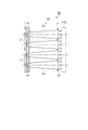
図6(a)および(b)に示すように、表示デバイスとしての液晶パネル110は、互いに対向して配置された素子基板111と素子基板111よりも平面的に一回り小さいサイズの対向基板121とを備えている。
As shown in FIGS. 6A and 6B, a
シール材140により接合された素子基板111と対向基板121との隙間(ギャップ)に、正の誘電異方性を有する液晶が充填され液晶層150を構成している。すなわち、素子基板111と対向基板121とにより液晶層150を挟持している。
A
素子基板111は、例えば、透明な石英などからなり、シール材140の外側は周辺回路領域であって、素子基板111の長手方向(X方向)の一辺に沿ってデータ線駆動回路113および外部回路と接続するための複数の実装端子117とが設けられている。また、素子基板111の短手方向(Y方向)の他の二辺に沿って、それぞれ走査線駆動回路114が設けられている。素子基板111の残る一辺に沿って、2つの走査線駆動回路114を接続する複数の配線115が設けられている。
The
素子基板111上におけるシール材140の内側には、X方向およびY方向にマトリックス状に配列した複数の画素電極112を有している。また、データ線駆動回路113と走査線駆動回路114とに電気的に接続すると共に画素電極112をスイッチング制御するスイッチング素子としてのTFT(Thin Film Transistor;図示省略)が設けられている。
Inside the sealing
対向基板121は、例えば同じく透明な石英などからなり、液晶層150側には画素電極112に対向する位置にカラーフィルター122とカラーフィルター122を画定する遮光膜123と、カラーフィルター122および遮光膜123を覆う共通電極124とが設けられている。
対向基板121に設けられた共通電極124は、図6(a)に示すように対向基板121の四隅に設けられた上下導通部116により素子基板111側の配線に電気的に接続している。
The
The
図6(a)に示すように、1つの画素は、3色のカラーフィルター122R(赤),122G(緑),122B(青)に対応した3つのサブ画素から構成されている。画素電極112はサブ画素ごとに設けられている。
3色のカラーフィルター122R,122G,122Bは、同色のカラーフィルター122がY方向に連続するように対向基板121側に設けられている。
As shown in FIG. 6A, one pixel includes three sub-pixels corresponding to the three
The three
本実施形態では、実際に表示に寄与する複数の画素の領域を表示領域110aとし、遮光膜123は、各サブ画素を区画すると共に、表示領域110aを囲んで額縁状に対向基板121側に設けられている。
In the present embodiment, a region of a plurality of pixels that actually contributes to display is defined as a
また、素子基板111と対向基板121の外側の表面(液晶層150に対して反対側の表面)にそれぞれ偏光素子としての偏光板118,126が貼り付けられている。
Polarizing
すなわち、液晶パネル110は、ストライプ方式のカラーフィルター122を備え、カラー表示を可能としたアクティブ型の液晶パネルである。
In other words, the
例えば、液晶パネル110における表示領域110aの大きさが対角0.7インチとすると、図6(a)における表示領域110aのX方向(長手方向)の長さはおよそ14.22mm、Y方向(短手方向)の長さはおよそ10.67mmとなる。このときの照明装置10における導光体ユニット5の構成例は、次の通りである。
For example, if the size of the
すなわち、導光体4の入射面4aを1辺が1.1mmの正方形とし、前述した実施例1のように、導光体4間の空隙(間隔)を0.1mmとして、長さLがおよそ3mm以上の導光体4をX方向に12本、Y方向に9本、合計108本、2次元配置して導光体ユニット5とする。光源ユニット3における発光素子2の配置は、対向する導光体4の配置に準ずることは言うまでもない。これによって、液晶パネル110の表示領域110aの形状と大きさに相当する横(X方向)14.4mm、縦(Y方向)10.8mmの領域を照明することができる。
That is, the
図7に示すように、例えば、液晶パネル110の表示領域110aにおいて、四隅の領域が明るくなる表示情報に基づいて液晶パネル110が駆動されるとき、該表示情報に対応させて、照明装置10の光源ユニット3における上記四隅の領域に対応する発光素子2を他の領域に対応する発光素子2に比べて輝度が上昇するように発光制御すれば、照明したい領域において輝度むらがない状態で部分照明を行うことができる。言い換えれば、暗くなる表示情報に基づいて、対応する発光素子2の輝度を他の発光素子2に比べて低下させてもよい。その結果、液晶パネル110の表示領域110aの全面に亘ってほぼ同じ輝度で照明する場合にくらべて、観察者Mが見たときの表示コントラストを高めることができる。このように、表示デバイスの明るさを規定する表示情報に応じて、表示デバイスを照明する照明装置の平面的な輝度を部分的に変化させて照明することは、ローカルデミングと呼ばれている。
本実施形態の表示装置100によれば、照明装置10を備え、ローカルデミングにより見栄えのよい表示品質を有するHMDを提供することができる。また、常に発光素子2を点灯させた状態とする必要がないので、消費電力を低減することができ、電源として主に電池が採用されるHMDに適している。
As shown in FIG. 7, for example, when the
According to the
(第3実施形態)
<表示装置>
次に、表示装置の他の実施形態について、図8を参照して説明する。図8は第3実施形態の表示装置の構成を示す概略図である。第3実施形態の表示装置は、表示デバイスに表示された画像などの情報を直視するものではなく、間接的に見るヘッドアップディスプレイ(HUD)である。なお、第2実施形態の表示装置100と同じ構成については、同じ符号を付し、詳細の説明は省略する。
(Third embodiment)
<Display device>
Next, another embodiment of the display device will be described with reference to FIG. FIG. 8 is a schematic diagram showing the configuration of the display device of the third embodiment. The display device according to the third embodiment does not directly view information such as an image displayed on the display device, but is a head-up display (HUD) that is viewed indirectly. In addition, about the same structure as the
図8に示すように、本実施形態の表示装置100は、第2実施形態と同様に、表示デバイスとしての受光型且つ透過型の液晶パネル110と、液晶パネル110を照明する照明装置10とを備えている。液晶パネル110の法線方向には、観察用レンズ160とハーフミラー170とが設けられている。
As shown in FIG. 8, the
照明装置10における光源ユニット3から発した光は、導光体ユニット5を経由して液晶パネル110の背面側から入射する。入射した光(照明光)は、液晶パネル110の表示情報に基づいて変調され、表示光として射出される。表示光は液晶パネル110の拡大虚像を生成するための観察用レンズ160を透過した後にハーフミラー170で反射され、観察者Mはハーフミラー170越しに文字や画像などの映像を虚像180として観察することができる。また、観察者Mは、ハーフミラー170越しに、映し出された虚像180だけでなく、前方の景色などを見ることができる。
Light emitted from the
このような表示装置100を含む表示システムは、例えば車載用のHUDとして適用され、観察者Mであるドライバーに車のスピード(速度)や道路情報などをドライバーの視線を前方に向けたまま伝えることができる。また、例えば商品ディスプレイ用のHUDとして適用され、観察者Mすなわちお客様に商品を見せるだけでなく、価格などの商品情報を知らせることができる。
輝度むらが低減され部分照明や全面照明も可能な照明装置10を備えているので、液晶パネル110に表示された文字や画像などの情報を間接的であっても観察者Mに分かり易く伝えることができる。
A display system including such a
Since the
なお、HUDとして用いる場合、表示装置100における液晶パネル110は透過型であることに限定されず、反射型であってもよい。観察用レンズ160の光軸に対して反射型の液晶パネルを交差するように配置し、導光体ユニット5から射出される照明光が液晶パネルの表示面(反射面)に入射するように照明装置10を配置する。反射型の液晶パネルにより変調され反射した光は観察用レンズ160を介してハーフミラー170で反射される。
When used as a HUD, the
(第4実施形態)
<表示装置>
次に、第4実施形態の表示装置について、図9を参照して説明する。図9は第4実施形態の表示装置の構成を示す概略図である。第4実施形態の表示装置は、表示デバイスに表示された画像などの情報を直視するものではなく、表示デバイスの表示を投影するものである。なお、第2実施形態の表示装置100と同じ構成については、同じ符号を付し、詳細の説明は省略する。
(Fourth embodiment)
<Display device>
Next, a display device according to a fourth embodiment will be described with reference to FIG. FIG. 9 is a schematic view showing the configuration of the display device of the fourth embodiment. The display device according to the fourth embodiment does not directly look at information such as an image displayed on the display device, but projects the display on the display device. In addition, about the same structure as the
図9に示すように、第4実施形態の表示装置200は、第2実施形態と同様に、表示デバイスとしての受光型且つ透過型の液晶パネル110と、液晶パネル110を照明する照明装置10と、投射用レンズ210とを備えている。
As shown in FIG. 9, the
照明装置10における光源ユニット3から発した光は、導光体ユニット5を経由して液晶パネル110の背面側から入射する。入射した光(照明光)は、液晶パネル110の表示情報に基づいて変調され、表示光として射出される。表示光は投射用レンズ210を透過することにより、前方に設けられたスクリーン250上に投射され、拡大表示される。
Light emitted from the
このような表示装置200によれば、輝度むらが低減され部分照明や全面照明も可能な照明装置10を備えているので、液晶パネル110に表示された文字や画像などの情報をスクリーン250上に高いコントラストで拡大投影して、観察者に対して視認し易い状態で情報を伝達することができる。
According to such a
(第5実施形態)
<表示装置>
次に、第5実施形態の表示装置について、図10および図11を参照して説明する。図10は第5実施形態の表示装置の構成を示す概略図、図11(a)は第5実施形態の液晶パネルの構成を示す概略平面図、同図(b)は同図(a)のJ−J’線で切った概略断面図である。第5実施形態の表示装置は、表示デバイスに表示された画像などの情報を直視するものではなく、表示デバイスの表示を投影するものである。なお、第2実施形態の表示装置100と同じ構成については、同じ符号を付し、詳細の説明は省略する。
(Fifth embodiment)
<Display device>
Next, a display device according to a fifth embodiment will be described with reference to FIGS. FIG. 10 is a schematic diagram showing the configuration of the display device of the fifth embodiment, FIG. 11A is a schematic plan view showing the configuration of the liquid crystal panel of the fifth embodiment, and FIG. 10B is the diagram of FIG. It is the schematic sectional drawing cut along the JJ 'line. The display device according to the fifth embodiment does not directly view information such as an image displayed on the display device, but projects a display on the display device. In addition, about the same structure as the
図10に示すように、本実施形態の表示装置300は、赤(R)、緑(G)、青(B)、3色の表示光のそれぞれに対応して設けられた表示ユニット301R,301G,301Bと、ダイクロイックプリズム360と、投射用レンズ370とを備えている。
As shown in FIG. 10, the
表示ユニット301Rは、表示デバイスとしての液晶パネル310と、液晶パネル310を照明する照明装置10Rとを備えている。照明装置10Rは、赤色の発光が得られる発光素子を複数備えた光源ユニット3Rと、導光体ユニット5とを有している。
他の表示ユニット301G,301Bも同様であり、表示ユニット301Gは、表示デバイスとしての液晶パネル310と、液晶パネル310を照明する照明装置10Gとを備えている。照明装置10Gは、緑色の発光が得られる発光素子を複数備えた光源ユニット3Gと、導光体ユニット5とを有している。表示ユニット301Bは、表示デバイスとしての液晶パネル310と、液晶パネル310を照明する照明装置10Bとを備えている。照明装置10Bは、青色の発光が得られる発光素子を複数備えた光源ユニット3Bと、導光体ユニット5とを有している。
The display unit 301 </ b> R includes a
The same applies to the
ダイクロイックプリズム360の3つの入射面のうちの1つに表示ユニット301Rが対向配置され、表示ユニット301Rが対向配置された入射面に対向する入射面に表示ユニット301Bが対向配置されている。残りの入射面に表示ユニット301Gが対向配置されている。つまり、表示ユニット301R,301G,301Bは、ダイクロイックプリズム360の色光ごとの入射面に対して対向配置されている。
The
ダイクロイックプリズム360は、4つの直角プリズムが貼り合わされ、その内面に赤色光を反射する誘電体多層膜と青色光を反射する誘電体多層膜とが十字状に形成されている。表示ユニット301R,301G,301Bから射出され、表示情報に基づいて変調された3つの色光は、これらの誘電体多層膜によってカラー画像を表す表示光として合成される。合成された表示光は、投射光学系である投射用レンズ370によってスクリーン400上に投射され、カラー画像が拡大されて表示される。
The
図11(a)および(b)に示すように、表示ユニット301R,301G,301Bのそれぞれに設けられた液晶パネル310は、一対の基板としての素子基板311および対向基板321と、これら一対の基板によって挟持された液晶層350とを有する。
素子基板311は対向基板321よりも一回り大きく、両基板は、シール材340を介して接合され、その隙間に負の誘電異方性を有する液晶が封入されて液晶層350を構成している。
As shown in FIGS. 11A and 11B, a
The
同図(a)に示すように、素子基板311の1辺部に沿って(X方向に)データ線駆動回路313が設けられ、これに電気的に接続された複数の端子部317が配列している。該1辺部と直交し互いに対向する他の2辺部には、該2辺部に沿って(Y方向に)走査線駆動回路314が設けられている。対向基板321を挟んで該1辺部と対向する他の1辺部には、2つの走査線駆動回路314を繋ぐ複数の配線315が設けられている。
As shown in FIG. 5A, a data
額縁状に配置されたシール材340の内側には、同じく額縁状に見切り部323が設けられている。見切り部323は、遮光性を有する金属材料あるいは樹脂材料からなり、見切り部323の内側が複数の画素を有する表示領域310aとなっている。
A
同図(b)に示すように、素子基板311の液晶層350側の表面には、画素ごとに設けられた光透過性を有する画素電極312および画素電極312をスイッチング制御するスイッチング素子としての薄膜トランジスター(図示省略)と、信号配線(図示省略)と、これらを覆う配向膜318とが形成されている。
As shown in FIG. 2B, on the surface of the
対向基板321の液晶層350側の表面には、見切り部323と、これを覆うように成膜された共通電極324と、共通電極324を覆う配向膜326とが形成されている。
On the surface of the
これらの配向膜318および配向膜326は、無機材料からなる無機配向膜であって、無機材料としてのSiO2(酸化シリコン)を斜方蒸着して得られたものである。このような配向膜318,326により挟まれた液晶層350における液晶分子は、配向膜面に対して略垂直に配向している。なお、液晶層350における液晶分子の配向状態はこれに限定されるものではなく、略水平配向としてもよい。
The
対向基板321に設けられた共通電極324は、同図(a)に示すように対向基板321の四隅に設けられた上下導通部316により素子基板311側の配線に電気的に接続している。
The
なお、液晶パネル310は、各表示ユニット310R,301G,301Bにおいて、光の入射側と射出側とに偏光素子を光学的にノーマリーブラックとなるように配置して用いられるが、図10および図11では図示省略している。
Note that the
各表示ユニット301R,301G,301Bは、それぞれ色光に対応した発光素子を有する光源ユニット3R,3G,3Bを備えているので、照明される液晶パネル310は、第2実施形態の液晶パネル110に対してカラーフィルター122が不要な構成となっている。
Each of the
このような表示装置300によれば、白色光源を色光に分離して照明光とする例えばダイクロイックミラーのような光学系を必要とせず、個々の色光に対応した照明装置10R,10G,10Bを備えているので、ローカルデミングの駆動方法を用いれば、明るく且つコントラストが高い映像を投射表示できる。
According to such a
上記実施形態以外にも様々な変形例が考えられる。以下、変形例を挙げて説明する。 Various modifications other than the above embodiment are conceivable. Hereinafter, a modification will be described.
(変形例1)上記第1実施形態の照明装置10において、導光体4の構成は、これに限定されない。図12は変形例の導光体を示す斜視図、図13は変形例の導光体を備えた照明装置を示す概略断面図である。例えば、図12に示すように、変形例の導光体41は、四角形(正方形)の入射面42と、入射面42に対向する同じく四角形(正方形)の射出面43とを有する。射出面43の面積は入射面42の面積よりも大きい、すなわち、それぞれの辺部の長さは、a<a’、b<b’となっている。導光体41の光路の長さLは、入射面42の辺部のうち長い方の長さのおよそ3倍以上となっている。すなわち、この変形例では、L≧3bとなっている。
図13に示すように、照明装置50は、支持基板1上に2次元配置された複数の発光素子2と、支持基板1上に配置された一方の導光体支持部6と、発光素子2のそれぞれに入射面42が対向配置された複数の導光体41を有する導光体ユニット45と、導光体ユニット45の射出面43側において、複数の導光体41を空隙(間隔)をおいて支持する他方の導光体支持部7とを備えている。
導光体41の入射面42に入射した光は、導光体41の内壁で全反射して伝播する。射出面43は、前述したように入射面42に比べて面積が大きいので、導光体41の内壁で全反射するときの角度が第1実施形態の導光体4に比べて小さくなる。したがって、導光体41の射出面43から射出する光は、導光体4に比べて射出面43の法線方向(光軸)に近づいた状態となり、射出面43から指向性が高い光が取り出される。それゆえに、射出面43側に液晶パネル110を対向配置すれば、液晶パネル110の表示領域に対してより選択的な照明が可能となる。言い換えれば、選択された領域以外に照明光があたることを抑えて、より効果的に部分照明することができる。
(Modification 1) In the
As shown in FIG. 13, the
The light incident on the
(変形例2)上記第1実施形態の照明装置10では、複数の発光素子2を支持基板1の辺部に沿って縦方向と横方向とに2次元配置し、これに対応して複数の導光体4も空隙(間隔)を置いて2次元配置したが、これに限定されない。例えば、発光素子2を有機EL素子として支持基板1上において上記縦方向または横方向に線状に形成して線光源とする。導光体4は、上記線光源から発した光が効率的に入射するように、上記線光源と同様に上記縦方向または上記横方向に連続する入射面4a(射出面4b)を有する構成とする。このような導光体4は、線光源の方向と直交する方向において空隙(間隔)を置いて配置される。これによれば、部分照明が可能な領域が上記第1実施形態に比べて疎な状態となるものの、ローカルデミングにおける発光素子2の発光制御を液晶パネル110の表示領域110aにおける行方向または列方向の表示情報に対応させて簡略化できる。
(Modification 2) In the illuminating
(変形例3)上記第1実施形態における照明装置10において、一方の導光体支持部6の構成は、これに限定されない。例えば、導光体4を互いに空隙(間隔)を置いて支持可能であれば、導光体4の入射面4a側を収納する開口部6aを有した一体構造である必要はない。つまり、導光体4間に位置して支持基板1上に立設された複数の独立した構造物でもよい。このような構成にすれば、支持基板1上において構造物間に空間が生まれ、発光素子2からの熱を効率よく放熱できる。また、該構造物が必ずしも熱伝導体である必要がなくなるので、材料選択の余地が広がる。
(Modification 3) In the
(変形例4)上記第2実施形態において観察者Mの左右の目線上に配置される表示装置100において、液晶パネル110に表示される画像情報を左目用と右目用とに対応させた表示とすれば、観察者Mは立体表示を楽しむことができる。つまり、立体表示が可能なHMDとしての表示装置100を提供できる。
(Modification 4) In the
(変形例5)上記第1実施形態の照明装置10によって照明される表示デバイスは、液晶パネル110(液晶パネル310)に限定されず、背面から照明される受光型の表示デバイスであれば良い。
(Modification 5) The display device illuminated by the
1…支持基板、2…発光素子、3…光源ユニット、4…導光体、4a…一方の端面あるいは入射面、4b…他方の端面あるいは射出面、5…導光体ユニット、6,7…導光体支持部、10,10R,10G,10B…照明装置、41…導光体、42…入射面、43…射出面、45…導光体ユニット、50…照明装置、100,200,300…表示装置、110,310…表示デバイスとしての液晶パネル、301R,301G,301B…表示ユニット。
DESCRIPTION OF
Claims (11)
前記導光体ごとの前記一方の端面に対して間隔をおいて対向配置された少なくとも1つの発光素子を含む光源ユニットと、を備えたことを特徴とする照明装置。 A light guide unit having a polygonal cross-sectional shape and two-dimensionally arranged light guides having one end face and the other end face facing each other with a gap;
And a light source unit including at least one light-emitting element disposed to face the one end face of each light guide at an interval.
前記一方の端面側に位置する前記導光体支持部は、前記支持基板上に配設されていることを特徴とする請求項4または5に記載の照明装置。 The light source unit has a support substrate on which a plurality of the light emitting elements are arranged,
The lighting device according to claim 4, wherein the light guide support portion positioned on the one end face side is disposed on the support substrate.
前記照明装置の前記導光体ユニットにおける前記他方の端面に対して間隔を置いて対向配置された受光型の表示デバイスと、を備えたことを特徴とする表示装置。 The lighting device according to any one of claims 1 to 9,
And a light-receiving display device disposed opposite to the other end face of the light guide unit of the illumination device.
複数の前記表示ユニットのそれぞれの表示光を合成して表示が行われることを特徴とする請求項10に記載の表示装置。 A plurality of display units including the lighting device and the display device;
The display device according to claim 10, wherein display is performed by combining display lights of the plurality of display units.
Priority Applications (1)
| Application Number | Priority Date | Filing Date | Title |
|---|---|---|---|
| JP2010141381A JP2012009154A (en) | 2010-06-22 | 2010-06-22 | Lighting system and display device |
Applications Claiming Priority (1)
| Application Number | Priority Date | Filing Date | Title |
|---|---|---|---|
| JP2010141381A JP2012009154A (en) | 2010-06-22 | 2010-06-22 | Lighting system and display device |
Publications (1)
| Publication Number | Publication Date |
|---|---|
| JP2012009154A true JP2012009154A (en) | 2012-01-12 |
Family
ID=45539495
Family Applications (1)
| Application Number | Title | Priority Date | Filing Date |
|---|---|---|---|
| JP2010141381A Withdrawn JP2012009154A (en) | 2010-06-22 | 2010-06-22 | Lighting system and display device |
Country Status (1)
| Country | Link |
|---|---|
| JP (1) | JP2012009154A (en) |
Cited By (8)
| Publication number | Priority date | Publication date | Assignee | Title |
|---|---|---|---|---|
| JP2016500466A (en) * | 2012-12-20 | 2016-01-12 | チザラ リヒトシステーメ ゲーエムベーハーZizala Lichtsysteme GmbH | Floodlight unit with light guide unit for floodlight |
| JP2016212962A (en) * | 2015-04-30 | 2016-12-15 | 日亜化学工業株式会社 | Luminaire |
| JP2017037109A (en) * | 2015-08-07 | 2017-02-16 | マックス株式会社 | Light-emitting display device and air compressor |
| JP2017111341A (en) * | 2015-12-17 | 2017-06-22 | 株式会社テクノポスト | Luminaire |
| JP2019003762A (en) * | 2017-06-13 | 2019-01-10 | 株式会社テクノポスト | Luminaire |
| WO2020080022A1 (en) * | 2018-10-16 | 2020-04-23 | ソニー株式会社 | Display device |
| JP2021096978A (en) * | 2019-12-18 | 2021-06-24 | ミネベアミツミ株式会社 | Planar lighting device |
| US11880016B2 (en) | 2020-04-10 | 2024-01-23 | Nichia Corporation | Light emitting device |
-
2010
- 2010-06-22 JP JP2010141381A patent/JP2012009154A/en not_active Withdrawn
Cited By (8)
| Publication number | Priority date | Publication date | Assignee | Title |
|---|---|---|---|---|
| JP2016500466A (en) * | 2012-12-20 | 2016-01-12 | チザラ リヒトシステーメ ゲーエムベーハーZizala Lichtsysteme GmbH | Floodlight unit with light guide unit for floodlight |
| JP2016212962A (en) * | 2015-04-30 | 2016-12-15 | 日亜化学工業株式会社 | Luminaire |
| JP2017037109A (en) * | 2015-08-07 | 2017-02-16 | マックス株式会社 | Light-emitting display device and air compressor |
| JP2017111341A (en) * | 2015-12-17 | 2017-06-22 | 株式会社テクノポスト | Luminaire |
| JP2019003762A (en) * | 2017-06-13 | 2019-01-10 | 株式会社テクノポスト | Luminaire |
| WO2020080022A1 (en) * | 2018-10-16 | 2020-04-23 | ソニー株式会社 | Display device |
| JP2021096978A (en) * | 2019-12-18 | 2021-06-24 | ミネベアミツミ株式会社 | Planar lighting device |
| US11880016B2 (en) | 2020-04-10 | 2024-01-23 | Nichia Corporation | Light emitting device |
Similar Documents
| Publication | Publication Date | Title |
|---|---|---|
| US8373630B2 (en) | Display device | |
| JP4227592B2 (en) | Equipment for image generation | |
| JP4600218B2 (en) | Surface light source and liquid crystal display device | |
| JP4655465B2 (en) | Surface light source and liquid crystal display device | |
| JP2012009154A (en) | Lighting system and display device | |
| US11294173B2 (en) | Display device and head-up display device | |
| US20120306861A1 (en) | Light source device and display | |
| US20090174700A1 (en) | Illuminator for emitting at least two lights having directivity and display apparatus using same | |
| WO2013069405A1 (en) | Illumination device, display device and electronic device | |
| CN105829947A (en) | Liquid-crystal display for heads-up display, and heads-up display | |
| WO2011068072A1 (en) | Light diffusion sheet, display panel, and display device | |
| WO2013069406A1 (en) | Display device and electronic device | |
| KR101940946B1 (en) | Head-up display device | |
| JP4793191B2 (en) | LIGHTING DEVICE, LIQUID CRYSTAL DEVICE, AND ELECTRONIC DEVICE | |
| KR20210016638A (en) | Hybrid backlight, display, and method | |
| US20220404540A1 (en) | Illumination apparatus | |
| KR20170094809A (en) | Display device | |
| JP6749824B2 (en) | Display device and lighting device | |
| JP2012252937A (en) | Light source device and display device | |
| JP4483233B2 (en) | Surface light source and liquid crystal display device | |
| JP4501625B2 (en) | Surface light source and liquid crystal display device | |
| JP4780224B2 (en) | Display device | |
| JP2005077472A (en) | Liquid crystal display | |
| KR102481786B1 (en) | Backlight unit and liquid crystal display device having the same | |
| JP2008071856A (en) | Light source, illuminator, liquid crystal device, and electronic apparatus |
Legal Events
| Date | Code | Title | Description |
|---|---|---|---|
| A300 | Application deemed to be withdrawn because no request for examination was validly filed |
Free format text: JAPANESE INTERMEDIATE CODE: A300 Effective date: 20130903 |