JP2016220445A - Voltage control device for power storage module, and voltage control method - Google Patents
Voltage control device for power storage module, and voltage control method Download PDFInfo
- Publication number
- JP2016220445A JP2016220445A JP2015104545A JP2015104545A JP2016220445A JP 2016220445 A JP2016220445 A JP 2016220445A JP 2015104545 A JP2015104545 A JP 2015104545A JP 2015104545 A JP2015104545 A JP 2015104545A JP 2016220445 A JP2016220445 A JP 2016220445A
- Authority
- JP
- Japan
- Prior art keywords
- power storage
- voltage
- storage elements
- storage module
- vuse
- Prior art date
- Legal status (The legal status is an assumption and is not a legal conclusion. Google has not performed a legal analysis and makes no representation as to the accuracy of the status listed.)
- Pending
Links
Images


Classifications
-
- Y—GENERAL TAGGING OF NEW TECHNOLOGICAL DEVELOPMENTS; GENERAL TAGGING OF CROSS-SECTIONAL TECHNOLOGIES SPANNING OVER SEVERAL SECTIONS OF THE IPC; TECHNICAL SUBJECTS COVERED BY FORMER USPC CROSS-REFERENCE ART COLLECTIONS [XRACs] AND DIGESTS
- Y02—TECHNOLOGIES OR APPLICATIONS FOR MITIGATION OR ADAPTATION AGAINST CLIMATE CHANGE
- Y02E—REDUCTION OF GREENHOUSE GAS [GHG] EMISSIONS, RELATED TO ENERGY GENERATION, TRANSMISSION OR DISTRIBUTION
- Y02E60/00—Enabling technologies; Technologies with a potential or indirect contribution to GHG emissions mitigation
- Y02E60/10—Energy storage using batteries
Abstract
Description
本発明は、直列に接続されたn個(2≦n)の蓄電素子B(i)(iは1からnの整数)を含む蓄電モジュールの電圧制御装置および電圧制御方法に関する。 The present invention relates to a voltage control device and a voltage control method for a power storage module including n (2 ≦ n) power storage elements B (i) (i is an integer from 1 to n) connected in series.
蓄電モジュールの多くは、直列に接続された複数の蓄電素子を含んでいる。複数の蓄電素子は、全く同じ特性を有するわけではなく、それぞれ独自の特性を有している。これは製造時の条件のバラツキ、劣化の進行度の相違など、不可避な原因に基づいている。そのため、例えば、直列に接続された複数の蓄電素子のうち最も容量の小さい蓄電素子は、過充電または過放電となりやすく、劣化が進行しやすい。その結果、蓄電素子間の特性のバラツキが益々大きくなってしまう。 Many power storage modules include a plurality of power storage elements connected in series. The plurality of power storage elements do not have exactly the same characteristics, but have their own characteristics. This is based on inevitable causes such as variations in manufacturing conditions and differences in the degree of deterioration. Therefore, for example, a storage element with the smallest capacity among a plurality of storage elements connected in series is likely to be overcharged or overdischarged, and deterioration is likely to proceed. As a result, the variation in characteristics between the power storage elements becomes larger.
そこで、特許文献1は、蓄電素子の現在電圧の均等化を行うことを提案している。
Therefore,
通常、直列に接続された複数の蓄電素子を含む蓄電モジュールの電圧は、使用下限電圧Vuse-ud以上、使用上限電圧Vuse-up以下に制御されている。現在電圧を均等化したとしても、Vuse-udまたはVuse-upの付近では、電圧にバラツキが発生する。このようなバラツキを考慮せずに、使用したい電圧範囲の上下限まで蓄電モジュールを充放電すると、容量の小さい蓄電素子の劣化が進行してしまう。 Usually, the voltage of a power storage module including a plurality of power storage elements connected in series is controlled to be not less than the use lower limit voltage Vuse-ud and not more than the use upper limit voltage Vuse-up. Even if the current voltage is equalized, the voltage varies in the vicinity of Vuse-ud or Vuse-up. If the power storage module is charged / discharged up to the upper and lower limits of the voltage range to be used without considering such variations, the deterioration of the power storage element having a small capacity proceeds.
上記のような劣化を抑制する観点から、複数の蓄電素子の電圧を、それぞれ個別に、動作保障下限電圧Vm-ud以上、動作保障上限電圧Vm-up以下になるように制限することもできる。しかし、最初に上下限電圧に達した蓄電素子により、蓄電モジュールの全体の充放電範囲が制限を受ける。これにより、蓄電モジュールが本来備える容量を有効活用できなくなる。 From the viewpoint of suppressing the deterioration as described above, the voltages of the plurality of power storage elements can be individually limited to be not less than the operation guarantee lower limit voltage Vm-ud and not more than the operation guarantee upper limit voltage Vm-up. However, the entire charge / discharge range of the power storage module is limited by the power storage element that first reaches the upper and lower limit voltages. As a result, the capacity originally provided in the power storage module cannot be effectively used.
また、現在電圧の均等化は、電圧の高い蓄電素子を選択的に放電することにより行われる。よって、均等化された電圧は、常に現在電圧より低く、均等化目標電圧の選択の幅は小さくなる。 Further, equalization of the current voltage is performed by selectively discharging a storage element having a high voltage. Therefore, the equalized voltage is always lower than the current voltage, and the selection range of the equalization target voltage is small.
上記に鑑み、本発明の一局面は、直列に接続されたn個(2≦n)の蓄電素子B(i)(iは1からnの整数)を含む蓄電モジュールと、前記蓄電モジュールの電圧を使用下限電圧Vuse-ud以上、使用上限電圧Vuse-up以下に制御する第1制御部と、前記n個の蓄電素子B(i)の電圧をそれぞれ個別に動作保障下限電圧Vm-ud以上、動作保障上限電圧Vm-up以下に制御する第2制御部と、均等化目標電圧Vm(ただし、Vm-ud≦Vm≦Vm-up)に基づいて、前記n個の蓄電素子B(i)の設定電圧Vs(i)(ただし、Vm≠V(i))をそれぞれ個別に求める計算部と、前記Vs(i)に向けて、前記n個の蓄電素子B(i)の少なくとも一部をそれぞれ個別に充電または放電する充放電制御部と、を具備し、前記計算部は、前記n個の蓄電素子B(i)が前記Vmで均等化されるように前記Vs(i)を算出する、蓄電モジュールの電圧制御装置に関する。 In view of the above, one aspect of the present invention is a storage module including n (2 ≦ n) storage elements B (i) (i is an integer from 1 to n) connected in series, and the voltage of the storage module A first control unit for controlling the voltage of the n power storage elements B (i) to be equal to or higher than the use lower limit voltage Vuse-ud and lower than the use upper limit voltage Vuse-up. Based on the second control unit that controls the operation guaranteed upper limit voltage Vm-up or less and the equalization target voltage Vm (where Vm-ud ≦ Vm ≦ Vm-up), the n power storage elements B (i) A calculation unit that individually obtains a set voltage Vs (i) (where Vm ≠ V (i)), and at least a part of the n power storage elements B (i) toward the Vs (i) A charge / discharge control unit that individually charges or discharges, wherein the calculation unit includes the n power storage elements B (i). The present invention relates to a voltage control device for a power storage module that calculates Vs (i) so as to be equalized by Vm.
本発明の別の局面は、(I)直列に接続されたn個(2≦n)の蓄電素子B(i)(iは1からnの整数)を含む蓄電モジュールの電圧を、使用下限電圧Vuse-ud以上、使用上限電圧Vuse-up以下に制御する工程と、(II)前記n個の蓄電素子B(i)の電圧をそれぞれ個別に動作保障下限電圧Vm-ud以上、動作保障上限電圧Vm-up以下に制御する工程と、(III)均等化目標電圧Vm(ただし、Vm-ud≦Vm≦Vm-up)に基づいて、前記n個の蓄電素子B(i)の設定電圧Vs(i)(ただし、Vm≠Vs(i))をそれぞれ個別に求める工程と、(IV)前記Vs(i)に向けて、前記n個の蓄電素子B(i)の少なくとも一部をそれぞれ個別に充電または放電する工程と、を具備し、前記Vs(i)は、前記n個の蓄電素子B(i)が前記Vmで均等化されるように算出される、蓄電モジュールの電圧制御方法に関する。 According to another aspect of the present invention, (I) the voltage of a power storage module including n (2 ≦ n) power storage elements B (i) connected in series (i is an integer from 1 to n) A step of controlling the voltage to Vuse-ud or more and the use upper limit voltage Vuse-up or less; and (II) the voltage of the n power storage elements B (i) is individually set to the operation guarantee lower limit voltage Vm-ud or more and the operation guarantee upper limit voltage. And (III) a set voltage Vs (n) of the n power storage elements B (i) based on the equalization target voltage Vm (where Vm-ud ≦ Vm ≦ Vm-up). i) (however, Vm ≠ Vs (i)) is obtained individually, and (IV) at least a part of the n power storage elements B (i) is individually provided toward Vs (i). Charging or discharging, and the Vs (i) is calculated so that the n power storage elements B (i) are equalized by the Vm. The present invention relates to a voltage control method for a storage module.
本発明の上記局面によれば、蓄電モジュールの全体の電圧を使用下限電圧Vuse-ud以上、使用上限電圧Vuse-up以下に制御し、かつ、複数の蓄電素子の電圧をそれぞれ個別に動作保障下限電圧Vm-ud以上、動作保障上限電圧Vm-up以下になるように制限しつつ、蓄電モジュールが本来備える容量を、より有効に活用することができる。 According to the above aspect of the present invention, the overall voltage of the power storage module is controlled to be not less than the use lower limit voltage Vuse-ud and not more than the use upper limit voltage Vuse-up, and the voltages of the plurality of power storage elements are individually set to the operation guarantee lower limit. The capacity originally provided in the power storage module can be utilized more effectively while limiting the voltage to be not less than the voltage Vm-ud and not more than the operation guarantee upper limit voltage Vm-up.
[発明の実施形態の説明]
最初に発明の実施形態の内容を列記して説明する。
本実施形態に係る蓄電モジュールの電圧制御装置は、直列に接続されたn個(2≦n)の蓄電素子B(i)(iは1からnの整数)を含む蓄電モジュールと、蓄電モジュールの電圧を使用下限電圧Vuse-ud以上、使用上限電圧Vuse-up以下に制御する第1制御部と、n個の蓄電素子の電圧をそれぞれ個別に動作保障下限電圧Vm-ud以上、動作保障上限電圧Vm-up以下に制御する第2制御部と、均等化目標電圧Vm(ただし、Vm-ud≦Vm≦Vm-up)に基づいて、n個の蓄電素子の設定電圧Vs(i)(ただし、Vm≠Vs(i))をそれぞれ個別に求める計算部と、Vs(i)に向けて、n個の蓄電素子の少なくとも一部をそれぞれ個別に充電または放電する充放電制御部とを具備する。
[Description of Embodiment of the Invention]
First, the contents of the embodiments of the invention will be listed and described.
A voltage control device for a power storage module according to the present embodiment includes a power storage module including n (2 ≦ n) power storage elements B (i) (i is an integer from 1 to n) connected in series, The first control unit that controls the voltage to the use lower limit voltage Vuse-ud or more and the use upper limit voltage Vuse-up or less, and the voltages of the n power storage elements individually to the operation guarantee lower limit voltage Vm-ud and the operation guarantee upper limit voltage, respectively. Based on the second control unit that controls Vm-up or less and the equalization target voltage Vm (where Vm-ud ≦ Vm ≦ Vm-up), the set voltage Vs (i) of n power storage elements (however, Vm ≠ Vs (i)) are individually calculated, and a charging / discharging control unit that individually charges or discharges at least a part of the n power storage elements toward Vs (i) is provided.
計算部は、n個の蓄電素子がVmで均等化されるように、Vs(i)を算出する。ここで、n個の蓄電素子がVmで均等化されるとは、例えばn個の蓄電素子の電圧が、同時に、Vm(またはVm近傍の電圧)になることを意味する。 The calculation unit calculates Vs (i) so that n power storage elements are equalized by Vm. Here, the n power storage elements being equalized by Vm means that, for example, the voltages of the n power storage elements simultaneously become Vm (or a voltage in the vicinity of Vm).
Vmは、例えばVm-ud(またはVm-udの近傍の電圧)またはVm-up(またはVm-upの近傍の電圧)に設定される。これにより、n個の蓄電素子の電圧は、大きくばらつくことなく、Vm-udまたはVm-upで均等化される。よって、高電圧領域または低電圧領域で、第2制御部による制限を受けにくくなり、蓄電モジュールのVuse-ud以上、Vuse-up以下の電圧範囲を、より有効に活用できるようになる。 For example, Vm is set to Vm-ud (or a voltage near Vm-ud) or Vm-up (or a voltage near Vm-up). As a result, the voltages of the n power storage elements are equalized by Vm-ud or Vm-up without greatly varying. Therefore, it becomes difficult to be restricted by the second control unit in the high voltage region or the low voltage region, and the voltage range of Vuse-ud or more and Vuse-up or less of the power storage module can be used more effectively.
ただし、例えばVmをVm-upに設定すると、低電圧領域では電圧のバラツキが大きくなる可能性がある。逆に、VmをVm-udに設定すると、高電圧領域で電圧のバラツキが大きくなる可能性がある。よって、Vmは、蓄電モジュールの用途や制御の目的に適するように選択される。例えば、過放電を防止する要請が大きい場合には、VmをVm-ud(またはVm-udの近傍の電圧)に設定すればよい。 However, for example, when Vm is set to Vm-up, there is a possibility that the voltage variation becomes large in the low voltage region. On the other hand, when Vm is set to Vm-ud, there is a possibility that the voltage variation becomes large in the high voltage region. Therefore, Vm is selected so as to be suitable for the use of the power storage module and the purpose of control. For example, when there is a great demand for preventing overdischarge, Vm may be set to Vm-ud (or a voltage in the vicinity of Vm-ud).
なお、Vx(=Vm、Vm-upまたはVm-ud)の近傍の電圧とは、例えばVx±Vx/100の電圧範囲(すなわち0.99Vx〜1.01Vx)である。すなわち、均等化目標電圧Vmを、例えば2Vに設定する場合、±20mV程度の均等化電圧のバラツキは許容される。 The voltage in the vicinity of Vx (= Vm, Vm-up or Vm-ud) is, for example, a voltage range of Vx ± Vx / 100 (that is, 0.99 Vx to 1.01 Vx). That is, when the equalization target voltage Vm is set to 2 V, for example, a variation in the equalization voltage of about ± 20 mV is allowed.
計算部は、例えば、n個の蓄電素子B(i)の現在電圧Vr(i)における蓄電量の差ΔQrが、Vmにおける蓄電量の差ΔQmに近づくように、Vs(i)を計算すればよい。すなわち、均等化により、Vs(i)におけるn個の蓄電素子B(i)の蓄電量の差は、ΔQmに近づく(もしくはΔQmに等しくなる)。ΔQrおよびΔQmは、例えば、n個の蓄電素子のうち、基準となる1つの蓄電素子B(base)と他の蓄電素子との各電圧における蓄電量の差であり、それぞれ(n−1)個のΔQrおよびΔQmが算出される。 For example, if the calculation unit calculates Vs (i) such that the difference ΔQr in the storage amount at the current voltage Vr (i) of the n storage elements B (i) approaches the difference ΔQm in the storage amount at Vm. Good. That is, due to equalization, the difference in the amount of power stored in the n power storage elements B (i) at Vs (i) approaches (or becomes equal to) ΔQm. ΔQr and ΔQm are, for example, the difference in the amount of electricity stored in each voltage between one reference storage element B (base) and the other storage element among n storage elements, and each is (n−1). ΔQr and ΔQm are calculated.
n個の蓄電素子B(i)のVmにおける蓄電量の差ΔQmと、Vs(i)における蓄電量の差とは大きく相違しない。すなわち、その後の充放電は、Vs(i)における蓄電量の差をほぼ維持した状態で行われる。直列に接続されているn個の蓄電素子B(i)にはそれぞれ同じ電流が流れるため、充放電時の蓄電量の増減も同じになる。よって、蓄電量の差に基づく均等化処理の信頼性は高い。 The difference ΔQm in the storage amount at Vm of the n storage elements B (i) and the difference in the storage amount at Vs (i) are not significantly different. That is, the subsequent charging / discharging is performed in a state in which the difference in the storage amount in Vs (i) is substantially maintained. Since the same current flows through each of the n power storage elements B (i) connected in series, the increase or decrease in the amount of power stored during charge / discharge is the same. Therefore, the reliability of the equalization process based on the difference in the charged amount is high.
上記電圧制御装置は、n個の蓄電素子が、それぞれキャパシタである場合に特に有効である。n個の蓄電素子が、それぞれキャパシタである場合、計算部は、n個の蓄電素子の電圧(またはSOC)と静電容量との相関関係を利用して、ΔQrおよびΔQmを算出することができる。キャパシタは、その電圧(またはSOC)から静電容量を比較的正確に導くことができる。 The voltage control device is particularly effective when n power storage elements are each capacitors. When each of the n power storage elements is a capacitor, the calculation unit can calculate ΔQr and ΔQm using the correlation between the voltage (or SOC) of the n power storage elements and the capacitance. . A capacitor can derive its capacitance relatively accurately from its voltage (or SOC).
なお、蓄電素子のVmにおける実際の蓄電量は、蓄電素子の電圧(またはSOC)と静電容量との相関関係を利用して求められるVmにおける蓄電量Qmに対して、例えば±2%程度のバラツキが許容される。 Note that the actual storage amount at Vm of the storage element is, for example, about ± 2% with respect to the storage amount Qm at Vm obtained using the correlation between the voltage (or SOC) of the storage element and the capacitance. Variations are allowed.
次に、本実施形態に係る蓄電モジュールの電圧制御方法は、(I)直列に接続されたn個(2≦n)の蓄電素子B(i)(iは1からnの整数)を含む蓄電モジュールの電圧を、使用下限電圧Vuse-ud以上、使用上限電圧Vuse-up以下に制御する工程と、(II)n個の蓄電素子B(i)の電圧をそれぞれ個別に動作保障下限電圧Vm-ud以上、動作保障上限電圧Vm-up以下に制御する工程と、(III)均等化目標電圧Vm(ただし、Vm-ud≦Vm≦Vm-up)に基づいて、n個の蓄電素子B(i)の設定電圧Vs(i)(ただし、Vm≠Vs(i))をそれぞれ個別に求める工程と、(IV)Vs(i)に向けて、n個の蓄電素子B(i)の少なくとも一部をそれぞれ個別に充電または放電する工程とを具備する。ここでも、Vs(i)は、n個の蓄電素子B(i)がVmで均等化されるように算出される。上記方法によれば、蓄電モジュールが本来備える容量を、より有効に活用することができる。なお、工程(III)では、Vs(i)を算出する際に適切なVmを設定してもよく、予め設定されたVmを使用してもよい。 Next, the voltage control method of the power storage module according to the present embodiment includes (I) power storage including n (2 ≦ n) power storage elements B (i) (i is an integer from 1 to n) connected in series. The step of controlling the voltage of the module between the use lower limit voltage Vuse-ud and the use upper limit voltage Vuse-up, and (II) the voltage of the n power storage elements B (i) individually for the operation guarantee lower limit voltage Vm- Based on the step of controlling ud to the operation guarantee upper limit voltage Vm-up and below (III) equalization target voltage Vm (where Vm-ud ≦ Vm ≦ Vm-up), n power storage elements B (i ) Of the set voltage Vs (i) (where Vm ≠ Vs (i)), and (IV) at least part of the n power storage elements B (i) toward Vs (i) And charging or discharging each of them individually. Again, Vs (i) is calculated so that n power storage elements B (i) are equalized by Vm. According to the above method, the capacity originally provided in the power storage module can be utilized more effectively. In step (III), an appropriate Vm may be set when Vs (i) is calculated, or a preset Vm may be used.
工程(III)は、例えば、n個の蓄電素子B(i)のVmにおける蓄電量の差ΔQmを計算する工程と、n個の蓄電素子B(i)の現在電圧Vr(i)をそれぞれ測定し、n個の蓄電素子B(i)のVr(i)における蓄電量の差ΔQrを計算する工程と、ΔQrが、ΔQmに近づくように、Vs(i)を算出する工程とを具備する。 In step (III), for example, a step of calculating a difference ΔQm in the amount of electricity stored in Vm of n power storage elements B (i) and a current voltage Vr (i) of n power storage elements B (i) are measured. And a step of calculating the difference ΔQr in the amount of electricity stored in Vr (i) of n power storage elements B (i) and a step of calculating Vs (i) so that ΔQr approaches ΔQm.
n個の蓄電素子B(i)が、それぞれキャパシタである場合、工程(III)は、n個の蓄電素子B(i)の電圧またはSOCと静電容量との関係を利用して、ΔQrおよびΔQmを算出する工程を含むことが好ましい。 When n power storage elements B (i) are each capacitors, step (III) uses ΔVr and the relationship between the voltage or SOC of the n power storage elements B (i) and the capacitance. It is preferable to include a step of calculating ΔQm.
n個の蓄電素子B(i)の劣化状態に応じて、適時に、電圧またはSOCと静電容量との関係をリセットしてもよく、更に、適時に、Vmをリセットしてもよい。これにより、蓄電量の差に基づく均等化処理の信頼性を、更に高めることができる。 Depending on the deterioration state of the n power storage elements B (i), the relationship between the voltage or the SOC and the capacitance may be reset in a timely manner, and Vm may be reset in a timely manner. Thereby, the reliability of the equalization process based on the difference in the charged amount can be further increased.
[発明の実施形態の詳細]
本発明の実施形態を、適宜図面を参照しつつ以下に説明する。なお、本発明はこれらの例示に限定されるものではなく、添付の特許請求の範囲によって示され、特許請求の範囲と均等の意味および範囲内での全ての変更が含まれることが意図される。
[Details of the embodiment of the invention]
Embodiments of the present invention will be described below with reference to the drawings as appropriate. In addition, this invention is not limited to these illustrations, is shown by the attached claim, and is intended that all the changes within the meaning and range equivalent to the claim are included. .
図1に、本実施形態に係る電圧制御装置の一例の回路構成図を示す。
電圧制御装置100は、直列に接続されたn個(2≦n)の蓄電素子B(i)(iは1からnの整数)を含む蓄電モジュール101を具備する。蓄電素子B(1)〜B(n)には、それぞれ均等化処理のための抵抗R(1)〜R(n)とスイッチS(1)〜S(n)とが並列に接続されている。
FIG. 1 shows a circuit configuration diagram of an example of a voltage control apparatus according to the present embodiment.
The
蓄電モジュール101は、モジュール制御部102と連絡し合っている。モジュール制御部102は、蓄電モジュールの電圧を使用下限電圧Vuse-ud以上、使用上限電圧Vuse-up以下に制御する第1制御部11と、蓄電素子B(1)〜B(n)の電圧をそれぞれ個別に動作保障下限電圧Vm-ud以上、動作保障上限電圧Vm-up以下に制御する第2制御部12と、スイッチS(1)〜S(n)をそれぞれ個別に操作するスイッチ制御部13とを具備する。第1制御部11は、蓄電モジュールの電圧を検出する第1電圧センサ(図示せず)を具備する。第2制御部12は、蓄電素子B(1)〜B(n)の電圧をそれぞれ個別に検出する第2電圧センサを具備する。スイッチ制御部(SW制御部)13は、スイッチS(1)〜S(n)をそれぞれ個別に操作することで、蓄電素子B(1)〜B(n)をそれぞれ個別に任意の時間だけ充電または放電できるように構成されている。
The power storage module 101 communicates with the
なお、抵抗およびスイッチの数および接続方法は、図1の例に限られない。蓄電素子B(1)〜B(n)を、それぞれ個別に充電または放電できる構成であればよい。蓄電素子B(1)〜B(n)は、キャパシタ、二次電池などのデバイスである。キャパシタは、電気二重層キャパシタ、リチウムイオンキャパシタなどであり得る。二次電池は、ナトリウムイオン二次電池、リチウムイオン二次電池、ニッケル水素蓄電池などであり得る。スイッチS(1)〜S(n)の種類は、特に限定されず、トランジスタ、FET、ダイオード、リレースイッチなどで構成することができる。 The number of resistors and switches and the connection method are not limited to the example in FIG. The power storage elements B (1) to B (n) may be configured to be charged or discharged individually. The power storage elements B (1) to B (n) are devices such as capacitors and secondary batteries. The capacitor may be an electric double layer capacitor, a lithium ion capacitor, or the like. The secondary battery may be a sodium ion secondary battery, a lithium ion secondary battery, a nickel hydride storage battery, or the like. The types of the switches S (1) to S (n) are not particularly limited, and can be configured with transistors, FETs, diodes, relay switches, and the like.
モジュール制御部102は、演算処理装置103と連絡し合っており、演算処理装置103は蓄電モジュール101と連絡し合っている。演算処理装置103は、中央演算処理装置(CPU)と、メモリユニット16とを具備する。メモリユニット16は、ランダムアクセスメモリ(RAM)、演算処理プログラムが記憶されたリードオンリーメモリ(ROM)などで構成することができる。演算処理装置103は、Vmに基づいて、n個の蓄電素子B(i)のVs(i)をそれぞれ個別に求める計算部14と、n個の蓄電素子B(i)の少なくとも一部を、それらの電圧が現在電圧Vr(i)からVs(i)になるまでそれぞれ個別に充電または放電するとともに、蓄電モジュール101の充電および放電を制御する充放電制御部(もしくは均等化処理部)15とを具備する。
The
モジュール制御部102と演算処理装置103との連絡は、双方向の通信が可能な通信手段104により行われる。通信手段104は、例えば、演算処理装置103からモジュール制御部102への制御命令の送信や、モジュール制御部102から演算処理装置103への電圧の検出値の送信を担う。
Communication between the
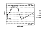
図2に蓄電モジュール101の電圧の使用下限電圧Vuse-udおよび使用上限電圧Vuse-upを概念図で示す。図3にn個の蓄電素子の電圧の動作保障下限電圧Vm-udおよび動作保障上限電圧Vm-upを概念図で示す。各概念図から理解されるように、蓄電モジュール101の電圧Vuse(Module_V)は、n個の蓄電素子の電圧の積算値に相当する。 FIG. 2 is a conceptual diagram showing the use lower limit voltage Vuse-ud and the use upper limit voltage Vuse-up of the voltage of the power storage module 101. FIG. 3 is a conceptual diagram showing the operation guarantee lower limit voltage Vm-ud and the operation guarantee upper limit voltage Vm-up of the voltages of n power storage elements. As understood from the conceptual diagrams, the voltage Vuse (Module_V) of the power storage module 101 corresponds to an integrated value of the voltages of n power storage elements.
n個の蓄電素子は、いずれも同じ動作保障下限電圧Vm-udおよび動作保障上限電圧Vm-upにより規制されている。しかし、実際には、n個の蓄電素子の性能は同じではない。そのため、従来のように、n個の蓄電素子の現在電圧を均等化すると、図4に示されるように、電圧の使用範囲の上下限でばらつきが生じる。例えば、いずれか1つの蓄電素子(蓄電素子Bmax)が動作保障上限電圧Vm-upに達した時点で、n個の全ての蓄電素子が同時に動作保障上限電圧Vm-upに達したものと見なされ、蓄電モジュール101の充電はストップされる。このとき、図5に示されるように、蓄電モジュール101の電圧Vuseは、蓄電素子Bmaxより低電圧な蓄電素子の影響により、Vuse-upより相当に低くなり得る。これにより、Vuse-ud以上かつVuse-up以下の電圧範囲が十分に活用されず、蓄電モジュール101はその性能を十分に発揮することができなくなる。 The n power storage elements are all regulated by the same operation guarantee lower limit voltage Vm-ud and operation guarantee upper limit voltage Vm-up. However, in practice, the performance of the n power storage elements is not the same. Therefore, when the current voltages of the n power storage elements are equalized as in the conventional case, as shown in FIG. 4, variations occur in the upper and lower limits of the voltage use range. For example, when any one of the storage elements (storage element Bmax) reaches the operation guarantee upper limit voltage Vm-up, it is considered that all n storage elements simultaneously reach the operation guarantee upper limit voltage Vm-up. The charging of the power storage module 101 is stopped. At this time, as shown in FIG. 5, the voltage Vuse of the power storage module 101 can be considerably lower than Vuse-up due to the influence of the power storage element having a voltage lower than that of the power storage element Bmax. As a result, a voltage range of Vuse-ud or more and Vuse-up or less is not fully utilized, and the power storage module 101 cannot sufficiently exhibit its performance.
一方、図6では、n個の蓄電素子が全てVm-upに至った時点で均等化が行われている。この場合、n個の蓄電素子の電圧をそれぞれ独立にVs(i)に設定した後、Vmまで充電することで、Vmで均等化が行われる。ただし、Vs(i)は、n個の蓄電素子がVmで均等化されるように、計算部14が算出する。これにより、図7に示されるように、蓄電モジュール101の電圧VuseをVuse-upまで上昇させることが可能となる。
On the other hand, in FIG. 6, equalization is performed when all n power storage elements reach Vm-up. In this case, the voltages of the n power storage elements are set to Vs (i) independently and then charged to Vm, whereby equalization is performed with Vm. However, Vs (i) is calculated by the
次に、本実施形態に係る電圧制御方法について、図8を参照しながら説明する。以下では、蓄電素子としてキャパシタを用いる場合について説明する。なお、図8のフローは一例に過ぎず、各工程の順序、工程数などは、図8および以下の説明に限定されるものではない。 Next, the voltage control method according to the present embodiment will be described with reference to FIG. Below, the case where a capacitor is used as an electrical storage element is demonstrated. Note that the flow in FIG. 8 is merely an example, and the order of the steps, the number of steps, and the like are not limited to those in FIG. 8 and the following description.
電圧制御方法のスタート時点は、特に限定されないが、例えば、電圧制御装置が起動されたときにスタートすればよい。電圧制御装置が起動されると、第2制御部12の第2電圧センサにより、各蓄電素子の現在電圧Vr(i)が測定される(S10)。測定されたVr(i)は、モジュール制御部102から通信手段104を通って演算処理装置103に送信される。
The starting point of the voltage control method is not particularly limited. For example, it may be started when the voltage control device is activated. When the voltage control device is activated, the current voltage Vr (i) of each power storage element is measured by the second voltage sensor of the second control unit 12 (S10). The measured Vr (i) is transmitted from the
一方、計算部14では、Vmの設定が行われる(S20)。Vmは、蓄電モジュール101の用途、使用方法などにより、適時に適切な値に設定する。なお、Vmの設定は任意で行えばよく、予め定められたVmを演算処理装置103のメモリユニット16から読み出すだけでもよい。
On the other hand, the
次に、n個の蓄電素子から、基準となる1つの蓄電素子B(base)が選定される(S11)。蓄電素子B(base)の選定基準は、特に限定されないが、例えばVmを動作保障上限電圧Vm-upに設定する場合には、現在電圧が最も低い蓄電素子を選定することが望ましい。この場合、通常は、蓄電素子B(base)以外の蓄電素子を放電させる操作で均等化処理を行うことができる。なお、蓄電素子B(base)の選定は、予め蓄電素子B(base)が定められていない場合、もしくは予め蓄電素子B(base)が定められているが、変更が必要となった場合にだけ行えばよい。 Next, one storage element B (base) serving as a reference is selected from the n storage elements (S11). The criteria for selecting the storage element B (base) are not particularly limited. For example, when Vm is set to the operation guarantee upper limit voltage Vm-up, it is desirable to select the storage element having the lowest current voltage. In this case, the equalization process can be normally performed by an operation of discharging power storage elements other than the power storage element B (base). The storage element B (base) is selected only when the storage element B (base) is not determined in advance or when the storage element B (base) is determined in advance but needs to be changed. Just do it.
次に、Vr(i)から蓄電量Qr(i)が算出される(S12)。キャパシタの場合、Vr(i)から現在のSOCと静電容量Cr(i)が導かれるため、Qr(i)=Cr(i)×Vr(i)により現在の蓄電量が算出される。電圧と静電容量との関係は予め測定し、演算処理装置103のメモリユニット16に格納しておけばよい。
Next, the charged amount Qr (i) is calculated from Vr (i) (S12). In the case of a capacitor, since the current SOC and capacitance Cr (i) are derived from Vr (i), the current charged amount is calculated by Qr (i) = Cr (i) × Vr (i). The relationship between the voltage and the capacitance may be measured in advance and stored in the
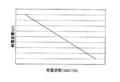
図9に、Cr(i)とSOCとの関係の一例を示す。Vr(i)とSOCは概ね比例関係にある。ただし、電圧と静電容量との関係は温度にも依存するため、蓄電モジュール101の使用環境温度範囲が広い場合には、図10に示すような、SOCと温度と静電容量との関係を示す換算テーブルを演算処理装置103のメモリユニット16に格納しておき、これを用いてVr(i)から蓄電量Qr(i)を算出することが望ましい。この場合、電圧制御装置100に、演算処理装置103と連絡し合うように、蓄電モジュール101の温度を測定する温度センサを設ければよい。
FIG. 9 shows an example of the relationship between Cr (i) and SOC. Vr (i) and SOC are approximately proportional. However, since the relationship between the voltage and the capacitance also depends on the temperature, when the operating environment temperature range of the power storage module 101 is wide, the relationship between the SOC, the temperature, and the capacitance as shown in FIG. It is desirable to store the conversion table shown in the
次に、n個の蓄電量Qr(i)の算出値から、蓄電素子B(base)以外の(n−1)個の蓄電素子と、蓄電素子B(base)との蓄電量の差ΔQr(i)を求める(S13)。 Next, from the calculated value of the n power storage amounts Qr (i), a difference ΔQr () between the power storage amounts of (n−1) power storage elements other than the power storage element B (base) and the power storage element B (base). i) is obtained (S13).
一方、上記と同様に、n個の蓄電素子B(i)のVmにおける蓄電量Qm(i)を算出する(S21)。Vmのときの蓄電素子のSOCと静電容量Cm(i)は、上記換算テーブルから求めることができる。Qm(i)=Cm(i)×Vmにより、Vmにおける蓄電量Qm(i)が算出される。そして、上記と同様に、n個の蓄電量Qm(i)の算出値から、蓄電素子B(base)以外の(n−1)個の蓄電素子と、蓄電素子B(base)との蓄電量の差ΔQm(i)を求める(S22)。なお、予めVmと蓄電素子B(base)が定められている場合には、ΔQm(i)についても予め算出し、演算処理装置103のメモリユニット16に格納しておくことができる。
On the other hand, similarly to the above, the storage amount Qm (i) at Vm of the n storage elements B (i) is calculated (S21). The SOC and the capacitance Cm (i) of the electricity storage element at Vm can be obtained from the conversion table. The amount of electricity stored Qm (i) at Vm is calculated by Qm (i) = Cm (i) × Vm. Then, similarly to the above, from the calculated value of the n power storage amount Qm (i), the power storage amount of (n−1) power storage elements other than the power storage device B (base) and the power storage device B (base) A difference ΔQm (i) is obtained (S22). If Vm and power storage element B (base) are determined in advance, ΔQm (i) can also be calculated in advance and stored in
次に、ΔQr(i)が、ΔQm(i)に近づくように、Vs(i)を計算する(S30)。Vs(i)は、蓄電素子B(base)以外の蓄電素子について、(n−1)個が算出される。蓄電素子B(base)のVs(i)は、現在電圧Vr(i)のままでよい。ただし、回路全体の消費電流を加味すると、時間経過とともにVr(i)は低くなる。これに伴ってVs(i)も低く設定してもよい。 Next, Vs (i) is calculated so that ΔQr (i) approaches ΔQm (i) (S30). Vs (i) is calculated for (n−1) power storage elements other than the power storage element B (base). Vs (i) of the storage element B (base) may remain at the current voltage Vr (i). However, when the current consumption of the entire circuit is taken into account, Vr (i) decreases with time. Accordingly, Vs (i) may be set low.
例えば、蓄電素子B(j)と蓄電素子B(base)との蓄電量の差ΔQr(j)が、ΔQm(j)より大きい場合、蓄電素子B(base)を放電させず、蓄電素子B(j)だけを一定時間放電させることで、ΔQr(j)はΔQm(j)に近づく。このとき、ΔQr(j)−ΔQm(j)=Δq(j)で表される電荷量、Δq(j)=Cr(j)×ΔVの関係式およびVs(j)=Vr(j)−ΔVの関係式から、Vs(j)を求めることができる。 For example, when the difference ΔQr (j) in the storage amount between the storage element B (j) and the storage element B (base) is greater than ΔQm (j), the storage element B (base) is not discharged and the storage element B ( By discharging only j) for a certain time, ΔQr (j) approaches ΔQm (j). At this time, a charge amount represented by ΔQr (j) −ΔQm (j) = Δq (j), a relational expression of Δq (j) = Cr (j) × ΔV, and Vs (j) = Vr (j) −ΔV From the relational expression, Vs (j) can be obtained.
ただし、回路全体の消費電流を加味して、時間経過とともにVs(j)を更新してもよく、事前に均等化に要する時間を推定し、その時間経過後のVs(j)を算出してもよい。そのときは、回路全体の消費電流が各蓄電素子を流れるという前提で、各蓄電素子の電圧降下を算出し、Vs(j)に反映させればよい。 However, Vs (j) may be updated with the passage of time in consideration of the current consumption of the entire circuit, the time required for equalization is estimated in advance, and Vs (j) after the lapse of time is calculated. Also good. At that time, the voltage drop of each power storage element may be calculated and reflected in Vs (j) on the assumption that the current consumption of the entire circuit flows through each power storage element.
回路全体の消費電流(以下、Ik)には、均等化のため消費電流(以下、I)、モジュール制御部102の動作および演算処理装置103の動作に必要な消費電流などが含まれる。時間経過とともにVs(j)を更新する場合には、均等化のための個別放電の開始後、一定時間Δt毎に、Ikから電荷量Δqk=Ik×Δtを求め、Δqk=Cr(j)×ΔVkの関係式と、Vs´(j)=Vs(j)−ΔVkの関係式とを用いて、更新されたVs´(j)を求めることができる。
The current consumption of the entire circuit (hereinafter referred to as Ik) includes current consumption for equalization (hereinafter referred to as I), current consumption necessary for the operation of the
均等化のため消費電流Iは、個別放電手段の消費電流であり、図1の場合、スイッチ制御部13によりスイッチS(j)だけをオン、他のスイッチをオフにしたときに構成される、蓄電素子B(j)、抵抗R(j)およびスイッチS(j)を含む回路(均等化放電回路)を流れる電流である。個別放電の開始前に均等化に要する時間を推定する場合、均等化放電回路の抵抗とVr(j)からIを算出し、Δq(j)=I×T(時間)の関係式から電流Iを流す時間Tを算出すればよい。次に、Ikが時間Tで使用する電荷量Δqk=Ik×Tを求め、Δqk=Cr(j)×ΔVkの関係式と、Vs"(j)=Vs(j)−ΔVkの関係式とを用いて、回路全体の消費電流を考慮したVs"(j)を推定することができる。
The current consumption I for equalization is the current consumption of the individual discharge means. In the case of FIG. 1, it is configured when only the switch S (j) is turned on and the other switches are turned off by the
次に、蓄電素子B(base)以外の蓄電素子の均等化のための充放電が行われる(S31)。均等化のための充放電とは、(n−1)個の蓄電素子B(i)を、それぞれに設定されたVs(i)まで充電または放電する処理である。 Next, charge / discharge for equalization of power storage elements other than the power storage element B (base) is performed (S31). Charge / discharge for equalization is a process of charging or discharging (n−1) power storage elements B (i) to Vs (i) set to each.
均等化充放電が行われると、その後、蓄電モジュール101の通常の充放電が行われたときに(S32)、n個の蓄電素子はほぼ同じタイミングでVmになり、Vmで電圧が均等化される。 When equalization charge / discharge is performed, after that, when normal charge / discharge of the power storage module 101 is performed (S32), the n power storage elements become Vm at almost the same timing, and the voltage is equalized by Vm. The
通常充放電では、所定時間ごとに、n個の蓄電素子B(i)の電圧Vr(i)が測定され、Vm-upと対比される(S33)。Vr(i)<Vm-upであれば(Y)、充電が継続され、次に、Vr(i)とVm-udとが対比される(S34)。Vr(i)>Vm-udであれば(Y)、放電が継続される。一方、S33でVr(i)≧Vm-upであれば(N)、充電中の場合には充電がストップされる。S34でVr(i)≦Vm-udであれば(N)、放電中の場合には放電がストップされる。全ての蓄電素子B(1)〜B(n)について同様の対比が行われる。よって、いずれか1つでもVr(i)≧Vm-upまたはVr(i)≦Vm-udであれば、充電中の場合には充電が、放電中の場合には放電がストップされる。このような制御は、第2制御部12により行われる。
In normal charging / discharging, the voltage Vr (i) of n power storage elements B (i) is measured every predetermined time and compared with Vm-up (S33). If Vr (i) <Vm-up (Y), charging is continued, and then Vr (i) and Vm-ud are compared (S34). If Vr (i)> Vm-ud (Y), the discharge is continued. On the other hand, if Vr (i) ≧ Vm-up (N) in S33, charging is stopped when charging is in progress. If Vr (i) ≦ Vm−ud in S34 (N), the discharge is stopped when discharging is in progress. The same comparison is performed for all the power storage elements B (1) to B (n). Therefore, if any one of them satisfies Vr (i) ≧ Vm-up or Vr (i) ≦ Vm-ud, charging is stopped during charging and discharging is stopped when discharging. Such control is performed by the
一方、第1制御部11は、所定時間ごとに、蓄電モジュール101の電圧Vuseを測定し、Vuse-upと対比する(S35)。Vuse<Vuse-upであれば(Y)、充電が継続され、次に、VuseとVuse-udとが対比される(S36)。Vuse>Vuse-udであれば(Y)、放電が継続される。Vuse≧Vuse-upまたはVuse≦Vuse-udであれば、充電中の場合には充電が、放電中の場合には放電がストップされる。
On the other hand, the
蓄電モジュールの使用を継続すると、徐々に蓄電素子の劣化が進行する。劣化の進行度合いは蓄電素子により相違する。よって、所定期間の蓄電モジュールの使用後、蓄電素子の電圧またはSOCと静電容量との相関関係(例えば上記換算テーブル)を補正して設定し直すリセットを行うことが望ましい。補正の方法は、特に制限されないが、キャパシタの場合、静電容量は、微小時間だけ電流を流したときのキャパシタの電圧変化(ΔV/I)から推測することができる。よって、適時に、相関関係を補正し、更新することができる。 When the use of the power storage module is continued, the power storage element gradually deteriorates. The degree of progress of deterioration differs depending on the storage element. Therefore, it is desirable to perform reset after correcting the correlation between the voltage of the power storage element or the SOC and the capacitance (for example, the conversion table) after using the power storage module for a predetermined period. The correction method is not particularly limited, but in the case of a capacitor, the electrostatic capacity can be estimated from the voltage change (ΔV / I) of the capacitor when a current is passed for a very short time. Therefore, the correlation can be corrected and updated in a timely manner.
蓄電素子の劣化が進行すると、その動作保障電圧範囲も変化する。よって、所定期間の蓄電モジュールの使用後には、蓄電モジュールのVuse-udおよびVuse-up、蓄電素子のVm-udおよびVm-up、並びにVmについても、補正して設定し直すリセットを行うことが望ましい。 As the deterioration of the storage element progresses, the guaranteed operating voltage range also changes. Therefore, after using the power storage module for a predetermined period, Vuse-ud and Vuse-up of the power storage module, Vm-ud and Vm-up of the power storage element, and Vm may be reset after being corrected and reset. desirable.
本発明の実施形態によれば、蓄電モジュールが本来備える容量を、より有効に活用することができる。 According to the embodiment of the present invention, the capacity originally provided in the power storage module can be utilized more effectively.
100:電圧制御装置、101:蓄電モジュール、102:モジュール制御部、103:演算処理装置、104:通信手段、11:第1制御部、12:第2制御部、13:SW制御部、14:計算部、15:充放電制御部、16:メモリ 100: voltage control device, 101: power storage module, 102: module control unit, 103: arithmetic processing unit, 104: communication means, 11: first control unit, 12: second control unit, 13: SW control unit, 14: Calculation unit, 15: charge / discharge control unit, 16: memory
Claims (10)
前記蓄電モジュールの電圧を使用下限電圧Vuse-ud以上、使用上限電圧Vuse-up以下に制御する第1制御部と、
前記n個の蓄電素子B(i)の電圧をそれぞれ個別に動作保障下限電圧Vm-ud以上、動作保障上限電圧Vm-up以下に制御する第2制御部と、
均等化目標電圧Vm(ただし、Vm-ud≦Vm≦Vm-up)に基づいて、前記n個の蓄電素子B(i)の設定電圧Vs(i)(ただし、Vm≠Vs(i))をそれぞれ個別に求める計算部と、
前記Vs(i)に向けて、前記n個の蓄電素子B(i)の少なくとも一部をそれぞれ個別に充電または放電する充放電制御部と、を具備し、
前記計算部は、前記n個の蓄電素子B(i)が前記Vmで均等化されるように前記Vs(i)を算出する、蓄電モジュールの電圧制御装置。 A power storage module including n (2 ≦ n) power storage elements B (i) (i is an integer from 1 to n) connected in series;
A first control unit for controlling the voltage of the power storage module to be not less than the use lower limit voltage Vuse-ud and not more than the use upper limit voltage Vuse-up;
A second controller for individually controlling the voltages of the n power storage elements B (i) to be not less than the operation guarantee lower limit voltage Vm-ud and not more than the operation guarantee upper limit voltage Vm-up;
Based on the equalization target voltage Vm (where Vm−ud ≦ Vm ≦ Vm−up), the set voltage Vs (i) (where Vm ≠ Vs (i)) of the n power storage elements B (i) A calculation part to be obtained individually,
A charge / discharge control unit that individually charges or discharges at least a part of the n power storage elements B (i) toward the Vs (i),
The voltage calculation device for a power storage module, wherein the calculation unit calculates the Vs (i) so that the n power storage elements B (i) are equalized with the Vm.
前記n個の蓄電素子B(i)の現在電圧Vr(i)における蓄電量の差ΔQrが、前記均等化目標電圧Vmにおける蓄電量の差ΔQmに近づくように、前記Vs(i)を算出する、請求項1に記載の蓄電モジュールの電圧制御装置。 The calculator is
The Vs (i) is calculated so that the difference ΔQr in the storage amount at the current voltage Vr (i) of the n storage elements B (i) approaches the difference ΔQm in the storage amount at the equalization target voltage Vm. The voltage control device for a power storage module according to claim 1.
前記n個の蓄電素子B(i)の電圧または充電状態と、静電容量と、の相関関係を利用して、前記ΔQrおよび前記ΔQmを算出する、請求項3に記載の蓄電モジュールの電圧制御装置。 The calculator is
The voltage control of the power storage module according to claim 3, wherein ΔQr and ΔQm are calculated using a correlation between a voltage or a charged state of the n power storage elements B (i) and a capacitance. apparatus.
(II)前記n個の蓄電素子B(i)の電圧をそれぞれ個別に動作保障下限電圧Vm-ud以上、動作保障上限電圧Vm-up以下に制御する工程と、
(III)均等化目標電圧Vm(ただし、Vm-ud≦Vm≦Vm-up)に基づいて、前記n個の蓄電素子B(i)の設定電圧Vs(i)(ただし、Vm≠Vs(i))をそれぞれ個別に求める工程と、
(IV)前記Vs(i)に向けて、前記n個の蓄電素子B(i)の少なくとも一部をそれぞれ個別に充電または放電する工程と、を具備し、
前記Vs(i)は、前記n個の蓄電素子B(i)が前記Vmで均等化されるように算出される、蓄電モジュールの電圧制御方法。 (I) The voltage of a power storage module including n (2 ≦ n) power storage elements B (i) (i is an integer from 1 to n) connected in series is equal to or higher than the use lower limit voltage Vuse-ud and the use upper limit voltage. A process of controlling to below Vuse-up;
(II) controlling the voltages of the n power storage elements B (i) individually to be not less than the operation guarantee lower limit voltage Vm-ud and not more than the operation guarantee upper limit voltage Vm-up;
(III) Based on the equalization target voltage Vm (where Vm−ud ≦ Vm ≦ Vm−up), the set voltage Vs (i) of the n power storage elements B (i) (where Vm ≠ Vs (i )) For each process,
(IV) charging or discharging each of at least a part of the n power storage elements B (i) toward Vs (i),
The voltage control method for the power storage module, wherein the Vs (i) is calculated so that the n power storage elements B (i) are equalized with the Vm.
前記n個の蓄電素子B(i)の前記Vmにおける蓄電量の差ΔQmを計算する工程と、
前記n個の蓄電素子B(i)の現在電圧Vr(i)をそれぞれ測定し、前記n個の蓄電素子B(i)の前記Vr(i)における蓄電量の差ΔQrを計算する工程と、
前記ΔQrが、前記ΔQmに近づくように、前記Vs(i)を算出する工程と、を具備する、請求項5に記載の蓄電モジュールの電圧制御方法。 The step (III)
Calculating a difference ΔQm in the amount of electricity stored in the Vm of the n power storage elements B (i);
Measuring a current voltage Vr (i) of each of the n power storage elements B (i), and calculating a storage amount difference ΔQr in the Vr (i) of the n power storage elements B (i);
The voltage control method for a power storage module according to claim 5, further comprising: calculating the Vs (i) so that the ΔQr approaches the ΔQm.
前記n個の蓄電素子B(i)の電圧または充電状態と、静電容量と、の相関関係を利用して、前記ΔQrおよび前記ΔQmを算出する工程を含む、請求項7に記載の蓄電モジュールの電圧制御方法。 The step (III)
The power storage module according to claim 7, comprising a step of calculating the ΔQr and the ΔQm using a correlation between a voltage or a charged state of the n power storage elements B (i) and a capacitance. Voltage control method.
The voltage control method for a power storage module according to claim 9, further comprising a step of resetting the Vm in accordance with a deterioration state of the n power storage elements B (i).
Priority Applications (1)
| Application Number | Priority Date | Filing Date | Title |
|---|---|---|---|
| JP2015104545A JP2016220445A (en) | 2015-05-22 | 2015-05-22 | Voltage control device for power storage module, and voltage control method |
Applications Claiming Priority (1)
| Application Number | Priority Date | Filing Date | Title |
|---|---|---|---|
| JP2015104545A JP2016220445A (en) | 2015-05-22 | 2015-05-22 | Voltage control device for power storage module, and voltage control method |
Publications (1)
| Publication Number | Publication Date |
|---|---|
| JP2016220445A true JP2016220445A (en) | 2016-12-22 |
Family
ID=57578780
Family Applications (1)
| Application Number | Title | Priority Date | Filing Date |
|---|---|---|---|
| JP2015104545A Pending JP2016220445A (en) | 2015-05-22 | 2015-05-22 | Voltage control device for power storage module, and voltage control method |
Country Status (1)
| Country | Link |
|---|---|
| JP (1) | JP2016220445A (en) |
Cited By (1)
| Publication number | Priority date | Publication date | Assignee | Title |
|---|---|---|---|---|
| WO2024028955A1 (en) * | 2022-08-01 | 2024-02-08 | ビークルエナジージャパン株式会社 | Battery control method, battery control device, and vehicle control method |
Citations (3)
| Publication number | Priority date | Publication date | Assignee | Title |
|---|---|---|---|---|
| JP2000324712A (en) * | 1999-03-09 | 2000-11-24 | Asahi Glass Co Ltd | Electric double-layer capacitor device and voltage control method therefor |
| JP2009232659A (en) * | 2008-03-25 | 2009-10-08 | Mazda Motor Corp | Charge-discharge control method and charge-discharge control device of battery |
| WO2012143996A1 (en) * | 2011-04-18 | 2012-10-26 | 日立ビークルエナジー株式会社 | Electric storage device |
-
2015
- 2015-05-22 JP JP2015104545A patent/JP2016220445A/en active Pending
Patent Citations (3)
| Publication number | Priority date | Publication date | Assignee | Title |
|---|---|---|---|---|
| JP2000324712A (en) * | 1999-03-09 | 2000-11-24 | Asahi Glass Co Ltd | Electric double-layer capacitor device and voltage control method therefor |
| JP2009232659A (en) * | 2008-03-25 | 2009-10-08 | Mazda Motor Corp | Charge-discharge control method and charge-discharge control device of battery |
| WO2012143996A1 (en) * | 2011-04-18 | 2012-10-26 | 日立ビークルエナジー株式会社 | Electric storage device |
Cited By (1)
| Publication number | Priority date | Publication date | Assignee | Title |
|---|---|---|---|---|
| WO2024028955A1 (en) * | 2022-08-01 | 2024-02-08 | ビークルエナジージャパン株式会社 | Battery control method, battery control device, and vehicle control method |
Similar Documents
| Publication | Publication Date | Title |
|---|---|---|
| JP6791386B2 (en) | Charging time calculation method and charging control device | |
| US9438059B2 (en) | Battery control apparatus and battery control method | |
| CN103872398B (en) | Charging method of rechargeable battery and related charging structure | |
| KR101956088B1 (en) | State controlling apparatus, equalization of electrical storage device | |
| US20130057224A1 (en) | Control system of battery pack and method of charging and discharging using the same | |
| KR101084828B1 (en) | Battery pack and Charging Control Method for Battery Pack | |
| KR101702824B1 (en) | Electricity storage element charging method and electricity storage device | |
| JP6648709B2 (en) | Battery module controller | |
| WO2015178075A1 (en) | Battery control device | |
| JP6041040B2 (en) | Storage battery, storage battery control method, control device, and control method | |
| JP5482809B2 (en) | Equalization equipment | |
| JP2014068468A (en) | Charge control device | |
| US10355510B2 (en) | Battery charging method and battery pack using the same | |
| KR102349705B1 (en) | Battery cell balancing circuit and apparatus and method for balancing of a battery cell for using the same | |
| WO2015133401A1 (en) | Control unit, storage battery system, battery cell balancing method, and program | |
| JP5165405B2 (en) | Charge control circuit, battery pack, and charging system | |
| KR101954285B1 (en) | State controlling apparatus, equalization of electrical storage device | |
| WO2018089519A1 (en) | Real time active multi-cell balancing | |
| JP2015195653A (en) | Battery system, charging/discharging control program, and charging/discharging control method | |
| KR102082382B1 (en) | Multi battery pack apparatus and control method for charging the same | |
| JP2016220445A (en) | Voltage control device for power storage module, and voltage control method | |
| JP2008060032A (en) | Battery pack, and detecting method | |
| JP2017198455A (en) | Charge rate estimating device | |
| CN110622385B (en) | Charging of a battery | |
| JP6172148B2 (en) | Battery control device, power storage device, operation method of power storage device, and program |
Legal Events
| Date | Code | Title | Description |
|---|---|---|---|
| A621 | Written request for application examination |
Free format text: JAPANESE INTERMEDIATE CODE: A621 Effective date: 20171221 |
|
| A977 | Report on retrieval |
Free format text: JAPANESE INTERMEDIATE CODE: A971007 Effective date: 20180928 |
|
| A131 | Notification of reasons for refusal |
Free format text: JAPANESE INTERMEDIATE CODE: A131 Effective date: 20181009 |
|
| A521 | Request for written amendment filed |
Free format text: JAPANESE INTERMEDIATE CODE: A523 Effective date: 20181102 |
|
| RD02 | Notification of acceptance of power of attorney |
Free format text: JAPANESE INTERMEDIATE CODE: A7422 Effective date: 20181102 |
|
| A02 | Decision of refusal |
Free format text: JAPANESE INTERMEDIATE CODE: A02 Effective date: 20181218 |