JP2016212941A - METHODS OF MAKING MgO BARRIER LAYER FOR TMR SENSOR - Google Patents
METHODS OF MAKING MgO BARRIER LAYER FOR TMR SENSOR Download PDFInfo
- Publication number
- JP2016212941A JP2016212941A JP2015242007A JP2015242007A JP2016212941A JP 2016212941 A JP2016212941 A JP 2016212941A JP 2015242007 A JP2015242007 A JP 2015242007A JP 2015242007 A JP2015242007 A JP 2015242007A JP 2016212941 A JP2016212941 A JP 2016212941A
- Authority
- JP
- Japan
- Prior art keywords
- layer
- depositing
- mgo
- chamber
- target
- Prior art date
- Legal status (The legal status is an assumption and is not a legal conclusion. Google has not performed a legal analysis and makes no representation as to the accuracy of the status listed.)
- Pending
Links
Images


Classifications
-
- C—CHEMISTRY; METALLURGY
- C23—COATING METALLIC MATERIAL; COATING MATERIAL WITH METALLIC MATERIAL; CHEMICAL SURFACE TREATMENT; DIFFUSION TREATMENT OF METALLIC MATERIAL; COATING BY VACUUM EVAPORATION, BY SPUTTERING, BY ION IMPLANTATION OR BY CHEMICAL VAPOUR DEPOSITION, IN GENERAL; INHIBITING CORROSION OF METALLIC MATERIAL OR INCRUSTATION IN GENERAL
- C23C—COATING METALLIC MATERIAL; COATING MATERIAL WITH METALLIC MATERIAL; SURFACE TREATMENT OF METALLIC MATERIAL BY DIFFUSION INTO THE SURFACE, BY CHEMICAL CONVERSION OR SUBSTITUTION; COATING BY VACUUM EVAPORATION, BY SPUTTERING, BY ION IMPLANTATION OR BY CHEMICAL VAPOUR DEPOSITION, IN GENERAL
- C23C14/00—Coating by vacuum evaporation, by sputtering or by ion implantation of the coating forming material
- C23C14/06—Coating by vacuum evaporation, by sputtering or by ion implantation of the coating forming material characterised by the coating material
- C23C14/08—Oxides
- C23C14/081—Oxides of aluminium, magnesium or beryllium
-
- C—CHEMISTRY; METALLURGY
- C23—COATING METALLIC MATERIAL; COATING MATERIAL WITH METALLIC MATERIAL; CHEMICAL SURFACE TREATMENT; DIFFUSION TREATMENT OF METALLIC MATERIAL; COATING BY VACUUM EVAPORATION, BY SPUTTERING, BY ION IMPLANTATION OR BY CHEMICAL VAPOUR DEPOSITION, IN GENERAL; INHIBITING CORROSION OF METALLIC MATERIAL OR INCRUSTATION IN GENERAL
- C23C—COATING METALLIC MATERIAL; COATING MATERIAL WITH METALLIC MATERIAL; SURFACE TREATMENT OF METALLIC MATERIAL BY DIFFUSION INTO THE SURFACE, BY CHEMICAL CONVERSION OR SUBSTITUTION; COATING BY VACUUM EVAPORATION, BY SPUTTERING, BY ION IMPLANTATION OR BY CHEMICAL VAPOUR DEPOSITION, IN GENERAL
- C23C14/00—Coating by vacuum evaporation, by sputtering or by ion implantation of the coating forming material
- C23C14/22—Coating by vacuum evaporation, by sputtering or by ion implantation of the coating forming material characterised by the process of coating
- C23C14/34—Sputtering
- C23C14/3464—Sputtering using more than one target
-
- C—CHEMISTRY; METALLURGY
- C23—COATING METALLIC MATERIAL; COATING MATERIAL WITH METALLIC MATERIAL; CHEMICAL SURFACE TREATMENT; DIFFUSION TREATMENT OF METALLIC MATERIAL; COATING BY VACUUM EVAPORATION, BY SPUTTERING, BY ION IMPLANTATION OR BY CHEMICAL VAPOUR DEPOSITION, IN GENERAL; INHIBITING CORROSION OF METALLIC MATERIAL OR INCRUSTATION IN GENERAL
- C23C—COATING METALLIC MATERIAL; COATING MATERIAL WITH METALLIC MATERIAL; SURFACE TREATMENT OF METALLIC MATERIAL BY DIFFUSION INTO THE SURFACE, BY CHEMICAL CONVERSION OR SUBSTITUTION; COATING BY VACUUM EVAPORATION, BY SPUTTERING, BY ION IMPLANTATION OR BY CHEMICAL VAPOUR DEPOSITION, IN GENERAL
- C23C14/00—Coating by vacuum evaporation, by sputtering or by ion implantation of the coating forming material
- C23C14/22—Coating by vacuum evaporation, by sputtering or by ion implantation of the coating forming material characterised by the process of coating
- C23C14/56—Apparatus specially adapted for continuous coating; Arrangements for maintaining the vacuum, e.g. vacuum locks
- C23C14/568—Transferring the substrates through a series of coating stations
-
- C—CHEMISTRY; METALLURGY
- C23—COATING METALLIC MATERIAL; COATING MATERIAL WITH METALLIC MATERIAL; CHEMICAL SURFACE TREATMENT; DIFFUSION TREATMENT OF METALLIC MATERIAL; COATING BY VACUUM EVAPORATION, BY SPUTTERING, BY ION IMPLANTATION OR BY CHEMICAL VAPOUR DEPOSITION, IN GENERAL; INHIBITING CORROSION OF METALLIC MATERIAL OR INCRUSTATION IN GENERAL
- C23C—COATING METALLIC MATERIAL; COATING MATERIAL WITH METALLIC MATERIAL; SURFACE TREATMENT OF METALLIC MATERIAL BY DIFFUSION INTO THE SURFACE, BY CHEMICAL CONVERSION OR SUBSTITUTION; COATING BY VACUUM EVAPORATION, BY SPUTTERING, BY ION IMPLANTATION OR BY CHEMICAL VAPOUR DEPOSITION, IN GENERAL
- C23C14/00—Coating by vacuum evaporation, by sputtering or by ion implantation of the coating forming material
- C23C14/58—After-treatment
- C23C14/5806—Thermal treatment
-
- C—CHEMISTRY; METALLURGY
- C23—COATING METALLIC MATERIAL; COATING MATERIAL WITH METALLIC MATERIAL; CHEMICAL SURFACE TREATMENT; DIFFUSION TREATMENT OF METALLIC MATERIAL; COATING BY VACUUM EVAPORATION, BY SPUTTERING, BY ION IMPLANTATION OR BY CHEMICAL VAPOUR DEPOSITION, IN GENERAL; INHIBITING CORROSION OF METALLIC MATERIAL OR INCRUSTATION IN GENERAL
- C23C—COATING METALLIC MATERIAL; COATING MATERIAL WITH METALLIC MATERIAL; SURFACE TREATMENT OF METALLIC MATERIAL BY DIFFUSION INTO THE SURFACE, BY CHEMICAL CONVERSION OR SUBSTITUTION; COATING BY VACUUM EVAPORATION, BY SPUTTERING, BY ION IMPLANTATION OR BY CHEMICAL VAPOUR DEPOSITION, IN GENERAL
- C23C28/00—Coating for obtaining at least two superposed coatings either by methods not provided for in a single one of groups C23C2/00 - C23C26/00 or by combinations of methods provided for in subclasses C23C and C25C or C25D
- C23C28/30—Coatings combining at least one metallic layer and at least one inorganic non-metallic layer
- C23C28/32—Coatings combining at least one metallic layer and at least one inorganic non-metallic layer including at least one pure metallic layer
- C23C28/322—Coatings combining at least one metallic layer and at least one inorganic non-metallic layer including at least one pure metallic layer only coatings of metal elements only
-
- C—CHEMISTRY; METALLURGY
- C23—COATING METALLIC MATERIAL; COATING MATERIAL WITH METALLIC MATERIAL; CHEMICAL SURFACE TREATMENT; DIFFUSION TREATMENT OF METALLIC MATERIAL; COATING BY VACUUM EVAPORATION, BY SPUTTERING, BY ION IMPLANTATION OR BY CHEMICAL VAPOUR DEPOSITION, IN GENERAL; INHIBITING CORROSION OF METALLIC MATERIAL OR INCRUSTATION IN GENERAL
- C23C—COATING METALLIC MATERIAL; COATING MATERIAL WITH METALLIC MATERIAL; SURFACE TREATMENT OF METALLIC MATERIAL BY DIFFUSION INTO THE SURFACE, BY CHEMICAL CONVERSION OR SUBSTITUTION; COATING BY VACUUM EVAPORATION, BY SPUTTERING, BY ION IMPLANTATION OR BY CHEMICAL VAPOUR DEPOSITION, IN GENERAL
- C23C28/00—Coating for obtaining at least two superposed coatings either by methods not provided for in a single one of groups C23C2/00 - C23C26/00 or by combinations of methods provided for in subclasses C23C and C25C or C25D
- C23C28/30—Coatings combining at least one metallic layer and at least one inorganic non-metallic layer
- C23C28/34—Coatings combining at least one metallic layer and at least one inorganic non-metallic layer including at least one inorganic non-metallic material layer, e.g. metal carbide, nitride, boride, silicide layer and their mixtures, enamels, phosphates and sulphates
- C23C28/345—Coatings combining at least one metallic layer and at least one inorganic non-metallic layer including at least one inorganic non-metallic material layer, e.g. metal carbide, nitride, boride, silicide layer and their mixtures, enamels, phosphates and sulphates with at least one oxide layer
-
- G—PHYSICS
- G11—INFORMATION STORAGE
- G11B—INFORMATION STORAGE BASED ON RELATIVE MOVEMENT BETWEEN RECORD CARRIER AND TRANSDUCER
- G11B5/00—Recording by magnetisation or demagnetisation of a record carrier; Reproducing by magnetic means; Record carriers therefor
- G11B5/127—Structure or manufacture of heads, e.g. inductive
- G11B5/33—Structure or manufacture of flux-sensitive heads, i.e. for reproduction only; Combination of such heads with means for recording or erasing only
- G11B5/39—Structure or manufacture of flux-sensitive heads, i.e. for reproduction only; Combination of such heads with means for recording or erasing only using magneto-resistive devices or effects
- G11B5/3903—Structure or manufacture of flux-sensitive heads, i.e. for reproduction only; Combination of such heads with means for recording or erasing only using magneto-resistive devices or effects using magnetic thin film layers or their effects, the films being part of integrated structures
- G11B5/3906—Details related to the use of magnetic thin film layers or to their effects
- G11B5/3909—Arrangements using a magnetic tunnel junction
-
- B—PERFORMING OPERATIONS; TRANSPORTING
- B82—NANOTECHNOLOGY
- B82Y—SPECIFIC USES OR APPLICATIONS OF NANOSTRUCTURES; MEASUREMENT OR ANALYSIS OF NANOSTRUCTURES; MANUFACTURE OR TREATMENT OF NANOSTRUCTURES
- B82Y25/00—Nanomagnetism, e.g. magnetoimpedance, anisotropic magnetoresistance, giant magnetoresistance or tunneling magnetoresistance
-
- G—PHYSICS
- G11—INFORMATION STORAGE
- G11B—INFORMATION STORAGE BASED ON RELATIVE MOVEMENT BETWEEN RECORD CARRIER AND TRANSDUCER
- G11B5/00—Recording by magnetisation or demagnetisation of a record carrier; Reproducing by magnetic means; Record carriers therefor
- G11B5/127—Structure or manufacture of heads, e.g. inductive
- G11B5/31—Structure or manufacture of heads, e.g. inductive using thin films
- G11B5/3163—Fabrication methods or processes specially adapted for a particular head structure, e.g. using base layers for electroplating, using functional layers for masking, using energy or particle beams for shaping the structure or modifying the properties of the basic layers
Abstract
Description
背景
酸化マグネシウム(MgO)バリア層を有するトンネル磁気抵抗(TMR:tunneling magnetoresistive)センサは、高いTMR値および低い面積抵抗(RA)も提供するシンプルかつ堅牢なバリア層により、多くの商業用ディスクドライブ製品において読取機として使用されている。
Background Tunneling magnetoresistive (TMR) sensors with a magnesium oxide (MgO) barrier layer are used in many commercial disk drive products due to the simple and robust barrier layer that also provides high TMR and low area resistance (RA). Used as a reader.
ドライブ容量の増加についての要求が大きくなるにつれて、低いRAを維持しつつ読取機センサのTMRを増加する必要性があるが、これは大きな困難となっている。 As demand for increased drive capacity increases, there is a need to increase the TMR of the reader sensor while maintaining a low RA, which is a major challenge.
概要
本願明細書において記載される1つの特定の実現例は、TMRセンサのためのMgOバリア層を作製する方法であって、上記方法は、Mgターゲットから第1のMgO源層を堆積するステップと、酸素の存在下において反応性酸化物堆積プロセスを使用して、Mgターゲットから第1の層上に第2のMgO源層を堆積するステップと、Mgターゲットから第2の層上に第3のMgO源層を堆積するステップと、MgOバリア層を形成するよう、第1のMgO源層、第2のMgO源層および第3のMgO源層をアニールするステップとを含む。
SUMMARY One specific implementation described herein is a method of making a MgO barrier layer for a TMR sensor, the method comprising depositing a first MgO source layer from a Mg target; Depositing a second MgO source layer on the first layer from the Mg target using a reactive oxide deposition process in the presence of oxygen; and a third on the second layer from the Mg target. Depositing a MgO source layer and annealing the first MgO source layer, the second MgO source layer, and the third MgO source layer to form an MgO barrier layer.
別の特定の実現例は、TMRセンサのためのMgOバリア層を作製する方法であって、上記方法は、第1のチャンバにおいて第1のMg層を堆積するステップと、第1のチャンバまたは第1のチャンバとは異なる第2のチャンバにおいて、酸素の存在下で、反応性酸化物堆積プロセスを使用して第1のMg層上に第2のMg層を堆積するステップと、第1のチャンバ、第2のチャンバ、または第1のチャンバおよび第2のチャンバの両方とは異なる第3のチャンバのいずれかにおいて、第2のMgO層上に第3のMg層を堆積するステップと、MgOバリア層を形成するよう第1の層、第2の層および第3の層をアニールするステップとを含む。 Another particular implementation is a method of making a MgO barrier layer for a TMR sensor, the method comprising depositing a first Mg layer in a first chamber and a first chamber or second Depositing a second Mg layer on the first Mg layer using a reactive oxide deposition process in the presence of oxygen in a second chamber different from the first chamber; Depositing a third Mg layer on the second MgO layer in either the second chamber or a third chamber different from both the first chamber and the second chamber; and an MgO barrier Annealing the first layer, the second layer, and the third layer to form a layer.
この概要は、詳細な説明においてさらに以下に記載される概念のセレクションを簡素化された形態で紹介するために提供される。この概要は、特許請求される主題の主な特徴または必須の特徴を識別するようには意図されておらず、特許請求される主題の範囲を限定するために使用されることも意図されていない。これらおよびさまざまな他の特徴および利点は、以下の詳細な説明を読むことで明らかになるであろう。 This summary is provided to introduce a selection of concepts in a simplified form that are further described below in the detailed description. This summary is not intended to identify key features or essential features of the claimed subject matter, nor is it intended to be used to limit the scope of the claimed subject matter. . These and various other features and advantages will become apparent upon reading the following detailed description.
記載される技術は、添付の図面に関連して解釈されるさまざまな実現例を記載する以下の詳細な説明から最もよく理解される。 The described technology is best understood from the following detailed description, which sets forth various implementations that are to be interpreted in conjunction with the accompanying drawings.
詳細な説明
上に示されるように、特にMgOバリア層が存在する場合、低いRA(たとえば<0.7Ωμm2)を維持しつつ読取機センサのTMRを増加させることは困難であった。
DETAILED DESCRIPTION As indicated above, it was difficult to increase the TMR of the reader sensor while maintaining a low RA (eg, <0.7 Ωμm 2 ), especially when an MgO barrier layer is present.
無線周波数(RF)堆積プロセスがMgOバリア層を形成するために使用される場合、プラズマイオンがRF−MgOバリア層にダメージを与え、これがバリアの貧弱なバリアテクスチャ構造およびバリアにおけるピンホールにつながり、これらのすべてがTMRの低減および低いRAでの自由層との交換結合の増加(所望でない)につながる。増加した面積密度を得る1つの方法は、MgOバリア層の品質を向上させることである。本開示は、MgOバリア層を形成するために代替的なプロセスを使用することによってイオンダメージの問題へのソリューションを提供する。 When a radio frequency (RF) deposition process is used to form the MgO barrier layer, plasma ions can damage the RF-MgO barrier layer, leading to poor barrier texture structure of the barrier and pinholes in the barrier, All of these lead to reduced TMR and increased exchange coupling with the free layer at low RA (not desired). One way to obtain increased area density is to improve the quality of the MgO barrier layer. The present disclosure provides a solution to the problem of ionic damage by using an alternative process to form the MgO barrier layer.
バリア堆積のためにRF堆積プロセスおよびMgO酸化物ターゲットを使用する代わりに、本開示は、MgOバリア層の少なくとも一部を形成するために反応性酸化(R−ox:reactive oxidation)MgO堆積プロセスの使用を記載しており、これは、酸素ガスのような酸素の存在下でMg金属膜を堆積することにより行われる。そのようなR−ox MgOプロセスは、Mg金属膜の低パワーの堆積(たとえば600W未満または200W未満)で行われ、堆積された膜に対してイオンダメージをほとんどまたはまったく作り出さず、特に低いRAでのMgOバリア層の自由層交換結合を低減するとともにセンサのTMRを増加させる能力を有する。さらに、R−ox堆積プロセスによって形成されたMgOバリア層は、RF−MgOバリア層よりも均一かつ平滑であり、ピンホールが少ない。 Instead of using an RF deposition process and an MgO oxide target for barrier deposition, the present disclosure provides for a reactive oxidation (R-ox) MgO deposition process to form at least a portion of an MgO barrier layer. This is described by depositing a Mg metal film in the presence of oxygen, such as oxygen gas. Such R-ox MgO processes are performed with low power deposition (eg, less than 600 W or less than 200 W) of Mg metal films and produce little or no ion damage to the deposited films, especially at low RA. The ability to reduce the free layer exchange coupling of the MgO barrier layer and increase the TMR of the sensor. Furthermore, the MgO barrier layer formed by the R-ox deposition process is more uniform and smoother than the RF-MgO barrier layer and has fewer pinholes.
以下の記載において、本願明細書の一部を形成するとともに少なくとも1つの特定の実現例が例示により示される添付の図面が参照される。以下の記載は、付加的な特定の実現例を提供する。本開示の範囲または精神から逸脱することがなければ、他の実現例が考えられかつ作製されてもよいということが理解されるべきである。以下の詳細な説明はしたがって、限定的な意味で解釈されるべきではない。本開示はそのようには限定されず、当該開示のさまざまな局面の理解は、以下に提供される例の議論を通じて得られるであろう。 In the following description, reference is made to the accompanying drawings, which form a part hereof, and in which at least one specific implementation is shown by way of example. The following description provides additional specific implementations. It should be understood that other implementations may be envisaged and made without departing from the scope or spirit of the present disclosure. The following detailed description is, therefore, not to be construed in a limiting sense. The present disclosure is not so limited, and an understanding of various aspects of the disclosure will be gained through a discussion of the examples provided below.
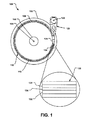
図1は、例示的なデータストレージシステム100、特定的にはディスクドライブ100の斜視図を示す。ディスクドライブ100は、1つ以上の回転可能な磁気データストレージ媒体またはディスク102が位置する筐体101を形成するよう結合する基部およびトップカバーを含む。ディスク102は、動作の間にスピンドル中心またはディスク回転軸104の周りを回転する。ディスク102は内径106および外径108を含んでおり、その間には円形の破線によって示される多くの同心のデータトラック110が存在する。データトラック110は、実質的に円形であり、ディスク102上においてドットまたは楕円として示される規則的に間隔が置かれたビット112から構成される。しかしながら、記載される技術は、連続的な磁気媒体、ディスクリートトラック(DT:discrete track)媒体などを含む他のタイプのストレージ媒体とともに使用され得るということが理解されるべきである。
FIG. 1 shows a perspective view of an exemplary
異なるデータトラック110においてディスク102上のビット112に情報が書き込まれるとともに情報がビット112から読み出され得る。アクチュエータ回転軸122を有するヘッドジンバルアセンブリ(HGA)120は、ディスク動作の間にディスク102の表面の上に近接近して、スライダ124をアーム126上に支持する。複数のディスク102のパックが利用される場合、各ディスク102または媒体表面は、その対応するディスク102に隣接および連通して搭載される関連付けられるスライダ124を有する。
Information can be written to and read from
ディスク102に最も近くかつ反対側のスライダ124の表面は、空気軸受面(ABS:air-bearing surface)と呼ばれる。使用時には、シーク動作の間、ヘッドジンバルアセンブリ120は、アクチュエータ回転軸122の周りを回転して、データトラック110の対象データトラックの上にスライダ124およびヘッドジンバルアセンブリ120を位置決めする。ディスク102がスピンすると、スライダ124とディスク102の表面との間に空気の層が形成され、スライダ124がディスク102の上を「飛ぶ」ことになる。その後、スライダ124上のトランスデューサが、対象データトラック110においてビット112からデータを読み出すまたは書き込む。
The surface of the
図1の差し込み図は、ABSから見たトランスデューサ130、特にトンネル磁気抵抗(TMR)センサの例示的な実現例の部分を示す。トランスデューサ130またはセンサ130は、ピン基準層132と自由層134とを含む複数の強磁性層と、その間の非磁性の誘電性MgO(酸化マグネシウム)バリア層136とによって形成される。MgOバリア層136は、部分的に反応性酸化堆積プロセスを利用して形成された。
The inset of FIG. 1 shows a portion of an exemplary implementation of a
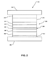
図2を参照して、TMRセンサ200は、薄い非磁性誘電体層によって分離される強磁性層を有する層の積層体として示される。
Referring to FIG. 2,
TMRセンサ200における底(シード)層202は、層を重ねる際に平滑かつ稠密な結晶成長を促進する1つ以上のシード層から一般に形成される。シード層202の上および随意には隣接しているのは、反強磁性(AFM:antiferromagnetic)ピン層204および合成反強磁性(SAF:synthetic antiferromagnetic)構造206であり、合成反強磁性構造206は、強磁性ピン層208と、非磁性スペーサ層(たとえばRuスペーサ層)210と、基準層212とから構成され、AFM層204上に存在する。特にMgOバリア層であるトンネルバリア層214は、SAF構造206の上、特に基準層212の上に位置決めされる。強磁性の「自由」層216は、MgOバリア層214上に形成される。TMRセンサ200の頂部にはキャップ層218が存在する。
The bottom (seed)
SAF構造206は、隣接するAFM層204との交換結合によって固定される。自由層216は、基準層212における磁気モーメントに平行または逆平行であるとともに外部磁界に応答してスイッチングする磁気モーメントを有する。MgOバリア層214は、伝導電子の量子力学的トンネリング(quantum mechanical tunneling)によって電流がそれを通過し得るほど十分に薄い。バリア層214を通るトンネル電流、したがってセンサ200の抵抗を決定するのは、自由層216と基準層212との間の磁気モーメントの相対的な方位である。
The
磁気読取ヘッド250において、TMRセンサ200は、底部シールド252と頂部シールド254との間に形成される。TMRセンサ200を接続するために、さまざまな導体および/または電極が読取ヘッド250に存在する。
In the
電流が頂部シールド254から底部シールド252までTMR層の面に垂直な方向に流される場合(CPP指定)、自由層216および基準層212の磁化方向が平行状態にあれば低い抵抗が検出され、自由層216および基準層212の磁化方向が逆平行状態にあればより高い抵抗が示される。
When current is passed from the
巨大磁気抵抗(GMR:giant magnetoresistive)センサに対するTMRセンサの利点は、より高いMR比と、高い記録密度のためのCPP形状についての優位性とを含む。読取機における高性能TMRセンサは、低いRA(面積×抵抗)値、高いMR比、磁気歪みが低いソフトな自由層、強いSAF構造、および、バリア層を介した自由層と基準層との間の低い交換結合を有するべきである。MR比はdR/Rであり、RはTMRセンサの最小の抵抗であり、dRは自由層の磁気状態を変更することにより観察される抵抗の変化である。MR比(すなわちdR/R)がより高ければ、TMRセンサの読み出しスピードが向上される。高記録密度または高周波数用途の場合、0.7Ωμm2未満までRAを低減することが望ましい。低いRAの結果として、MR比は著しく低下する。妥当な信号対雑音(SNR)比を維持するためには、より高いMR比が望ましい。 Advantages of TMR sensors over giant magnetoresistive (GMR) sensors include higher MR ratios and superiority over CPP geometry for higher recording densities. High performance TMR sensors in readers have low RA (area x resistance) value, high MR ratio, soft free layer with low magnetostriction, strong SAF structure, and between free layer and reference layer via barrier layer Should have a low exchange coupling. The MR ratio is dR / R, R is the minimum resistance of the TMR sensor, and dR is the change in resistance observed by changing the magnetic state of the free layer. If the MR ratio (ie, dR / R) is higher, the reading speed of the TMR sensor is improved. For high recording density or high frequency applications, it is desirable to reduce RA to less than 0.7 Ωμm 2 . As a result of the low RA, the MR ratio is significantly reduced. A higher MR ratio is desirable to maintain a reasonable signal-to-noise (SNR) ratio.
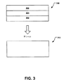
この実現例において、MgOトンネルバリア層214は、互いの上に個々に形成された後、センサ200がポスト熱アニールされてからMgOバリア層214に変換される3つのMgO源層から形成される。図3は、アニールの前のMgOトンネルバリア前層300の拡大図を示す。前層300は、第1の層302、第2または中間層304、および第3の層306を有しており、第2の層304は第1の層302および第3の層306に対して内部である。3つの層302,304,306の各々は約0.1Åから20Åの範囲の厚さを有しており、これらの厚さは、層302,304,306の間で同じまたは異なり得る。
In this implementation, the MgO
第1の層302は、Mg金属層を堆積することにより形成されており、たとえば金属MgターゲットからDCスパッタ堆積プロセスによって形成される。第2の層304は、少量の酸素(O2)によって金属MgターゲットからMg金属を第1の層302上に反応により堆積することによって形成される。R−ox堆積の間の酸素の存在により、Mg金属は少量の酸素でドープされる。R−ox堆積のための堆積パワーは、たとえば約10Wおよび600Wの範囲内である。第3の層306は、たとえばDCスパッタ堆積によって金属MgターゲットからMg金属層を堆積することにより形成される。
The
層302,304,306のうちのいずれかまたはすべてについての堆積温度は約400℃未満である。R−ox堆積またはDC堆積のいずれかについての堆積速度は約0.01〜10Å/sである。
The deposition temperature for any or all of
3つの層302,304,306が形成された後、典型的に読取機積層体全体が形成された後、前層300は熱アニールプロセスに晒され、これにより、3つの層302,304,306がMgOに変換されるとともに層302,304,306をすべてが一緒になるよう融合され、層全体にわたって均質の結晶構造を有するMgOバリア層310が得られる。いくつかの実現例において、アニールの後、層同士の間(たとえば層302と層304との間または層304と層306との間)に界面が発見され得ない。
After the three
さらに、いくつかの実現例において、結果得られたMgO層310の全体にわたって化学構造が均質である。
Furthermore, in some implementations, the chemical structure is homogeneous throughout the resulting
3つのMgO源層を堆積するための例示的なプロセス機器アセンブリは、複数のチャンバおよびターゲットを有しており、TMRセンサのすべての層、いくつかの実現例では磁気読取ヘッドのすべての層を形成するように構成され得る。堆積アセンブリは、複数の高真空物理気相蒸着(PVD:physical vapor deposition)チャンバを有しており、その各々はウェハを内部に受け入れるように構成される。当該チャンバは、DCスパッタリング、RFスパッタリング、または蒸着(evaporation deposition)のために構成され得る。少なくとも1つのターゲットが各チャンバに作用可能に接続されており、材料の源が配置される。スパッタガスから生成されたイオンはターゲットに衝突し、イオン化された材料ビームが作り出され、次いでそれがウェハ面上に堆積される。好適なスパッタガスの例は、アルゴン(Ar)、クリプトン(Kr)、キセノン(Xe)、ヘリウム(He)およびネオン(Ne)を含む。いくつかの実現例では、複数のターゲットが使用される。 An exemplary process equipment assembly for depositing three MgO source layers has multiple chambers and targets, and includes all layers of the TMR sensor, in some implementations all layers of the magnetic read head. Can be configured to form. The deposition assembly has a plurality of high vacuum physical vapor deposition (PVD) chambers, each configured to receive a wafer therein. The chamber can be configured for DC sputtering, RF sputtering, or evaporation deposition. At least one target is operatively connected to each chamber and a source of material is disposed. Ions generated from the sputter gas impinge on the target, creating an ionized material beam that is then deposited on the wafer surface. Examples of suitable sputtering gases include argon (Ar), krypton (Kr), xenon (Xe), helium (He) and neon (Ne). In some implementations, multiple targets are used.
1つの特定の実現例において、第1のMg層はDCスパッタ堆積プロセスを使用して第1のチャンバにおいて形成され、第2のMgO層は酸素源を用いてR−ox堆積を使用して第2のチャンバにおいて形成され、第3のMg層はDCスパッタ堆積を使用して第3のチャンバにおいて形成される。このようなプロセスは、3つのMg層が形成されるので「トリプルMgプロセス」と称される。 In one particular implementation, the first Mg layer is formed in the first chamber using a DC sputter deposition process, and the second MgO layer is formed using R-ox deposition using an oxygen source. Formed in two chambers, and a third Mg layer is formed in the third chamber using DC sputter deposition. Such a process is called a “triple Mg process” because three Mg layers are formed.
Mg/MgO層を形成する前に、AFM層および強磁性ピン層のようなセンサ積層体の他の層が、堆積アセンブリにおいて、上記チャンバのうちのいずれか1つ以上にて基板上に形成され得る。付加的または代替的には、Mg/MgO層を形成した後、強磁性自由層のようなセンサ積層体の他の層がMg/MgO層上にその後で形成され得る。 Prior to forming the Mg / MgO layer, other layers of the sensor stack, such as an AFM layer and a ferromagnetic pinned layer, are formed on the substrate in any one or more of the above chambers in a deposition assembly. obtain. Additionally or alternatively, after forming the Mg / MgO layer, other layers of the sensor stack, such as a ferromagnetic free layer, can subsequently be formed on the Mg / MgO layer.
図4は、本開示に従った、MgOバリア層を形成するための例示的な方法400を提供する。動作402において、Mgターゲットを有する第1のチャンバにおいて、DCスパッタ堆積を介して、強磁性基準層(RL)上に第1の層が堆積される。動作404において、第2のチャンバにおいて反応性酸化(R−ox)堆積を介して第1の層上に第2の層が堆積される。R−ox堆積のためのターゲットはMg金属ターゲットである。R−ox堆積の間に、酸素イオンが第2のチャンバへ提供(たとえば注入)される。酸素は、たとえば圧縮酸素源または圧縮空気源からO2として提供され得るか、または、チャンバにおけるイオン化源に晒される際にO−2を形成するよう解離する源によって提供され得る。酸素イオン源の例は、H2OおよびH2O2を含む。動作406において、第3の層は、Mgターゲットを有する第3のチャンバにおいてDCスパッタ堆積を介して第2の層上に堆積される。動作408において、第1の層、第2の層および第3の層は、たとえば、30分から8時間の間、約150℃から400℃の温度で、アニールプロセスに晒される。
FIG. 4 provides an
図5は、本開示に従った、MgOバリア層を形成するための例示的な方法500を提供する。別の態様で示されなければ、方法500のあるステップおよび/または詳細は方法400と同じまたは同様である。動作502において、Mgターゲットを有する第1のチャンバにおいて、DCスパッタ堆積を介して、強磁性基準層(RL)上に第1の層が堆積される。動作504において、第2のチャンバにおいて反応性酸化(R−ox)堆積を介して第1の層上に第2の層が堆積される。R−ox堆積のためのターゲットはMg金属ターゲットである。O2またはO−2のいずれかとしての酸素がR−ox堆積の間に第2のチャンバへ提供(たとえば注入)される。動作506において、第3の層は、Mgターゲットを有する第2のチャンバにおいてDCスパッタ堆積を介して第2の層上に堆積される。このMgターゲットは、第2の層に使用されたのと同じまたは異なるターゲットであり得る。動作508において、第1の層、第2の層および第3の層はアニールプロセスに晒される。
FIG. 5 provides an
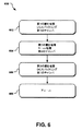
図6は、本開示に従った、MgOバリア層を形成するための例示的な方法600を提供する。別の態様で示されなければ、方法600のあるステップおよび/または詳細は方法400および/または方法500と同じまたは同様である。動作602において、Mgターゲットを有する第1のチャンバにおいて、RFスパッタ堆積を介して、強磁性基準層(RL)上に第1の層が堆積される。動作604において、第2のチャンバにおいて反応性酸化(R−ox)堆積を介して第1の層上に第2の層が堆積される。R−ox堆積のためのターゲットはMg金属ターゲットである。O2またはO−2のいずれかとしての酸素が、R−ox堆積の間に第2のチャンバに提供(たとえば注入)される。動作606において、第3の層は、Mgターゲットを有する第1のチャンバにおいてDCスパッタ堆積を介して第2の層上に堆積される。このMgターゲットは、第1の層に使用されたのと同じまたは異なるターゲットであり得る。動作608において、第1の層、第2の層および第3の層はアニールプロセスに晒される。
FIG. 6 provides an
図7は、本開示に従った、MgOバリア層を形成するための例示的な方法700を提供する。別の態様で示されなければ、方法700のあるステップおよび/または詳細は方法400、方法500および/または方法600と同じまたは同様である。動作702において、Mgターゲットを有する第1のチャンバにおいて、DCスパッタ堆積を介して、強磁性基準層(RL)上に第1の層が堆積される。動作704において、第1のチャンバにおいて反応性酸化(R−ox)堆積を介して第1の層上に第2の層が堆積される。R−ox堆積のためのターゲットはMg金属ターゲットである。このMgターゲットは、第1の層に使用されたのと同じまたは異なるターゲットであり得る。O2またはO−2のいずれかとしての酸素が、R−ox堆積の間にチャンバへ提供(たとえば注入)される。動作706において、第3の層は、Mgターゲットを有する第2のチャンバにおいてDCスパッタ堆積を介して第2の層上に堆積される。このMgターゲットは、第2の層に使用されたのと同じまたは異なるターゲットであり得る。動作708において、第1の層、第2の層および第3の層はアニールプロセスに晒される。
FIG. 7 provides an
方法400、600および700の各々において、第3の層は、酸素が加えられた(すなわち第2の層の堆積のために)チャンバと異なるチャンバにおいて堆積される。第3の層のために第2の層とは異なるチャンバを利用することによって、第3の層の汚染が低減される。
In each of
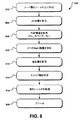
図8は、TMRセンサを形成するための例示的な方法800を提供する。動作802において、シード層は底部シールド上に形成される。動作804において、反強磁性(AFM)層はシード層上に設けられる。動作806において、(ピン層(PL)、スペーサ層(たとえばRu層)および基準層(RL)を含む)SAF構造がAFM層上に設けられる。動作808において、3つのMgO源層がSAF構造の基準層上に設けられ、これらの3つのMgO源層は、たとえば図4の方法400、図5の方法500、図6の方法600または図7の方法700のうちのいずれかによって形成され得る。動作810において、自由層がMgO源層上に形成される。動作812において、キャップ層が自由層上に設けられる。動作814において、頂部シールドがキャップ層上に形成される。動作816において、(MgO源層を含む)全積層体がアニールされて、MgOバリア層を有するTMRセンサが形成される。
FIG. 8 provides an
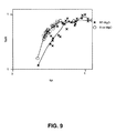
図9は、反応性酸化MgOプロセス(R−ox MgO)によって形成されるMgOバリア層を有するTMRセンサと、従来のRF−MgOプロセスによって形成されるMgOバリアを有するTMRセンサとの両方について、正規化されたRAの関数として正規化されたTMRのグラフを示す。R−ox MgOプロセスはRF−MgOプロセスより高いTMRを示す。 FIG. 9 shows the normality of both a TMR sensor having an MgO barrier layer formed by a reactive oxidized MgO process (R-ox MgO) and a TMR sensor having an MgO barrier formed by a conventional RF-MgO process. Figure 6 shows a graph of normalized TMR as a function of normalized RA. The R-ox MgO process exhibits a higher TMR than the RF-MgO process.
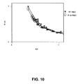
図10は、反応性酸化MgOプロセス(R−ox MgO)によって形成されるMgOバリア層を有するTMRセンサと、従来のRF−MgOプロセスによって形成されるMgOバリア層を有するTMRセンサとの両方について、正規化されたRAの関数として正規化された自由層交換結合(H_ex)のグラフを示す。グラフから、R−ox MgOは自由層交換結合フィールド(H_ex)を低減し得ることが分かる。 FIG. 10 shows both a TMR sensor having a MgO barrier layer formed by a reactive oxidation MgO process (R-ox MgO) and a TMR sensor having a MgO barrier layer formed by a conventional RF-MgO process. FIG. 6 shows a graph of normalized free layer exchange coupling (H_ex) as a function of normalized RA. FIG. From the graph, it can be seen that R-ox MgO can reduce the free layer exchange coupling field (H_ex).
図9および図10の両方は、R−ox MgOプロセスを使用することにより、MgOバリア層の品質が向上することを示す。R−ox MgOプロセスから得られるMgOバリア層は、RF−MgOプロセスによって形成されたMgOバリア層よりも、より均一であり、より平滑であり、より少ないピンホールを有する。さらに、R−ox MgOプロセスによって形成されたMgOバリア層により、得られたTMRセンサは、RF−MgOプロセスによって形成されるMgOバリア層を有するTMRセンサよりも、高いTMRおよび低いH_exを有する。 Both FIG. 9 and FIG. 10 show that the quality of the MgO barrier layer is improved by using the R-ox MgO process. The MgO barrier layer obtained from the R-ox MgO process is more uniform, smoother and has fewer pinholes than the MgO barrier layer formed by the RF-MgO process. Furthermore, due to the MgO barrier layer formed by the R-ox MgO process, the resulting TMR sensor has a higher TMR and lower H_ex than a TMR sensor having an MgO barrier layer formed by the RF-MgO process.
このように、反応性酸化(R−ox)MgO堆積プロセスによって形成されたMgOバリア層のさまざまな特徴を記載した。上記の明細書は、本発明の例示的な実現例の構造および使用の完全な記載を提供する。上記の記載は特定の実現例を提供する。本開示の範囲または精神から逸脱することがなければ、他の実現例が考えられ作製されてもよいということが理解されるべきである。上記の詳細な説明はしたがって、限定的な意味において解釈されるべきではない。本開示はそのようには限定されず、当該開示のさまざまな局面の理解は、提供された例の議論を通じて得られるであろう。 Thus, various features of the MgO barrier layer formed by the reactive oxidation (R-ox) MgO deposition process have been described. The above specification provides a complete description of the structure and use of exemplary implementations of the invention. The above description provides a specific implementation. It should be understood that other implementations may be envisioned and made without departing from the scope or spirit of the present disclosure. The above detailed description is, therefore, not to be construed in a limiting sense. The present disclosure is not so limited, and an understanding of various aspects of the disclosure will be gained through a discussion of the examples provided.
別の態様で示されなければ、機構のサイズ、量および物理的性質を示すすべての数字は、「約」という用語によって修飾されると理解されるべきである。したがって、それと反対に示されなければ、記載される任意の数値パラメータは、本願明細書において開示された教示を利用する当業者によって得るよう求められる所望の特性に依存して変化し得る近似である。 Unless otherwise indicated, it should be understood that all numbers indicating the size, amount and physical properties of features are modified by the term “about”. Thus, unless indicated to the contrary, any numerical parameter described is an approximation that may vary depending on the desired properties sought to be obtained by one of ordinary skill in the art using the teachings disclosed herein. .
本願明細書において使用されるように、「1つの(a;an)」および「その(the)」という単数形は、内容が明白に別の態様を示さなければ、複数の指示物を有する実現例を包含する。この明細書および添付の特許請求の範囲において使用されるように、「または」という用語は一般に、内容が明白に別の態様を示さなければ、「および/または」を含む意味で使用される。 As used herein, the singular forms “a (an)” and “the” have multiple indications unless the content clearly indicates otherwise. Examples are included. As used in this specification and the appended claims, the term “or” is generally employed in its sense including “and / or” unless the content clearly dictates otherwise.
「底部」、「下部」、「頂部」、「上部」、「下」、「下方」、「上方」、「の上」、「上」などを含むがこれらに限定されない空間に関連する用語は、本願明細書において使用される場合、ある要素の別の要素に対する空間的関係を説明するために、記載の容易さのために利用される。そのような空間に関連する用語は、図において示されるとともに本願明細書において記載された特定の方位に加えて、デバイスの異なる方位を包含する。たとえば、図において示される構造が回転またはひっくり返される場合、他の要素の下または下側として以前に記載された部分は、当該他の要素の上または上側に存在することになる。 Terms related to space including but not limited to "bottom", "bottom", "top", "top", "bottom", "downward", "upper", "top", "top", etc. As used herein, it is used for ease of description to describe the spatial relationship of one element to another. Terminology related to such space encompasses different orientations of the device in addition to the particular orientation shown in the figures and described herein. For example, if the structure shown in the figure is rotated or flipped, the portion previously described as below or below another element will be above or above that other element.
本発明の精神および範囲から逸脱することがなければ本発明の多くの実現例が作製され得るので、本発明は添付の特許請求の範囲内に存在する。更に、記載される特許請求の範囲から逸脱することがなければ、異なる実現例の構造的特徴は、さらに別の実現例において組み合わせられてもよい。 Since many implementations of the invention can be made without departing from the spirit and scope of the invention, the invention resides in the claims hereinafter appended. Moreover, structural features of different implementations may be combined in yet other implementations without departing from the scope of the claims as described.
Claims (16)
Mgターゲットから第1のMgO源層を堆積するステップと、
酸素の存在下において反応性酸化物堆積プロセスを使用して、Mgターゲットから前記第1のMgO源層上に第2のMgO源層を堆積するステップと、
Mgターゲットから前記第2のMgO源層上に第3のMgO源層を堆積するステップと、
MgOバリア層を形成するよう、前記第1のMgO源層、前記第2のMgO源層および前記第3のMgO源層をアニールするステップとを含む、方法。 A method for producing a MgO barrier layer for a TMR sensor, comprising:
Depositing a first MgO source layer from a Mg target;
Depositing a second MgO source layer on the first MgO source layer from an Mg target using a reactive oxide deposition process in the presence of oxygen;
Depositing a third MgO source layer on the second MgO source layer from a Mg target;
Annealing the first MgO source layer, the second MgO source layer, and the third MgO source layer to form an MgO barrier layer.
第1のチャンバにおいて第1のMg層を堆積するステップと、
前記第1のチャンバまたは前記第1のチャンバとは異なる第2のチャンバにおいて、酸素の存在下で、反応性酸化物堆積プロセスを使用して前記第1のMg層上に第2のMg層を堆積するステップと、
前記第1のチャンバ、前記第2のチャンバまたは第3のチャンバのいずれかにおいて前記第2のMgO層上に第3のMg層を堆積するステップと、
MgOバリア層を形成するよう前記第1の層、前記第2の層および前記第3の層をアニールするステップとを含む、方法。 A method for producing a MgO barrier layer for a TMR sensor, comprising:
Depositing a first Mg layer in a first chamber;
A second Mg layer is formed on the first Mg layer using a reactive oxide deposition process in the presence of oxygen in the first chamber or a second chamber different from the first chamber. Depositing steps;
Depositing a third Mg layer on the second MgO layer in either the first chamber, the second chamber or a third chamber;
Annealing the first layer, the second layer, and the third layer to form an MgO barrier layer.
Applications Claiming Priority (2)
| Application Number | Priority Date | Filing Date | Title |
|---|---|---|---|
| US14/699,190 | 2015-04-29 | ||
| US14/699,190 US9890449B2 (en) | 2015-04-29 | 2015-04-29 | Methods of forming MgO barrier layer |
Publications (2)
| Publication Number | Publication Date |
|---|---|
| JP2016212941A true JP2016212941A (en) | 2016-12-15 |
| JP2016212941A5 JP2016212941A5 (en) | 2019-01-24 |
Family
ID=57205539
Family Applications (1)
| Application Number | Title | Priority Date | Filing Date |
|---|---|---|---|
| JP2015242007A Pending JP2016212941A (en) | 2015-04-29 | 2015-12-11 | METHODS OF MAKING MgO BARRIER LAYER FOR TMR SENSOR |
Country Status (4)
| Country | Link |
|---|---|
| US (2) | US9890449B2 (en) |
| JP (1) | JP2016212941A (en) |
| KR (2) | KR20160128895A (en) |
| CN (1) | CN106098082A (en) |
Families Citing this family (3)
| Publication number | Priority date | Publication date | Assignee | Title |
|---|---|---|---|---|
| US10229705B2 (en) * | 2017-01-24 | 2019-03-12 | International Business Machines Corporation | Shorting tolerant tunnel valve head and circuit |
| KR102470367B1 (en) * | 2017-11-24 | 2022-11-24 | 삼성전자주식회사 | Method of manufacturing a magnetoresistive random access device |
| US10837105B1 (en) | 2019-01-03 | 2020-11-17 | Seagate Technology Llc | Multilayer barrier and method of formation |
Citations (4)
| Publication number | Priority date | Publication date | Assignee | Title |
|---|---|---|---|---|
| JP2007173843A (en) * | 2005-12-22 | 2007-07-05 | Magic Technologies Inc | Tunnel barrier layer, its forming method, mtj element, and its manufacturing method |
| JP2008091484A (en) * | 2006-09-29 | 2008-04-17 | Toshiba Corp | Method and device for manufacturing magnetoresistive effect element |
| JP2008263031A (en) * | 2007-04-11 | 2008-10-30 | Toshiba Corp | Magnetoresistance effect element, its manufacturing method, magnetic memory device provided with magnetoresistance effect element and its manufacturing method |
| JP2008300840A (en) * | 2007-05-29 | 2008-12-11 | Headway Technologies Inc | Pined layer and tmr sensor using the same, and method of manufacturing tmr sensor |
Family Cites Families (14)
| Publication number | Priority date | Publication date | Assignee | Title |
|---|---|---|---|---|
| JPH07326783A (en) * | 1994-05-30 | 1995-12-12 | Canon Inc | Formation of photovoltatic element and thin film manufacturing device used therefor |
| US5460704A (en) * | 1994-09-28 | 1995-10-24 | Motorola, Inc. | Method of depositing ferrite film |
| JP2002314166A (en) | 2001-04-16 | 2002-10-25 | Nec Corp | Magnetoresistance effect element and its manufacturing method |
| US6841395B2 (en) | 2002-11-25 | 2005-01-11 | International Business Machines Corporation | Method of forming a barrier layer of a tunneling magnetoresistive sensor |
| JP2005042200A (en) * | 2003-07-21 | 2005-02-17 | Korea Electrotechnology Research Inst | Reactive sputtering deposition device and method |
| KR100628928B1 (en) | 2003-07-21 | 2006-09-27 | 한국전기연구원 | Apparatus for reactive sputtering deposition |
| US7820020B2 (en) * | 2005-02-03 | 2010-10-26 | Applied Materials, Inc. | Apparatus for plasma-enhanced physical vapor deposition of copper with RF source power applied through the workpiece with a lighter-than-copper carrier gas |
| CN100346524C (en) * | 2005-07-28 | 2007-10-31 | 复旦大学 | Device and method for preparing solid thin-membrane lithium battery by in-situ deposition |
| US7780820B2 (en) | 2005-11-16 | 2010-08-24 | Headway Technologies, Inc. | Low resistance tunneling magnetoresistive sensor with natural oxidized double MgO barrier |
| US7535069B2 (en) * | 2006-06-14 | 2009-05-19 | International Business Machines Corporation | Magnetic tunnel junction with enhanced magnetic switching characteristics |
| FR2910716B1 (en) * | 2006-12-26 | 2010-03-26 | Commissariat Energie Atomique | MULTILAYER MAGNETIC DEVICE, METHOD FOR PRODUCING THE SAME, MAGNETIC FIELD SENSOR, MAGNETIC MEMORY AND LOGIC HOLDER USING SUCH A DEVICE |
| US7488609B1 (en) | 2007-11-16 | 2009-02-10 | Hitachi Global Storage Technologies Netherlands B.V. | Method for forming an MgO barrier layer in a tunneling magnetoresistive (TMR) device |
| US20130134032A1 (en) | 2008-06-25 | 2013-05-30 | Canon Anelva Corporation | Method of fabricating and apparatus of fabricating tunnel magnetic resistive element |
| EP2568305B1 (en) * | 2011-09-09 | 2016-03-02 | Crocus Technology S.A. | Magnetic tunnel junction with an improved tunnel barrier |
-
2015
- 2015-04-29 US US14/699,190 patent/US9890449B2/en active Active
- 2015-10-30 CN CN201510729444.3A patent/CN106098082A/en active Pending
- 2015-12-07 KR KR1020150173080A patent/KR20160128895A/en active Application Filing
- 2015-12-11 JP JP2015242007A patent/JP2016212941A/en active Pending
-
2017
- 2017-11-30 US US15/827,755 patent/US20180094346A1/en not_active Abandoned
-
2018
- 2018-04-03 KR KR1020180038680A patent/KR101977795B1/en active IP Right Grant
Patent Citations (4)
| Publication number | Priority date | Publication date | Assignee | Title |
|---|---|---|---|---|
| JP2007173843A (en) * | 2005-12-22 | 2007-07-05 | Magic Technologies Inc | Tunnel barrier layer, its forming method, mtj element, and its manufacturing method |
| JP2008091484A (en) * | 2006-09-29 | 2008-04-17 | Toshiba Corp | Method and device for manufacturing magnetoresistive effect element |
| JP2008263031A (en) * | 2007-04-11 | 2008-10-30 | Toshiba Corp | Magnetoresistance effect element, its manufacturing method, magnetic memory device provided with magnetoresistance effect element and its manufacturing method |
| JP2008300840A (en) * | 2007-05-29 | 2008-12-11 | Headway Technologies Inc | Pined layer and tmr sensor using the same, and method of manufacturing tmr sensor |
Also Published As
| Publication number | Publication date |
|---|---|
| KR101977795B1 (en) | 2019-05-13 |
| KR20160128895A (en) | 2016-11-08 |
| US9890449B2 (en) | 2018-02-13 |
| CN106098082A (en) | 2016-11-09 |
| KR20180037613A (en) | 2018-04-12 |
| US20180094346A1 (en) | 2018-04-05 |
| US20160319419A1 (en) | 2016-11-03 |
Similar Documents
| Publication | Publication Date | Title |
|---|---|---|
| JP5739833B2 (en) | Data sensing element, magnetic element and method | |
| JP6100990B2 (en) | Magnetoresistive sensor and manufacturing method thereof | |
| JP5529648B2 (en) | Magnetic sensor laminate, film formation method thereof, film formation control program, and recording medium | |
| US6631055B2 (en) | Tunnel valve flux guide structure formed by oxidation of pinned layer | |
| JP5897448B2 (en) | Magnetic sensor having CoFeBTa in fixed layer structure and free layer structure | |
| JP3601690B2 (en) | Magnetoresistive element and manufacturing method thereof, magnetoresistive head, magnetic recording device, magnetoresistive memory element | |
| JP5599738B2 (en) | Magnetoresistive element and method for forming the same | |
| US8373948B2 (en) | Tunnel magnetoresistance (TMR) structures with MGO barrier and methods of making same | |
| US8077435B1 (en) | Current perpendicular-to-plane read sensor with back shield | |
| CN100369116C (en) | Magnetic head and magnetic recording/reproducing device | |
| US10354707B2 (en) | Composite seed layer | |
| CN101499514A (en) | Magnetoresistive element and method of manufacturing the same | |
| US10354681B1 (en) | Tunnel magnetoresistance read head including side shields containing nanocrystalline ferromagnetic particles | |
| US9679589B2 (en) | Magnetoresistive sensor with enhanced uniaxial anisotropy | |
| CN101499515A (en) | Magnetoresistive element and method of manufacturing the same | |
| GB2525740A (en) | TMR/CPP reader for narrow reader gap application | |
| US20080151439A1 (en) | Tmr sensor having magnesium/magnesium oxide tunnel barrier | |
| JP2015015068A (en) | CURRENT-PERPENDICULAR-TO-THE PLANE (CPP) MAGNETORESISTIVE SENSORS WITH REFERENCE LAYER CONSISTING OF MULTI LAYER, INCLUDING CRYSTALLINE CoFeX LAYER AND HEUSLER TYPE ALLOY LAYER | |
| JP2013004166A (en) | Magnetic sensor having hard bias seed structure | |
| KR101977795B1 (en) | Methods of forming mgo barrier layer | |
| WO2001093286A1 (en) | Magnetic thin film, production method therefor, evaluation method therefor and magnetic head using it, magnetic refcording device and magnetic device | |
| JP2014107006A (en) | CURRENT-PERPENDICULAR-TO-THE-PLANE (CPP) MAGNETORESISTIVE (MR) SENSOR WITH HARD MAGNET BIASING STRUCTURE HAVING MgO INSULATING LAYER | |
| JP2000500292A (en) | Magnetic field sensor and method of manufacturing magnetic field sensor | |
| US6398924B1 (en) | Spin valve sensor with improved pinning field between nickel oxide (NiO) pinning layer and pinned layer | |
| JP2006186345A (en) | Film and method for producing nano-particles for magnetoresistive device |
Legal Events
| Date | Code | Title | Description |
|---|---|---|---|
| A521 | Request for written amendment filed |
Free format text: JAPANESE INTERMEDIATE CODE: A523 Effective date: 20181207 |
|
| A621 | Written request for application examination |
Free format text: JAPANESE INTERMEDIATE CODE: A621 Effective date: 20181207 |
|
| A977 | Report on retrieval |
Free format text: JAPANESE INTERMEDIATE CODE: A971007 Effective date: 20190711 |
|
| A131 | Notification of reasons for refusal |
Free format text: JAPANESE INTERMEDIATE CODE: A131 Effective date: 20190723 |
|
| A601 | Written request for extension of time |
Free format text: JAPANESE INTERMEDIATE CODE: A601 Effective date: 20191021 |
|
| A601 | Written request for extension of time |
Free format text: JAPANESE INTERMEDIATE CODE: A601 Effective date: 20191223 |
|
| A521 | Request for written amendment filed |
Free format text: JAPANESE INTERMEDIATE CODE: A523 Effective date: 20200121 |
|
| A02 | Decision of refusal |
Free format text: JAPANESE INTERMEDIATE CODE: A02 Effective date: 20200218 |