JP5529648B2 - Magnetic sensor laminate, film formation method thereof, film formation control program, and recording medium - Google Patents
Magnetic sensor laminate, film formation method thereof, film formation control program, and recording medium Download PDFInfo
- Publication number
- JP5529648B2 JP5529648B2 JP2010149407A JP2010149407A JP5529648B2 JP 5529648 B2 JP5529648 B2 JP 5529648B2 JP 2010149407 A JP2010149407 A JP 2010149407A JP 2010149407 A JP2010149407 A JP 2010149407A JP 5529648 B2 JP5529648 B2 JP 5529648B2
- Authority
- JP
- Japan
- Prior art keywords
- layer
- substrate
- forming
- magnetic
- stack
- Prior art date
- Legal status (The legal status is an assumption and is not a legal conclusion. Google has not performed a legal analysis and makes no representation as to the accuracy of the status listed.)
- Active
Links
Images


Classifications
-
- G—PHYSICS
- G11—INFORMATION STORAGE
- G11B—INFORMATION STORAGE BASED ON RELATIVE MOVEMENT BETWEEN RECORD CARRIER AND TRANSDUCER
- G11B5/00—Recording by magnetisation or demagnetisation of a record carrier; Reproducing by magnetic means; Record carriers therefor
- G11B5/127—Structure or manufacture of heads, e.g. inductive
- G11B5/33—Structure or manufacture of flux-sensitive heads, i.e. for reproduction only; Combination of such heads with means for recording or erasing only
- G11B5/39—Structure or manufacture of flux-sensitive heads, i.e. for reproduction only; Combination of such heads with means for recording or erasing only using magneto-resistive devices or effects
- G11B5/3903—Structure or manufacture of flux-sensitive heads, i.e. for reproduction only; Combination of such heads with means for recording or erasing only using magneto-resistive devices or effects using magnetic thin film layers or their effects, the films being part of integrated structures
- G11B5/3906—Details related to the use of magnetic thin film layers or to their effects
- G11B5/3929—Disposition of magnetic thin films not used for directly coupling magnetic flux from the track to the MR film or for shielding
- G11B5/3932—Magnetic biasing films
-
- G—PHYSICS
- G01—MEASURING; TESTING
- G01R—MEASURING ELECTRIC VARIABLES; MEASURING MAGNETIC VARIABLES
- G01R33/00—Arrangements or instruments for measuring magnetic variables
- G01R33/02—Measuring direction or magnitude of magnetic fields or magnetic flux
- G01R33/06—Measuring direction or magnitude of magnetic fields or magnetic flux using galvano-magnetic devices
- G01R33/09—Magnetoresistive devices
- G01R33/098—Magnetoresistive devices comprising tunnel junctions, e.g. tunnel magnetoresistance sensors
-
- G—PHYSICS
- G11—INFORMATION STORAGE
- G11B—INFORMATION STORAGE BASED ON RELATIVE MOVEMENT BETWEEN RECORD CARRIER AND TRANSDUCER
- G11B5/00—Recording by magnetisation or demagnetisation of a record carrier; Reproducing by magnetic means; Record carriers therefor
- G11B5/127—Structure or manufacture of heads, e.g. inductive
- G11B5/31—Structure or manufacture of heads, e.g. inductive using thin films
- G11B5/3163—Fabrication methods or processes specially adapted for a particular head structure, e.g. using base layers for electroplating, using functional layers for masking, using energy or particle beams for shaping the structure or modifying the properties of the basic layers
-
- G—PHYSICS
- G11—INFORMATION STORAGE
- G11B—INFORMATION STORAGE BASED ON RELATIVE MOVEMENT BETWEEN RECORD CARRIER AND TRANSDUCER
- G11B5/00—Recording by magnetisation or demagnetisation of a record carrier; Reproducing by magnetic means; Record carriers therefor
- G11B5/127—Structure or manufacture of heads, e.g. inductive
- G11B5/33—Structure or manufacture of flux-sensitive heads, i.e. for reproduction only; Combination of such heads with means for recording or erasing only
- G11B5/39—Structure or manufacture of flux-sensitive heads, i.e. for reproduction only; Combination of such heads with means for recording or erasing only using magneto-resistive devices or effects
- G11B5/3903—Structure or manufacture of flux-sensitive heads, i.e. for reproduction only; Combination of such heads with means for recording or erasing only using magneto-resistive devices or effects using magnetic thin film layers or their effects, the films being part of integrated structures
- G11B5/398—Specially shaped layers
-
- H—ELECTRICITY
- H10—SEMICONDUCTOR DEVICES; ELECTRIC SOLID-STATE DEVICES NOT OTHERWISE PROVIDED FOR
- H10N—ELECTRIC SOLID-STATE DEVICES NOT OTHERWISE PROVIDED FOR
- H10N50/00—Galvanomagnetic devices
- H10N50/01—Manufacture or treatment
-
- H—ELECTRICITY
- H10—SEMICONDUCTOR DEVICES; ELECTRIC SOLID-STATE DEVICES NOT OTHERWISE PROVIDED FOR
- H10N—ELECTRIC SOLID-STATE DEVICES NOT OTHERWISE PROVIDED FOR
- H10N50/00—Galvanomagnetic devices
- H10N50/10—Magnetoresistive devices
Description
本発明は、磁気抵抗素子(リーダースタック)の両側に、バイアス磁界を与える磁性層を備えた磁気センサ積層体、成膜方法、成膜制御プログラムおよび記録媒体に関する。 The present invention relates to a magnetic sensor stack, a film forming method, a film forming control program, and a recording medium, each having a magnetic layer for applying a bias magnetic field on both sides of a magnetoresistive element (reader stack).
近年のハードディスク駆動装置(HDD)の大容量化に伴い、外部磁界の変動に応じて電気抵抗が変化する素子を用いた磁気抵抗(MR)ヘッドが注目されている。特に巨大磁気抵抗(GMR)ヘッドやトンネル磁気抵抗(TMR)ヘッドは感度が非常に高く、磁気ディスクの記録密度を高めることができる。さらに高密度記録化に伴って、MRヘッドの縮小化が進められている。 2. Description of the Related Art With the recent increase in capacity of hard disk drive devices (HDD), a magnetoresistive (MR) head using an element whose electric resistance changes in accordance with fluctuations in an external magnetic field has attracted attention. In particular, giant magnetoresistive (GMR) heads and tunneling magnetoresistive (TMR) heads have very high sensitivity and can increase the recording density of the magnetic disk. As the recording density becomes higher, the MR head is being reduced.
MRヘッドは、バイアス磁界を与える磁性層によって二側面が囲まれたMR素子(リーダースタック)を備えている。リーダースタックを縮小すると、当然にバイアス磁界を与える磁性層が利用できる空間も規制される。磁性層の体積、およびリーダースタックの端部と対向する面の面積を縮小すると、バイアス磁界が減少する。 The MR head includes an MR element (reader stack) surrounded on two sides by a magnetic layer that applies a bias magnetic field. When the leader stack is reduced, the space in which the magnetic layer that provides the bias magnetic field can be used is also restricted. When the volume of the magnetic layer and the area of the surface facing the edge of the reader stack are reduced, the bias magnetic field is reduced.
リーダースタックに対向する面はリードギャップ〔磁気トンネル接合(MTJ)または巨大磁気抵抗(GMR)積層を囲む2個のシールドの間の距離〕およびストライプ高さ〔記録媒体表面に垂直なリーダースタックの横寸法〕によって決定される。リードギャップの減少はリニア(トラック上の)分解能の増大のために必要であり、ストライプ高さの減少はトラックエッジへの感度を低下させるために必要なリーダ幅の減少に付随する。 The face opposite the leader stack is the lead gap [distance between the two shields surrounding the magnetic tunnel junction (MTJ) or giant magnetoresistive (GMR) stack) and the stripe height [the side of the leader stack perpendicular to the recording medium surface]. Dimension]. A reduction in the read gap is necessary for increased linear (on track) resolution, and a reduction in stripe height is accompanied by a reduction in the leader width required to reduce sensitivity to track edges.
ハードディスクドライブ(HDD)の面密度の増大は、構成部品の大きさを調整すること、および信号処理を改良することによりなされる。記録媒体のビットをより小さくするため、すなわち、トラック/インチ(TPI)およびビット/インチ(BPI)を単位とする密度を増大させるために、結晶粒をより小さくし、直径分布をより密にする技術開発が進められている。より小さい磁気領域に記録し、かつより小さい磁気領域から読み取るために、書込装置および読取装置の両方が縮小される。特に、解像度を増大し、より高いBPIの記録を達成すべく、TPIを増大し、シールド間距離を減少させると同時に、読取装置の幅が狭く設定される。 Increasing the surface density of hard disk drives (HDDs) is done by adjusting the size of components and improving signal processing. In order to make the bits of the recording medium smaller, ie to increase the density in units of tracks / inch (TPI) and bits / inch (BPI), the grains are made smaller and the diameter distribution is made denser. Technology development is underway. Both the writer and the reader are scaled down to record in and read from the smaller magnetic area. In particular, in order to increase resolution and achieve higher BPI recording, the TPI is increased and the distance between shields is reduced, while the width of the reader is set narrower.
典型的なセンサ構造は、反強磁性(AFM)ピニング層、シンセティックアンチフェロ層(SAF)、非磁性スペーサまたはトンネル絶縁体、および強磁性フリー層からなる。また、シード層およびキャッピング層も種々の目的で使用される。SAFは、薄いスペーサ層を介して反方向に結合した2つの強磁性体からなる。SAFの強磁性体は、AFMと接触しているピンド層と、非磁性スペーサまたはトンネル絶縁体と接触しているリファレンス層とを含む。リーダースタックを通じた抵抗変化は、リファレンス層とフリー層との間の磁化の相対的方向によって決定される。フリー層は、磁界にバイアスがかけられ、リファレンス層と直角を成すように配向されている。この構成により読み込み感度は非常に高くなり、記憶媒体からの外部磁場に対して線形応答を得ることができる。バイアス磁界は、「ハードバイアス」とも称され、ディスクドライブの寿命を通して一定に維持されることが期待される。またハードバイアスは、フリー層に磁区が発生することを防ぐ役割を持つ。磁気抵抗素子およびハードバイアス積層体は共に、2つの厚い軟磁性シールド間に挟まれている。 A typical sensor structure consists of an antiferromagnetic (AFM) pinning layer, a synthetic antiferro layer (SAF), a nonmagnetic spacer or tunnel insulator, and a ferromagnetic free layer. A seed layer and a capping layer are also used for various purposes. SAF consists of two ferromagnets coupled in opposite directions via a thin spacer layer. The SAF ferromagnet includes a pinned layer in contact with the AFM and a reference layer in contact with a non-magnetic spacer or tunnel insulator. The resistance change through the leader stack is determined by the relative direction of magnetization between the reference layer and the free layer. The free layer is biased with a magnetic field and is oriented perpendicular to the reference layer. With this configuration, the reading sensitivity becomes very high, and a linear response can be obtained with respect to the external magnetic field from the storage medium. The bias magnetic field, also referred to as “hard bias”, is expected to remain constant throughout the life of the disk drive. Further, the hard bias has a role of preventing the occurrence of magnetic domains in the free layer. Both the magnetoresistive element and the hard bias stack are sandwiched between two thick soft magnetic shields.
単純なハードバイアス積層体は、CrまたはWなどの下地層と、CoPtまたはCoCrPtなどから構成される磁性層と、Cr、RuもしくはTaなどから作成されるキャッピング層とからなる。磁性層の保磁力(Hc)は、特に高い動作温度での外部磁場によるスイッチングを防止するために、159.5kA/m(2000エルステッド(Oe))以上の値が望ましい。 A simple hard bias laminate includes an underlayer such as Cr or W, a magnetic layer made of CoPt or CoCrPt, and a capping layer made of Cr, Ru, Ta, or the like. The coercive force (Hc) of the magnetic layer is preferably 159.5 kA / m (2000 Oersted (Oe)) or more in order to prevent switching by an external magnetic field at a particularly high operating temperature.
磁性層結晶粒の一部に磁化反転が生じると、バイアス磁界の著しい減少を招く可能性があり、またセンサにおけるノイズを誘発する。リードギャップサイズの縮小は、シールド間に適用できるハードバイアス積層体の厚さの減少につながる。バイアス磁界は、磁性層の残留磁化と厚さとの積(Mrt)に比例するため、厚さtが減少すると、フリー層のバイアス印加が不十分となりうる。さらに、磁性層とシールド層とが近接することにより、シールド層への漏れ磁束が増加し、接合壁面(リーダースタックとハードバイアス積層体の境目)におけるバイアス磁界がさらに減少することになる。 When magnetization reversal occurs in a part of the crystal grains of the magnetic layer, the bias magnetic field may be significantly reduced, and noise in the sensor is induced. The reduction in the lead gap size leads to a reduction in the thickness of the hard bias stack that can be applied between the shields. Since the bias magnetic field is proportional to the product (Mrt) of the remanent magnetization and the thickness of the magnetic layer, if the thickness t decreases, the bias application to the free layer may be insufficient. Furthermore, when the magnetic layer and the shield layer are close to each other, the leakage magnetic flux to the shield layer is increased, and the bias magnetic field on the bonding wall surface (the boundary between the leader stack and the hard bias laminate) is further reduced.
磁界を増加させる方法の一つは、接合壁面において磁性層をフリー層から隔てている絶縁層の厚さを減少させることである。しかしながら、低リーク電流および高降伏電圧が要求されることから、絶縁体の厚みを薄くするには制限がある。磁性層をフェライトなどの絶縁材料で作成することが可能であり、それにより絶縁層を省略したり、あるいはその厚さを3nm以下まで減少させることができる。しかしながら、ほとんどの絶縁性磁性フェライトの飽和磁化および保磁力は、Co−Pt合金のものに劣る傾向がある。組成および結晶成長も制御がはるかに困難である。 One way to increase the magnetic field is to reduce the thickness of the insulating layer separating the magnetic layer from the free layer at the junction wall. However, since a low leakage current and a high breakdown voltage are required, there is a limit to reducing the thickness of the insulator. The magnetic layer can be made of an insulating material such as ferrite, thereby eliminating the insulating layer or reducing its thickness to 3 nm or less. However, the saturation magnetization and coercivity of most insulating magnetic ferrites tend to be inferior to those of Co—Pt alloys. Composition and crystal growth are also much more difficult to control.
現在のCoPtベースのハードバイアス積層体は、2次元等方性である。面内において、いかなる方向に沿った保磁力Hcも等しく、すなわち磁気異方性の大きさを表すOR(オリエンテーションレシオ;ストライプ高さ方向に対して面内垂直方向の保磁力/ストライプ高さ方向の保磁力の比)で表すとOR=1である。CoPtの六方晶c軸は、面内でランダムである。しかしながら、多数の結晶粒間の交換結合により、比較的高い角形比(0.85以上)が実現できる。接合壁面では、平均磁界がフリー層に向けられる。ストライプ高さが減少すると、接合壁面にある結晶粒は減少し、それにより磁束をフリー層に向けるのがより難しくなる。これは、前述の結晶粒のc軸がフリー層に向けられていないときに顕著である。もしもc軸を接合壁面に向けて配向できれば、ストライプ高さ(奥行き)の結晶粒径に対する比率はもはや問題ではなくなる。さらに、同じ厚みtに対するMrが増加し、より高いバイアス磁界を得ることができる。より多くの磁束が接合壁面上に集束され、ハードバイアス積層体の側端部で損失する磁束はより少なくなる。 Current CoPt-based hard bias stacks are two-dimensional isotropic. In the plane, the coercive force Hc along any direction is equal, that is, the OR (orientation ratio) indicating the magnitude of magnetic anisotropy; the coercive force in the direction perpendicular to the stripe height direction / the direction of the stripe height When expressed in terms of the coercive force ratio, OR = 1. The hexagonal c-axis of CoPt is random in the plane. However, a relatively high squareness ratio (0.85 or more) can be realized by exchange coupling between a large number of crystal grains. At the joining wall, an average magnetic field is directed to the free layer. As the stripe height decreases, the crystal grains on the bonding walls decrease, thereby making it more difficult to direct the magnetic flux to the free layer. This is remarkable when the c-axis of the crystal grain is not directed to the free layer. If the c-axis can be oriented toward the bonding wall, the ratio of stripe height (depth) to crystal grain size is no longer a problem. Furthermore, Mr increases for the same thickness t, and a higher bias magnetic field can be obtained. More magnetic flux is focused on the junction walls and less magnetic flux is lost at the side edges of the hard bias stack.
浮上面(Air Bearing Surface;以下、「ABS面」という。)から見ると、読取装置全体の幅は、記録されたトラックに対して垂直であり、厚さはトラックに対して平行である。読取装置は、ABS面に対して垂直に、ABS面から離れてストライプ高さ(奥行き)と称される高さまで延びる。読取装置の幅、積層体の厚さ、およびストライプ高さによって、読取装置の三次元寸法が定まる。所与の幅に対する最適なストライプ高さは、通常その幅の1.5倍よりも低い。これまでに列挙されたように読取装置を構成する多くの層が存在し、これにより、得ることのできる厚さの最小値が制限される。 When viewed from the air bearing surface (hereinafter referred to as “ABS surface”), the width of the entire reading device is perpendicular to the recorded track, and the thickness is parallel to the track. The reader extends perpendicular to the ABS surface and away from the ABS surface to a height called the stripe height (depth). The three-dimensional dimensions of the reader are determined by the width of the reader, the thickness of the stack, and the stripe height. The optimum stripe height for a given width is usually less than 1.5 times that width. There are many layers that make up the reader as listed so far, which limits the minimum thickness that can be obtained.
例えば、上記AFM層があまりにも薄く成膜されると、その層は熱的に不安定になり、SAFのピンド層の磁化方向を十分に固定することができない。すなわち、交換バイアスは減少する。さらに、横方向寸法が減少すると、寸法効果が熱的に有限なものとなり、また読取装置の安定性に悪影響を及ぼす。一般に使用されるIr−Mn合金に関しては、大部分の結晶粒が適切な寸法(30nm以上)であると考えられ、厚さが適切であれば(5nm以上)、50nmより大きい横方向寸法は問題にならない。したがって、AFM層が単結晶でなければ、装置の中に不安定な結晶粒が形成されやすい。 For example, if the AFM layer is formed too thin, the layer becomes thermally unstable, and the magnetization direction of the pinned layer of the SAF cannot be sufficiently fixed. That is, the exchange bias decreases. Furthermore, as the lateral dimension decreases, the dimensional effect becomes thermally finite and adversely affects the stability of the reader. For commonly used Ir-Mn alloys, the majority of grains are considered to be of appropriate dimensions (30 nm or more), and if the thickness is appropriate (5 nm or more), lateral dimensions greater than 50 nm are problematic. do not become. Therefore, if the AFM layer is not a single crystal, unstable crystal grains are likely to be formed in the device.
Crシード層は、(110)格子面で成長し、また長手媒体におけるORの研究から、OR>1が達成されるのはCr(002)格子面の場合のみであり、その上にCoPt(1120)が形成される。〔110〕方向と〔1−10〕方向のエピタキシャル関係は、CoPt((1120)格子面のうち、c軸方向の格子定数が0.41nmで、c軸に垂直な格子軸の格子定数が0.43nmである)に対して、エネルギー的に等価となる。異方性応力によりCr格子が面内で変形する場合のみ、特定の方向が好ましい。Simionら(特許文献1参照)は、MgOおよびNiAlなどの異なるシード層を提案している。記録媒体の研究において、双方の下地層は2次元c軸配列を提供することが実証されている。 The Cr seed layer is grown on the (110) lattice plane, and from the study of OR in the longitudinal media, OR> 1 is achieved only for the Cr (002) lattice plane on which CoPt (1120 ) Is formed. The epitaxial relationship between the [110] direction and the [1-10] direction is such that, among the CoPt ((1120) lattice planes, the lattice constant in the c-axis direction is 0.41 nm and the lattice constant perpendicular to the c-axis is 0. .43 nm) in terms of energy. A specific direction is preferred only when the Cr lattice is deformed in-plane by anisotropic stress. Simion et al. (See Patent Document 1) propose different seed layers such as MgO and NiAl. In the study of recording media, it has been demonstrated that both underlayers provide a two-dimensional c-axis array.
Larsonら(特許文献2参照)は、素子接合壁へ向いた優位な磁気異方性を有する磁気抵抗素子を備えた読み取りセンサを開示している。また、San Hoら(特許文献3参照)は、c軸方向がHCP磁気バイアス積層体の角度によって制限される可能を明らかにしている。すなわち、双方の明細書では、斜めスパッタを利用したCoPt合金の成膜によって、磁気異方性を実現できることが開示されている。傾めスパッタは、最も適度なHc ORが1.2未満であるにもかかわらず、Shibamotoら(特許文献6参照)は、長手媒体に配向を与える際にも利用している。初期の窒化Nbまたは窒化Taシード層(異方性許容層)では、剛性円形ディスク内の円周方向に沿って媒体の磁気異方性をもたせるために斜め成膜している。 Larson et al. (See Patent Document 2) discloses a read sensor including a magnetoresistive element having a superior magnetic anisotropy toward the element bonding wall. San Ho et al. (See Patent Document 3) clarifies that the c-axis direction may be limited by the angle of the HCP magnetic bias stack. That is, both specifications disclose that magnetic anisotropy can be realized by forming a CoPt alloy using oblique sputtering. Although tilted sputtering has the most appropriate Hc OR of less than 1.2, Shibamoto et al. (See Patent Document 6) also uses it to give orientation to a longitudinal medium. The initial nitrided Nb or nitrided Ta seed layer (anisotropy-accepting layer) is formed obliquely in order to give the magnetic anisotropy of the medium along the circumferential direction in the rigid circular disk.
FeCoなどの軟性層の面内異方性は、斜めスパッタにより容易に実現できる。特に成膜面の法線に対して高い入射角度をもつスパッタリングプロセスでは、セルフシャドウ効果により比較的薄い膜(約10nm)であっても、面内異方性が発生する。セルフシャドウ効果は、斜め入射成膜において、表面に発生した核によって影が発生し、この影の部分にはスパッタ粒子が飛来しないことから、斜め柱状に膜が成長することを言う。我々の経験では、現在の最適な厚さ(約20nm)のCoPt層では、入射角度に対する面内異方性の依存性が低く、シード層または下地層を厚くしなければならない。しかし、シード層は薄いものでなければならず(6nm以下)、このことはLarsonらおよびSan Hoら研究成果に従ったハードバイアス積層膜の作成を非常に困難にしている。San Hoらは、ある程度のORを示すために、磁性層が(11−20)格子面を有することを示唆しているが、XRD(X線回折装置)による評価では(10−10)格子面が示されている。これは、低温成膜(100℃未満)の典型的な事例である。より高温での成膜は、例えば、Crに対し(002)成長を引き起こすが、ハードバイアス成膜中の温度感受性フォトレジストマスクの存在では成長が制約される。Shibamotoらによって開示された媒体の支配的な格子面は、層の高温成膜のためにCoCrPtB(1120)であることが期待される。さらに、斜めに成膜された下地層も、長手記録媒体においてORが生じるのに必要だと考えられる(002)面を示さない(Mirzamaani)。ハードバイアスORの発現は、Larsonらにおける概念が示唆しているように、おそらく交換結合による異方性である。Mrtは、交換結合が最大である方向に沿って最も大きい。波状の表面パターン(Careyら(特許文献4参照)による異方性粗さ)がORを誘導していると考えられる。 In-plane anisotropy of a soft layer such as FeCo can be easily realized by oblique sputtering. In particular, in a sputtering process having a high incident angle with respect to the normal of the film formation surface, in-plane anisotropy occurs even with a relatively thin film (about 10 nm) due to the self-shadowing effect. The self-shadow effect means that in oblique incidence film formation, shadows are generated by nuclei generated on the surface, and sputtered particles do not fly to the shadowed part, so that the film grows in an oblique columnar shape. In our experience, the CoPt layer with the current optimum thickness (about 20 nm) has a low dependence of in-plane anisotropy on the incident angle, and the seed layer or underlayer must be thick. However, the seed layer must be thin (less than 6 nm), which makes it very difficult to make a hard bias stack according to the work of Larson et al. And San Ho et al. San Ho et al. Suggest that the magnetic layer has a (11-20) lattice plane in order to show a certain degree of OR, but the evaluation by XRD (X-ray diffractometer) shows a (10-10) lattice plane. It is shown. This is a typical case of low temperature film formation (below 100 ° C.). Film formation at higher temperatures, for example, causes (002) growth on Cr, but the growth is constrained by the presence of a temperature sensitive photoresist mask during hard bias film formation. The dominant lattice plane of the media disclosed by Shibamoto et al. Is expected to be CoCrPtB (1120) for high temperature deposition of layers. Further, the underlayer formed obliquely does not show the (002) plane (Mirzamaani) which is considered necessary for the occurrence of OR in the longitudinal recording medium. The expression of hard-biased OR is probably anisotropy due to exchange coupling, as suggested by the concept in Larson et al. Mrt is greatest along the direction where exchange coupling is greatest. The wavy surface pattern (anisotropic roughness according to Carey et al. (See Patent Document 4)) is considered to induce OR.
現在のハードバイアス成膜は、殆どがイオンビーム蒸着(IBD)などのロングスロー・スパッタリングによって行われている。IBDシステムは、入射するスパッタ粒子の入射角度を調節するために回転可能なステージを有する。例えば、Hegdeら(特許文献5参照)は、ハードバイアス成膜方法を開示しているが、磁性層は略垂直角度で成膜されている(垂直線から25度以下)。 Current hard bias deposition is mostly performed by long throw sputtering such as ion beam deposition (IBD). The IBD system has a rotatable stage for adjusting the incident angle of incident sputtered particles. For example, Hegde et al. (See Patent Document 5) discloses a hard bias film formation method, but the magnetic layer is formed at a substantially vertical angle (25 degrees or less from the vertical line).
より薄いCoPt層の実現のために、十分なORを取得する困難さに加えて、特に、垂直から45度を超える傾めスパッタは多孔膜を生じる。このことは、たとえば、Larsonらの画像から観察できる。したがって、磁気モーメントは密度の低下と共に減少する。磁気モーメントの減少は、磁気異方性の方向を合わせることによって達成されるいかなる磁気方形性の獲得(Mr/Ms)をも相殺可能である。 In addition to the difficulty of obtaining sufficient OR for the realization of thinner CoPt layers, tilted sputtering more than 45 degrees from vertical, in particular, produces a porous film. This can be observed, for example, from the image of Larson et al. Thus, the magnetic moment decreases with decreasing density. The reduction in magnetic moment can offset any gain of magnetic squareness (Mr / Ms) achieved by aligning the direction of magnetic anisotropy.
ところで、磁性層の入射角度成膜に依存するORの低下、および十分なORを得るために厚い下地層とシード層が必要になる問題を軽減するために、磁束を接合壁面に集中させるためのより最適な方法が必要とされている。 By the way, in order to reduce the OR depending on the incident angle film formation of the magnetic layer and the problem that a thick underlayer and a seed layer are required to obtain a sufficient OR, the magnetic flux is concentrated on the bonding wall surface. A more optimal method is needed.
また図26および図27は、従来の磁気センサ積層体の積層方向に対して垂直なプロフィールを示す概略図である。矢印92は、ハードバイアス積層体が磁化された後の磁性粒の磁化方向を示すものであり、この磁化によりリーダースタック90のフリー層に(図26において)右方向にバイアス磁界を生み出している。磁性層の結晶c軸方向は、膜面内に2次元ランダムに分布されている。
26 and 27 are schematic views showing profiles perpendicular to the stacking direction of the conventional magnetic sensor stack. An
交換結合を利用すれば、隣どおしの磁化がより平行に配向される。結晶粒の微細化またはストライプ高さ(奥行き)hを延ばすことで(図26参照)、接合壁面における磁化方向の平均値は十分に大きくなり、フリー層全体に対して比較的均一な磁界を発生させることが可能である。他方、結晶粒が少なくフリー層面積が狭くなると(図27)、結晶粒の異方性の方向による影響により、リーダースタック90の磁化の均一性が悪化する。この磁界の不均一性は、読み取りヘッドのノイズを引き起こす。 If exchange coupling is used, the adjacent magnetizations are oriented more parallel. By refining the crystal grains or extending the stripe height (depth) h (see FIG. 26), the average value of the magnetization direction on the bonding wall becomes sufficiently large, and a relatively uniform magnetic field is generated over the entire free layer. It is possible to make it. On the other hand, when there are few crystal grains and the free layer area is narrowed (FIG. 27), the uniformity of magnetization of the leader stack 90 deteriorates due to the influence of the anisotropic direction of the crystal grains. This magnetic field non-uniformity causes read head noise.
すなわち、MR素子の縮小化を促進するためには、磁束を接合壁面に集中させるべく、ハードバイアス積層体の磁性層の結晶c軸をリーダースタックとハードバイアス積層体との接合壁面に対して略垂直に配向させればよい。言い換えれば、磁気記録媒体に対向する面であるABS面に沿った方向に配向させればよい(図2、図13)。 That is, in order to promote the reduction of the MR element, the crystal c-axis of the magnetic layer of the hard bias laminate is approximately set with respect to the junction wall between the leader stack and the hard bias laminate in order to concentrate the magnetic flux on the junction wall. It may be oriented vertically. In other words, it may be oriented in the direction along the ABS surface, which is the surface facing the magnetic recording medium (FIGS. 2 and 13).
本発明は、リーダースタックの接合壁面近傍における磁性層のc軸を接合壁面に対して略垂直に配向させて、磁束を接合壁面に集中できる磁気センサ積層体、その成膜方法、成膜制御プログラムおよび記録媒体を提供することを目的とする。 The present invention relates to a magnetic sensor laminate capable of concentrating magnetic flux on a bonding wall by orienting the c-axis of the magnetic layer in the vicinity of the bonding wall of the leader stack substantially perpendicularly to the bonding wall, a film forming method thereof, and a film forming control program And a recording medium.
上記の目的を達成すべく成された本発明の構成は以下の通りである。 The configuration of the present invention made to achieve the above object is as follows.
即ち、第1の本発明に係る磁気センサ積層体の成膜方法は、基板上に、少なくとも、反強磁性層上の一部に強磁性スタックを備える段形状の磁気抵抗素子を配置し、前記磁気抵抗素子の対向する2つの接合壁面の側方のフィールド領域に、前記磁気抵抗素子にバイアス磁界を与えるためのハードバイアス積層体を成膜する磁気センサ積層体の成膜方法であって、
前記基板の上に前記反強磁性層および前記強磁性スタックを成膜する手順と、
前記強磁性スタックの上にフォトレジストマスクのパターンを形成する手順と、
前記強磁性スタックの一部をエッチングする手順と、
前記フォトレジストマスクの幅をトリミングする手順と、
前記トリミングされたフォトレジストマスクを使用して、前記強磁性スタックおよび前記反強磁性層をエッチングして、前記対向する2つの接合壁面の両方に、前記反強磁性層と前記強磁性スタックとで形成される段形状部分を有する前記段形状の磁気抵抗素子を形成する手順と、
前記フィールド領域にハードバイアス積層体を成膜する手順と、
前記段形状の磁気抵抗素子および前記ハードバイアス積層体の表面を平坦化する手順と、
を有することを特徴とする磁気センサ積層体の成膜方法である。
That is, in the film forming method of the magnetic sensor laminate according to the first aspect of the present invention, a step-shaped magnetoresistive element having a ferromagnetic stack at least partially on the antiferromagnetic layer is disposed on a substrate, A method of forming a magnetic sensor laminate, in which a hard bias laminate for applying a bias magnetic field to the magnetoresistive element is formed in a field region on the side of two opposing joint walls of the magnetoresistive element,
Depositing the antiferromagnetic layer and the ferromagnetic stack on the substrate;
Forming a photoresist mask pattern on the ferromagnetic stack;
Etching a portion of the ferromagnetic stack;
Trimming the width of the photoresist mask;
Using the trimmed photoresist mask, the ferromagnetic stack and the antiferromagnetic layer are etched to form both the antiferromagnetic layer and the ferromagnetic stack on the two opposing junction walls. A step of forming the step-shaped magnetoresistive element having a step-shaped portion to be formed;
Depositing a hard bias laminate in the field region;
A step of planarizing the surface of the stepped magnetoresistive element and the hard bias stack;
A method for forming a film of a magnetic sensor laminate, comprising:
即ち、第2の本発明(参考発明)に係る磁気センサ積層体は、基板の上に、バイアス磁界の付与により電気抵抗が変動する磁気抵抗素子と、上記磁気抵抗素子の対向する接合壁面の側方に、上記磁気抵抗素子にバイアス磁界を付与する磁性層を含むフィールド領域と、を有し、少なくとも、上記フィールド領域の上に、体心立方晶構造(bcc)の下地層を備え、上記下地層の上に、上記磁性層が成膜され、上記磁性層は、六方晶構造(hcp)のCo−Pt系合金であって、層内に空隙が存在せず、(10.0)格子面を有し、ABS面に沿って0.9を超える角形比を有していることを特徴とする磁気センサ積層体である。 That is, the magnetic sensor laminated body according to the second aspect of the present invention (reference invention) includes a magnetoresistive element whose electrical resistance fluctuates by applying a bias magnetic field on a substrate, and a side of a joint wall surface facing the magnetoresistive element And a field region including a magnetic layer for applying a bias magnetic field to the magnetoresistive element, and at least a body-centered cubic (bcc) base layer is provided on the field region, The magnetic layer is formed on the ground layer, and the magnetic layer is a hexagonal (hcp) Co—Pt alloy, and there is no void in the layer, and the (10.0) lattice plane And a square ratio exceeding 0.9 along the ABS surface.
また、第2の本発明(参考発明)に係る磁気センサ積層体の成膜方法は、基板上に、バイアス磁界の付与により電気抵抗が変動する磁気抵抗素子を配置し、上記磁気抵抗素子の対向する2つの接合壁面の側方のフィールド領域に、上記磁気抵抗素子にバイアス磁界を与えるためのハードバイアス積層体を成膜する磁気センサ積層体の成膜方法であって、少なくとも、上記基板の法線から45度を超え90度未満の成膜角度で、上記接合壁面の方向に沿って下地層を傾斜成膜する手順と、上記下地層の上に、上記基板の法線から0〜30度の成膜角度で、磁性層を成膜する手順と、を有することを特徴とする磁気センサ積層体の成膜方法である。 In addition, in the film forming method of the magnetic sensor laminate according to the second aspect of the present invention (reference invention) , a magnetoresistive element whose electric resistance varies with application of a bias magnetic field is disposed on a substrate, and the magnetoresistive element is opposed to the magnetoresistive element. A method of forming a magnetic sensor laminate, in which a hard bias laminate for applying a bias magnetic field to the magnetoresistive element is formed in a field region on the side of two joining wall surfaces. A step of forming an inclined base layer along the direction of the bonding wall at a film forming angle of more than 45 degrees and less than 90 degrees from the line, and 0-30 degrees from the normal of the substrate on the base layer And a step of forming a magnetic layer at the film forming angle.
第1の本発明によれば、反強磁性層上の一部に強磁性スタックを備え、かつ磁気抵抗素子の接合壁面が対向する方向に沿った強磁性スタックの最上面の幅が、同方向に沿った反強磁性層の最上面の幅よりも狭く形成され、上記接合壁面の近傍の磁性層の結晶c軸は膜面内でABS面に沿った方向に沿っている。したがって、上記接合壁面にて、接合壁面の近傍の磁性層の結晶c軸は接合壁面に略垂直方向に配向しているので、磁束を磁気抵抗素子に集中させることができるという優れた効果を奏する。 According to the first aspect of the present invention, the ferromagnetic stack is provided in a part on the antiferromagnetic layer, and the width of the top surface of the ferromagnetic stack along the direction in which the junction wall faces of the magnetoresistive element face each other is the same direction The crystal c-axis of the magnetic layer in the vicinity of the bonding wall surface is along the direction along the ABS surface in the film surface. Therefore, since the crystal c-axis of the magnetic layer in the vicinity of the bonding wall is oriented in a direction substantially perpendicular to the bonding wall, the magnetic flux can be concentrated on the magnetoresistive element. .
第2の本発明によれば、下地層の材質、膜厚、スパッタ入射角の最適化を図ることにより、磁性層の磁気異方性を高めることができる。したがって、接合壁面の近傍の磁性層の結晶c軸はABS面に沿って、即ち、接合壁面に略垂直方向に配向しているので、磁束を磁気抵抗素子に集中させることができるという優れた効果を奏する。 According to the second aspect of the present invention, the magnetic anisotropy of the magnetic layer can be increased by optimizing the material, film thickness, and sputtering incident angle of the underlayer. Therefore, the crystal c-axis of the magnetic layer in the vicinity of the bonding wall is oriented along the ABS plane, that is, in a direction substantially perpendicular to the bonding wall, so that an excellent effect that the magnetic flux can be concentrated on the magnetoresistive element. Play.
以下、図面を参照して、本発明の実施の形態を説明するが、本発明は本実施形態に限定されるものではない。 Hereinafter, embodiments of the present invention will be described with reference to the drawings, but the present invention is not limited to the embodiments.
<第1の実施形態>
〔磁気センサ積層体の構造〕
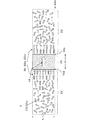
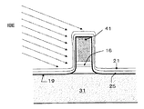
まず、図1および図2を参照して、磁気抵抗素子を備える磁気センサ積層体の構造について説明する。図1は、本実施形態に係る磁気センサ積層体を模式的に示す概略図である。図2は、本実施形態に係る磁気センサ積層体の積層方向に対して垂直なプロフィールを示す概略図である。
<First Embodiment>
[Structure of magnetic sensor laminate]
First, with reference to FIG. 1 and FIG. 2, the structure of the magnetic sensor laminated body provided with a magnetoresistive element is demonstrated. FIG. 1 is a schematic view schematically showing a magnetic sensor laminate according to the present embodiment. FIG. 2 is a schematic diagram illustrating a profile perpendicular to the stacking direction of the magnetic sensor stack according to the present embodiment.
図1に示すように、本実施形態に係る磁気センサ積層体1は、基板31上の略中央部に、組成が異なる複数の積層膜からなり、磁界が印加されることで電気抵抗値が変動する磁気抵抗効果を有する磁気抵抗素子(リーダースタック)10を備える。また、磁気センサ積層体1は、上記リーダースタック10の対向する2つの接合壁面10a、10bの側方のフィールド領域22に、バイアス磁界を上記リーダースタック10に付与することができるハードバイアス積層体20を備えている。このように磁気センサ積層体は、基板31上に、単一の又は複数のリーダースタック10およびハードバイアス積層体20を備えており、ハードディスクドライブ等の磁気読み取りヘッド用のセンサを切り分ける前の中間製品である。
As shown in FIG. 1, the
図1に例示するリーダースタック10は、フリー層16の真下に酸化物バリア層(MgO)を備える磁気トンネル接合体(MTJ)である。これに限定されず、リーダースタック10は、非常に低い抵抗を有する大部分が金属製の巨大磁気抵抗接合体(GMR)であってもよい。
The
具体的には、リーダースタック10は、例えば、NiFe等の軟磁性体からなるボトムシールド層(基板)31上に積層され、主に、反強磁性層である反強磁性ピニング層(AFM層)13、シンセティックアンチフェロ層(SAF層)14、スペーサ層15、および強磁性フリー層16を備えている。
Specifically, the
AFM層13は、例えば、IrMn等の反強磁性体によって形成されている。AFM層13は、例えば、上記ボトムシールド層31上に、必要に応じて不図示のTa等からなるプレシード層およびRu等からなる第3のシード層を介して積層される。
The
SAF層14は、薄いカップリング層(非磁性層またはトンネル絶縁体層)14bを介して、逆向きに結合した2つの強磁性体層14a、14cからなる。SAF層14の強磁性体層は、AFM層13と接触しているピンド層14aと、カップリング層14bと接触しているリファレンス層14cとから構成される。
The
スペーサ層15は、非磁性層またはトンネル絶縁体層からなり、例えば、MgO等の酸化物層により形成されている。
The
フリー層16は、例えば、CoFeB等の強磁性体によって形成されており、CoFeB等の強磁性体層上にTa層、NiFe層を積層した層でもよい。フリー層16は、バイアス磁界がかけられ、リファレンス層14cと直角を成すように配向される。この配置により、センサ感度を高くでき、記憶媒体からの外部磁場に対する線形応答を提供する。バイアス磁界は、「ハードバイアス」とも称され、ディスクドライブの寿命を通して一定に維持されることが期待される。またハードバイアスは、フリー層16に磁区が形成されることを防ぐ。リーダースタック10を通じた磁気抵抗変化は、リファレンス層14cとフリー層16との間の磁化の相対的方向によって決まる。
The
フリー層16は、必要に応じて、例えば、Cr、Ru、Ta、Tiおよびこれらの合金群ならびにCなどから選択される不図示の第3のキャッピング層(図6の17)で覆われている。
The
ここで、少なくとも、ピンド層14a、スペーサ層15、およびフリー層16の接合体が強磁性スタック(FMスタック)18である。FMスタック18には、不図示の第3のキャッピング層(図6の17)を含んでいる場合もある。本実施形態のリーダースタック10は、AFM層13上の一部にFMスタック18を備え、その接合壁面10a、10bが対向する方向(紙面に平行な方向)に沿ったFMスタック18の最上面の幅wFは、同方向に沿ったAFM層13の最上面の幅wAよりも小さく設定されている。すなわち、リーダースタック10は、例えば、断面が幅広の台形状のAFM層13の上に、これより幅の小さい台形状のFMスタック18を積層したような段形状に形成されている。磁気センサ積層体1を、紙面に平行な面で切り分けて、ストライプ高さ(図1では奥行き)hの磁気読み取りヘッド用センサとした場合に、FMスタック18の最上面の幅wFは、ヘッド幅となるため20nm〜30nmであることが好ましい。また、AFM層13の最上面の幅wAは、FMスタック18の最上面の幅wFの2.5倍以下であることが好ましい。wAがwFの2.5倍を超えると、フィールド領域22が減少し、バイアス磁界をリーダースタック10に十分に与えられない可能性がある。
Here, at least the joined body of the pinned
上述したように、基板31上のフィールド領域22にはハードバイアス積層体20が成膜され、このハードバイアス積層体20は、結晶c軸を有する磁性粒を備えた第1および第2の磁性層22a、22bを含んでいる。第1の磁性層22aはリーダースタック10の接合壁面10a、10bに接するように積層され、第2の磁性層22bは第1の磁性層22a上に積層されている。
As described above, the
第1の磁性層22aならびに第2の磁性層22bは、例えば、Co−Pt、Co−Cr−Ptおよびこれらの合金群から選択される六方晶構造(hcp)を有する合金(永久磁石)によって形成されている。これに限定されず、第1の磁性層22aは、Fe−Pt、Co−Ptおよびこれらの合金群から選択される面心正方晶構造(fct)の合金によって形成してもよい。
The first
図1および図2を参照して、第1の磁性層22aならびに第2の磁性層22bの結晶c軸方向(すなわち、結晶粒磁化軸)について説明する。なお、図2中のABSは浮上面を示し、hF、hAは、それぞれFMスタック18、AFM層13のストライプ高さ(図1では奥行き)を示しており、hF=hAである。図2におけるリーダースタック10のフリー層16上の矢印は、ハードバイアス積層体20によるバイアス磁界の付与により、例えば、フリー層16が右方へ磁化された状態を示している。
With reference to FIGS. 1 and 2, the crystal c-axis direction (that is, the crystal grain magnetization axis) of the first
交換結合の存在によって、隣接する磁化は互いにより平行に方向付けられる。本実施形態の磁気センサ積層体1では、リーダースタック10から離れたフィールド領域22において、第2の磁性層22bにおける結晶c軸方向(すなわち、結晶粒磁化軸)は膜面内で2次元(2D)ランダムに分布される。他方、リーダースタック10の接合壁面10a、10bの段形状部分では、FMスタック18の壁近傍の第1の磁性層22aだけでなく、AFM層13の壁上の第1の磁性層22aの結晶c軸は1次元配向(1D1)となる。この方向は、膜面内でABS面に平行であり、接合壁面10a、10bに対して略垂直となる。AFM層壁上の第1の磁性層22aの上にも第2の磁性層22bが積層されているが、第1の磁性層22a上で第2の磁性層22bがエピタキシャル成長するため、第1の磁性層22a上の第2の磁性層22bもまた一次元(1D2)に整列している。
Due to the presence of exchange coupling, adjacent magnetizations are oriented more parallel to each other. In the
フィールド領域22の下部およびリーダースタック10の接合壁面10a、10bの上には、例えば、Al2O3等からなる絶縁層19が配置されている。この絶縁層は、接合壁面において厚さ2〜5nmを有する。
An insulating
第1の磁性層22aおよび第2の磁性層22bは、基板31としてのボトムシールド層上に、上記絶縁層19および必要に応じて下地層21を介して積層される。この下地層21は、例えば、Cr、Cr−Mo、Cr−Ti、Nb、Ta、Wおよびこれらの合金群から選択される体心立方晶構造(bcc)の合金によって形成されている。この下地層21は、例えば、フィールド領域において3〜8nm、接合壁面において3nm未満の厚さを有する。
The first
上記下地層21に加え、この下地層21上にさらに不図示の第1のシード層を備えて、下地層を二重に構成してもよい。即ち、フィールド領域22およびリーダースタック10の接合壁面10a、10bは、例えば、CrB、CrTiB、MgO、Ru、Ta、Ti、およびこれらの合金群から選択される第1のシード層をさらに備えていてもよい。この第1のシード層は、例えば、フィールド領域において厚さ1nm未満、接合壁面において厚さ0.5〜2nmを有する。
In addition to the
また、フィールド領域22および接合壁面10a、10bは、必要に応じて、例えば、Cr、Ru、Ta、Tiおよびこれらの合金群ならびにCから選択される第1のキャッピング層23で覆われている。
Further, the
そして、磁気センサ積層体1は、上記絶縁層19の下にボトムシールド層31を備え、上記第1のキャッピング層23の上にトップシールド層32を備えている。これらシールド層31、32は、例えば、NiFe等の軟磁性体によって形成されている。すなわち、リーダースタック10およびフィールド領域22は、2つの厚い軟磁性シールド層31、32の間に挟まれている。これらシールド層31、32の間がリードギャップ(RG)となる。
The
〔磁気センサ積層体の成膜方法〕
次に、図3から図9を参照して、上記磁気センサ積層体1の作用を説明すると共に、本実施形態に係る磁気センサ積層体1の成膜方法について説明する。
[Method for depositing magnetic sensor laminate]
Next, with reference to FIG. 3 to FIG. 9, the operation of the
図3は、本実施形態に係る磁気センサ積層体1の成膜方法の手順を示す手順図である。本実施形態に係る磁気センサ積層体1の成膜方法は、図3に示すように、まず、基板31上に、少なくとも、AFM層13およびFMスタック18を備えるリーダースタック10を成膜する手順(ステップ1;以下、「S1」のように表記する)を有する。次に、リーダースタック10上にフォトレジストマスク(PR)41のパターンを形成する手順(S2)と、AFM層13の厚さに略等しい厚さのFMスタック18の一部をエッチングする手順(S3)と、を有する。さらに、フォトレジストマスク41の幅をトリミングする手順(S4)と、トリミングしたフォトレジストマスク41aを使用してFMスタック18およびAFM層13をエッチングする手順(S5)と、を有する。そして、絶縁層19を成膜する手順(S6)と、フィールド領域22にハードバイアス積層体20を積層する手順(S7)と、表面を平坦化する手順(S8)と、第2のキャッピング層24およびトップシールド層32を成膜する手順(S9)と、を有する。
FIG. 3 is a procedure diagram showing a procedure of the film forming method of the
さらに、上記フィールド領域22にハードバイアス積層体20を積層する手順(S7)は、基板31の法線から成膜角度θ1(θ1=0〜25度)で、下地層21を成膜する第1の手順(S11)を有する。また、基板31の法線から成膜角度θ2(θ2=50〜90度、好ましくは50〜80度)で、第1の磁性層22aを成膜する第2の手順(S12)を有する。さらに、基板31の法線から成膜角度θ3(θ3=0〜25度)で、第2の磁性層22bを成膜する第3の手順(S13)を有する。そして、基板31の法線から成膜角度θ4(θ4=0〜45度)で、第1のキャッピング層23を成膜する第4の手順(S14)を有する。
Further, in the step (S7) of stacking the hard bias stack 20 in the
さらに、図4および図5を参照して、本実施形態に係る磁気センサ積層体1の成膜方法を具体的に説明する。図4および図5は、磁気センサ積層体1の具体的な成膜方法を示す説明図である。
Furthermore, with reference to FIG. 4 and FIG. 5, the film-forming method of the magnetic sensor laminated
磁気センサ積層体1の作成は、図4(a)に示すように、まず、基板31上に、リーダースタック10となるAFM層13およびFMスタック18を成膜する。基板31としては、例えば、NiFe等の軟磁性体からなるボトムシールド層を採用する。AFM層13は、上述したように、例えば、IrMn等の反強磁性体によって形成され、必要に応じて、Ta等からなるプレシード層およびRu等からなる第3のシード層を介して積層される。FMスタック18は、少なくとも、SAF層14、スペーサ層15、およびフリー層16等から形成され(図1参照)、必要に応じて、例えば、Cr、Ru、Ta、Tiおよびこれらの合金群ならびにCから選択される不図示の第3のキャッピング層(図6の17)で覆われている。
As shown in FIG. 4A, first, the
次に、FMスタック18上に、フォトレジスト(PR)マスク41の塗布、パターニング、及び現像を行なう。フォトレジストマスク41は、後述するエッチング処理に際して、FMスタック18の一部をマスクするためにある。後述する段形状のリーダースタック10におけるAFM層13の幅WAは、主にこのフォトレジストマスク41の幅寸法によって決定される。
Next, a photoresist (PR) mask 41 is applied, patterned, and developed on the
次に、図4(b)に示すように、上記フォトレジストマスク41で覆った部分以外のFMスタック18の表面側をエッチング除去し、AFM層13の厚さに略等しい厚さでエッチングを停止する。エッチング処理には、例えば、イオンビームエッチング(IBE)または反応性イオンエッチング(RIE)等が採用される。しかしながら、IBEでは、エッチングされた材料がフォトレジストマスク41壁に再蒸着することによって、後述するフォトレジストマスク41のトリミングが困難になるため、無酸素RIEによってエッチングすることが好ましい。
Next, as shown in FIG. 4B, the surface side of the
その後、図4(c)に示すように、例えば、プラズマ酸素プロセスなどを用いて、FMスタックの幅WAを決定する幅まで縮小するように、FMスタック18上のフォトレジストマスク41の幅寸法をトリミングする。このトリミングしたフォトレジストマスク41aは、AFM層13およびFMスタック18をエッチングするためのマスクとして利用される。
Thereafter, as shown in FIG. 4C, the width dimension of the
次に、図4(d)に示すように、上記トリミングマスク41aで覆った以外の部分のFMスタック18およびAFM層13をエッチングして除去する。エッチング処理には、上述したと同様に、例えば、イオンビームエッチング(IBE)または反応性イオンエッチング(RIE)等が採用される。エッチングは、ボトムシールド面で停止され、AFM層13上の一部にFMスタック18を備え、接合壁面10a、10bが対向する方向に沿ったFMスタック18の最上面の幅wFが同方向に沿ったAFM層13の最上面の幅wAよりも小さく形成された段形状のリーダースタック10が形成される。
Next, as shown in FIG. 4D, portions of the
エッチング処理の後、図5(e)に示すように、段形状のリーダースタック10が形成された基板31(トリミングマスク41aを含むリーダースタック10およびその接合壁面10a、10bの側方)の上に、絶縁層19を被覆する。絶縁層19は、センサに電流が通るのを制限するために成膜され、例えば、アルミナ(Al2O3)、シリカ(SiO2)等の酸化物、あるいはSi3N4等の窒化物などが好ましい。絶縁層19の成膜は、例えば、物理気相成長法(PVD)、イオンビーム蒸着法(IBD)、原子層蒸着法(ALD)および化学気相成長法(CVD)のいずれかの成膜法が用いられる。ALD法やCVD法ではコンフォーマルな成膜が可能である利点を有する。
After the etching process, as shown in FIG. 5E, on the
次に、上記絶縁層19の上に、ハードバイアス積層体20を成膜する。基本的なハードバイアス積層体20の場合、まず上記絶縁層19上に下地層21を成膜し、次いで磁性層22a、22bおよび第1のキャッピング層23を成膜する。下地層21には、例えば、CrもしくはWおよびこれらの合金などが好ましい。この下地層21の成膜は、例えば、IBD、またはイオン化PVDもしくはコリメートPVDなどによって、基板31面に対して略垂直な角度(基板31の法線からの角度、即ち成膜角度θ1=0〜25度)で行われるのが好ましい。下地層21の大部分は、フィールド領域22および段形状のリーダースタックの水平面上に堆積される。
Next, a
次に、図5(f)に示すように、斜め成膜(基板31の法線からの角度、即ち成膜角度θ2=成膜角度50〜90度、好ましくは50〜80度)で、第1の磁性層22aを成膜する。この第1の磁性層22aの大部分は、結晶c軸が接合壁面10a、10bに対して略垂直に整列した状態で、接合壁面10a、10bおよびその近傍のフィールド領域22上に成膜される。
Next, as shown in FIG. 5 (f), in oblique film formation (angle from the normal line of the
さらに、図5(g)に示すように、第1の磁性層22a上に第2の磁性層22bを成膜する。第2の磁性層22bの成膜は、例えば、IBD、またはイオン化PVDもしくはコリメートPVD等を用いて、基板31面に対して略垂直角度(基板31の法線からの角度、即ち成膜角度θ3=0〜25度)で行われる。その後、第1および第2の磁性層22a、22bを保護するため、あるいはエッチング停止層もしくは化学的機械研磨(CMP)停止層として、第2の磁性層22b上に第1のキャッピング層23が、基板31面に対して略垂直角度(基板31の法線からの角度、即ち成膜角度θ4=0〜45度)で成膜される。
Further, as shown in FIG. 5G, a second
そして、図5(h)に示すように、第1のキャッピング層の成膜後、CMPまたは鋭角イオンビームエッチング(IBE)などによって、図5(g)中の破線で表面を平坦化する。そして、第2のキャッピング層24を成膜した後、トップシールド32を形成する。
Then, as shown in FIG. 5H, after the first capping layer is formed, the surface is flattened by a broken line in FIG. 5G by CMP, acute angle ion beam etching (IBE), or the like. Then, after the
図6は、本実施形態に係る磁気センサ積層体1の完成形を模式的に示す概略図である。上述したように、この磁気センサ積層体1のリーダースタック10は段形状に形成され、第1段はAFM層13によって形成され、第2段はAFM層13よりも幅の小さいFMスタック18によって形成されている。ハードバイアス積層体20の段形状の接合壁面10a、10bに接する部分も、対応する段形状を有している。このハードバイアス積層体20の段形状部分では、FMスタック18の壁近傍の第1の磁性層22aだけでなく、AFM層13の壁上の第1の磁性層22aの結晶c軸も接合壁面10a、10bに対して略垂直に一次元(1D1)で整列している。さらに、AFM層壁上の第1の磁性層22a上で第2の磁性層22bがエピタキシャル成長するために、この一次元(1D1)第1の磁性層22a上の第2の磁性層22bも一次元(1D2)に整列する。これら一次元(1D1、1D2)に整列した磁性層は、リーダースタック10から離れた第2の磁性層22bからの磁束をフリー層へ集束させる機能を有する。したがって、フィールド領域22のうちリーダースタック10近傍で上記一次元(1D1、1D2)磁性層のc軸が配向されため、バイアス効率が結晶粒径にあまり依存しないようになる。さらに、フリー層16の端部の接合壁面にある局所磁界は、ストライプ高さ(奥行き)を減少した場合でも、より均一になる傾向がある。すなわち、段形状のリーダースタック10と第1の磁性層22aの斜め成膜とを利用して、一次元領域を拡張することができる。
FIG. 6 is a schematic view schematically showing a completed form of the
上述した磁性の配向は、図17に例示した様なIBDやPVD等によって達成される。しかし、大きい基板(ウエハ;5〜8インチ)の場合、成膜の入射角が基板31面に対して鋭角であるため、CoPt成膜の初期の段階でInBoard−OutBoard差(リーダースタックに対して基板中心方向側と基板外周側における膜厚の差)が発生する。
The magnetic orientation described above is achieved by IBD, PVD or the like as illustrated in FIG. However, in the case of a large substrate (wafer; 5 to 8 inches), since the incident angle of film formation is acute with respect to the surface of the
そこで、本実施形態の成膜方法では、図7および図8に示すような成膜装置を用いる。図7は、本実施形態の成膜方法に用いる成膜装置を模式的に示す概略図である。図8は、本実施形態の成膜方法に用いる成膜装置を模式的に示す斜視図である。 Therefore, in the film forming method of the present embodiment, a film forming apparatus as shown in FIGS. 7 and 8 is used. FIG. 7 is a schematic view schematically showing a film forming apparatus used in the film forming method of the present embodiment. FIG. 8 is a perspective view schematically showing a film forming apparatus used in the film forming method of the present embodiment.
図7および図8に示すように、この成膜装置51は、例えば、IBD法によって基板ホルダ52上に保持された基板31上に膜を形成する装置であり、斜めに保持されたターゲットTの前方にスリットシャッタ53が配置されている。基板ホルダ52は、不図示の直線移動手段を備え、シャッタ53のスリット54に対して直交するように直線的に移動可能となっている。そして、この成膜装置51は、リーダースタック10の接合壁面と平行な細長い不図示の矩形カソードマグネットを備えている。
As shown in FIGS. 7 and 8, the
このような成膜装置51を用いて、基板31を図7の紙面と直角を成す長手ターゲットTの下で一定の速度で移動または走査する。図8に示すように、リーダースタック10の接合壁面が、長手ターゲットに対して平行となるように配置された状態となっている。すなわち、リーダースタック10の接合壁面10a、10bは、図8中のy軸方向に沿っており、例えば点線A,B,B’C,C’で示されるように、ターゲットTからx軸方向に沿ってスパッタ照射されることになる。
Using such a
上記図4(d)に示すように、段形状のリーダースタック10の接合壁面10a、10bの両側にハードバイアス積層体20を成膜するための2つのフィールド領域22が設けられている。このようなパターンが多数同様のレイアウトで基板31上に平行に形成される。即ち、基板上に複数のリーダースタック10が配置され、各リーダースタック10の両側にあるフィールド領域22に同一の工程でハードバイアス積層体を積層する。
As shown in FIG. 4D, two
下地層21は、まず基板31面に対して略垂直入射で成膜される。殆どの成膜はフィールド領域22上になされ、リーダースタック10およびフォトレジストマスク41aの壁上では非常に薄い層となる。第1の磁性層22aは2つの手順で形成される。
The
第1の手順は、端から端まで成膜されるまで、基板31をターゲットTの下で一定の速度で移動させながら、リーダースタック10の一方の接合壁面10a(または10b)上に基板31面に対して鋭角で成膜する。続いて第2の手順は、基板31を180度回転させ、スパッタ磁束の下で移動させて、同じ角度でもう一方の接合壁面10b(または10a)上に成膜ができるようにする。最少通過回数は2回であるが、両側の最終的な厚さ(15〜40nm)が同じである限り、通過(往復)回数は増加させてもよい。
In the first procedure, the
第2の磁性層22bは基板31面に対して略垂直角度で成膜し、入射角度以外は第1の磁性層22aと同じ方法で形成することができる。第1のキャッピング層(例えば、Ta)は、第2の磁性層22bと同様にして形成される。このTaは、接合壁面10a,10bまたはフォトレジストマスク壁上よりもフィールド領域22上に、より多く成膜される。
The second
下地層21、第2の磁性層22b、および第1のキャッピング層23は、現行のIBDまたは周波数60MHzのRFスパッタを用いたイオン化PVDによって成膜することができる。しかし、第1の磁性層22aは、図7の成膜装置51を用いて、上記の矩形ターゲットTを用いた方法で成膜する。
The
本実施形態では第1の磁性層22aとして、最も一般的に用いられる合金のCo−Ptを用いている。Fe−Ptなどの他の材料も、接合壁面上の面心正方晶構造を用いて成長させてよいが、200℃以上の温度が必要であると考えられる。この場合、センサ積層体の形成にハードマスクとRIE(リアクティブイオンエッチング)を用いれば、ハードバイアス積層体の成膜時にはフォトレジストマスク41aは無くなっており、好適である。
In the present embodiment, the most commonly used alloy Co—Pt is used as the first
Co−Pt(0001)格子面は、MgO(001)格子面またはCr(002)格子面上に成長させることができる。つまり、接合壁面に対してc軸(磁気異方性の方向)を略垂直方向に形成できる。 The Co—Pt (0001) lattice plane can be grown on the MgO (001) lattice plane or the Cr (002) lattice plane. That is, the c-axis (magnetic anisotropy direction) can be formed in a substantially vertical direction with respect to the bonding wall surface.
なお、これは基板31上の全てのリーダースタック10が、全て平行であるようにパターニングされていると仮定している。また、リーダースタック10の接合壁面は、成膜の間、図8に示されるように矩形ターゲットTと平行に保持される。
This assumes that all the reader stacks 10 on the
即ち、第1の磁性層22aの成膜は、上記ターゲットTの下で、基板31を一定の速度で直線的に移動させて、リーダースタック10の接合壁面10a、10bの一方の面を成膜するステップを有する。次いで、基板31をその中央垂直軸を中心に180度回転させ、上記ターゲットTの下で基板31を一定の速度で直線的に移動させて、上記接合壁面10a、10bの他方の面を成膜するステップを有する。
That is, the first
一方、上述したように、下地層21、第2の磁性層22bおよび第1のキャッピング層23の成膜は、第1の磁性層22aと成膜角度(スパッタ粒子などの入射角)が異なっている。しかし、下地層21、第2の磁性層22bおよび第1のキャッピング層23の場合にも、上記ターゲットTの下で、基板31を一定の速度で直線的に移動させて、一方のフィールド領域22に成膜するステップを有する。次いで、基板31をその中央垂直軸を中心に180度回転させ、上記ターゲットTの下で、基板31を一定の速度で直線的に移動させて、他方のフィールド領域22に成膜するステップを有する。
On the other hand, as described above, the film formation of the
上記各手順およびフィールド領域の積層手順における成膜方法のアルゴリズムは、例えば、IBDシステムの不図示の制御系に備えられたHDDやROM等の記録装置に成膜制御プログラムとしてインストールされ、CPUによって適宜読み出されて実行される。 The algorithm of the film formation method in each of the above procedures and the field region stacking procedure is installed as a film formation control program in a recording device such as an HDD or a ROM provided in a control system (not shown) of the IBD system, and is appropriately executed by the CPU It is read and executed.
記録媒体は、コンピュータによる読み取り可能な可搬性の記録媒体であり、記録媒体に記録された成膜制御プログラムは上記記憶装置にインストールされる。記録媒体としては、コンパクトフラッシュ(登録商標)、スマートメディア(登録商標)、メモリースティック(登録商標)、マルチメディアカード、SDメモリカード等のフラッシュメモリ系が挙げられる。また、マイクロドライブ(登録商標)等のリムーバブルハードディスク系、フロッピー(登録商標)ディスク等の磁気記録系が挙げられる。さらに、MO等の光磁気記録系、CD−R、DVD−R、DVD+R、DVD−RAM、DVD+RW(登録商標)、PD等の光ディスク等が挙げられる。 The recording medium is a computer-readable portable recording medium, and the film formation control program recorded on the recording medium is installed in the storage device. Examples of the recording medium include flash memory systems such as compact flash (registered trademark), smart media (registered trademark), memory stick (registered trademark), multimedia card, and SD memory card. In addition, a removable hard disk system such as a microdrive (registered trademark) and a magnetic recording system such as a floppy (registered trademark) disk can be used. Further, magneto-optical recording systems such as MO, optical disks such as CD-R, DVD-R, DVD + R, DVD-RAM, DVD + RW (registered trademark), PD, and the like can be mentioned.
次に、磁気センサ積層体1における磁気抵抗素子10のAFM層13を所定の範囲に区画して、第1の本発明を適用しない例と比較して、第1の本発明の作用効果を検討する。
Next, the
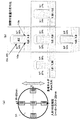
図9(a)は、比較例として作成した磁気抵抗素子のAFM層およびその結晶粒の概略図である。図9(a)に示した磁気抵抗素子は、FMスタックの幅wF=AFM層の幅wA=80nm、FMスタックのストライプ高さhF=AFM層のストライプ高さhA=80nmである。図9(a)に示すように、80nm×80nmの範囲内では、AFM層13は10個の結晶粒からなる。これらの結晶粒の殆どはその寸法によって、また互いの交換結合によって安定している。磁気抵抗素子の寸法が、点線で示す30nm(幅wF、wA)×40nm(ストライプ高さhF、hA)まで減少すると、FMスタックの下方のAFM層13の結晶粒は7個の結晶粒まで減少し、そのうちの5個(灰色で影が付けられた結晶粒)は寸法が小さくなったために熱的に不安定である。
FIG. 9A is a schematic diagram of an AFM layer and crystal grains of a magnetoresistive element prepared as a comparative example. The magnetoresistive element shown in FIG. 9A has FM stack width w F = AFM layer width w A = 80 nm, FM stack stripe height h F = AFM layer stripe height h A = 80 nm. . As shown in FIG. 9A, the
図9(b)は、本実施形態の磁気抵抗素子のAFM層およびその結晶粒の概略図である。図9(b)に示すように、FMスタック18は図9(a)のものと同じ寸法(30nm(幅wF)×40nm(ストライプ高さhF)まで小さくなったが、AFM層13は磁気抵抗素子の幅方向に沿って延びている状態、即ち、AFM層13の寸法は80nm(幅wA)×40nm(ストライプ高さhA)である状態を示している。FMスタック18の下方における1個の結晶粒(灰色で影が付けられた結晶粒)だけが潜在的に不安定である。したがって、AFM層13の幅wAを拡張することによって、熱的安定性が著しく向上する。
FIG. 9B is a schematic view of the AFM layer and crystal grains of the magnetoresistive element of this embodiment. As shown in FIG. 9B, the
以上説明したように、本実施形態の磁気センサ積層体1およびその成膜方法等によれば、多層構造のFMスタック18の幅wFが、AFM層13の幅wAよりも小さい段形状のリーダースタック10を備えている。したがって、TPIが増大し、かつFMスタック18の幅wFが減少したことにより、熱的に誘発される不安定性を防止すべく、AFM層13の幅wAが維持されるか、あるいはより広く設計される。しかし、段形状のAFM層13及びFMスタック18によって、接合壁面10a、10bの近傍からフィールド領域22へ延びる第1の磁性層22aが、AFM層13と多層構造のFMスタック18の幅の差に応じて薄くなる。
As described above, according to the
リーダースタック両側の接合壁面10a、10b近傍に成膜された第1の磁性層22aおよび第2の磁性層22bの結晶c軸は、ABS面に沿っており、接合壁面10a、10bに対して略垂直方向に配向するという優れた効果を奏する。すなわち、接合壁面付近のc軸は一次元(1D1、1D2)整列されており、バイアス磁界をフリー層16へ効果的に集中させる。一次元(1D1、1D2)の磁性層部分は、AFM層13の幅wAを超えて延びている。これに対してリーダースタック両側の接合壁面10a、10bから離れているフィールド領域22における第2の磁性層22bのc軸は二次元(2D)ランダムである。この接合壁面10a、10bから離れた領域の第2の磁性層22bは、第1のシード層および下地層の斜め入射(>50度)成膜によりわずかにORが上がると思われるが、必ずしも磁性層の斜め成膜によって生じたのではない。
The crystal c-axes of the first
<第2の実施形態>
次に、図10および図11を参照して、第2の実施形態の磁気センサ積層体100およびその成膜方法について説明する。図10は、第1の実施形態の図5(f)(g)に相当する手順の概略図である。図11は、本実施形態による磁気センサ積層体の完成形を示す概略図である。なお、第1の実施形態と同一構成の部材については、同一の符号を付して説明する。
<Second Embodiment>
Next, with reference to FIG. 10 and FIG. 11, the magnetic sensor laminated
図10におけるハードバイアス積層体20は、従来の成膜方法、すなわち、基板31面に対して略垂直な角度で成膜されたものである。磁性層122は、FMスタック18よりも幅広のAFM層13の上方で突出して形成される。図10中の破線の上方のハードバイアス積層体20の一部が、平坦化処理によって除去される。
The
この平坦化処理の後に磁性層122が空気にさらされるのを防止するため、不図示の統合的な全真空の成膜装置で行なうことが好ましい。この成膜装置は、ウェハ処理用ロボットを有する中央真空モジュールを備え、この中央真空モジュールにBEおよびPVDのモジュールを備える。
In order to prevent the
平坦化処理は、基板31を回転させながら鋭角でエッチングすることによって行われる。その後、露出された磁性層122およびFMスタック18は、PVDモジュールの中で第2のキャッピング層24を被覆する。この第2のキャッピング層24は保護層として機能し、またトップシールド層32を積層するためのシード層としても機能する。平坦化処理はCMPプロセスを含んでもよい。また、第2のキャッピング層24およびトップシールド層32の成膜前に、酸化した磁性層122の表面をエッチングしてもよい。
The flattening process is performed by etching at an acute angle while rotating the
図11に示すように、第1の実施形態と同様に、本実施形態のリーダースタック10は、AFM層13上の一部にFMスタック18を備え、その接合壁面10a、10bが対向する方向に沿ったFMスタック18の最上面の幅wFは、同方向に沿ったAFM層13の最上面の幅wAよりも小さく設定されている。すなわち、リーダースタック10は、例えば、断面が幅広の台形状のAFM層13の上に、これより幅の狭い台形状のFMスタック18を積層したような段形状に形成されている。
As shown in FIG. 11, as in the first embodiment, the
本実施形態では、上記接合壁面10a、10b近傍の磁性層122のc軸は、ABS面に沿って配向されている。すなわち、上記接合壁面10a、10b近傍の磁性層122のc軸は、AFM層13およびFMスタック18の接合壁面10a、10bの双方に対して略垂直であり、一次元(1D)に整列されて、バイアス磁界をフリー層16へ効果的に集中させる。この一次元(1D)の磁性層部分は、AFM層13の幅wAを越えて延びている。これに対して、上記接合壁面10a、10bから離れているフィールド領域22における磁性層122のc軸は二次元(2D)ランダムである。したがって、本実施形態による磁気センサ積層体100は、基本的に第1の実施形態と同様の作用効果を奏する。
In the present embodiment, the c-axis of the
<第3の実施形態(参考形態)>
〔磁気センサ積層体の構造〕
まず、図12および図13を参照して、磁気抵抗素子を備える磁気センサ積層体の構造について説明する。図12は、本実施形態に係る磁気センサ積層体を模式的に示す概略図である。図13は、本実施形態に係る磁気センサ積層体の積層方向に対して垂直なプロフィールを示す概略図である。
<Third embodiment (reference form) >
[Structure of magnetic sensor laminate]
First, with reference to FIG. 12 and FIG. 13, the structure of the magnetic sensor laminated body provided with a magnetoresistive element is demonstrated. FIG. 12 is a schematic view schematically showing the magnetic sensor laminate according to the present embodiment. FIG. 13 is a schematic diagram showing a profile perpendicular to the stacking direction of the magnetic sensor stack according to this embodiment.
図12に示すように、本実施形態に係る磁気センサ積層体1は、基板31上の略中央部に、組成が異なる複数の積層膜からなり、磁界が印加されることで電気抵抗値が変動する磁気抵抗効果を有する磁気抵抗素子(リーダースタック)10を備える。また、磁気センサ積層体1は、上記リーダースタック10の対向する2つの接合壁面10a、10bの側方のフィールド領域22に、バイアス磁界を上記リーダースタック10に付与するハードバイアス積層体20を備えている。このように磁気センサ積層体1は、基板31上に、単一の又は複数のリーダースタック10およびハードバイアス積層体20を備えており、ハードディスクドライブ(HDD)等の磁気読み取りヘッド用のセンサを切り分ける前の中間製品である。
As shown in FIG. 12, the
図12に例示するリーダースタック10は、フリー層16の真下に酸化物バリア層(MgO)を備える磁気トンネル接合体(MTJ)である。これに限定されず、リーダースタック10は、低い抵抗を有する面直電流(CPP)型の巨大磁気抵抗接合体(GMR)であってもよい。
The
具体的には、リーダースタック10は、例えば、NiFe等の軟磁性体からなるボトムシールド層(基板)31上に積層され、主に、反強磁性層である反強磁性ピニング層(AFM層)13、シンセティックアンチフェロ層(SAF層)14、スペーサ層15、および強磁性フリー層16を備えている。
Specifically, the
AFM層13は、例えば、IrMn等の反強磁性体によって形成されている。AFM層13は、例えば、上記ボトムシールド層31上に、必要に応じて不図示のTa等からなるプレシード層(図14の11)およびRu等からなる第3のシード層(図14の12)を介して積層される。
The
SAF層14は、薄いカップリング層(非磁性層またはトンネル絶縁体層)14bを介して、逆向きに結合した2つの強磁性体層14a、14cからなる。SAF層14の強磁性体層は、AFM層13と接触しているピンド層14aと、カップリング層14bと接触しているリファレンス層14cとから構成される。
The
スペーサ層15は、非磁性層またはトンネル絶縁体層からなり、例えば、MgO等の酸化物層により形成されている。
The
フリー層16は、例えば、CoFeB等の強磁性体によって形成されており、CoFeB等の強磁性体層上にTa層、NiFe層を積層した層でもよい。フリー層16は、バイアス磁界がかけられ、リファレンス層14cと直角を成すように配向される。この配置により、センサ感度を高くでき、記憶媒体からの外部磁場に対する線形応答を提供する。バイアス磁界は、「ハードバイアス」とも称され、ディスクドライブの寿命を通して一定に維持されることが期待される。またハードバイアスは、フリー層16に磁区が形成されることを防ぐ。リーダースタック10を通じた磁気抵抗変化は、リファレンス層14cとフリー層16との間の磁化の相対的方向によって決まる。
The
フリー層16は、必要に応じて、例えば、Cr、Ru、Ta、Tiおよびこれらの合金群ならびにCなどから選択される不図示の第3のキャッピング層(図14の17a,17b)で覆われている。
The
上述したように、基板31上のフィールド領域22にはハードバイアス積層体20が成膜され、このハードバイアス積層体20は、結晶c軸を有する結晶粒を備えた磁性層26を含んでいる。
As described above, the hard bias stacked
図13に示すように、本実施形態の磁気センサ積層体1では、リーダースタック10から離れたフィールド領域22において、磁性層26のc軸(結晶粒磁化軸)は1次元配向(1D)となる。この磁性層26のc軸の配向は、その膜面内でABS面に沿っており、接合壁面10a、10bに対して略垂直となる。
As shown in FIG. 13, in the
再び図12を参照して、磁性層26は、例えば、Co−Pt、Co−Cr−Ptおよびこれらの合金群から選択される六方晶構造(hcp)を有する合金によって形成されている。磁性層26は、これに限定されず、Fe−Pt、Co−Ptおよびこれらの合金群から選択される面心正方晶構造(fct)の合金によって形成してもよい。
Referring to FIG. 12 again, the
本実施形態では、磁性層26は、ボトムシールド層31上に、少なくとも、下地層21および絶縁層19および介して積層されている。絶縁層19は、必要に応じて、積層される。
In the present embodiment, the
絶縁層19は、フィールド領域22の下部およびリーダースタック10の接合壁面10a、10bの上に配置され、例えば、Al2O3またはSiO2などの酸化物や窒化物等によって形成されている。この絶縁層19は、例えば、フィールド領域22において厚さ2〜10nmの厚さ、接合壁面において厚さ2〜5nmを有する。
The insulating
下地層21は、例えば、W−Ti、RuAl、CrNb、Cr−Ti、Cr−Mo等のCr、Ti、Nb、Ta、W、Ru、Alおよびこれらの合金群から選択される体心立方晶構造(bcc)の合金によって形成されている。この下地層21は、例えば、フィールド領域において3〜8nm、接合壁面において3nm未満の厚さを有する。
The
この下地層21は、絶縁層19上に、第2のシード層25を介して成膜することが好ましい。第2のシード層25は、例えば、Ta−N、Nb−NまたはRuAl−N等の金属窒化物、Co−Wによって形成されている。この第2のシード層25は、例えば、フィールド領域において3〜8nm、接合壁面において3nm未満の厚さを有する。
The
さらに、磁性層26は、必要に応じて、例えば、Cr、Ru、Ta、Tiおよびこれらの合金群ならびにCから選択される第1のキャッピング層23で覆われている。
Furthermore, the
そして、磁気センサ積層体1は、上記絶縁層19の下にボトムシールド層31を備え、上記第1のキャッピング層23の上にトップシールド層32を備えている。これらシールド層31、32は、例えば、NiFe等の軟磁性体によって形成されている。すなわち、リーダースタック10およびハードバイアス積層体20は、2つの厚い軟磁性シールド層31、32の間に挟まれている。これらシールド層31、32の間がリードギャップ(RG)となる。
The
〔磁気センサ積層体の成膜方法〕
次に、図7及び図14から図20を参照して、本実施形態の磁気センサ積層体1の成膜方法を説明すると共に、上記磁気センサ積層体1の作用について説明する。図14は、磁気抵抗素子上にフォトレジストマスクを配置した磁気センサ積層体を示す概略図である。図15は、本実施形態の磁気センサ積層体を構成するハードバイアス積層体をフィールド領域に成膜する手順を示す工程図である。
[Method for depositing magnetic sensor laminate]
Next, with reference to FIG. 7 and FIG. 14 to FIG. 20, the film forming method of the magnetic
図14および図15に示すように、磁気センサ積層体1の作成は、まず基板31上に、リーダースタック10を構成する複数の層を積層する(S21)。基板31としては、例えば、NiFe等の軟磁性体からなるボトムシールド層を採用する。なお、リーダースタック10を構成するAFM層13は、例えば、ボトムシールド層(基板)31上に、必要に応じてTa等からなるプレシード層11およびRu等からなる第3のシード層12を介して積層される。
As shown in FIGS. 14 and 15, the
次に、フォトレジスト(PR)の塗布、パターニング、及び現像を行った後、フォトレジストをマスク41としてエッチング処理して、断面形状が台形状を呈するリーダースタック10を形成する(S22)。フォトレジストマスク41は、エッチング処理に際して、リーダースタック10の一部をマスクするためにある。エッチング処理には、例えば、イオンビームエッチング(IBE)または反応性イオンエッチング(RIE)が採用される。RIEを用いる場合には、リーダースタック構成層上にハードマスクを形成してもよい。この場合、フォトレジストマスク41は最初にハードマスクを形成するために使用され、上記リーダースタック構成層をエッチングする前に、酸素アッシングプロセス等によって除去される。
Next, after applying, patterning, and developing a photoresist (PR), etching is performed using the photoresist as a
エッチング処理の後、フォトレジストマスク41を含むリーダースタック10およびその接合壁面10a、10bの側方の上に、絶縁層19を被覆する(S23)。絶縁層19の被覆には、Al2O3またはSiO2などの酸化物絶縁体(3〜5nm)が好ましく、例えば、物理気相成長法(PVD)、イオンビーム蒸着法(IBD)、原子層蒸着法(ALD)または化学気相成長法(CVD)などの成膜法が用いられる。ALD法やCVD法は、コンフォーマルな成膜が可能である利点を有する。
After the etching process, the insulating
次に、上記絶縁層19の上に、ハードバイアス積層体20を成膜する。本実施形態のハードバイアス積層体20の場合には、上記絶縁層19上に第2のシード層25および下地層21を成膜し(S24及びS25)、次いで磁性層26および第1のキャッピング層23を成膜する(S26)。
Next, a
具体的には、まず、上記絶縁層19上に、基板31の法線から45度を超え90度未満の成膜角度、好ましくは60〜75度の成膜角度で、接合壁面の方向に沿って第2のシード層25を傾斜成膜する(S24)。この第2のシード層25は、例えば、Ta−N等の金属窒化物によって形成され、処理ガス(Ar等)およびN2雰囲気中で反応性成膜してもよく、この場合のN2の部分圧は10〜30%であることが好ましい。あるいは、第2のシード層25は、窒化物ターゲットを用いて成膜してもよい。
Specifically, first, on the insulating
次に、この第2のシード層25上に、基板31の法線からから基板31の法線から45度を超え90度未満の成膜角度、好ましくは50〜70度の成膜角度で、接合壁面の方向に沿って下地層21を傾斜成膜する(S25)。
Next, on this
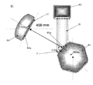
本実施形態では、図7および図16に示すような成膜装置を用いて、第2のシード層25および下地層21の傾斜成膜を行う。図7は、本実施形態の成膜方法に用いる成膜装置を模式的に示す概略図である。図16は、本実施形態の成膜方法に用いる成膜装置を模式的に示す斜視図である。
In the present embodiment, the
図7および図16に示すように、この成膜装置51は、例えば、IBD法によって基板ホルダ52上に保持された基板31上に膜を形成する装置であり、斜めに保持されたターゲットTの前方にスリットシャッタ53が配置されている。基板ホルダ52は、不図示の直線移動手段を備え、シャッタ53のスリット54に対して直交するように直線的に移動可能となっている。このような成膜装置51を用いて、基板31を図7の紙面と直角を成す長手ターゲットTの下で一定の速度で移動または走査する。
As shown in FIG. 7 and FIG. 16, this
図16に示すように、リーダースタック10の接合壁面が、長手ターゲットに対して垂直となるように配置された状態となっている。すなわち、リーダースタック10の接合壁面10a、10bは、図16中のy軸方向に沿っており、例えば点線A,B,B’C,C’で示されるように、ターゲットTからy軸方向に沿ってスパッタ照射されることになる。
As shown in FIG. 16, the joining wall surface of the
このようなリーダースタック10のパターンが多数同様のレイアウトで基板31上に平行に形成されている。すなわち、基板31上に複数のリーダースタック10が配置され、各リーダースタック10の両側にあるフィールド領域22に同一の工程で第2のシード層25および下地層21を成膜する。
Many such patterns of the
この成膜装置51による傾斜成膜は2つの手順で行われる。すなわち、第1の手順は、基板31の端から端まで成膜されるまで、基板31をターゲットTの下で一定の速度で移動させながら、素子接合壁面10a、10bおよびフィールド領域22上に傾斜成膜する。続いて第2の手順は、基板31を180度回転させ、ターゲットTの下で移動させながら、素子接合壁面10a、10bおよびフィールド領域22上に傾斜成膜する。最少通過回数は少なくとも往復の2回であるが、通過(往復)回数は増加させてもよい。このように第2のシード層25および下地層21の成膜を行うことにより、膜厚を均一に成膜することができる。
The inclined film formation by the
そして、下地層21上に、基板31の法線から0〜30度の成膜角度で、磁性層26を成膜する(S26)。本実施形態では、基板31面に対して略垂直に近い角度で磁性層26を成膜するので、図17に示すような現行のイオンビーム蒸着(IBD)システムまたはイオン化PVD装置によって成膜することができる。図17は、IBDシステムの一例を示す概略図である。
Then, the
図17に示すように、このIBDシステム61は、ターゲットTへ向けてイオンビームを照射するビーム照射装置62と、複数のターゲットTを搭載する回転カルーセル63と、基板31を保持する基板ホルダ64と、を備える。
As shown in FIG. 17, this
ビーム照射装置62のイオンビームIBは、電気的にバイアスされたグリッドGによってプラズマ源から引き出され、照射ターゲットTに向けられる。ビームIBを特定の角度に向けることにより、殆どのスパッタ粒子を基板ホルダ64上の基板31に蒸着させることができる。
The ion beam IB of the beam irradiation device 62 is extracted from the plasma source by the electrically biased grid G and directed to the irradiation target T. Most sputtered particles can be deposited on the
回転カルーセル63は、多角形状(例えば、六角形状)を呈し、ターゲット搭載面63aを有しており、これら搭載面63aにターゲットTが搭載される。ターゲット材料としては、例えば、CoPt等が採用される。回転カルーセル63は、イオンビームIBによってスパッタされるターゲット材料が基板31へ向けて対向するように回転する。なお、ターゲット搭載面63aの大きさは、通常、40cm×30cmである。
The rotating
基板ホルダ64は、回転カルーセル63上の照射ターゲットTに対向するステージ64aに基板31を保持する。この基板ホルダ64は、不図示の回転駆動手段により回転可能に構成され、成膜の均一性を向上させるために、蒸着中に基板31を回転させる。また、基板ホルダ64はステージ64aを傾斜させて、照射ターゲットTからの入射粒子に対する基板31の角度を変更することが可能である。
The
なお、基板31から照射ターゲットまでの距離は、例えば、40cmよりも大きくすることができる。この距離が大きくなるほど、入射粒子が平行照射に改善されるが、ターゲットを良好に使用できなくなり、真空チャンバが大きくなる。
In addition, the distance from the board |
次に、磁性層26上に、基板31の法線から0〜30度の基板面に対して略垂直な成膜角度で、第1のキャッピング層23を成膜する(S27)。
Next, the
上述したように、磁性層26および第1のキャッピング層23は基板面に対して略垂直な角度で成膜するので、図17に例示したような現行のIBDやPVD等によって成膜することができる。しかし、大きい基板(5〜8インチ)31の場合には、IB−OB(インボード−アウトボード)の問題が生じ易い。
As described above, since the
そこで、磁性層26および第1のキャッピング層23についても、図7および図8に示したような成膜装置51を用いて往復成膜することにより、IB−OB(インボード−アウトボード)の問題を解消することができる。具体的には、磁性層26および第1のキャッピング層23は、基板31の長手方向に沿った、即ち、図8に示すように前記磁気抵抗素子10の接合壁面と平行な細長いターゲットの下で、基板31を一定の速度で直線的に移動させて、一方のフィールド領域22に成膜する。続いて、基板31をその中央垂直軸を中心に180度回転させ、上記ターゲットの下で、基板31を一定の速度で直線的に移動させて、他方のフィールド領域22に成膜する。
Therefore, the
最後に、リーダースタック10およびハードバイアス積層体20の表面を平滑化処理した後(S28)、上記第1のキャッピング層23上に、例えば、NiFe等の軟磁性体からなるトップシールド層32を配置する。すなわち、リーダースタック10およびハードバイアス積層体20は、2つの厚い軟磁性シールド層31、32で挟まれている。
Finally, after smoothing the surfaces of the
本実施形態の成膜方法のアルゴリズムは、例えば、上記成膜装置51等の不図示の制御系に備えられたハードディスクやROM等の記録装置に成膜制御プログラムとしてインストールされ、CPUによって適宜読み出されて実行される。
For example, the algorithm of the film forming method of the present embodiment is installed as a film forming control program in a recording device such as a hard disk or a ROM provided in a control system (not shown) such as the
記録媒体は、コンピュータによる読み取り可能な可搬性の記録媒体であり、記録媒体に記録された成膜制御プログラムは上記記憶装置にインストールされる。記録媒体としては、コンパクトフラッシュ(登録商標)、スマートメディア(登録商標)、メモリースティック(登録商標)、マルチメディアカード、SDメモリカード等のフラッシュメモリ系が挙げられる。また、マイクロドライブ(登録商標)等のリムーバブルハードディスク系、フロッピー(登録商標)ディスク等の磁気記録系が挙げられる。さらに、MO等の光磁気記録系、CD−R、DVD−R、DVD+R、DVD−RAM、DVD+RW(登録商標)、PD等の光ディスク等が挙げられる。 The recording medium is a computer-readable portable recording medium, and the film formation control program recorded on the recording medium is installed in the storage device. Examples of the recording medium include flash memory systems such as compact flash (registered trademark), smart media (registered trademark), memory stick (registered trademark), multimedia card, and SD memory card. In addition, a removable hard disk system such as a microdrive (registered trademark) and a magnetic recording system such as a floppy (registered trademark) disk can be used. Further, magneto-optical recording systems such as MO, optical disks such as CD-R, DVD-R, DVD + R, DVD-RAM, DVD + RW (registered trademark), PD, and the like can be mentioned.
図18は、ハードバイアス積層体の層構成、およびハードバイアス積層体の磁化ループを示す概略図である。図18において、(a)はハードバイアス積層体の層構成であり、上層から第1のキャッピング層23(WTi)3nm/磁性層26(CoPt)20nm/下地層21(WTi)4nm/第2のシード層25(Ta−N)3,4,5nm/熱酸化膜/基板31(Si)の構成である。(b)は、下地層21(WTi)8nm/基板31(SiO2)上の2次元等方性CoPt磁性層26に対応している。さらに、(c)〜(e)は、(a)に示すWTi/TaN上の配向型の20nm厚のCoPtハードバイアス膜の磁化ループを示している。ここで、磁性層26の膜厚は、10〜30nmである。
FIG. 18 is a schematic diagram illustrating the layer configuration of the hard bias stack and the magnetization loop of the hard bias stack. In FIG. 18, (a) shows the layer structure of the hard bias laminate, from the upper layer to the first capping layer 23 (WTi) 3 nm / magnetic layer 26 (CoPt) 20 nm / underlayer 21 (WTi) 4 nm / second. The seed layer 25 (Ta—N) has a configuration of 3, 4, 5 nm / thermal oxide film / substrate 31 (Si). (B) corresponds to the two-dimensional isotropic CoPt
図18(c)〜(e)に示すように、ORは第2のシード層25の厚さt1(Ta−N)と共に増加するが、僅かに高いHcがt1=4nmに対して観察される。注目すべきは、第2のシード層25と下地層21の合計膜厚が10nm未満であり、磁性層26が基板面に対して略垂直に近い角度で成膜されていても、方形性が向上している。そして、実測値1.6という1.5を超える大きい保磁力配向比(OR値)と、実測値約0.95という0.9を超える角形比がt1=4および5nmに対し観察されることである。なお、磁気異方性が得られた膜において磁化容易軸を測定すると、通常は角形比が1に近づき、逆に磁化困難軸側の角形比は低くなる。
As shown in FIGS. 18C to 18E, OR increases with the thickness t1 (Ta-N) of the
本実施形態では、特により小さい厚さの値でのOR>1となる最良の結果が、Ti組成比が10原子%<Ti<30原子%、好ましくは10原子%であるW−Tiの下地層21について見出された。
In this embodiment, the best result with OR> 1 particularly at smaller thickness values is under W-Ti where the Ti composition ratio is 10 atomic% <Ti <30 atomic%, preferably 10 atomic%. Found for
実質的には、CrTiおよびCrMoのようなCr合金を第2のシード層25として使用すると、ORまたは保磁力Hcは著しく低減する。一方、CrNb(Nbの組成比が約30原子量%)は、媒体用途についてShibamotoらによって報告されているように、ORが1より大きくなり、図18(b)とほぼ同等の磁性ループ形状を示す。
Essentially, the use of a Cr alloy such as CrTi and CrMo as the
次に、本実施形態の成膜方法における結晶成長について、XRD(X線回折装置)測定データ等を用いて検討する。図19は、Ta−N第2のシード層25およびW−Ti下地層21上に成膜されたCoPt磁性層26のXRDスペクトルを示す説明図である。なお、ハードバイアス積層体20の層構成は、上層から第1のキャッピング層23/磁性層26(CoPt)20nm/下地層21(WTi)5nm/第2のシード層25(Ta−N)5nm/熱酸化膜/基板31(Si)の層構成である。また、第2のシード層25(Ta−N)は70度の成膜角度で、下地層21(WTi)は60度の成膜角度で、接合壁面の方向に沿ってそれぞれ傾斜成膜され、磁性層26(CoPt)は基板面31に対して略垂直に近い角度で成膜している。
Next, crystal growth in the film forming method of the present embodiment will be examined using XRD (X-ray diffractometer) measurement data and the like. FIG. 19 is an explanatory diagram showing an XRD spectrum of the CoPt
図19のXRDデータにより、第2のシード層25および下地層21を傾斜成膜して、磁性層(CoPt)26を略垂直に近い角度で成膜しても、磁性層26のc軸が膜面内でABS面に沿って1次元(1D)に配向していることが判る。これは、XRDデータにおいて、Co(100)のピークが確認できることから判断できる。
According to the XRD data in FIG. 19, even if the
一方、図19のCo(002)のピークは基板垂直方向の配向を示すものであるが、測定の特性上から現れるものであり、図18(c)(d)のヒステリシスループを確認することにより、基板垂直方向の配向がないことが判る。これは、基板垂直方向に配向している場合には、図20の点線Lに示すようなヒステリシスループを示すからである。 On the other hand, the peak of Co (002) in FIG. 19 indicates the orientation in the vertical direction of the substrate, but appears from the characteristics of the measurement. By confirming the hysteresis loop in FIGS. It can be seen that there is no orientation in the direction perpendicular to the substrate. This is because the hysteresis loop as shown by the dotted line L in FIG.
以上説明したように、本実施形態によれば、第2のシード層25および下地層21の材質、膜厚、スパッタ入射角の最適化を図ることにより、磁性層26の磁気異方性を高めることができる。このように上記第2のシード層25および下地層21の上に形成された磁性層26は、六方晶構造(hcp)のCo−Pt系合金であって、層内に空隙が存在しない。そして、(10.0)格子面を有し、磁性層26の膜面内で、磁性層26のc軸がABS面に沿って1次元配向(1D)しており、0.9を超える角形比を有している。すなわち、磁性層26の膜面内で、磁性層26のc軸が接合壁面に略垂直方向に配向しているので、磁束をリーダースタック10に集中させることができる。
As described above, according to the present embodiment, the magnetic anisotropy of the
<第4の実施形態(参考形態)>
次に図21を参照して、第4の実施形態の成膜方法に用いる成膜装置について説明する。図21は、本実施形態の成膜装置を模式的に示す概略図である。なお、第3の実施形態と同様の構成要素については同一の符号を付して説明する。
<Fourth embodiment (reference form) >
Next, a film forming apparatus used for the film forming method of the fourth embodiment will be described with reference to FIG. FIG. 21 is a schematic view schematically showing the film forming apparatus of this embodiment. In addition, the same code | symbol is attached | subjected and demonstrated about the component similar to 3rd Embodiment.
図21に示すように、本実施形態の成膜装置71は、ターゲットTを保持するターゲットホルダ72と、このターゲットホルダ72を前面に備えるカソード73と、基板31を保持する基板ホルダ74とを備える。さらに、この成膜装置71は、ターゲットTと基板31との間に、断面が円弧状のシャッタ75を備えており、このシャッタ75はスリット76を有している。
As shown in FIG. 21, the
基板ホルダ74は、その後端側にターゲットTの長手方向に平行な不図示の回動軸を備えており、成膜プロセス中に、この軸周りに基板31をパン(P1)させるようになっている。さらに、この基板ホルダ74は、z1軸を中心として回転可能に構成されている。
The
カソード73は、その後端側にターゲットTの長手方向に平行な不図示の回動軸を備えており、成膜プロセス中に、この軸周りにターゲットTをパン(P2)させるようになっている。基板31のパン(P1)とターゲットTのパン(P2)とは、相反する方向にパニングされる。
The
なお、シャッタ75は、その周方向に沿ってパン(P3)され、成膜プロセスの前後においてスリット76を閉じることが可能である。
The
次に、本実施形態の磁気センサ積層体1の成膜方法について説明する。図22は、本実施形態の成膜方法において、フィールド領域にハードバイアス積層体を成膜する手順を示す工程図である。図23は、本実施形態の成膜装置を用いる場合の成膜状況を示す説明図である。図24は、本実施形態の成膜方法におけるトリミング手順を示す説明図である。
Next, a film forming method of the
図22および図23に示すように、フィールド領域22にハードバイアス積層体20を成膜する工程の具体的手順は、まず、上記成膜装置71を用いて、基板31の法線から45度を超え90度未満の成膜角度、好ましくは60〜75度の成膜角度で、接合壁面の方向に沿って第2のシード層25を傾斜成膜する(S31)。成膜プロセス中に基板31とターゲットTとを相反する方向にパニングするが、パニング中には基板31を回転させない。成膜プロセスの1回のパスの後、基板31はz1軸に沿って180°回転させて、再びパニングする。なお、1回のパスは、スパッタ粒子Sが基板31に対して形成する角度がθから−θまで変化する場合に用いられることもある。
As shown in FIG. 22 and FIG. 23, the specific procedure of the step of forming the
次に、上記成膜装置71を用いて、基板31の法線から45度を超え90度未満の成膜角度、好ましくは50〜70度の成膜角度で、接合壁面の方向に沿って下地層21を傾斜成膜する(S32)。この場合にも同様に、成膜プロセスの1回のパスの後、基板31はz1軸に沿って180°回転させて、再びパニングする。
Next, by using the
長手ターゲットTを用いて上記成膜装置71により成膜すると、接合壁面10a、10bの両側の膜厚差が顕著になる可能性がある。図23は、8インチの基板31上のパターンに関する計算されたプロファイルである。ターゲットTは450mmの長さであり、ターゲットTと基板31との間隔は100mmである。接合壁面10a、10b上の膜厚は、これら壁面から離れているフィールド領域22上の膜厚の約35%程度である。例えば、第2のシード層25と下地層21との合計膜厚が10nmである場合、この厚さは3.5nmの厚さである。3〜5nmの絶縁層19の厚さを加えると、磁性層26とリーダースタック10との間の距離は約2倍になる。このことは、磁界バイアス効率を低下させる。接合壁面10a、10bの両側の膜厚差を低減するため、図24に示すように、接合壁面10a、10b上の第2のシード層25及び下地層21の厚い側をIBE処理してトリミングすることが好ましい。鋭角エッチングすれば、フィールド領域22上の膜より接合壁面10a、10b上の膜を選択的にエッチングすることができる。
When a film is formed by the
すなわち、図23(b)に示すように、パン(Pan)方向と直交する方向には、接合壁面の両側の厚みに偏り(1.0:1.30または1.30:1.0)が生じている。そこで、図24に示すように、基板31の法線から成膜角度60度を超えて90度未満、好ましくは80度以下で、接合壁面の厚い側の第2のシード層25及び下地層21をイオンビームエッチング(IBE)して、両側の厚みが同等となるようにトリミングを行う(S33)。
That is, as shown in FIG. 23 (b), there is a bias (1.0: 1.30 or 1.30: 1.0) in the thickness on both sides of the joining wall surface in the direction orthogonal to the pan direction. Has occurred. Therefore, as shown in FIG. 24, the
そして、基板31の法線から成膜角度0〜30度の基板31面に対して略垂直に近い成膜角度で、磁性層26を成膜する(S34)。上記成膜装置71は、磁性層26の成膜に対して用いることもでき、IB−OB(インボード−アウトボード)の問題が生じない場合には、基板31面に対して略垂直に近い角度で成膜する。あるいは、下地層21の表面を真空雰囲気に保持しうる場合には、磁性層26の成膜はIBDまたはイオン化PVDモジュールのような別のチャンバに移行して行ってもよい(第3の実施形態を参照)。
Then, the
最後に、基板31の法線から0〜30度の基板31面に対して略垂直に近い成膜角度で、第1のキャッピング層23を成膜する(S35)。
Finally, the
本実施形態の成膜方法のアルゴリズムは、例えば、上記成膜装置71の不図示の制御系に備えられたハードディスクやROM等の記録装置に成膜制御プログラムとしてインストールされ、CPUによって適宜読み出されて実行される。
The algorithm of the film forming method of the present embodiment is installed as a film forming control program in a recording device such as a hard disk or a ROM provided in a control system (not shown) of the
記録媒体は、コンピュータによる読み取り可能な可搬性の記録媒体であり、記録媒体に記録された成膜制御プログラムは上記記憶装置にインストールされる。記録媒体としては、第3の実施形態で例示したものが挙げられる。 The recording medium is a computer-readable portable recording medium, and the film formation control program recorded on the recording medium is installed in the storage device. Examples of the recording medium include those exemplified in the third embodiment.
本実施形態の成膜方法は、第3の実施形態の成膜方法と基本的には同様の作用効果を奏する。特に、本実施形態では、IBE処理を行う手順が加わるため手順が増大するが、第2のシード層25および下地層21の膜厚の制御が可能であるという特有の効果を奏する。
The film forming method of the present embodiment has basically the same effects as the film forming method of the third embodiment. In particular, in the present embodiment, the procedure increases because the procedure for performing the IBE process is added, but there is a specific effect that the film thicknesses of the
<第5の実施形態(参考形態)>
第5の実施形態は、上記成膜方法を連続処理装置に適用する場合の適用例である。図25は、本実施形態の連続処理装置の装置構成例を示す平面図である。なお、第3の実施形態と同様の構成要素については同一の符号を付して説明する。
<Fifth Embodiment (Reference Form) >
The fifth embodiment is an application example when the film forming method is applied to a continuous processing apparatus. FIG. 25 is a plan view showing an apparatus configuration example of the continuous processing apparatus of the present embodiment. In addition, the same code | symbol is attached | subjected and demonstrated about the component similar to 3rd Embodiment.
図25に示すように、連続処理装置81は中央に真空排気可能な搬送チャンバ(コアチャンバ)82を備え、この搬送チャンバ82内には、ハンドリングロボット等からなる不図示の搬送機構が備えられている。この搬送チャンバ82には、4基のチャンバ83〜86が不図示のゲートバルブを介して接続されている。具体的には、搬送チャンバ82には、イオンビームエッチング処理(IBE)を行うエッチング処理チャンバ83と、絶縁層19を成膜する成膜チャンバ84が、それぞれゲートバルブを介して接続されている。更に、搬送チャンバ82には、入射制御型スパッタリング処理(CIS)を行う傾斜成膜チャンバ85と、イオンビーム蒸着法(IBD)/イオン化物理的気相蒸着法(iPVD)による成膜を行う成膜チャンバ86が、それぞれゲートバルブを介して接続されている。さらに、搬送チャンバ82には、真空空間と大気の間で基板31を出し入れするための2基のロードロックモジュール87が接続されている。
As shown in FIG. 25, the
図25に示すように、この連続処理装置81の処理工程の具体的手順は、まず、リーダースタック構成層および現像されたフォトレジスト41を含む基板カセットがロードロックモジュール87を介して、本装置内に導入される。そして、単一の基板31が搬送モジュール82内のハンドリングロボットによってエッチング処理チャンバ83へ移送され、リーダースタック10が形成される。リーダースタック10の形成後、基板31は絶縁層成膜チャンバ84へ移送され、絶縁層19が成膜される。なお、基板バイアスプロセスによって僅かなArエッチングが行われてもよい。
As shown in FIG. 25, the specific procedure of the processing steps of the
絶縁層19の成膜後、基板31は傾斜成膜チャンバ85へ移送され、第2のシード層25および下地層21が傾斜成膜される。そして、基板31は再びエッチング処理チャンバ83へ移送され、接合壁面10a、10bの一方の第2のシード層25および下地層21の厚い側がIBEによってトリミングされる。
After the insulating
次に、基板31は傾斜成膜チャンバ85へ移送されるか、あるいはIBD/iPVD成膜チャンバ86へ移送され、磁性層26および第1のキャッピング層23が、基板面に対して略垂直に近い角度で成膜される。
Next, the
最後に、基板31はもう一度エッチング処理チャンバ83へ戻されて平坦化処理が施されるか、あるいは搬出側のロードロックモジュール87へ移送され、外部においてCMP等により平坦化処理が施される。
Finally, the
本実施形態の成膜方法は、第3の実施形態の成膜方法と基本的には同様の作用効果を奏する。特に、本実施形態では、真空雰囲気下において連続した処理が可能であるという特有の効果を奏する。 The film forming method of the present embodiment has basically the same effects as the film forming method of the third embodiment. In particular, in the present embodiment, there is a specific effect that continuous processing is possible in a vacuum atmosphere.
以上、本発明の好適な実施形態を説明したが、これは本発明の説明のための例示であり、本発明の範囲をこの実施形態にのみ限定する趣旨ではない。本発明は、その要旨を逸脱しない範囲で、上記実施形態とは異なる種々の態様で実施することができる。 As mentioned above, although preferred embodiment of this invention was described, this is an illustration for description of this invention, and is not the meaning which limits the scope of the present invention only to this embodiment. The present invention can be implemented in various modes different from the above-described embodiments without departing from the gist thereof.
例えば、上記実施形態では、IBDによる成膜方法について説明したが、PVD等の他の成膜方法にも適用可能である。 For example, in the above-described embodiment, the film formation method using IBD has been described, but the present invention can also be applied to other film formation methods such as PVD.
1、100 磁気センサ積層体
10 磁気抵抗素子(リーダースタック)
10a、10b 接合壁面
11 プレシード層
12 第3のシード層
13 反強磁性ピニング層(反強磁性層(AFM層))
14 シンセティックアンチフェロ層(SAF層)
14a ピンド層
14b カップリング層
14c リファレンス層
15 スペーサ層
16 フリー層
17,17a、17b 第3のキャッピング層
18 強磁性スタック(FMスタック)
19 絶縁層
20 ハードバイアス積層体
21 下地層
22 フィールド領域
22a 第1の磁性層
22b 第2の磁性層
23 第1のキャッピング層
24 第2のキャッピング層
25 第2のシード層
26 磁性層
31 基板(ボトムシールド層)
32 トップシールド層
41 フォトレジストマスク
41a トリミングマスク
51 成膜装置
52 基板ホルダ
53 シャッタ
54 スリット
122 磁性層
IB イオンビーム
T ターゲット
71 成膜装置
72 ターゲットホルダ
73 カソード
74 基板ホルダ
75 シャッタ
76 スリット
81 連続処理装置
82 搬送チャンバ
83 エッチング処理チャンバ
84 絶縁層成膜チャンバ
85 傾斜成膜チャンバ
86 IBDチャンバ
87 ロードロックモジュール
1, 100
10a, 10b
14 Synthetic antiferro layer (SAF layer)
14a pinned
DESCRIPTION OF
32
Claims (19)
前記基板の上に前記反強磁性層および前記強磁性スタックを成膜する手順と、
前記強磁性スタックの上にフォトレジストマスクのパターンを形成する手順と、
前記強磁性スタックの一部をエッチングする手順と、
前記フォトレジストマスクの幅をトリミングする手順と、
前記トリミングされたフォトレジストマスクを使用して、前記強磁性スタックおよび前記反強磁性層をエッチングして、前記対向する2つの接合壁面の両方に、前記反強磁性層と前記強磁性スタックとで形成される段形状部分を有する前記段形状の磁気抵抗素子を形成する手順と、
前記フィールド領域にハードバイアス積層体を成膜する手順と、
前記段形状の磁気抵抗素子および前記ハードバイアス積層体の表面を平坦化する手順と、
を有することを特徴とする磁気センサ積層体の成膜方法。 On the substrate, a step-shaped magnetoresistive element having a ferromagnetic stack at least in part on the antiferromagnetic layer is disposed, and the field region on the side of two opposing junction walls of the magnetoresistive element A method of forming a magnetic sensor laminate for forming a hard bias laminate for applying a bias magnetic field to a magnetoresistive element,
Depositing the antiferromagnetic layer and the ferromagnetic stack on the substrate;
Forming a photoresist mask pattern on the ferromagnetic stack;
Etching a portion of the ferromagnetic stack;
Trimming the width of the photoresist mask;
Using the trimmed photoresist mask, the ferromagnetic stack and the antiferromagnetic layer are etched to form both the antiferromagnetic layer and the ferromagnetic stack on the two opposing junction walls. A step of forming the step-shaped magnetoresistive element having a step-shaped portion to be formed;
Depositing a hard bias laminate in the field region;
A step of planarizing the surface of the stepped magnetoresistive element and the hard bias stack;
A method for forming a film of a magnetic sensor laminate, comprising:
前記基板の法線から成膜角度θ1(θ1=0〜25度)で、下地層を成膜する手順と、
前記基板の法線から成膜角度θ2(θ2=50〜90度)で、第1の磁性層を成膜する手順と、
前記基板の法線から成膜角度θ3(θ3=0〜25度)で、第2の磁性層を成膜する手順と、
前記基板の法線から成膜角度θ4(θ4=0〜45度)で、第1のキャッピング層を成膜する手順と、
を有することを特徴とする請求項1または2に記載の磁気センサ積層体の成膜方法。 The procedure for forming the hard bias laminate is as follows:
A step of forming a base layer at a film formation angle θ 1 (θ 1 = 0 to 25 degrees) from the normal of the substrate;
A step of forming a first magnetic layer at a film formation angle θ 2 (θ 2 = 50 to 90 degrees) from the normal of the substrate;
A step of forming a second magnetic layer at a film formation angle θ 3 (θ 3 = 0 to 25 degrees) from the normal of the substrate;
A step of forming a first capping layer at a film formation angle θ 4 (θ 4 = 0 to 45 degrees) from the normal of the substrate;
The method of forming a film of a magnetic sensor laminate according to claim 1, wherein:
次いで、前記基板をその中央垂直軸を中心に180度回転させ、前記ターゲットの下で前記基板を一定の速度で直線的に移動させて、前記接合壁面の他方の面に成膜することを特徴とする請求項3に記載の磁気センサ積層体の成膜方法。 The first magnetic layer moves the substrate linearly at a constant speed under an elongated target parallel to the bonding wall surface of the magnetoresistive element, and moves the first magnetic layer onto one surface of the bonding wall surface of the magnetoresistive element. Deposit,
Next, the substrate is rotated 180 degrees around its central vertical axis, and the substrate is linearly moved at a constant speed under the target to form a film on the other surface of the bonding wall surface. The method for forming a film of the magnetic sensor laminate according to claim 3 .
前記基板をその中央垂直軸を中心に180度回転させ、前記ターゲットの下で、前記基板を一定の速度で直線的に移動させて、他方のフィールド領域に成膜することを特徴とする請求項4に記載の磁気センサ積層体の成膜方法。 The underlayer, the second magnetic layer, and the first capping layer are formed in one field region by moving the substrate linearly at a constant speed under the target,
The film is formed in the other field region by rotating the substrate 180 degrees around its central vertical axis and moving the substrate linearly at a constant speed under the target. 5. A film forming method of the magnetic sensor laminate according to 4 .
前記磁気センサ積層体の成膜装置に、
前記基板の上に前記反強磁性層および前記強磁性スタックを成膜する手順と、
前記強磁性スタックの上にフォトレジストマスクのパターンを形成する手順と、
前記強磁性スタックの一部をエッチングする手順と、
前記フォトレジストマスクの幅をトリミングする手順と、
前記トリミングされたフォトレジストマスクを使用して、前記強磁性スタックおよび前記反強磁性層をエッチングして、前記対向する2つの接合壁面の両方に、前記反強磁性層と前記強磁性スタックとで形成される段形状部分を有する前記段形状の磁気抵抗素子を形成する手順と、
前記フィールド領域にハードバイアス積層体を成膜する手順と、
前記段形状の磁気抵抗素子およびハードバイアス積層体の表面を平坦化する手順と、
を実行させることを特徴とする磁気センサ積層体の成膜制御プログラム。 On the substrate, a step-shaped magnetoresistive element having a ferromagnetic stack at least in part on the antiferromagnetic layer is disposed, and the field region on the side of two opposing junction walls of the magnetoresistive element A film formation control program for a magnetic sensor laminate for forming a hard bias laminate for applying a bias magnetic field to a magnetoresistive element,
In the film forming apparatus for the magnetic sensor laminate,
Depositing the antiferromagnetic layer and the ferromagnetic stack on the substrate;
Forming a photoresist mask pattern on the ferromagnetic stack;
Etching a portion of the ferromagnetic stack;
Trimming the width of the photoresist mask;
Using the trimmed photoresist mask, the ferromagnetic stack and the antiferromagnetic layer are etched to form both the antiferromagnetic layer and the ferromagnetic stack on the two opposing junction walls. A step of forming the step-shaped magnetoresistive element having a step-shaped portion to be formed;
Depositing a hard bias laminate in the field region;
A step of planarizing the surface of the step-shaped magnetoresistive element and the hard bias stack;
A film formation control program for a magnetic sensor laminate.
前記基板の法線から成膜角度θ1(θ1=0〜25度)で、下地層を成膜する手順と、
前記基板の法線から成膜角度θ2(θ2=50〜90度)で、第1の磁性層を成膜する手順と、
前記基板の法線から成膜角度θ3(θ3=0〜25度)で、第2の磁性層を成膜する手順と、
前記基板の法線から成膜角度θ4(θ4=0〜45度)で、第1のキャッピング層を成膜する手順と、
を有することを特徴とする請求項11または12に記載の磁気センサ積層体の成膜制御プログラム。 The procedure for forming the hard bias laminate is as follows:
A step of forming a base layer at a film formation angle θ 1 (θ 1 = 0 to 25 degrees) from the normal of the substrate;
A step of forming a first magnetic layer at a film formation angle θ 2 (θ 2 = 50 to 90 degrees) from the normal of the substrate;
A step of forming a second magnetic layer at a film formation angle θ 3 (θ 3 = 0 to 25 degrees) from the normal of the substrate;
A step of forming a first capping layer at a film formation angle θ 4 (θ 4 = 0 to 45 degrees) from the normal of the substrate;
The film formation control program for a magnetic sensor laminate according to claim 11 or 12 , wherein:
次いで、前記基板をその中央垂直軸を中心に180度回転させ、前記ターゲットの下で前記基板を一定の速度で直線的に移動させて、前記接合壁面の他方の面に成膜することを特徴とする請求項13に記載の磁気センサ積層体の成膜制御プログラム。 The first magnetic layer moves the substrate linearly at a constant speed under an elongated target parallel to the bonding wall surface of the magnetoresistive element, and moves the first magnetic layer onto one surface of the bonding wall surface of the magnetoresistive element. Deposit,
Next, the substrate is rotated 180 degrees around its central vertical axis, and the substrate is linearly moved at a constant speed under the target to form a film on the other surface of the bonding wall surface. The film formation control program for a magnetic sensor laminate according to claim 13 .
前記基板をその中央垂直軸を中心に180度回転させ、前記ターゲットの下で、前記基板を一定の速度で直線的に移動させて、他方のフィールド領域に成膜することを特徴とする請求項14に記載の磁気センサ積層体の成膜制御プログラム。 The underlayer, the second magnetic layer, and the first capping layer are formed in one field region by moving the substrate linearly at a constant speed under the target,
The film is formed in the other field region by rotating the substrate 180 degrees around its central vertical axis and moving the substrate linearly at a constant speed under the target. 14. A film formation control program for a magnetic sensor laminate according to 14 .
Priority Applications (3)
| Application Number | Priority Date | Filing Date | Title |
|---|---|---|---|
| JP2010149407A JP5529648B2 (en) | 2009-08-04 | 2010-06-30 | Magnetic sensor laminate, film formation method thereof, film formation control program, and recording medium |
| US12/849,907 US8810974B2 (en) | 2009-08-04 | 2010-08-04 | Magnetic sensor stack body, method of forming the same, film formation control program, and recording medium |
| CN201010250345.4A CN101989643B (en) | 2009-08-04 | 2010-08-04 | Magnetic sensor stack body, method of forming the same, film formation control program, and recording medium |
Applications Claiming Priority (5)
| Application Number | Priority Date | Filing Date | Title |
|---|---|---|---|
| JP2009181479 | 2009-08-04 | ||
| JP2009181479 | 2009-08-04 | ||
| JP2009219943 | 2009-09-25 | ||
| JP2009219943 | 2009-09-25 | ||
| JP2010149407A JP5529648B2 (en) | 2009-08-04 | 2010-06-30 | Magnetic sensor laminate, film formation method thereof, film formation control program, and recording medium |
Publications (3)
| Publication Number | Publication Date |
|---|---|
| JP2011090759A JP2011090759A (en) | 2011-05-06 |
| JP2011090759A5 JP2011090759A5 (en) | 2013-07-25 |
| JP5529648B2 true JP5529648B2 (en) | 2014-06-25 |
Family
ID=43534686
Family Applications (1)
| Application Number | Title | Priority Date | Filing Date |
|---|---|---|---|
| JP2010149407A Active JP5529648B2 (en) | 2009-08-04 | 2010-06-30 | Magnetic sensor laminate, film formation method thereof, film formation control program, and recording medium |
Country Status (3)
| Country | Link |
|---|---|
| US (1) | US8810974B2 (en) |
| JP (1) | JP5529648B2 (en) |
| CN (1) | CN101989643B (en) |
Families Citing this family (97)
| Publication number | Priority date | Publication date | Assignee | Title |
|---|---|---|---|---|
| US8507113B2 (en) * | 2009-06-09 | 2013-08-13 | Canon Anelva Corporation | Magnetic sensor stack body, method of forming the same, film formation control program, and recording medium |
| US8233248B1 (en) | 2009-09-16 | 2012-07-31 | Western Digital (Fremont), Llc | Method and system for providing a magnetic recording transducer using a line hard mask |
| US20120063034A1 (en) * | 2010-09-13 | 2012-03-15 | Hitachi Global Storage Technologies Netherlands B.V. | Current-perpendicular-to-the-plane (cpp) magnetoresistive (mr) sensor with improved insulating structure |
| US20120125884A1 (en) * | 2010-11-24 | 2012-05-24 | Hitachi Global Storage Technologies Netherlands B. V. | Method for manufacturing a narrow magnetic read width current perpendicular to plane magnetoresistive sensor |
| US8871102B2 (en) * | 2011-05-25 | 2014-10-28 | Western Digital (Fremont), Llc | Method and system for fabricating a narrow line structure in a magnetic recording head |
| US9036308B2 (en) | 2011-09-21 | 2015-05-19 | Seagate Technology Llc | Varyinig morphology in magnetic sensor sub-layers |
| JP5982795B2 (en) | 2011-11-30 | 2016-08-31 | ソニー株式会社 | Memory element and memory device |
| US8822046B2 (en) * | 2012-04-30 | 2014-09-02 | Seagate Technology Llc | Stack with wide seed layer |
| US9490054B2 (en) * | 2012-10-11 | 2016-11-08 | Headway Technologies, Inc. | Seed layer for multilayer magnetic materials |
| US9053713B2 (en) | 2012-10-14 | 2015-06-09 | Headway Technologies, Inc. | High coercivity magnetic film for use as a hot seed in a magnetic write head and method to grow it |
| US9773973B2 (en) | 2012-11-26 | 2017-09-26 | Canon Anelva Corporation | Process for producing magnetoresistive effect element and device producing method |
| US9123886B2 (en) | 2013-03-05 | 2015-09-01 | Headway Technologies, Inc. | High moment wrap-around shields for magnetic read head improvements |
| US9034564B1 (en) | 2013-07-26 | 2015-05-19 | Western Digital (Fremont), Llc | Reader fabrication method employing developable bottom anti-reflective coating |
| CN103424131B (en) * | 2013-08-26 | 2015-08-05 | 电子科技大学 | A kind of preparation method of vertical off setting magnetic sensing unit |
| US9263667B1 (en) * | 2014-07-25 | 2016-02-16 | Spin Transfer Technologies, Inc. | Method for manufacturing MTJ memory device |
| US9337412B2 (en) | 2014-09-22 | 2016-05-10 | Spin Transfer Technologies, Inc. | Magnetic tunnel junction structure for MRAM device |
| US10468590B2 (en) | 2015-04-21 | 2019-11-05 | Spin Memory, Inc. | High annealing temperature perpendicular magnetic anisotropy structure for magnetic random access memory |
| US9728712B2 (en) | 2015-04-21 | 2017-08-08 | Spin Transfer Technologies, Inc. | Spin transfer torque structure for MRAM devices having a spin current injection capping layer |
| US9922670B1 (en) * | 2015-04-30 | 2018-03-20 | Seagate Technology Llc | Method of manufacturing a recessed data reader pinning structure with vertical sidewall |
| US9853206B2 (en) | 2015-06-16 | 2017-12-26 | Spin Transfer Technologies, Inc. | Precessional spin current structure for MRAM |
| US9773974B2 (en) | 2015-07-30 | 2017-09-26 | Spin Transfer Technologies, Inc. | Polishing stop layer(s) for processing arrays of semiconductor elements |
| US10163479B2 (en) | 2015-08-14 | 2018-12-25 | Spin Transfer Technologies, Inc. | Method and apparatus for bipolar memory write-verify |
| US9741926B1 (en) | 2016-01-28 | 2017-08-22 | Spin Transfer Technologies, Inc. | Memory cell having magnetic tunnel junction and thermal stability enhancement layer |
| US10230042B2 (en) | 2016-03-03 | 2019-03-12 | Toshiba Memory Corporation | Magnetoresistive element and method of manufacturing the same |
| RU2633010C1 (en) * | 2016-05-04 | 2017-10-11 | Акционерное общество "Научно-производственное объединение измерительной техники" | Magnetoresistive sensor |
| US10460781B2 (en) | 2016-09-27 | 2019-10-29 | Spin Memory, Inc. | Memory device with a dual Y-multiplexer structure for performing two simultaneous operations on the same row of a memory bank |
| US10437491B2 (en) | 2016-09-27 | 2019-10-08 | Spin Memory, Inc. | Method of processing incomplete memory operations in a memory device during a power up sequence and a power down sequence using a dynamic redundancy register |
| US10546625B2 (en) | 2016-09-27 | 2020-01-28 | Spin Memory, Inc. | Method of optimizing write voltage based on error buffer occupancy |
| US11119910B2 (en) | 2016-09-27 | 2021-09-14 | Spin Memory, Inc. | Heuristics for selecting subsegments for entry in and entry out operations in an error cache system with coarse and fine grain segments |
| US11119936B2 (en) | 2016-09-27 | 2021-09-14 | Spin Memory, Inc. | Error cache system with coarse and fine segments for power optimization |
| US10446210B2 (en) | 2016-09-27 | 2019-10-15 | Spin Memory, Inc. | Memory instruction pipeline with a pre-read stage for a write operation for reducing power consumption in a memory device that uses dynamic redundancy registers |
| US10628316B2 (en) | 2016-09-27 | 2020-04-21 | Spin Memory, Inc. | Memory device with a plurality of memory banks where each memory bank is associated with a corresponding memory instruction pipeline and a dynamic redundancy register |
| US10366774B2 (en) | 2016-09-27 | 2019-07-30 | Spin Memory, Inc. | Device with dynamic redundancy registers |
| US10991410B2 (en) | 2016-09-27 | 2021-04-27 | Spin Memory, Inc. | Bi-polar write scheme |
| US10437723B2 (en) | 2016-09-27 | 2019-10-08 | Spin Memory, Inc. | Method of flushing the contents of a dynamic redundancy register to a secure storage area during a power down in a memory device |
| US10360964B2 (en) | 2016-09-27 | 2019-07-23 | Spin Memory, Inc. | Method of writing contents in memory during a power up sequence using a dynamic redundancy register in a memory device |
| US10818331B2 (en) | 2016-09-27 | 2020-10-27 | Spin Memory, Inc. | Multi-chip module for MRAM devices with levels of dynamic redundancy registers |
| US11151042B2 (en) | 2016-09-27 | 2021-10-19 | Integrated Silicon Solution, (Cayman) Inc. | Error cache segmentation for power reduction |
| US9799357B1 (en) | 2016-11-08 | 2017-10-24 | Headway Technologies, Inc. | Magnetic reader sensor with shield spacing improvement and better pin flop robustness |
| US10672976B2 (en) | 2017-02-28 | 2020-06-02 | Spin Memory, Inc. | Precessional spin current structure with high in-plane magnetization for MRAM |
| US10665777B2 (en) | 2017-02-28 | 2020-05-26 | Spin Memory, Inc. | Precessional spin current structure with non-magnetic insertion layer for MRAM |
| US10032978B1 (en) | 2017-06-27 | 2018-07-24 | Spin Transfer Technologies, Inc. | MRAM with reduced stray magnetic fields |
| US10489245B2 (en) | 2017-10-24 | 2019-11-26 | Spin Memory, Inc. | Forcing stuck bits, waterfall bits, shunt bits and low TMR bits to short during testing and using on-the-fly bit failure detection and bit redundancy remapping techniques to correct them |
| US10481976B2 (en) | 2017-10-24 | 2019-11-19 | Spin Memory, Inc. | Forcing bits as bad to widen the window between the distributions of acceptable high and low resistive bits thereby lowering the margin and increasing the speed of the sense amplifiers |
| US10529439B2 (en) | 2017-10-24 | 2020-01-07 | Spin Memory, Inc. | On-the-fly bit failure detection and bit redundancy remapping techniques to correct for fixed bit defects |
| US10656994B2 (en) | 2017-10-24 | 2020-05-19 | Spin Memory, Inc. | Over-voltage write operation of tunnel magnet-resistance (“TMR”) memory device and correcting failure bits therefrom by using on-the-fly bit failure detection and bit redundancy remapping techniques |
| US10679685B2 (en) | 2017-12-27 | 2020-06-09 | Spin Memory, Inc. | Shared bit line array architecture for magnetoresistive memory |
| US10891997B2 (en) | 2017-12-28 | 2021-01-12 | Spin Memory, Inc. | Memory array with horizontal source line and a virtual source line |
| US10360962B1 (en) | 2017-12-28 | 2019-07-23 | Spin Memory, Inc. | Memory array with individually trimmable sense amplifiers |
| US10395712B2 (en) | 2017-12-28 | 2019-08-27 | Spin Memory, Inc. | Memory array with horizontal source line and sacrificial bitline per virtual source |
| US10516094B2 (en) | 2017-12-28 | 2019-12-24 | Spin Memory, Inc. | Process for creating dense pillars using multiple exposures for MRAM fabrication |
| US10811594B2 (en) | 2017-12-28 | 2020-10-20 | Spin Memory, Inc. | Process for hard mask development for MRAM pillar formation using photolithography |
| US10424726B2 (en) | 2017-12-28 | 2019-09-24 | Spin Memory, Inc. | Process for improving photoresist pillar adhesion during MRAM fabrication |
| US10395711B2 (en) | 2017-12-28 | 2019-08-27 | Spin Memory, Inc. | Perpendicular source and bit lines for an MRAM array |
| US10360961B1 (en) | 2017-12-29 | 2019-07-23 | Spin Memory, Inc. | AC current pre-charge write-assist in orthogonal STT-MRAM |
| US10840439B2 (en) | 2017-12-29 | 2020-11-17 | Spin Memory, Inc. | Magnetic tunnel junction (MTJ) fabrication methods and systems |
| US10546624B2 (en) | 2017-12-29 | 2020-01-28 | Spin Memory, Inc. | Multi-port random access memory |
| US10270027B1 (en) | 2017-12-29 | 2019-04-23 | Spin Memory, Inc. | Self-generating AC current assist in orthogonal STT-MRAM |
| US10886330B2 (en) | 2017-12-29 | 2021-01-05 | Spin Memory, Inc. | Memory device having overlapping magnetic tunnel junctions in compliance with a reference pitch |
| US10236047B1 (en) | 2017-12-29 | 2019-03-19 | Spin Memory, Inc. | Shared oscillator (STNO) for MRAM array write-assist in orthogonal STT-MRAM |
| US10236048B1 (en) | 2017-12-29 | 2019-03-19 | Spin Memory, Inc. | AC current write-assist in orthogonal STT-MRAM |
| US10840436B2 (en) | 2017-12-29 | 2020-11-17 | Spin Memory, Inc. | Perpendicular magnetic anisotropy interface tunnel junction devices and methods of manufacture |
| US10367139B2 (en) | 2017-12-29 | 2019-07-30 | Spin Memory, Inc. | Methods of manufacturing magnetic tunnel junction devices |
| US10199083B1 (en) | 2017-12-29 | 2019-02-05 | Spin Transfer Technologies, Inc. | Three-terminal MRAM with ac write-assist for low read disturb |
| US10424723B2 (en) | 2017-12-29 | 2019-09-24 | Spin Memory, Inc. | Magnetic tunnel junction devices including an optimization layer |
| US10784439B2 (en) | 2017-12-29 | 2020-09-22 | Spin Memory, Inc. | Precessional spin current magnetic tunnel junction devices and methods of manufacture |
| US10255962B1 (en) | 2017-12-30 | 2019-04-09 | Spin Memory, Inc. | Microwave write-assist in orthogonal STT-MRAM |
| US10339993B1 (en) | 2017-12-30 | 2019-07-02 | Spin Memory, Inc. | Perpendicular magnetic tunnel junction device with skyrmionic assist layers for free layer switching |
| US10141499B1 (en) | 2017-12-30 | 2018-11-27 | Spin Transfer Technologies, Inc. | Perpendicular magnetic tunnel junction device with offset precessional spin current layer |
| US10229724B1 (en) | 2017-12-30 | 2019-03-12 | Spin Memory, Inc. | Microwave write-assist in series-interconnected orthogonal STT-MRAM devices |
| US10319900B1 (en) | 2017-12-30 | 2019-06-11 | Spin Memory, Inc. | Perpendicular magnetic tunnel junction device with precessional spin current layer having a modulated moment density |
| US10236439B1 (en) | 2017-12-30 | 2019-03-19 | Spin Memory, Inc. | Switching and stability control for perpendicular magnetic tunnel junction device |
| US10468588B2 (en) | 2018-01-05 | 2019-11-05 | Spin Memory, Inc. | Perpendicular magnetic tunnel junction device with skyrmionic enhancement layers for the precessional spin current magnetic layer |
| US10438996B2 (en) | 2018-01-08 | 2019-10-08 | Spin Memory, Inc. | Methods of fabricating magnetic tunnel junctions integrated with selectors |
| US10438995B2 (en) | 2018-01-08 | 2019-10-08 | Spin Memory, Inc. | Devices including magnetic tunnel junctions integrated with selectors |
| US10446744B2 (en) | 2018-03-08 | 2019-10-15 | Spin Memory, Inc. | Magnetic tunnel junction wafer adaptor used in magnetic annealing furnace and method of using the same |
| US10388861B1 (en) | 2018-03-08 | 2019-08-20 | Spin Memory, Inc. | Magnetic tunnel junction wafer adaptor used in magnetic annealing furnace and method of using the same |
| US20190296228A1 (en) | 2018-03-23 | 2019-09-26 | Spin Transfer Technologies, Inc. | Three-Dimensional Arrays with Magnetic Tunnel Junction Devices Including an Annular Free Magnetic Layer and a Planar Reference Magnetic Layer |
| US11107974B2 (en) | 2018-03-23 | 2021-08-31 | Spin Memory, Inc. | Magnetic tunnel junction devices including a free magnetic trench layer and a planar reference magnetic layer |
| US11107978B2 (en) | 2018-03-23 | 2021-08-31 | Spin Memory, Inc. | Methods of manufacturing three-dimensional arrays with MTJ devices including a free magnetic trench layer and a planar reference magnetic layer |
| US10784437B2 (en) | 2018-03-23 | 2020-09-22 | Spin Memory, Inc. | Three-dimensional arrays with MTJ devices including a free magnetic trench layer and a planar reference magnetic layer |
| US10411185B1 (en) | 2018-05-30 | 2019-09-10 | Spin Memory, Inc. | Process for creating a high density magnetic tunnel junction array test platform |
| US10593396B2 (en) | 2018-07-06 | 2020-03-17 | Spin Memory, Inc. | Multi-bit cell read-out techniques for MRAM cells with mixed pinned magnetization orientations |
| US10600478B2 (en) | 2018-07-06 | 2020-03-24 | Spin Memory, Inc. | Multi-bit cell read-out techniques for MRAM cells with mixed pinned magnetization orientations |
| US10692569B2 (en) | 2018-07-06 | 2020-06-23 | Spin Memory, Inc. | Read-out techniques for multi-bit cells |
| US10559338B2 (en) | 2018-07-06 | 2020-02-11 | Spin Memory, Inc. | Multi-bit cell read-out techniques |
| US10650875B2 (en) | 2018-08-21 | 2020-05-12 | Spin Memory, Inc. | System for a wide temperature range nonvolatile memory |
| US10699761B2 (en) | 2018-09-18 | 2020-06-30 | Spin Memory, Inc. | Word line decoder memory architecture |
| US11621293B2 (en) | 2018-10-01 | 2023-04-04 | Integrated Silicon Solution, (Cayman) Inc. | Multi terminal device stack systems and methods |
| US10971680B2 (en) | 2018-10-01 | 2021-04-06 | Spin Memory, Inc. | Multi terminal device stack formation methods |
| US10580827B1 (en) | 2018-11-16 | 2020-03-03 | Spin Memory, Inc. | Adjustable stabilizer/polarizer method for MRAM with enhanced stability and efficient switching |
| US11107979B2 (en) | 2018-12-28 | 2021-08-31 | Spin Memory, Inc. | Patterned silicide structures and methods of manufacture |
| JP7455511B2 (en) * | 2019-02-25 | 2024-03-26 | Tdk株式会社 | Magnetic sensor and its manufacturing method |
| CN112310273B (en) * | 2019-07-29 | 2023-04-07 | 中电海康集团有限公司 | Magnetic tunnel junction and preparation method thereof |
| TWI814942B (en) * | 2019-11-11 | 2023-09-11 | 聯華電子股份有限公司 | Semiconductor device and method for fabricating the same |
| US11423929B1 (en) | 2020-08-25 | 2022-08-23 | Seagate Technology Llc | Reader with wide synthetic antiferromagnetic structure optimized for high stability and low noise |
| WO2022201976A1 (en) * | 2021-03-26 | 2022-09-29 | ソニーセミコンダクタソリューションズ株式会社 | Image sensor and imaging device |
Family Cites Families (18)
| Publication number | Priority date | Publication date | Assignee | Title |
|---|---|---|---|---|
| US5739990A (en) * | 1996-11-13 | 1998-04-14 | Read-Rite Corporation | Spin-valve GMR sensor with inbound exchange stabilization |
| US6139906A (en) | 1999-10-07 | 2000-10-31 | Veeco Instruments, Inc. | Methods of depositing multilayer thin films |
| JP3607850B2 (en) * | 2000-04-06 | 2005-01-05 | アルプス電気株式会社 | Magnetoresistive thin film magnetic element, method of manufacturing the same, and thin film magnetic head including the magnetoresistive thin film magnetic element |
| US7115119B2 (en) | 2000-06-24 | 2006-10-03 | Precimed S.A. | Dual reamer holder for surgical use |
| JP2002074621A (en) * | 2000-08-30 | 2002-03-15 | Alps Electric Co Ltd | Spin bulb thin film magnetic element, thin film magnetic head, floating magnetic head, and method for manufacturing the spin bulb thin film magnetic element |
| US6888706B2 (en) * | 2001-08-08 | 2005-05-03 | Alps Electric Co., Ltd. | Magnetic sensing element having hard bias layer formed on bias underlayer and process for manufacturing the same |
| JP3971140B2 (en) | 2001-08-14 | 2007-09-05 | Tdk株式会社 | Magnetoresistive element, magnetic head using the same, and head suspension assembly |
| US6914760B2 (en) * | 2001-09-07 | 2005-07-05 | International Business Machines Corporation | Hard bias layer for read heads |
| JP4284049B2 (en) | 2002-09-25 | 2009-06-24 | 株式会社日立グローバルストレージテクノロジーズ | Magnetoresistive sensor, magnetoresistive head and manufacturing method thereof |
| US7123451B2 (en) * | 2002-09-25 | 2006-10-17 | Tdk Corporation | Thin-film magnetic head for reading magnetic information on a hard disk by utilizing a magnetoresistance effect |
| US7061731B2 (en) * | 2003-11-17 | 2006-06-13 | Seagate Technology Llc | High magnetic anisotropy hard magnetic bias element |
| US7161763B2 (en) | 2004-02-18 | 2007-01-09 | Hitachi Global Storage Technologies Netherlands B.V. | GMR sensor with oriented hard bias stabilization |
| US7360300B2 (en) | 2005-03-31 | 2008-04-22 | Hitachi Global Storage Technologies Netherlands B.V. | Method for manufacturing a magnetic read sensor employing oblique etched underlayers for inducing uniaxial magnetic anisotropy in a hard magnetic pinning layer |
| JP2007141381A (en) * | 2005-11-18 | 2007-06-07 | Alps Electric Co Ltd | Cpp-type thin-film magnetic head and manufacturing method thereof |
| JP2007287239A (en) * | 2006-04-17 | 2007-11-01 | Hitachi Global Storage Technologies Netherlands Bv | Magnetic head and forming method |
| US7804668B2 (en) * | 2006-11-16 | 2010-09-28 | Headway Technologies, Inc. | Enhanced hard bias in thin film magnetoresistive sensors with perpendicular easy axis growth of hard bias and strong shield-hard bias coupling |
| JP2008192832A (en) * | 2007-02-05 | 2008-08-21 | Hitachi Global Storage Technologies Netherlands Bv | Magnetic detection element and its manufacturing method |
| JP2009087474A (en) | 2007-09-29 | 2009-04-23 | Hitachi Global Storage Technologies Netherlands Bv | Cpp magnetic read head and its manufacturing method |
-
2010
- 2010-06-30 JP JP2010149407A patent/JP5529648B2/en active Active
- 2010-08-04 CN CN201010250345.4A patent/CN101989643B/en active Active
- 2010-08-04 US US12/849,907 patent/US8810974B2/en active Active
Also Published As
| Publication number | Publication date |
|---|---|
| CN101989643A (en) | 2011-03-23 |
| CN101989643B (en) | 2014-09-24 |
| US20110032645A1 (en) | 2011-02-10 |
| US8810974B2 (en) | 2014-08-19 |
| JP2011090759A (en) | 2011-05-06 |
Similar Documents
| Publication | Publication Date | Title |
|---|---|---|
| JP5529648B2 (en) | Magnetic sensor laminate, film formation method thereof, film formation control program, and recording medium | |
| JP5336591B2 (en) | Magnetic sensor laminate, film formation method thereof, film formation control program, and recording medium | |
| US8734620B2 (en) | Method of making a thin seeded Co/Ni multilayer film with perpendicular anisotropy for read head sensor stabilization | |
| JP3890893B2 (en) | Spin tunnel magnetoresistive film and element, magnetoresistive sensor using the same, magnetic device, and manufacturing method thereof | |
| JP4284049B2 (en) | Magnetoresistive sensor, magnetoresistive head and manufacturing method thereof | |
| US8873204B1 (en) | Current-perpendicular-to-the-plane (CPP) magnetoresistive (MR) sensor structure with multiple stacked sensors and center shield with CoFeB insertion layer | |
| JP6100990B2 (en) | Magnetoresistive sensor and manufacturing method thereof | |
| US8077435B1 (en) | Current perpendicular-to-plane read sensor with back shield | |
| JP3965358B2 (en) | Magnetic head | |
| KR100372984B1 (en) | Magnetoresistive type magnetic head and magnetic recording and reproducing apparatus | |
| JP5815204B2 (en) | TMR element and method for forming the same | |
| US9437225B2 (en) | Reader designs of shield to shield spacing improvement | |
| US6735058B2 (en) | Current-perpendicular-to-plane read head with an amorphous magnetic bottom shield layer and an amorphous nonmagnetic bottom lead layer | |
| JP2011090759A5 (en) | ||
| US9679589B2 (en) | Magnetoresistive sensor with enhanced uniaxial anisotropy | |
| US20140133052A1 (en) | Magnetoresistive sensor having reduced read gap and strong pinned layer stability | |
| US7443636B2 (en) | Magnetic head having layered film with tilted crystalline grain structure | |
| US20120214020A1 (en) | Magneto-resistive effect element having spacer layer with thin central portion | |
| JP2007281087A (en) | Lamination, manufacturing method therefor, and magnetoresistance effect head | |
| JP2003318462A (en) | Magnetoresistance effect element and magnetic head and magnetic memory using the element | |
| JP2011123944A (en) | Method of manufacturing tmr read head, and tmr laminated body | |
| JP3488652B2 (en) | Magnetoresistive film, method of manufacturing the same, and magnetic head using the same | |
| JP3939519B2 (en) | Magnetic sensing element and manufacturing method thereof | |
| JP2006338719A (en) | Magnetic head | |
| JP2008084480A (en) | Magnetic head and magnetic recording device provided with the same |
Legal Events
| Date | Code | Title | Description |
|---|---|---|---|
| A521 | Request for written amendment filed |
Free format text: JAPANESE INTERMEDIATE CODE: A523 Effective date: 20130607 |
|
| A621 | Written request for application examination |
Free format text: JAPANESE INTERMEDIATE CODE: A621 Effective date: 20130607 |
|
| A977 | Report on retrieval |
Free format text: JAPANESE INTERMEDIATE CODE: A971007 Effective date: 20131126 |
|
| A131 | Notification of reasons for refusal |
Free format text: JAPANESE INTERMEDIATE CODE: A131 Effective date: 20131210 |
|
| A521 | Request for written amendment filed |
Free format text: JAPANESE INTERMEDIATE CODE: A523 Effective date: 20140130 |
|
| TRDD | Decision of grant or rejection written | ||
| A01 | Written decision to grant a patent or to grant a registration (utility model) |
Free format text: JAPANESE INTERMEDIATE CODE: A01 Effective date: 20140325 |
|
| A61 | First payment of annual fees (during grant procedure) |
Free format text: JAPANESE INTERMEDIATE CODE: A61 Effective date: 20140417 |
|
| R150 | Certificate of patent or registration of utility model |
Ref document number: 5529648 Country of ref document: JP Free format text: JAPANESE INTERMEDIATE CODE: R150 |
|
| R250 | Receipt of annual fees |
Free format text: JAPANESE INTERMEDIATE CODE: R250 |
|
| R250 | Receipt of annual fees |
Free format text: JAPANESE INTERMEDIATE CODE: R250 |
|
| R250 | Receipt of annual fees |
Free format text: JAPANESE INTERMEDIATE CODE: R250 |
|
| R250 | Receipt of annual fees |
Free format text: JAPANESE INTERMEDIATE CODE: R250 |
|
| R250 | Receipt of annual fees |
Free format text: JAPANESE INTERMEDIATE CODE: R250 |
|
| R250 | Receipt of annual fees |
Free format text: JAPANESE INTERMEDIATE CODE: R250 |
|
| R250 | Receipt of annual fees |
Free format text: JAPANESE INTERMEDIATE CODE: R250 |