JP2016201332A - Lighting module - Google Patents

Lighting module Download PDF

Info

Publication number
JP2016201332A
JP2016201332A JP2015082480A JP2015082480A JP2016201332A JP 2016201332 A JP2016201332 A JP 2016201332A JP 2015082480 A JP2015082480 A JP 2015082480A JP 2015082480 A JP2015082480 A JP 2015082480A JP 2016201332 A JP2016201332 A JP 2016201332A
Authority
JP
Japan
Prior art keywords
light
frame
light source
guide plate
plate
Prior art date
Legal status (The legal status is an assumption and is not a legal conclusion. Google has not performed a legal analysis and makes no representation as to the accuracy of the status listed.)
Granted
Application number
JP2015082480A
Other languages
Japanese (ja)
Other versions
JP6570297B2 (en
Inventor
一成 山科
Kazunari Yamashina
一成 山科
芳治 篠原
Yoshiharu Shinohara
芳治 篠原
Current Assignee (The listed assignees may be inaccurate. Google has not performed a legal analysis and makes no representation or warranty as to the accuracy of the list.)
Nitto Optical Co Ltd
Original Assignee
Nitto Optical Co Ltd
Priority date (The priority date is an assumption and is not a legal conclusion. Google has not performed a legal analysis and makes no representation as to the accuracy of the date listed.)
Filing date
Publication date
Application filed by Nitto Optical Co Ltd filed Critical Nitto Optical Co Ltd
Priority to JP2015082480A priority Critical patent/JP6570297B2/en
Publication of JP2016201332A publication Critical patent/JP2016201332A/en
Application granted granted Critical
Publication of JP6570297B2 publication Critical patent/JP6570297B2/en
Expired - Fee Related legal-status Critical Current
Anticipated expiration legal-status Critical

Links

Images

Abstract

PROBLEM TO BE SOLVED: To achieve reduction in thickness of a lighting module while achieving uniformity of brightness on a light emission surface.SOLUTION: A lighting module 1 includes: a light guide plate 7; an LED light source 8; a diffusion plate 2 having a first light incident surface 53 where the light emitted from a first light emission surface 32 of the light guide plate 7 enters, and a second light emission surface 4 from which the light entered from the first light incident surface 53 emits; a frame shape frame 9 disposed along the surface on the opposite side with respect to the first light emission surface 32; and a circuit part 39 for performing lighting control of the LED light source 8. The diffusion plate 2 opposes a peripheral edge part 27 of the light guide plate 7 and has a second light incident surface 51 where the light emitted from the peripheral edge part 27 enters. Between the peripheral edge part 27 of the light guide plate 7 and the second light incident surface 51, a light shield part 46 is provided for limiting the quantity of light entering the second light incident surface 51.SELECTED DRAWING: Figure 4

Description

本発明は、照明モジュールに関する。   The present invention relates to a lighting module.

光源として、LED(Light Emitting Diode)光源を用いた面発光装置である照明モジュールでは、照明モジュールの光出射面の明るさを均斉化するための構造を採用している。特許文献1には、導光体の端面に沿ってLED光源を配置し、導光板から出射した光を拡散板に入射し、拡散板の光出射面から光を出射する照明モジュールが開示されている。この照明モジュールでは、拡散板の周縁部に、導光板の光出射面に対向する凸条部を設け、この凸条部に入射する光を制御することで、拡散板の光出射面の周縁部が暗くならないようにしている。   An illumination module that is a surface light emitting device using an LED (Light Emitting Diode) light source as a light source employs a structure for equalizing the brightness of the light emission surface of the illumination module. Patent Document 1 discloses an illumination module in which an LED light source is disposed along an end surface of a light guide, light emitted from the light guide plate is incident on the diffusion plate, and light is emitted from the light emission surface of the diffusion plate. Yes. In this illumination module, a peripheral portion of the light exit surface of the diffuser plate is provided by providing a convex portion facing the light exit surface of the light guide plate at the peripheral portion of the diffuser plate, and controlling light incident on the convex portion. Is not getting dark.

特開2014−150049号公報JP 2014-150049 A

特許文献1に記載されている照明モジュールでは、導光板、反射板およびLED光源を実装したLED基板を、拡散板と保持ケースの間に収容している。そして、LED光源の駆動制御を行う回路部は、LED光源の実装面に対してLED基板の反対側の面に実装され、保持ケース側に突設させている。このことから、照明モジュールは、回路部の厚さ分厚くなってしまう。また、特許文献1の照明モジュールは、拡散板と保持ケースを積み重ねることで全体が一様な厚みなっているため、光を出射する面を斜め上方側から見たときに厚く感じさせてしまう。   In the illumination module described in Patent Document 1, an LED substrate on which a light guide plate, a reflection plate, and an LED light source are mounted is accommodated between a diffusion plate and a holding case. And the circuit part which performs drive control of a LED light source is mounted in the surface on the opposite side of a LED board with respect to the mounting surface of a LED light source, and is made to protrude in the holding | maintenance case side. For this reason, the illumination module becomes thicker by the thickness of the circuit portion. Moreover, since the illumination module of patent document 1 has the uniform thickness by stacking | stacking a diffuser plate and a holding | maintenance case, when the surface which radiate | emits light is seen from diagonally upward side, it will be made to feel thick.

本発明は、かかる課題に鑑みてなされたものであり、その目的とするところは、照明モジュールの光出射面における明るさの均斉化を図りつつ、照明モジュールの薄型化を実現しようとするものである。   The present invention has been made in view of such problems, and an object of the present invention is to achieve a reduction in the thickness of the illumination module while achieving uniform brightness on the light exit surface of the illumination module. is there.

上記課題を解決するために、本発明の照明モジュールは、第1光出射面を有する導光板と、光を発する光源と、導光板の第1光出射面の側に配置され、第1光出射面から出射した光が入射する第1光入射面と、第1光入射面から入射した光が出射する第2光出射面を有する拡散板と、導光板の第1光出射面に対して反対側の面に沿って配設される枠形状のフレームと、光源の点灯制御を行う回路部と、を有し、拡散板は、導光板側の周縁部から出射する光が入射する第2光入射面を有し、周縁部と第2光入射面の間には、周縁部から出射した光が第2光入射面に入射する光量を制限する光遮蔽フレームが備えられ、光源が実装される光源基板と、回路部が実装される接続基板を電気的に接続する接続部が、フレームの外周枠部の内側空間内で前記導光板側に突出するように配設されている、こととする。   In order to solve the above problems, an illumination module of the present invention is disposed on a light guide plate having a first light output surface, a light source that emits light, and the first light output surface side of the light guide plate, and the first light output. A light diffusing plate having a first light incident surface on which light emitted from the surface is incident, a second light emitting surface from which light incident from the first light incident surface is emitted, and opposite to the first light emitting surface of the light guide plate A light source having a frame-shaped frame disposed along the surface on the side and a circuit unit that performs lighting control of the light source, and the diffuser plate is a second light to which light emitted from the peripheral portion on the light guide plate side is incident A light shielding frame is provided between the peripheral edge portion and the second light incident surface to limit the amount of light incident on the second light incident surface between the peripheral edge portion and the second light incident surface, and a light source is mounted. The connection part that electrically connects the light source board and the connection board on which the circuit part is mounted is within the inner space of the outer peripheral frame part of the frame. It is disposed so as to protrude Kishirube light guide plate side, and that.

また、上記発明に加えて、照明モジュールは、導光板は、光源が配列されると共に、光源が発する光が入射される端面と、端面の周縁部に対向する位置に設けられ、導光板側に突出し第2光入射面を備える凸条部を有し、導光板と、光源基板およびフレームなどを拡散板との間に収容するケース部材を有し、ケース部材の外周側面は、拡散板の外周側面と同一面内に配置されるか、または拡散板の外周側面より内側に配置され、ケース部材の周縁部の厚みは、周縁部の内側部分よりも薄くしている、ことが好ましい。   In addition to the above invention, in the illumination module, the light guide plate is provided at the position where the light source is arranged, the end surface on which light emitted from the light source is incident, and the peripheral portion of the end surface, and on the light guide plate side. A protrusion having a second light incident surface; a light guide plate; and a case member that accommodates the light source substrate, the frame, and the like between the diffusion plate, and an outer peripheral side surface of the case member is an outer periphery of the diffusion plate Preferably, the case member is arranged in the same plane as the side surface, or is arranged inside the outer peripheral side surface of the diffusion plate, and the thickness of the peripheral portion of the case member is thinner than the inner portion of the peripheral portion.

また、上記発明に加えて、光遮蔽フレームは、側部と、側部の一方の端部から延在される上板部と、他方の端部から延在される下板部を有し、光源基板は、光源が実装される基板側部と、基板側部から下板部に重なるように延在される回路接続部を有し、上板部と下板部の間に、導光板と光源基板とフレームを重ねて配置すると共に、回路接続部と下板部の共通位置に設けられた貫通孔に挿入される第1のネジで、フレームの外周枠部に固定して光源ユニットを構成し、光源ユニットは、下板部、フレームおよび導光体の共通位置に設けられた貫通孔に挿入される第2のネジで、拡散板の第2光入射面側に固定され、ケース部材は、ケース部材に設けられた貫通孔に挿入される第3のネジでフレームの外周枠部に固定される、ことが好ましい。   Further, in addition to the above invention, the light shielding frame has a side portion, an upper plate portion extending from one end portion of the side portion, and a lower plate portion extending from the other end portion, The light source substrate has a substrate side portion on which the light source is mounted, and a circuit connection portion extending from the substrate side portion so as to overlap the lower plate portion, and between the upper plate portion and the lower plate portion, The light source board and the frame are overlapped with each other, and the light source unit is configured by being fixed to the outer peripheral frame portion of the frame with a first screw inserted into a through hole provided at a common position of the circuit connecting portion and the lower plate portion. The light source unit is fixed to the second light incident surface side of the diffusion plate with a second screw inserted into a through hole provided at a common position of the lower plate portion, the frame and the light guide, and the case member is It is preferable that the outer peripheral frame portion of the frame is fixed with a third screw inserted into a through hole provided in the case member.

また、上記発明に加えて、前記第1のネジ、前記第2のネジおよび前記第3のネジは、前記光源が出射した光が前記第2光出射面から出射するまでの光の経路を妨げない位置に配置されている、ことが好ましい。   In addition to the above invention, the first screw, the second screw, and the third screw prevent a light path until the light emitted from the light source is emitted from the second light emitting surface. It is preferable that they are arranged at positions that are not present.

また、上記発明に加えて、第3のネジが挿通される導光板およびフレーム各々に設けられた貫通孔と、第3のネジのネジ軸部の間に、拡散板と導光板とフレームの温度変化に伴う伸縮の差を吸収できる程度の隙間が設けられている、ことが好ましい。   In addition to the above invention, between the through hole provided in each of the light guide plate and the frame through which the third screw is inserted and the screw shaft portion of the third screw, the temperature of the diffusion plate, the light guide plate, and the frame It is preferable that a gap that can absorb the difference in expansion and contraction accompanying the change is provided.

また、上記発明に加えて、第3のネジのネジ軸部の先端は、凸条部内で第1光入射面より第2光入射面側に配置される、ことが好ましい。   Moreover, in addition to the said invention, it is preferable that the front-end | tip of the screw shaft part of a 3rd screw is arrange | positioned in the convex part from the 1st light incident surface side at the 2nd light incident surface side.

また、上記発明に加えて、導光板には、端面から光源方向に突設された複数の凸部が設けられ、隣り合う凸部の間に光源を配設すると共に、凸部の先端面が基板側部の光源が実装される側の面に当接されている、ことが好ましい。   In addition to the above invention, the light guide plate is provided with a plurality of convex portions projecting from the end surface in the light source direction, and the light source is disposed between the adjacent convex portions, and the front end surface of the convex portion is It is preferable that the substrate is in contact with the surface on the side where the light source is mounted.

また、上記発明に加えて、ケース部材とフレームは、熱伝導率が高い金属板で成形され、回路部のフレームに対向する側の面が、フレームに当接されている、ことが好ましい。   In addition to the above invention, it is preferable that the case member and the frame are formed of a metal plate having a high thermal conductivity, and a surface of the circuit portion facing the frame is in contact with the frame.

本発明に係る照明モジュールを示す外観図である。It is an external view which shows the illumination module which concerns on this invention. 図1に示す照明モジュールを表面側から見た平面図で、各光源部の配置の概略を示す説明図である。It is the top view which looked at the illumination module shown in FIG. 1 from the surface side, and is explanatory drawing which shows the outline of arrangement | positioning of each light source part. 図1に示す照明モジュールを裏面側から見た斜視図である。It is the perspective view which looked at the illumination module shown in FIG. 1 from the back surface side. 図3の切断線A−Aで切断した切断面を示す断面図である。It is sectional drawing which shows the cut surface cut | disconnected by cutting line AA of FIG. LED光源から出射した光が拡散板の第2光出射面から出射するまでの光の経路を示す説明図である。It is explanatory drawing which shows the path | route of the light until the light radiate | emitted from the LED light source radiate | emits from the 2nd light-projection surface of a diffusion plate. 図3の切断線B−Bで切断した切断面を示す断面図である。It is sectional drawing which shows the cut surface cut | disconnected by cutting line BB of FIG. 図3の切断線C−Cで切断した切断面を示す断面図である。It is sectional drawing which shows the cut surface cut | disconnected by the cutting line CC of FIG. 図3の切断線D−Dで切断した切断面を示す断面図で、LED基板の回路接続部を保持ケースとフレームの間に介在する位置の固定構造を示す図である。FIG. 4 is a cross-sectional view showing a cut surface cut along a cutting line DD in FIG. 3, and is a view showing a fixing structure at a position where a circuit connecting portion of an LED substrate is interposed between a holding case and a frame. 図8に対して、保持ケースとフレームの間にLED基板が介在しない位置の固定構造を示す断面図である。FIG. 9 is a cross-sectional view illustrating a fixing structure at a position where the LED substrate is not interposed between the holding case and the frame with respect to FIG. 8. LED基板と接続基板の接続構造の一部を示す図である。It is a figure which shows a part of connection structure of a LED board and a connection board.

以下、本発明の実施の形態に係る照明モジュールについて、図面を参照しながら説明する。   Hereinafter, an illumination module according to an embodiment of the present invention will be described with reference to the drawings.

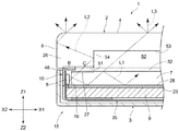
図1は、本発明に係る照明モジュール1を示す外観図であり、上段に記載の(A)は斜視図、下段に記載の(B)は側面図である。なお、以下の説明において、矢視X1方向を右側(右辺側)、矢視X2方向を左側(左辺側)、矢視Y1方向を前方(前辺側)、矢視Y2方向を後方(後辺側)、矢視Z1方向を上方向(上面側)、矢視Z2方向を下方向(下面側)とそれぞれ規定して説明する。また、矢視Z1方向を表面側、矢視Z2方向を裏面側と記載することがある。   FIG. 1 is an external view showing an illumination module 1 according to the present invention, wherein (A) in the upper part is a perspective view and (B) in the lower part is a side view. In the following description, the arrow X1 direction is the right side (right side), the arrow X2 direction is the left side (left side), the arrow Y1 direction is the front (front side), and the arrow Y2 direction is the rear (rear side). Side), the arrow Z1 direction is defined as an upward direction (upper surface side), and the arrow Z2 direction is defined as a downward direction (lower surface side). Moreover, the arrow Z1 direction may be described as the front surface side, and the arrow Z2 direction may be described as the back surface side.

図1(A),(B)に示すように、照明モジュール1は、表面側に拡散板2が配置され、裏面側にケース部材である保持ケース3が配置されている。保持ケース3は、熱伝導率が高い金属板で形成されるが、軽量化の観点からアルミニウム製とすることが好ましい。
拡散板2と保持ケース3は、複数の固定部材によって一体化されている。拡散板2の上面は、外部に光を射出する第2光出射面4である。なお、固定部材による固定構造については、図6〜図9を参照して後述する。保持ケース3の外周側面5は、拡散板2の外周側面6と同一面内に配置されるか、拡散板2の外周側面6の内側に配置される。拡散板2と保持ケース3で挟まれた空間には、後述する導光板7、光源であるLED光源8、フレーム9、および光遮蔽フレーム10などが収容されている(図2、図4参照)。保持ケース3の4辺の周縁部11の厚みは、周縁部11の内側部分12の厚みよりも薄く形成されている。すなわち、内側部分12は、周縁部11に対して凸となっている。また、内側部分12は、周縁部11から少しくぼんだ溝部24から突出するように形成されている(図3参照)。なお、以下に示す照明モジュール1は、左右方向の長さが600mm、前後方向の長さ(幅)が300mmの長方形で、周縁部11の厚みが約10mm、内側部分の厚みが約12mmの薄い扁平な場合を例示している。
As shown to FIG. 1 (A), (B), as for the illumination module 1, the diffusion plate 2 is arrange | positioned at the surface side, and the holding case 3 which is a case member is arrange | positioned at the back surface side. The holding case 3 is formed of a metal plate having a high thermal conductivity, but is preferably made of aluminum from the viewpoint of weight reduction.
The diffusion plate 2 and the holding case 3 are integrated by a plurality of fixing members. The upper surface of the diffusion plate 2 is a second light emitting surface 4 that emits light to the outside. The fixing structure using the fixing member will be described later with reference to FIGS. The outer peripheral side surface 5 of the holding case 3 is disposed in the same plane as the outer peripheral side surface 6 of the diffusion plate 2 or is disposed inside the outer peripheral side surface 6 of the diffusion plate 2. The space sandwiched between the diffusion plate 2 and the holding case 3 accommodates a light guide plate 7 described later, an LED light source 8 as a light source, a frame 9, a light shielding frame 10, and the like (see FIGS. 2 and 4). . The thickness of the peripheral edge 11 on the four sides of the holding case 3 is formed thinner than the thickness of the inner portion 12 of the peripheral edge 11. That is, the inner portion 12 is convex with respect to the peripheral edge portion 11. Moreover, the inner part 12 is formed so that it may protrude from the groove part 24 slightly depressed from the peripheral part 11 (refer FIG. 3). The lighting module 1 shown below has a rectangular shape with a length of 600 mm in the left-right direction and a length (width) of 300 mm in the front-rear direction, a thickness of the peripheral portion 11 of about 10 mm, and a thickness of the inner portion of about 12 mm. A flat case is illustrated.

図2は、照明モジュール1を表面側から見た平面図で、各光源部の概略の配置を示す説明図である。図2に示すように、照明モジュール1は、左辺側の第1の光源部15と右辺側の第2の光源部16と、前辺側の第3の光源部17と、後辺側の第4の光源部18を有している。第1の光源部15と第2の光源部16、第3の光源部17と第4の光源部18は、互いに対向するように配置されている。第1の光源部15から第4の光源部18の4つの光源部のそれぞれには、複数のLED光源8が導光板7の各辺に設けられた端面19に沿って配列されている。また、LED光源8および端面19を覆うように光遮蔽フレーム10が配置されている。第1の光源部15から第4の光源部の4つの光源部の各々に配置されるLED光源8の数やピッチは、図2では分かりやすく図示するために簡略化して表しているが、要求される明るさや第2光出射面4の広さによって適宜選択可能である。なお、図2に示すように、光遮蔽フレーム10は、左辺側と右辺側は同じもので対向する関係にあり、前辺側と後辺側は同じもので対向する関係にあり、左右のものと前後のものは、長さのみが異なるものとなっているため、以下の説明では、左辺側を例示して説明する。   FIG. 2 is a plan view of the illumination module 1 as viewed from the front side, and is an explanatory diagram showing a schematic arrangement of each light source unit. As shown in FIG. 2, the illumination module 1 includes a first light source unit 15 on the left side, a second light source unit 16 on the right side, a third light source unit 17 on the front side, and a second light source unit 17 on the rear side. 4 light source portions 18 are provided. The 1st light source part 15 and the 2nd light source part 16, and the 3rd light source part 17 and the 4th light source part 18 are arrange | positioned so that it may mutually oppose. In each of the four light source units from the first light source unit 15 to the fourth light source unit 18, a plurality of LED light sources 8 are arranged along end surfaces 19 provided on each side of the light guide plate 7. In addition, the light shielding frame 10 is disposed so as to cover the LED light source 8 and the end surface 19. The number and pitch of the LED light sources 8 arranged in each of the four light source units from the first light source unit 15 to the fourth light source unit are simplified for easy understanding in FIG. The brightness can be selected as appropriate depending on the brightness of the light and the width of the second light exit surface 4. In addition, as shown in FIG. 2, the light shielding frame 10 has a left side and a right side that are the same and face each other, and the front side and the rear side are the same and face each other. Since the front and rear are different only in length, in the following description, the left side will be described as an example.

図2に示すように、導光板7には、各4辺の端面19からLED光源8に向かう方向に突出される凸部20が間隔を開けて設けられ、隣り合う凸部20の間にLED光源8が配設されている(図4、図6も参照)。図2に示す凸部20の位置と、隣り合う凸部20の間に配置されるLED光源8の数や位置は、分かりやすくするために簡略化して表しているが、任意に設定可能である。   As shown in FIG. 2, the light guide plate 7 is provided with convex portions 20 that protrude in the direction from the end surfaces 19 of the four sides toward the LED light source 8 at intervals, and the LED 20 is disposed between the adjacent convex portions 20. A light source 8 is provided (see also FIGS. 4 and 6). The number and position of the LED light sources 8 arranged between the convex portions 20 shown in FIG. 2 and the adjacent convex portions 20 are simplified for easy understanding, but can be arbitrarily set. .

図3は、照明モジュール1を裏面側から見た斜視図である。保持ケース3には、4つの辺に連続する周縁部11と、周縁部11の内側において周縁部11よりも凸となる内側部分12と、周縁部11と内側部分12の間に内側部分12を囲む溝部24が設けられている。周縁部11には、固定部材として第1のネジであるネジ21、第2のネジであるネジ22が配置されている。また、溝部24には、固定部材として第3のネジであるネジ23が配置されている。ネジ21による固定構造は図6を参照し、ネジ22による固定構造は図7を参照し、ネジ23による固定構造は図8および図9を参照して後述する。なお、対向する左辺側と右辺側の各ネジの配置は対となるように配置され、前辺側と後辺側の各ネジの配置も対となるように配置されている。ネジ21、ネジ22およびネジ23各々の数と配置距離(ピッチ)は、照明モジュール1の平面サイズによって適宜設定される。   FIG. 3 is a perspective view of the illumination module 1 as seen from the back side. The holding case 3 includes a peripheral edge portion 11 that is continuous with the four sides, an inner portion 12 that is more convex than the peripheral edge portion 11 inside the peripheral edge portion 11, and an inner portion 12 between the peripheral edge portion 11 and the inner portion 12. An enclosing groove 24 is provided. A screw 21 that is a first screw and a screw 22 that is a second screw are disposed on the peripheral edge 11 as fixing members. Further, a screw 23 as a third screw is disposed in the groove portion 24 as a fixing member. The fixing structure with the screw 21 will be described later with reference to FIG. 6, the fixing structure with the screw 22 will be described with reference to FIG. 7, and the fixing structure with the screw 23 will be described later with reference to FIGS. In addition, the arrangement | positioning of each screw | thread on the left side and right side which oppose is arrange | positioned so that it may become a pair, and the arrangement | positioning of each screw | thread of the front side and back side is also arranged so that it may become a pair. The number and the arrangement distance (pitch) of each of the screw 21, screw 22, and screw 23 are appropriately set according to the planar size of the lighting module 1.

図4は、図3の切断線A−Aで切断した切断面を示す断面図である。前述したように、照明モジュール1は、左辺側の第1の光源部15と右辺側の第2の光源部16と、前辺側の第3の光源部17と後辺側の第4の光源部18を備えている。第1の光源部15から第4の光源部18の各光源部のそれぞれは、構成要素の数やサイズが異なるものの、構成要素の一つひとつは同様に説明可能であるため、以下の説明では、左辺側の第1の光源部15を代表例として説明する。   4 is a cross-sectional view showing a cut surface taken along the cutting line AA of FIG. As described above, the illumination module 1 includes the first light source 15 on the left side, the second light source 16 on the right side, the third light source 17 on the front side, and the fourth light source on the rear side. A portion 18 is provided. Although each of the light source units of the first light source unit 15 to the fourth light source unit 18 is different in the number and size of the constituent elements, each of the constituent elements can be described in the same manner. The first light source unit 15 on the side will be described as a representative example.

図4に示すように、照明モジュール1は、導光板7と、導光板7の左辺側の端面19に沿って配列された複数のLED光源8と、LED光源8が出射した光が直接拡散板2に入射されないように、また、外部に漏れないように遮蔽する断面U字形状の光遮蔽フレーム10と、導光板7の表面側に沿うように配置される拡散板2などを備えている。なお、第1光源部15とは、照明モジュール1の左辺側において、端面19と、複数のLED光源8と、光遮蔽フレーム10と、拡散板2の左辺側に形成された凸条部26と、凸条部26に対向する部分である導光板7の周縁部27などが配置された部分を言う。なお、端面19は、図2に示したように、隣り合う凸部20の間に形成される導光板7の側面(凸部20に対する底面に相当する)である。   As shown in FIG. 4, the illumination module 1 includes a light guide plate 7, a plurality of LED light sources 8 arranged along an end surface 19 on the left side of the light guide plate 7, and light emitted from the LED light source 8 is directly diffused. The light shielding frame 10 having a U-shaped cross section that shields the light from entering the light source 2 so as not to leak to the outside, and the diffusion plate 2 disposed along the surface side of the light guide plate 7 are provided. In addition, the 1st light source part 15 is the end surface 19, the some LED light source 8, the light shielding frame 10, and the protruding item | line part 26 formed in the left side of the diffusion plate 2 in the left side of the illumination module 1. The part where the peripheral part 27 of the light-guide plate 7 etc. which are the parts facing the protruding item | line part 26 are arrange | positioned. As shown in FIG. 2, the end surface 19 is a side surface of the light guide plate 7 formed between adjacent convex portions 20 (corresponding to a bottom surface with respect to the convex portion 20).

なお、図4では、光源としてLED光源8を用いた場合を例示しているが、光源としては、CCFL(Cold Cathode Fluorescent Lamp:冷陰極蛍光管)、電球(たとえば白熱電球)や蛍光灯などを用いることが可能であって、光源の種類は限定されない。しかし、LED光源は、他の光源と比べ、消費電力が小さい、発熱量が小さい、小型化しやすい、並びにコストなどで優れている。したがって、以下の各図の説明では、光源としてLED光源8を用いた場合を説明する。   4 illustrates the case where the LED light source 8 is used as the light source, the CCFL (Cold Cathode Fluorescent Lamp), a light bulb (for example, an incandescent light bulb), a fluorescent light, etc. The type of the light source is not limited. However, LED light sources are superior to other light sources in terms of low power consumption, low calorific value, easy miniaturization, and cost. Therefore, in the following description of each figure, the case where the LED light source 8 is used as the light source will be described.

導光板7の裏面28側(拡散板2に対して反対側の面)には、反射板29が配置されている。反射板29は、薄い反射シートでもよく、導光板7の裏面28に貼着してもよい。また、反射板に替えて導光板7の裏面28に反射コートを設けてもよく、また、省略することも可能である。反射板29の平面形状は、導光板7の平面外形形状とほぼ同じであるが、LED光源8の下方の少なくとも一部を覆うように配置される。反射板29は、導光板7の裏面28に密接され、導光板7内を進行する光を拡散板2の方向に反射させる機能を有する。反射板29の下方側には、フレーム9が配設されている。   On the back surface 28 side of the light guide plate 7 (surface opposite to the diffusion plate 2), a reflection plate 29 is disposed. The reflection plate 29 may be a thin reflection sheet or may be attached to the back surface 28 of the light guide plate 7. In addition, a reflective coat may be provided on the back surface 28 of the light guide plate 7 instead of the reflective plate, or may be omitted. The planar shape of the reflecting plate 29 is substantially the same as the planar outer shape of the light guide plate 7, but is disposed so as to cover at least a part below the LED light source 8. The reflection plate 29 is in close contact with the back surface 28 of the light guide plate 7 and has a function of reflecting light traveling in the light guide plate 7 in the direction of the diffusion plate 2. A frame 9 is disposed below the reflecting plate 29.

フレーム9は、熱伝導率が高い金属製の板材で形成されるが、軽量化の観点からアルミニウム製とすることが好ましい。フレーム9は、図2に示すように、平面形状が長方形の枠形状をしており、外周枠部30の内側は表裏を貫通する開口部31となっている。外周枠部30の4辺は、ほぼ同じ幅である。したがって、開口部31の平面形状は長方形である。フレーム9は、後述するLED基板35および光遮蔽フレーム10を一体化する機能を有する(図6参照)。なお、図示は省略するが、フレーム9は、開口部31の対角を連結する梁を形成し、補強するようにしてもよい。   The frame 9 is formed of a metal plate material having a high thermal conductivity, but is preferably made of aluminum from the viewpoint of weight reduction. As shown in FIG. 2, the frame 9 has a rectangular frame shape, and the inside of the outer peripheral frame portion 30 is an opening portion 31 penetrating the front and back. The four sides of the outer peripheral frame portion 30 have substantially the same width. Therefore, the planar shape of the opening 31 is a rectangle. The frame 9 has a function of integrating an LED substrate 35 and a light shielding frame 10 described later (see FIG. 6). In addition, although illustration is abbreviate | omitted, the flame | frame 9 may form the beam which connects the diagonal of the opening part 31, and you may make it reinforce it.

導光板7は、光透過率が高いアクリル系樹脂で成形され、LED光源8から出射される光が入射される端面19と、拡散板2と対向する第1光出射面32、および第1光出射面32の反対側の面となる裏面28を備えている。端面19は、LED光源8から出射される光の入射面であり、第1光出射面32は、導光板7から拡散板2に対して光を出射する光出射面である。なお、前述した凸部20のLED光源8に対向する側面も端面19と同様に、LED光源8から出射される光が入射される光入射面といえる。裏面28は、反射板29に密接されると共に、導光板7の内部を進行する光の反射面として機能する。LED光源8は、光源基板であるLED基板35に実装され、端面19に沿って配置されている。LED光源8は、導光板7の厚み範囲に配置されるが、導光板7の厚み方向のほぼ中央に配置すればなおよい。中央に配置することで、中央に配置しない場合に比べて第1光出射面32から出射する光量が多くなる。   The light guide plate 7 is formed of an acrylic resin having a high light transmittance, and an end surface 19 on which light emitted from the LED light source 8 is incident, a first light emitting surface 32 facing the diffusion plate 2, and first light. A back surface 28 which is a surface opposite to the emission surface 32 is provided. The end surface 19 is an incident surface for light emitted from the LED light source 8, and the first light emitting surface 32 is a light emitting surface that emits light from the light guide plate 7 to the diffusion plate 2. Note that the side surface of the convex portion 20 facing the LED light source 8 can also be said to be a light incident surface on which light emitted from the LED light source 8 is incident, like the end surface 19. The back surface 28 is in close contact with the reflection plate 29 and functions as a reflection surface for light traveling inside the light guide plate 7. The LED light source 8 is mounted on an LED substrate 35 that is a light source substrate, and is disposed along the end surface 19. Although the LED light source 8 is disposed within the thickness range of the light guide plate 7, it is more preferable that the LED light source 8 is disposed at substantially the center in the thickness direction of the light guide plate 7. By disposing at the center, the amount of light emitted from the first light exit surface 32 becomes larger than when not disposed at the center.

なお、LED光源8から導光板7の端面19に入射される光の強さは、LED光源8と端面19の距離に左右される。すなわち、LED光源8が端面19に近づけば入射される光の強さが増し、遠ざかれば入射される光の強さが減る。図2に示したように、導光板7には、各4辺の端面19からLED光源8の方向(LED基板35側に)に向かって凸部20が設けられ、隣り合う凸部20の間にLED光源8を配設するようにしている。図4に示すように、凸部20の先端面は、LED基板35の基板側部36に当接されている。つまり、LED光源8と端面19との間隔は、凸部20の先端面の端面19からの距離で規制される。一方、LED基板35のLED光源8が実装される基板側部36は、光遮蔽フレーム10の側部45で左方への移動が規制される。このようにして、LED光源8と端面19の距離がほぼ一定に保持されることで、端面19に入射される光の強さは、ほぼ一定となるように管理可能となる。   The intensity of light incident on the end surface 19 of the light guide plate 7 from the LED light source 8 depends on the distance between the LED light source 8 and the end surface 19. That is, the intensity of the incident light increases as the LED light source 8 approaches the end face 19, and the intensity of the incident light decreases as it moves away. As shown in FIG. 2, the light guide plate 7 is provided with convex portions 20 from the end surfaces 19 of the four sides toward the LED light source 8 (to the LED substrate 35 side), and between the adjacent convex portions 20. The LED light source 8 is arranged on the front. As shown in FIG. 4, the tip surface of the convex portion 20 is in contact with the substrate side portion 36 of the LED substrate 35. That is, the distance between the LED light source 8 and the end surface 19 is regulated by the distance from the end surface 19 of the tip surface of the convex portion 20. On the other hand, the board side part 36 on which the LED light source 8 of the LED board 35 is mounted is restricted from moving leftward by the side part 45 of the light shielding frame 10. In this way, the distance between the LED light source 8 and the end face 19 is kept substantially constant, so that the intensity of light incident on the end face 19 can be managed to be substantially constant.

LED基板35は、フレキシブル基板であって、図10に示すように、LED光源8が実装される基板側部36と、基板側部36の下方側において基板側部36に直交するように曲げられて延在される回路接続部37を有する。回路接続部37は、右辺方向に向かって延長され、接続基板38を介して回路部39に接続される(図10参照)。回路部39は、LED光源8の点灯制御を行うICチップや抵抗素子などの回路素子を有している。LED基板35は、回路接続部37を光遮蔽フレーム10に設けられた孔部40に挿通することで、回路接続部37を保持ケース3と光遮蔽フレーム10の下板部41の間に配置できるようになっている。   The LED substrate 35 is a flexible substrate, and is bent so as to be orthogonal to the substrate side portion 36 on the lower side of the substrate side portion 36 and the substrate side portion 36 on which the LED light source 8 is mounted, as shown in FIG. The circuit connection part 37 is extended. The circuit connection portion 37 extends toward the right side and is connected to the circuit portion 39 via the connection substrate 38 (see FIG. 10). The circuit unit 39 includes circuit elements such as an IC chip and a resistance element that perform lighting control of the LED light source 8. The LED board 35 can be disposed between the holding case 3 and the lower plate portion 41 of the light shielding frame 10 by inserting the circuit connecting portion 37 into the hole 40 provided in the light shielding frame 10. It is like that.

LED光源8を構成するLED素子の一つ一つは、白色LED素子であって、回路部39からの入力信号によって、各LED素子からの発光を制御する。なお、LED素子として、赤色LED素子、緑色LED素子および青色LED素子がひとつにパッケージされたタイプのLEDランプを用いることも可能で、回路部39からの入力信号によって、各色のLED素子からの発光、混色により指定色の発光を行うことができる。なお、LED光源8は、LED基板35に実装されて、フレーム9の外周枠部30にネジ21によって固定される。この固定構造は図6を、LED基板35と回路部39の接続構造は図10を参照して後述する。   Each of the LED elements constituting the LED light source 8 is a white LED element, and the light emission from each LED element is controlled by an input signal from the circuit unit 39. In addition, it is also possible to use an LED lamp of a type in which a red LED element, a green LED element, and a blue LED element are packaged together as the LED element, and light emission from the LED elements of each color according to an input signal from the circuit unit 39. The designated color can be emitted by mixing the colors. The LED light source 8 is mounted on the LED substrate 35 and fixed to the outer peripheral frame portion 30 of the frame 9 with screws 21. The fixing structure will be described later with reference to FIG. 6, and the connection structure between the LED substrate 35 and the circuit unit 39 will be described later with reference to FIG.

光遮蔽フレーム10は、アルミニウム製の板を曲げ折りして成形されている。光遮蔽フレーム10は、端面19に沿いつつ、LED基板35の基板側部36の背面側に配置される側部45と、側部45の拡散板2側端部から側部45に直交し右辺側に延長される上板部46と、保持ケース3側端部から側部45に直交し、右辺側に延長される下板部41を有する。上板部46は、第1光出射面32側に延長されている。上板部46は光遮蔽部であって、以下の説明では光遮蔽部46と記載する。光遮蔽フレーム10は、側部45と下板部41の接続部にかけて表裏を貫通する孔部40を有する。孔部40には、LED基板35の回路接続部37が挿通される。光遮蔽フレーム10は、光遮蔽部46と下板部41の間に導光板7と反射板29およびフレーム9を配設し、ネジ21で一体化して光源ユニット50を構成する(図6参照)。光遮蔽部46は、LED光源8から出射される光がそのまま拡散板2に入射しないように、つまり、LED光源8の光が、LED光源8よりも図示上方向に配置される拡散板2に直接入射させない光遮蔽機能を有する。   The light shielding frame 10 is formed by bending and folding an aluminum plate. The light shielding frame 10 extends along the end surface 19, the side portion 45 disposed on the back side of the substrate side portion 36 of the LED substrate 35, and the right side orthogonal to the side portion 45 from the diffusion plate 2 side end portion of the side portion 45. An upper plate portion 46 that extends to the side, and a lower plate portion 41 that is orthogonal to the side portion 45 from the end portion on the holding case 3 side and extends to the right side. The upper plate portion 46 extends to the first light exit surface 32 side. The upper plate portion 46 is a light shielding portion, and will be referred to as a light shielding portion 46 in the following description. The light shielding frame 10 has a hole 40 that penetrates the front and back from the connecting portion between the side portion 45 and the lower plate portion 41. The circuit connection part 37 of the LED substrate 35 is inserted through the hole 40. In the light shielding frame 10, the light guide plate 7, the reflection plate 29, and the frame 9 are disposed between the light shielding portion 46 and the lower plate portion 41, and are integrated by screws 21 to constitute the light source unit 50 (see FIG. 6). . The light shielding unit 46 prevents the light emitted from the LED light source 8 from entering the diffusion plate 2 as it is, that is, the light from the LED light source 8 is directed to the diffusion plate 2 arranged in the upward direction of the LED light source 8. It has a light shielding function that prevents direct incidence.

拡散板2は、光散乱粒子が含まれたアクリル系樹脂で成形されており、図2に示すように平面視において長方形であって、照明モジュール1の平面形状および平面サイズを規定している。つまり、照明モジュール1を真上から見たとき、拡散板2の下方にある保持ケース3は見えないようになっている。拡散板2には、導光板7の第1光出射面32に向かって突設された凸条部26が形成されている。凸条部26は、左辺側の第1光源部15、右辺側の第2光源部16、前辺側の第3光源部17、および後辺側の第4光源部18に連続するように形成されている。凸条部26は、導光板7の周縁部27に対向する位置に配置されている。凸条部26の導光板7に対向する先端部平面は、導光板7の第1光出射面32から出射された光が入射される第2光入射面51である。つまり、導光板7の周縁部27は、凸条部26の第2光入射面51と対向する部分をいう。   The diffuser plate 2 is formed of an acrylic resin containing light scattering particles, and is rectangular in a plan view as shown in FIG. 2, and defines the planar shape and planar size of the illumination module 1. That is, when the illumination module 1 is viewed from directly above, the holding case 3 below the diffusion plate 2 is not visible. On the diffusing plate 2, a ridge 26 is formed so as to project toward the first light exit surface 32 of the light guide plate 7. The ridge 26 is formed to be continuous with the first light source 15 on the left side, the second light source 16 on the right side, the third light source 17 on the front side, and the fourth light source 18 on the rear side. Has been. The protruding portion 26 is disposed at a position facing the peripheral portion 27 of the light guide plate 7. The tip plane of the ridge 26 facing the light guide plate 7 is a second light incident surface 51 on which light emitted from the first light exit surface 32 of the light guide plate 7 is incident. That is, the peripheral edge portion 27 of the light guide plate 7 refers to a portion facing the second light incident surface 51 of the ridge portion 26.

拡散板2には、LED光源8の配列方向に直交する平面における断面形状において、凸条部26に囲まれた凹部空間52が形成されている。凹部空間52の底面(第1光射出面32に対向する面)である第1光入射面53は、第1光出射面32から出射した光が入射する光入射面である。拡散板2の外周側面6は、空気に接する面であり、凸条部26の内側側面54は凹部空間52に面し、空気に接する面である。したがって、凸条部26の内側から外周側面6に臨界角を超えて入射する光は、外周側面6で全反射する。また、凸条部26の内側から内側側面54に臨界角を超えて入射する光は、内側側面54で全反射する。外周側面6と内側側面54とは互いに平行な面であり、第2光入射面51は、外周側面6および内側側面54に直交する面である。   In the diffusing plate 2, a recessed space 52 surrounded by the protruding strips 26 is formed in a cross-sectional shape in a plane orthogonal to the arrangement direction of the LED light sources 8. The first light incident surface 53, which is the bottom surface of the recessed space 52 (the surface facing the first light emitting surface 32), is a light incident surface on which light emitted from the first light emitting surface 32 is incident. The outer peripheral side surface 6 of the diffusing plate 2 is a surface in contact with air, and the inner side surface 54 of the ridge 26 is a surface in contact with the recess space 52 and in contact with air. Therefore, light that enters the outer peripheral side surface 6 beyond the critical angle from the inside of the ridge 26 is totally reflected by the outer peripheral side surface 6. Further, light that enters the inner side surface 54 from the inside of the ridge 26 beyond the critical angle is totally reflected by the inner side surface 54. The outer peripheral side surface 6 and the inner side surface 54 are surfaces parallel to each other, and the second light incident surface 51 is a surface orthogonal to the outer peripheral side surface 6 and the inner side surface 54.

凸条部26の第2光入射面51は、LED光源8あるいは第1光出射面32(特に周縁部27)から出射する光が光遮蔽部46により遮蔽される領域である遮蔽領域Bと、光遮蔽部46により遮蔽されることなく光が入射する領域である入射領域Cとを有する。すなわち、凸条部26の第2光入射面51と、導光板7の周縁部27との間に光遮蔽部46を配置することにより、周縁部26から出射した光が第2光入射面51に入射する光量を制限することができる。遮蔽領域Bは、LED光源8から出射された光が導光板7を介さずに直接拡散板2に入射しない広さ(左右方向の幅寸法)を少なくとも有する。また、遮蔽領域Bの広さ(左右方向の幅寸法)と入射領域Cの広さ(左右方向の幅寸法)は、第1光出射面32から第2光入射面51に入射する光が第2光出射面4から出射する際に、第2光出射面4の全体の明るさが均一となるように設定される。第1光出射面32から第2光入射面51に入射した光は主に、第2光出射面4の周縁部から出射することになる。第2光出射面4の周縁部の明るさが、この周縁部よりも内側の明るさに近づくように、遮蔽領域Bの広さおよび入射領域Cの広さが設定される。遮蔽領域Bの広さをX、入射領域Cの広さをYとすると、X:Yは1:0.5〜1:5が好ましく、X:Yは1:1〜1:3がより好ましい。拡散板2は、凸条部26の第2光入射面51で光遮蔽フレーム10の光遮蔽部46と密接される。右辺側の光遮蔽フレーム10、前辺側の光遮蔽フレーム10および後辺側の光遮蔽フレーム10も、左辺側の光遮蔽フレーム10と同様な条件で設定される。   The second light incident surface 51 of the ridge portion 26 includes a shielding region B that is a region where light emitted from the LED light source 8 or the first light emitting surface 32 (particularly the peripheral portion 27) is shielded by the light shielding portion 46; And an incident region C that is a region where light is incident without being shielded by the light shielding unit 46. That is, by arranging the light shielding portion 46 between the second light incident surface 51 of the ridge portion 26 and the peripheral portion 27 of the light guide plate 7, the light emitted from the peripheral portion 26 is reflected by the second light incident surface 51. The amount of light incident on can be limited. The shielding region B has at least a width (width dimension in the left-right direction) where the light emitted from the LED light source 8 does not directly enter the diffusion plate 2 without passing through the light guide plate 7. In addition, the width of the shielding area B (width dimension in the left-right direction) and the width of the incident area C (width dimension in the left-right direction) are such that light incident on the second light incident surface 51 from the first light exit surface 32 is the first. When the light exits from the two light exit surfaces 4, the overall brightness of the second light exit surface 4 is set to be uniform. The light that has entered the second light incident surface 51 from the first light emitting surface 32 is emitted mainly from the peripheral edge of the second light emitting surface 4. The width of the shielding area B and the width of the incident area C are set so that the brightness of the peripheral edge of the second light exit surface 4 approaches the brightness inside the peripheral edge. When the area of the shielding area B is X and the area of the incident area C is Y, X: Y is preferably 1: 0.5 to 1: 5, and X: Y is more preferably 1: 1 to 1: 3. . The diffusing plate 2 is in close contact with the light shielding portion 46 of the light shielding frame 10 at the second light incident surface 51 of the ridge portion 26. The light shielding frame 10 on the right side, the light shielding frame 10 on the front side, and the light shielding frame 10 on the rear side are also set under the same conditions as the light shielding frame 10 on the left side.

続いて、LED光源8から出射された光が、第2光出射面4から出射するまでの光の経路について、図5を参照しながら説明する。   Subsequently, a path of light until the light emitted from the LED light source 8 is emitted from the second light emission surface 4 will be described with reference to FIG.

図5は、LED光源8から出射した光が拡散板2の第2光出射面4から出射するまでの光の経路を示す説明図である。左辺側の第1の光源部15側のLED光源8から出射された光の一部は、導光板7の端面19から導光板7内に進入し、たとえば、破線L1で示すように、導光板7の第1光出射面32および裏面28で全反射されながら右辺側に向かって進み、いずれは、第1光出射面32から出射される。LED光源8から出射された光の他の一部には、第1光出射面32または裏面28で全反射されることなく、第1光出射面32から出射されるものもある。   FIG. 5 is an explanatory diagram showing a light path until the light emitted from the LED light source 8 is emitted from the second light emitting surface 4 of the diffusion plate 2. A part of the light emitted from the LED light source 8 on the first light source unit 15 side on the left side enters the light guide plate 7 from the end surface 19 of the light guide plate 7 and, for example, as indicated by a broken line L1, 7 proceeds toward the right side while being totally reflected by the first light emitting surface 32 and the back surface 28, and both are emitted from the first light emitting surface 32. Other part of the light emitted from the LED light source 8 may be emitted from the first light emitting surface 32 without being totally reflected by the first light emitting surface 32 or the back surface 28.

右辺側の第2の光源部16のLED光源8から出射された光も左辺側と同様に導光板7の右辺側の端面19から導光板7内に進入する。導光板7内に入射された光は、左辺側に進み、導光板7の第1光出射面32および裏面28で全反射され、いずれは、第1光出射面32から出射される。   The light emitted from the LED light source 8 of the second light source unit 16 on the right side also enters the light guide plate 7 from the end surface 19 on the right side of the light guide plate 7 in the same manner as the left side. The light that has entered the light guide plate 7 travels to the left side and is totally reflected by the first light exit surface 32 and the back surface 28 of the light guide plate 7, and either is emitted from the first light exit surface 32.

同様に、前辺側の第3の光源部17のLED光源8から出射された光も、右辺側および左辺側と同様に導光板7の前辺側の端面19から導光板7内に進入する。導光板7内に入射された光は、後辺側に進み、導光板7の第1光出射面32および裏面28で全反射され、いずれは、第1光出射面32から出射される。後辺側の第4の光源部18のLED光源8から出射された光も、前辺側と同様に導光板7の後辺側の端面19から導光板7内に進入する。導光板7内に入射された光は、前辺側に進み、導光板7の第1光出射面32および裏面28で全反射され、いずれは、第1光出射面32から出射される。   Similarly, the light emitted from the LED light source 8 of the third light source unit 17 on the front side also enters the light guide plate 7 from the end surface 19 on the front side of the light guide plate 7 in the same manner as the right side and the left side. . The light that has entered the light guide plate 7 travels to the rear side, and is totally reflected by the first light output surface 32 and the back surface 28 of the light guide plate 7, and either is output from the first light output surface 32. The light emitted from the LED light source 8 of the fourth light source unit 18 on the rear side also enters the light guide plate 7 from the end surface 19 on the rear side of the light guide plate 7 in the same manner as the front side. The light that has entered the light guide plate 7 travels to the front side and is totally reflected by the first light exit surface 32 and the back surface 28 of the light guide plate 7, and either is emitted from the first light exit surface 32.

導光板7の第1光出射面32から出射された光は、拡散板2の凹部空間52の底面である第1光入射面53、および凸条部26の第2光入射面51に入射され、拡散板2内を進行して第2光出射面4から出射される。拡散板2には光散乱粒子が含有されている。そのため、拡散板2内に入射した光が拡散板2内で散乱されることで、第2光出射面4から出射する光の照度分布の均一化を図ることができる。   The light emitted from the first light emitting surface 32 of the light guide plate 7 is incident on the first light incident surface 53 which is the bottom surface of the concave space 52 of the diffusion plate 2 and the second light incident surface 51 of the ridge 26. Then, the light travels through the diffusion plate 2 and is emitted from the second light exit surface 4. The diffusion plate 2 contains light scattering particles. Therefore, the light incident on the diffusion plate 2 is scattered in the diffusion plate 2, so that the illuminance distribution of the light emitted from the second light emission surface 4 can be made uniform.

LED光源8から出射される光は、LED光源8に近い位置では明るく、遠くなるに従い暗くなる。しかしながら、照明モジュール1は、左辺側の第1の光源部15と右辺側の第2の光源部16、および前辺側の第3の光源部17と後辺側の第4の光源部18を備えており、相互に右辺側、左辺側、および後辺側、前辺側に向かって光が進行するので、光が互いに補完しあい、導光板7の第1光射出面32の明るさが均斉化される。   The light emitted from the LED light source 8 is bright at a position close to the LED light source 8 and becomes darker as the distance increases. However, the illumination module 1 includes a first light source unit 15 on the left side, a second light source unit 16 on the right side, a third light source unit 17 on the front side, and a fourth light source unit 18 on the rear side. Since the light travels toward the right side, the left side, the rear side, and the front side, the light complements each other and the brightness of the first light exit surface 32 of the light guide plate 7 is uniform. It becomes.

図5に示すように、導光板7のLED光源8に近い周縁部27には、光遮蔽フレーム10の光遮蔽部46が配置されている。光遮蔽部46により、LED光源8および周縁部27から凸条部26へ入射する光が制限される。つまり、第2光入射面51の一部は遮蔽領域Bとなっていて、LED光源8から出射されて第2光入射面51に向かう光の一部は遮蔽領域Bで、すなわち光遮蔽部46により遮蔽される。一方、入射領域Cでは、第1光出射面32から凸条部26の第2光入射面51に向けて出射された光の一部が入射される。   As shown in FIG. 5, the light shielding portion 46 of the light shielding frame 10 is disposed on the peripheral edge portion 27 of the light guide plate 7 near the LED light source 8. The light shielding part 46 restricts the light incident on the ridge part 26 from the LED light source 8 and the peripheral part 27. That is, a part of the second light incident surface 51 is the shielding region B, and a part of the light emitted from the LED light source 8 and directed to the second light incident surface 51 is the shielding region B, that is, the light shielding part 46. It is shielded by. On the other hand, in the incident region C, a part of the light emitted from the first light emitting surface 32 toward the second light incident surface 51 of the ridge 26 is incident.

凸条部26の第2光入射面51から入射された光の一部は、破線L2で示すように、凸条部26の内側側面54と外周側面6の間で全反射されながら、また、光散乱粒子で散乱されながら進む。そして、拡散板2の第2光出射面4の主として凸条部26の配置領域上方、すなわち、第2光出射面4のLED光源8が配置される側の周縁部から出射される。凸条26内に入射された光の一部は、内側側面54と外周側面6とで全反射しながら、また、光散乱粒子で散乱されながら進むことで、第2光出射面4から拡散状態で出射される。凸条部26に入射した光は主として凸条部26の配置位置の上方から出射する。このようにして、周縁部を含めて第2光出射面4の明るさが均斉化される。なお、第2光出射面4から出射する光は、光散乱粒子で拡散されるので、出射された光の強さと色調(光の波長)は、第2光出射面53の上方において、どの方向から見ても変わらないようになっている。   A part of the light incident from the second light incident surface 51 of the ridge portion 26 is totally reflected between the inner side surface 54 and the outer peripheral side surface 6 of the ridge portion 26 as indicated by a broken line L2, and Proceed while being scattered by light scattering particles. And it is radiate | emitted mainly from the arrangement | positioning area | region of the protruding item | line part 26 of the 2nd light-projection surface 4 of the diffusion plate 2, ie, the peripheral part by the side of the LED light source 8 side of the 2nd light-projection surface 4. A part of the light incident on the ridge 26 is reflected from the inner side surface 54 and the outer peripheral side surface 6 and travels while being scattered by the light scattering particles, thereby diffusing from the second light emitting surface 4. It is emitted at. The light incident on the ridges 26 is emitted mainly from above the arrangement position of the ridges 26. In this way, the brightness of the second light exit surface 4 including the peripheral portion is equalized. In addition, since the light emitted from the second light emitting surface 4 is diffused by the light scattering particles, the intensity and color tone (wavelength of light) of the emitted light can be determined in any direction above the second light emitting surface 53. Even if it sees from, it has become the same.

続いて、照明モジュール1の各部の固定構造について図6〜図9を参照して説明する。これら固定構造は、第1の光源部15から第4の光源部18の各光源部共に、同様な構造であるため、以下の説明では、左辺側の第1の光源部15を例示して説明する。   Subsequently, a fixing structure of each part of the illumination module 1 will be described with reference to FIGS. Since these fixing structures are the same structure for each of the light source units from the first light source unit 15 to the fourth light source unit 18, in the following description, the first light source unit 15 on the left side will be described as an example. To do.

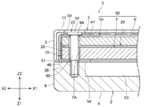
図6は、図3の切断線B−Bで切断した切断面を示す断面図である。LED基板35には、LED光源8が実装されている。そして、LED基板35の回路接続部37を光遮蔽フレーム10に設けられた孔部40に挿入し、光遮蔽フレーム35の下板部41の裏面側に沿わせ、フレーム9側から光遮蔽フレーム10の下板部41、LED基板35の回路接続部37の順に積み重ねる。そして、固定部材であるネジ21を回路接続部37と下板部41の共通位置に設けられた貫通孔から挿入し、フレーム9の外周枠部30に固定する。この際、ネジ21による固定前に反射板29と導光板7をフレーム9と光遮蔽部46の間に配設しておく。なお、ネジ軸部55の先端部は、フレーム9を貫通しない。   6 is a cross-sectional view showing a cut surface taken along the cutting line BB in FIG. An LED light source 8 is mounted on the LED substrate 35. Then, the circuit connecting portion 37 of the LED substrate 35 is inserted into the hole 40 provided in the light shielding frame 10, and along the back side of the lower plate portion 41 of the light shielding frame 35, the light shielding frame 10 from the frame 9 side. The lower plate portion 41 and the circuit connection portion 37 of the LED substrate 35 are stacked in this order. Then, the screw 21 that is a fixing member is inserted from a through hole provided at a common position of the circuit connecting portion 37 and the lower plate portion 41 and fixed to the outer peripheral frame portion 30 of the frame 9. At this time, the reflecting plate 29 and the light guide plate 7 are disposed between the frame 9 and the light shielding portion 46 before being fixed by the screw 21. Note that the tip end portion of the screw shaft portion 55 does not penetrate the frame 9.

前述したように、LED光源8と端面19に近づく方向の距離は、凸部20の端面19からの位置で規制される。また、LED基板35のLED光源8が実装される基板側部36は、フレーム9の側部45で基板側部36の左方への移動が規制される。一方、LED基板35の前後方向の位置は、光遮蔽フレーム10に設けられた孔部40によって規制される(図10参照)。なお、LED基板35の位置を規制する規制軸をフレーム9に設け、回路接続部37に規制軸を挿通する孔を設けるようにしてもよい。このように、フレーム9、光遮蔽フレーム10、LED光源8を含むLED基板35がネジ21で一体化された構成を光源ユニット50とする。なお、光源ユニット50は、導光板7および反射板29を含む。   As described above, the distance in the direction approaching the LED light source 8 and the end surface 19 is regulated by the position of the convex portion 20 from the end surface 19. Further, the board side portion 36 on which the LED light source 8 of the LED board 35 is mounted is restricted from moving to the left of the board side portion 36 by the side portion 45 of the frame 9. On the other hand, the position of the LED substrate 35 in the front-rear direction is regulated by the hole 40 provided in the light shielding frame 10 (see FIG. 10). A restriction shaft that restricts the position of the LED substrate 35 may be provided in the frame 9, and a hole through which the restriction shaft is inserted may be provided in the circuit connection portion 37. In this way, a configuration in which the frame 9, the light shielding frame 10, and the LED substrate 35 including the LED light source 8 are integrated with the screws 21 is referred to as a light source unit 50. The light source unit 50 includes the light guide plate 7 and the reflection plate 29.

LED基板35と接続基板38の電気的接続がハンダ固定の場合には、LED基板35に接続基板38を接続した状態で前述したようにネジ21によってフレーム9に固定する。ネジ21を締め付けた後に、保持ケース3を光源ユニット50に取り付けるが、保持ケース3の周縁部11には、ネジ頭部56の逃げ孔57が設けられている。ネジ21の頭部56は、保持ケース3の周縁部11から外面側(裏面側)に突出させない。   When the electrical connection between the LED substrate 35 and the connection substrate 38 is fixed by soldering, the LED substrate 35 is fixed to the frame 9 with the screws 21 as described above with the connection substrate 38 connected to the LED substrate 35. After tightening the screw 21, the holding case 3 is attached to the light source unit 50, and a clearance hole 57 for the screw head 56 is provided in the peripheral portion 11 of the holding case 3. The head portion 56 of the screw 21 is not projected from the peripheral edge portion 11 of the holding case 3 to the outer surface side (back surface side).

図7は、図3の切断線C−Cで切断した切断面を示す断面図である。ここでは、光源ユニット50を、拡散板2に固定する構造について説明する。光源ユニット50は、図6に示したように、フレーム9、光遮蔽フレーム10、およびLED光源8を含むLED基板35が固定部材であるネジ22で一体化された構成となっている。光源ユニット50は、光遮蔽フレーム10の下板部41の貫通孔、フレーム9に設けられた貫通孔Aおよび導光体7に設けられた貫通孔7Aにネジ22のネジ軸部60を挿入し、拡散板2の凸条部26に固定される。保持ケース3の周縁部11には、ネジ22のネジ頭部58の逃げ孔59が設けられ、ネジ頭部58は、保持ケース3の周縁部11から外面側(裏面側)に突出させないようにしている。   7 is a cross-sectional view showing a cut surface taken along the cutting line CC in FIG. Here, a structure for fixing the light source unit 50 to the diffusion plate 2 will be described. As shown in FIG. 6, the light source unit 50 has a configuration in which the frame 9, the light shielding frame 10, and the LED substrate 35 including the LED light source 8 are integrated with screws 22 as fixing members. The light source unit 50 inserts the screw shaft portion 60 of the screw 22 into the through hole of the lower plate portion 41 of the light shielding frame 10, the through hole A provided in the frame 9, and the through hole 7 A provided in the light guide 7. The ridges 26 of the diffusion plate 2 are fixed. A clearance hole 59 of the screw head 58 of the screw 22 is provided in the peripheral edge 11 of the holding case 3 so that the screw head 58 does not protrude from the peripheral edge 11 of the holding case 3 to the outer surface side (back surface side). ing.

なお、導光板7に設けられた貫通孔7Aおよびフレーム9に設けられた貫通孔9Aと、ネジ22のネジ軸部60の間には、拡散板2と導光板7とフレーム9の温度変化による伸縮の差を吸収できる程度の隙間が設けられている。前述したように、拡散板2および導光板7は、アクリル系樹脂で成形されていて、フレーム9は、アルミニウム板で成形されている。アクリル系樹脂の熱膨張率は、アルミニウムに対して約3倍である。したがって、温度変化によって、拡散板2および導光体7と、フレーム9の伸縮量が異なり、温度変化に伴い照明モジュール1が反ってしまうことが考えられる。そこで、導光板7に設けられた貫通孔7Aおよびフレーム9に設けられた貫通孔9Aと、ネジ22のネジ軸部60の間に、この伸縮量の差を吸収できる程度の隙間を設けている。   In addition, between the through hole 7A provided in the light guide plate 7 and the through hole 9A provided in the frame 9 and the screw shaft portion 60 of the screw 22, the temperature of the diffusion plate 2, the light guide plate 7, and the frame 9 is changed. A gap that can absorb the difference in expansion and contraction is provided. As described above, the diffusion plate 2 and the light guide plate 7 are formed of an acrylic resin, and the frame 9 is formed of an aluminum plate. The thermal expansion coefficient of acrylic resin is about 3 times that of aluminum. Therefore, it is conceivable that the expansion and contraction amounts of the diffusion plate 2 and the light guide 7 and the frame 9 differ depending on the temperature change, and the illumination module 1 warps with the temperature change. Therefore, a gap is provided between the through hole 7A provided in the light guide plate 7 and the through hole 9A provided in the frame 9 and the screw shaft portion 60 of the screw 22 so as to absorb this difference in expansion and contraction. .

また、ネジ22のネジ軸部60の先端部は、拡散板2の凸条部26内で第1光入射面53よりも第2光入射面51側になるような長さを有している。図7では、ネジ軸部60の先端部は、第1光入射面53のほぼ延長線上にあるが、ネジの固定強度が得られる範囲で、第2光入射面51側になるようなネジ軸部長さにすることが好ましい。そうすることによって、拡散板2の外周側面6と内側側面54の間で全反射しながら第2光出射面4から出射する光の経路(図5参照)は、ネジ軸60の先端部から拡散板2の第2光出射面4までの厚みが十分確保できるから、ネジ22によって妨げられることはない。   Further, the tip end portion of the screw shaft portion 60 of the screw 22 has such a length that it is closer to the second light incident surface 51 side than the first light incident surface 53 in the protruding strip portion 26 of the diffusion plate 2. . In FIG. 7, the tip of the screw shaft portion 60 is substantially on the extension line of the first light incident surface 53, but the screw shaft is located on the second light incident surface 51 side within a range where the fixing strength of the screw can be obtained. It is preferable to set the length. By doing so, the path (see FIG. 5) of the light emitted from the second light emitting surface 4 while being totally reflected between the outer peripheral side surface 6 and the inner side surface 54 of the diffusing plate 2 is diffused from the tip of the screw shaft 60. Since a sufficient thickness up to the second light exit surface 4 of the plate 2 can be secured, the screws 22 are not hindered.

一方、導光板7には、ネジ挿通用に複数の貫通孔7Aが設けられている。導光板7は、ほぼ全体が光の経路となっているので、貫通孔7Aが光の経路を妨げることも考えられる。しかし、前述したように、導光板7では、左辺側では右辺側からの光で明るさを補完し、右辺側では左辺側からの光で明るさを補完するようになっていて、前辺側および後辺側でも同様に相互に明るさを補完するようになっていて、貫通孔7Aは光の経路を妨げない。   On the other hand, the light guide plate 7 is provided with a plurality of through holes 7A for screw insertion. Since almost the entire light guide plate 7 serves as a light path, the through hole 7 </ b> A may prevent the light path. However, as described above, in the light guide plate 7, brightness is complemented with light from the right side on the left side, and brightness is complemented with light from the left side on the right side. Similarly, the rear sides also complement each other in brightness, and the through hole 7A does not hinder the light path.

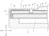
図8は、図3の切断線D−Dで切断した切断面を示す断面図で、LED基板35の回路接続部37を保持ケース3とフレーム9の間に介在する位置の固定構造を示す。図6および図7で説明したように、拡散板2、導光板7、反射板29、光遮蔽フレーム10、およびLED基板35(LED光源8付き)は、ネジ21、ネジ22で一体化されている。この一体化された状態で、保持ケース3は、固定部材であるネジ23によってフレーム9の外周枠部30に固定される。ネジ23による固定は、保持ケース3の溝部24内で行われる。ネジ23のネジ頭部61は、保持ケース3の周縁部11から外面側(裏面側)に突出しない。また、ネジ軸部62の先端部は、フレーム9を貫通しない。   FIG. 8 is a cross-sectional view showing a cut surface cut along the cutting line DD in FIG. 3 and shows a fixing structure at a position where the circuit connecting portion 37 of the LED substrate 35 is interposed between the holding case 3 and the frame 9. As described with reference to FIGS. 6 and 7, the diffusion plate 2, the light guide plate 7, the reflection plate 29, the light shielding frame 10, and the LED substrate 35 (with the LED light source 8) are integrated by screws 21 and screws 22. Yes. In this integrated state, the holding case 3 is fixed to the outer peripheral frame portion 30 of the frame 9 by screws 23 which are fixing members. Fixing with the screw 23 is performed in the groove 24 of the holding case 3. The screw head 61 of the screw 23 does not protrude from the peripheral edge 11 of the holding case 3 to the outer surface side (back surface side). Further, the tip end portion of the screw shaft portion 62 does not penetrate the frame 9.

図9は、保持ケース3とフレーム9の間にLED基板35を介在させない位置の固定構造を示す断面図である。このような位置では、保持ケース3は、溝部24の形成位置でフレーム9の外周枠部30に直接固定される。したがって、図9に示す固定構造では、図8に示した固定構造よりも、周縁部11の厚みがLED基板35の厚み分薄くなる。なお、ネジ23のネジ頭部61は、保持ケース3の周縁部11から外面側(裏面側)に突出させないようにしている。また、ネジ23のネジ軸部62の先端部は、フレーム9を貫通しない。   FIG. 9 is a cross-sectional view showing a fixing structure at a position where the LED substrate 35 is not interposed between the holding case 3 and the frame 9. In such a position, the holding case 3 is directly fixed to the outer peripheral frame portion 30 of the frame 9 at the position where the groove portion 24 is formed. Therefore, in the fixing structure shown in FIG. 9, the peripheral portion 11 is thinner than the fixing structure shown in FIG. 8 by the thickness of the LED substrate 35. Note that the screw head 61 of the screw 23 is not projected from the peripheral edge 11 of the holding case 3 to the outer surface side (back surface side). Further, the tip end portion of the screw shaft portion 62 of the screw 23 does not penetrate the frame 9.

一つの照明モジュール1において、図8および図9で示した固定構造が混在する。ここで、LED基板35は、フレキシブル基板であって、厚みが約0.15mmであり、回路接続部37は、フレーム9の溝部24の断面形状に倣って容易に変形可能である。一方、保持ケース3の厚みは約0.5mmであり、平面積に対しては極めて薄く、しかも上記2通りの固定部の距離を厚み差に対して大きくしていることで容易に撓むことが可能となっている。したがって、LED基板35を介在させて固定する位置と、LED基板を介在させずに固定する位置において、保持ケース3を裏面側からみても変形の差は認識できない程度の変形である。また、フレーム9は、保持ケース3に対して剛性があり変形しないので、導光板7および拡散板2における光の経路に影響を与えることはない。   In one lighting module 1, the fixing structures shown in FIGS. 8 and 9 are mixed. Here, the LED substrate 35 is a flexible substrate and has a thickness of about 0.15 mm, and the circuit connection portion 37 can be easily deformed following the cross-sectional shape of the groove portion 24 of the frame 9. On the other hand, the thickness of the holding case 3 is about 0.5 mm, is extremely thin with respect to the flat area, and can be easily bent by increasing the distance between the two fixing portions with respect to the thickness difference. Is possible. Accordingly, the deformation is such that the difference in deformation cannot be recognized even when the holding case 3 is viewed from the back side at the position where the LED substrate 35 is fixed and the position where the LED substrate 35 is fixed without being interposed. Further, since the frame 9 is rigid with respect to the holding case 3 and does not deform, it does not affect the light path in the light guide plate 7 and the diffusion plate 2.

前述したように、ネジ21、ネジ22およびネジ23の各ネジ頭部は、保持ケース3の周縁部11の外面側(裏面側)に突出しない構造としている。このようにすれば、照明モジュール1を裏面側から見たときにすっきりした外観が得られると共に、照明モジュール1を壁などに装着する際、固定部材であるネジが邪魔になることがない。   As described above, each screw head of the screw 21, the screw 22, and the screw 23 has a structure that does not protrude to the outer surface side (back surface side) of the peripheral edge portion 11 of the holding case 3. In this way, a clean appearance can be obtained when the illumination module 1 is viewed from the back side, and the screws that are fixing members do not get in the way when the illumination module 1 is mounted on a wall or the like.

次に、LED基板35と接続基板38の接続構造、および厚み方向の配置構造について説明する。   Next, the connection structure of the LED substrate 35 and the connection substrate 38 and the arrangement structure in the thickness direction will be described.

図10は、LED基板35と接続基板38の接続構造の一部を示す図であり、上段の(A)は、照明モジュール1を裏面側から見た斜視図、(A)の下段左方の(B)は、(A)の切断線D−Dで切断した切断面を示す断面図、(B)の右方の(C)は、(A)の切断線E−Eで切断した切断面を示す断面図である。図10(A)に示すように、LED基板35は、光遮蔽フレーム10に設けられた孔部40に回路接続部37が挿通され、回路接続部37は、フレーム9の裏面に沿って接続基板38との交差位置まで延長されている。LED基板35の一方の面(裏面35Aとする)および他方の面(表面35Bとする)には、不図示の配線層が形成されている。裏面35A側には、LED光源8が実装されている。裏面35A側の配線層には、LED光源8を実装するための配線が形成される。また、表面35Bの回路接続部37にも不図示の配線層が形成されている。表面35B側の配線層には、接続基板38と電気的接続を行うための配線が形成されている。裏面35A側の配線層と表面35B側の配線層は、スルーホールなどで接続されている。   FIG. 10 is a view showing a part of the connection structure of the LED board 35 and the connection board 38, and (A) in the upper stage is a perspective view of the illumination module 1 as viewed from the back side, and (A) is on the left side of the lower stage. (B) is sectional drawing which shows the cut surface cut | disconnected by the cutting line DD of (A), (C) of the right side of (B) is the cut surface cut | disconnected by the cutting line EE of (A). FIG. As shown in FIG. 10A, the LED board 35 has a circuit connection portion 37 inserted through a hole 40 provided in the light shielding frame 10, and the circuit connection portion 37 is connected to the connection substrate along the back surface of the frame 9. 38 is extended to the crossing position. A wiring layer (not shown) is formed on one surface (referred to as a back surface 35A) and the other surface (referred to as a front surface 35B) of the LED substrate 35. The LED light source 8 is mounted on the back surface 35A side. Wiring for mounting the LED light source 8 is formed on the wiring layer on the back surface 35A side. A wiring layer (not shown) is also formed on the circuit connection portion 37 on the surface 35B. In the wiring layer on the surface 35B side, wiring for making electrical connection with the connection substrate 38 is formed. The wiring layer on the back surface 35A side and the wiring layer on the front surface 35B side are connected by a through hole or the like.

LED基板35の回路接続部37は、先端部が接続基板38と重ね合わされて接続手段で電気的に接続される。接続基板38の裏面38Aには、不図示の配線層が形成されている。この配線層には、LED基板35(LED光源8)と回路部39を接続する配線と、外部電源と回路部39を接続する配線などが形成されている。図10(B)に示すように、LED基板35の表面35Bに設けられた配線層と接続基板38の配線層の接続は、接続手段であるハンダ64によって電気的に接続される。なお、ハンダ接続部の保護と絶縁を兼ねて、図中、2点鎖線で示した領域に樹脂盛り部(ポッティング)65が設けられる。なお、ハンダ接続部と樹脂盛り部を含めて接続部66とする。接続部66は、フレーム9の外周枠部30の内側(開口部31内)に突出するように配置される。つまり、接続部66は、フレーム9と交差しない位置に配置される。   The circuit connection portion 37 of the LED substrate 35 is electrically connected by a connection means with the tip portion overlapped with the connection substrate 38. A wiring layer (not shown) is formed on the back surface 38 </ b> A of the connection substrate 38. In this wiring layer, wiring for connecting the LED substrate 35 (LED light source 8) and the circuit unit 39, wiring for connecting the external power source and the circuit unit 39, and the like are formed. As shown in FIG. 10B, the connection between the wiring layer provided on the surface 35B of the LED substrate 35 and the wiring layer of the connection substrate 38 is electrically connected by solder 64 which is a connection means. In addition, in the drawing, a resin heap (potting) 65 is provided in a region indicated by a two-dot chain line in order to double the protection and insulation of the solder connection portion. In addition, it is set as the connection part 66 including a solder connection part and the resin pile part. The connecting portion 66 is disposed so as to protrude inside the outer peripheral frame portion 30 of the frame 9 (inside the opening 31). That is, the connecting portion 66 is disposed at a position that does not intersect the frame 9.

接続基板38の裏面38Aには、回路部39が周知の接合手段によって固定される。回路部39は、LED光源8の点灯制御を行うICチップや抵抗素子などの回路素子を有している。これらの回路素子は、樹脂モールドなどで1パッケージ化して接続基板38に接合してもよく、回路素子単体で接続基板38に接合してもよい。回路部39が1パッケージ化されている場合には、接続基板38に設けられた配線に対応させるように回路部39の端子を配置し、ハンダまたは導電性接着剤などの接合手段で電気的に接続する。また、回路素子単体で接合する場合には、接合後、各回路素子を樹脂モールドなどで覆うことが好ましい。LED基板35と回路部39は、接続基板38の裏面38Aに設けられた配線層によって接続される。つまり、LED光源8と回路部39が電気的に接続されている。なお、接続基板38には、不図示のリード線が接続されており、このリード線は、外部の電源部に接続され、回路部39に電力を供給できるようになっている。   The circuit portion 39 is fixed to the back surface 38A of the connection substrate 38 by a known joining means. The circuit unit 39 includes circuit elements such as an IC chip and a resistance element that perform lighting control of the LED light source 8. These circuit elements may be packaged in one package with a resin mold or the like and bonded to the connection substrate 38, or the circuit elements alone may be bonded to the connection substrate 38. When the circuit unit 39 is packaged in one package, the terminals of the circuit unit 39 are arranged so as to correspond to the wiring provided on the connection substrate 38, and are electrically connected by a bonding means such as solder or conductive adhesive. Connecting. Further, in the case of joining circuit elements alone, it is preferable to cover each circuit element with a resin mold or the like after joining. The LED substrate 35 and the circuit unit 39 are connected by a wiring layer provided on the back surface 38 </ b> A of the connection substrate 38. That is, the LED light source 8 and the circuit unit 39 are electrically connected. Note that a lead wire (not shown) is connected to the connection substrate 38, and the lead wire is connected to an external power supply unit so that power can be supplied to the circuit unit 39.

回路部39は、図10(C)に示すように、接続基板38の裏面38Aに電気的に接続され、フレーム9の外周枠部30と開口部31を跨ぐような位置に配設されている。フレーム9が無い場合には、回路部39は、たとえば図中39Aで示す位置となる。回路部39を、フレーム9に当接させることで、回路部39とフレーム9との交差量H分だけ接続基板38は保持ケース3側に寄せられる。つまり、LED基板35が撓められ、その弾性力と接続基板38の重量の合計が、回路部39とフレーム9の接触圧となる。回路部39は、LED光源8を点灯することで発熱する。しかし、回路部39と熱伝導率が高いフレーム9を当接させることにより、回路部39の熱を、フレーム9から保持ケース3に伝達し、保持ケース3に接触している保持ケース3から逃がすようにしている。   As shown in FIG. 10C, the circuit portion 39 is electrically connected to the back surface 38 </ b> A of the connection substrate 38, and is disposed at a position that straddles the outer peripheral frame portion 30 and the opening portion 31 of the frame 9. . When there is no frame 9, the circuit unit 39 is at a position indicated by 39A in the figure, for example. By bringing the circuit portion 39 into contact with the frame 9, the connection substrate 38 is brought closer to the holding case 3 side by the amount of intersection H between the circuit portion 39 and the frame 9. That is, the LED substrate 35 is bent, and the total of the elastic force and the weight of the connection substrate 38 becomes the contact pressure between the circuit portion 39 and the frame 9. The circuit unit 39 generates heat when the LED light source 8 is turned on. However, by bringing the circuit portion 39 and the frame 9 having high thermal conductivity into contact with each other, the heat of the circuit portion 39 is transmitted from the frame 9 to the holding case 3 and is released from the holding case 3 in contact with the holding case 3. I am doing so.

LED基板35には、裏面35Aおよび表面35B共に、LED光源8との接続部分および接続基板38との接続部分を除く領域全面に絶縁層を設けることが好ましい。また、接続基板38の裏面38A側においても、LED基板35との接続部分および回路部39との接続部分を除く全面に絶縁層を設けることが好ましい。絶縁層を設けることで、他の部材との接触によるショートを防止できる。また、照明モジュール1の使用環境によって結露する場合が考えられるが、そのような場合においても、絶縁層を設けることで結露によるショートを防止できる。   It is preferable to provide an insulating layer on the entire surface of the LED substrate 35 except for the connection portion with the LED light source 8 and the connection portion with the connection substrate 38 on both the back surface 35A and the front surface 35B. Further, it is preferable to provide an insulating layer on the entire back surface of the connection substrate 38 except for the connection portion with the LED substrate 35 and the connection portion with the circuit portion 39. By providing the insulating layer, a short circuit due to contact with other members can be prevented. Moreover, although the case where condensation forms by the use environment of the illumination module 1 is considered, the short circuit by condensation can be prevented by providing an insulating layer also in such a case.

図10では、LED基板35と接続基板38との接続手段は、ハンダ64であるが、周知のフレキシブル基板用コネクタを用いて接続することが可能である。図示は省略するが、図10を参照しながら説明する。フレキシブル基板用コネクタは、接続基板38の裏面38Aの所定位置に実装される。LED基板35の先端部をフレキシブル基板用コネクタに差し込めば、LED基板35と接続基板38の電気的接続が可能となる。なお、LED基板35のフレキシブル基板用コネクタへの挿入部に、補強用の基板を設けておけば、フレキシブル基板用コネクタとの接続の信頼性を高められる。フレキシブル基板用コネクタは、接続部66と同様に、フレーム9の開口部31内に、外周枠部30と交差しないように配置される。   In FIG. 10, the connection means between the LED substrate 35 and the connection substrate 38 is the solder 64, but it can be connected using a known flexible substrate connector. Although not shown, the description will be given with reference to FIG. The flexible board connector is mounted at a predetermined position on the back surface 38 </ b> A of the connection board 38. If the tip of the LED substrate 35 is inserted into the flexible substrate connector, the LED substrate 35 and the connection substrate 38 can be electrically connected. In addition, if the board | substrate for reinforcement is provided in the insertion part to the connector for flexible substrates of the LED board 35, the reliability of a connection with the connector for flexible substrates can be improved. The flexible board connector is arranged in the opening 31 of the frame 9 so as not to intersect with the outer peripheral frame portion 30, similarly to the connection portion 66.

以上説明した照明モジュール1は、第1光出射面32を有する導光板7と、光を発するLED光源8を有している。また、照明モジュール1は、導光板7の第1光出射面32の側に配置され、第1光出射面32から出射した光が入射する第1光入射面53と、第1光入射面53から入射した光が出射する第2光出射面4を有する拡散板2と、導光板7の第1光出射面32に対して反対側の面に沿って配設される反射板29と、反射板29の裏面側に配置される枠形状のフレーム9と、LED光源8の点灯制御を行う回路部39を有している。拡散板2は、導光板の周縁部27から出射する光が入射する第2光入射面51を有する。また、周縁部27と第2光入射面51との間には、周縁部27から出射した光が第2光入射面51に入射する光量を制限する光遮蔽フレーム10を備えている。そして、LED光源8が実装されるLED基板35と、回路部39が実装される接続基板38を電気的に接続する接続部66を、フレーム9の外周枠部30の内側空間内で導光板7側に突出するように配設している。   The illumination module 1 described above includes the light guide plate 7 having the first light emission surface 32 and the LED light source 8 that emits light. The illumination module 1 is arranged on the first light exit surface 32 side of the light guide plate 7, and a first light entrance surface 53 on which light emitted from the first light exit surface 32 is incident, and the first light entrance surface 53. A diffuser plate 2 having a second light exit surface 4 through which light incident from the light exits, a reflector 29 disposed along a surface opposite to the first light exit surface 32 of the light guide plate 7, and a reflection A frame-shaped frame 9 disposed on the back side of the plate 29 and a circuit unit 39 for controlling the lighting of the LED light source 8 are provided. The diffusion plate 2 has a second light incident surface 51 on which light emitted from the peripheral portion 27 of the light guide plate enters. A light shielding frame 10 is provided between the peripheral edge 27 and the second light incident surface 51 to limit the amount of light emitted from the peripheral edge 27 and incident on the second light incident surface 51. The light guide plate 7 is connected to the LED board 35 on which the LED light source 8 is mounted and the connection part 66 for electrically connecting the connection board 38 on which the circuit part 39 is mounted in the inner space of the outer peripheral frame part 30 of the frame 9. It arrange | positions so that it may protrude to the side.

このような構成にすることで、LED光源8から導光板7に入射した光は、導光板7の第1光出射面32から拡散板2の第1光入射面53に入射し、拡散板2の第2光出射面4から出射される。また、導光板7の第1光出射面32の周縁部27から拡散板2の第2光入射面51に入射した光は、主として、第2光出射面53の周縁部から出射される。したがって、第2光出射面4からLED光源8が点光源のように見えることがなく、拡散板2の第2光出射面4の全面の明るさを均斉化させることができる。拡散板2は、光散乱粒子を含有しているため、第2光出射面4から出射する光は、第2光出射面4のどの方向から見ても光の強さと色調(波長)に差がない照明モジュール1を提供できる。   With this configuration, the light incident on the light guide plate 7 from the LED light source 8 enters the first light incident surface 53 of the diffusion plate 2 from the first light emission surface 32 of the light guide plate 7, and the diffusion plate 2. Is emitted from the second light exit surface 4. Further, light that has entered the second light incident surface 51 of the diffusion plate 2 from the peripheral portion 27 of the first light emitting surface 32 of the light guide plate 7 is mainly emitted from the peripheral portion of the second light emitting surface 53. Therefore, the LED light source 8 does not look like a point light source from the second light emitting surface 4, and the brightness of the entire surface of the second light emitting surface 4 of the diffusion plate 2 can be made uniform. Since the diffusing plate 2 contains light scattering particles, the light emitted from the second light exit surface 4 is different in light intensity and color tone (wavelength) when viewed from any direction of the second light exit surface 4. It is possible to provide the lighting module 1 without the above.

一方、LED基板35と接続基板38との接続部66を、フレーム9の外周枠部30の内側空間内(開口部31内)に突出させることで、照明モジュール1の総厚み(保持ケース3の内側部分12と拡散板2の厚み)を薄くすることができる。   On the other hand, the connection portion 66 between the LED substrate 35 and the connection substrate 38 protrudes into the inner space (inside the opening 31) of the outer peripheral frame portion 30 of the frame 9, so that the total thickness of the lighting module 1 (the holding case 3 The thickness of the inner portion 12 and the diffusion plate 2) can be reduced.

また、導光板7は、LED光源8が配列されると共に、LED光源8が発する光が入射される端面19と、端面19の周縁部27に対向する位置に設けられ、導光板7側に突出し第2光入射面27を備える凸条部26を有している。また、照明モジュール1は、導光板7と、LED基板35およびフレーム9などを拡散板2との間に収容する保持ケース3を有し、保持ケース3の外周側面5は、拡散板2の外周側面6と同一面内に配置するか、または拡散板2の外周側面6より内側に配置している。このように構成すれば、照明モジュール1を上方から見たときに、保持ケース3が額縁のように見えてしまうことがない。また、保持ケース3の周縁部11の厚みを、周縁部11の内側部分(照明モジュール1の内側部分)よりも薄くしているので、照明モジュール1を斜め上方から見ても、保持ケース3の薄い部分である外周側面6しか見えないので、薄く感じさせることができる。   The light guide plate 7 is provided with LED light sources 8 arranged at positions facing the end surface 19 where the light emitted from the LED light source 8 is incident and the peripheral portion 27 of the end surface 19, and protrudes toward the light guide plate 7 side. It has a ridge 26 with a second light incident surface 27. The illumination module 1 also has a holding case 3 that houses the light guide plate 7, the LED substrate 35, the frame 9, and the like between the diffusion plate 2, and the outer peripheral side surface 5 of the holding case 3 is the outer periphery of the diffusion plate 2. It arrange | positions in the same surface as the side surface 6, or has arrange | positioned inside the outer peripheral side surface 6 of the diffusion plate 2. FIG. If comprised in this way, when the illumination module 1 is seen from upper direction, the holding | maintenance case 3 will not look like a frame. Moreover, since the thickness of the peripheral part 11 of the holding case 3 is made thinner than the inner part of the peripheral part 11 (inner part of the illumination module 1), even if the illumination module 1 is viewed obliquely from above, Since only the outer peripheral side surface 6 which is a thin part can be seen, it can be made to feel thin.

また、光遮蔽フレーム10は、側部45と、側部45の一方の端部から延在される上板部である光遮蔽部46と、他方の端部から延在される下板部41を有し、LED基板35は、LED光源8が実装される基板側部36と、基板側部36から下板部41に重なるように延在される回路接続部37を有している。そして、光遮蔽部46と下板部41の間に、導光板7とLED基板35とフレーム9を重ねて配置すると共に、回路接続部37と下板部41の共通位置に設けられた貫通孔に挿入されるネジ21で、フレーム9の外周枠部30に固定して光源ユニット50を構成している。光源ユニット50は、下板部41、フレーム9および導光板7の共通位置に設けられた貫通孔に挿入されるネジ22で、拡散板2の凸条部26に固定される。保持ケース3は、保持ケース3の周縁部11に形成された溝部24内の貫通孔に挿入されるネジ23でフレーム9の外周枠部30に固定する。   The light shielding frame 10 includes a side portion 45, a light shielding portion 46 that is an upper plate portion that extends from one end portion of the side portion 45, and a lower plate portion 41 that extends from the other end portion. The LED substrate 35 includes a substrate side portion 36 on which the LED light source 8 is mounted, and a circuit connection portion 37 extending from the substrate side portion 36 so as to overlap the lower plate portion 41. The light guide plate 7, the LED substrate 35, and the frame 9 are disposed so as to overlap each other between the light shielding portion 46 and the lower plate portion 41, and a through hole provided at a common position of the circuit connection portion 37 and the lower plate portion 41. The light source unit 50 is configured by being fixed to the outer peripheral frame portion 30 of the frame 9 with screws 21 inserted into the frame 9. The light source unit 50 is fixed to the convex portion 26 of the diffusion plate 2 with screws 22 inserted into through holes provided at a common position of the lower plate portion 41, the frame 9 and the light guide plate 7. The holding case 3 is fixed to the outer peripheral frame portion 30 of the frame 9 with a screw 23 inserted into a through hole in a groove portion 24 formed in the peripheral edge portion 11 of the holding case 3.

このように、照明モジュール1は、照明モジュール1の内側より薄い周縁部において、光源ユニット50、拡散板2、保持ケース3の順にネジ21,22,23によって、各ネジ頭部が、保持ケース3の周縁部11の外面側よりも突出しないように固定することで、薄型化を実現することが可能となる。照明モジュール1を裏面側から見たときにすっきりした外観が得られると共に、照明モジュール1を壁などに装着する際、固定部材であるネジが邪魔になることがない。さらに、上記各部の固定手段がネジ21,22,23で行うことが可能になっていることから、組立性および分解性が優れた照明モジュール1を実現できる。   As described above, the lighting module 1 has the screw heads of the holding case 3 at the peripheral edge thinner than the inner side of the lighting module 1 by the screws 21, 22 and 23 in the order of the light source unit 50, the diffusion plate 2, and the holding case 3. By fixing so that it may not protrude rather than the outer surface side of the peripheral part 11, it becomes possible to implement | achieve thickness reduction. When the illumination module 1 is viewed from the back side, a clean appearance is obtained, and when the illumination module 1 is mounted on a wall or the like, a screw as a fixing member does not get in the way. Furthermore, since the fixing means for each part can be performed by the screws 21, 22, and 23, the illumination module 1 that is excellent in assembling and disassembling can be realized.

また、固定部材であるネジ21、ネジ22およびネジ23は、LED光源8が出射した光が第2光出射面53から出射するまでの光の経路を妨げない位置に配置されている。このようにすることで、照明モジュール1を薄型化し、ネジ21,22,23を設ける構造であっても光の経路を妨げないことから、LED光源8から出射される光を効率よく第2光出射面53から出射させることができる。   Further, the screw 21, screw 22, and screw 23, which are fixing members, are arranged at positions that do not hinder the light path until the light emitted from the LED light source 8 is emitted from the second light emitting surface 53. By doing so, the illumination module 1 is thinned and the screws 21, 22, and 23 are provided, so that the light path is not obstructed. Therefore, the light emitted from the LED light source 8 is efficiently second light. The light can be emitted from the emission surface 53.

また、照明モジュール1は、ネジ22が挿通される導光板7およびフレーム9各々に設けられた貫通孔7A,9Aと、ネジ22のネジ軸部60の間に、拡散板2と導光板7とフレーム9の温度変化に伴う伸縮の差を吸収できる程度の隙間を設けている。   Further, the illumination module 1 includes the diffusion plate 2 and the light guide plate 7 between the through holes 7A and 9A provided in the light guide plate 7 and the frame 9 through which the screw 22 is inserted, and the screw shaft portion 60 of the screw 22, respectively. A gap is provided so as to absorb the difference in expansion and contraction accompanying the temperature change of the frame 9.

前述したように、拡散板2および導光板7は、アクリル系樹脂で成形されていて、フレーム9は、アルミニウム板で成形されている。アクリル系樹脂とアルミニウムでは熱膨張率が異なり、温度変化によって、拡散板2および導光体7と、フレーム9の伸縮量が異なり、温度変化に伴い照明モジュール1が反ってしまうことが考えられる。そこで、導光板7に設けられた貫通孔7Aおよびフレーム9に設けられた貫通孔9Aと、ネジ22のネジ軸部60の間に、この温度変化による伸縮差を吸収できる程度の隙間を設けているので、この隙間によって伸縮の差を吸収できることから、照明モジュール1が反ってしまうことを防止できるようにしている。   As described above, the diffusion plate 2 and the light guide plate 7 are formed of an acrylic resin, and the frame 9 is formed of an aluminum plate. The acrylic resin and aluminum have different coefficients of thermal expansion, and the expansion and contraction amounts of the diffusion plate 2 and the light guide 7 and the frame 9 differ depending on the temperature change, and the illumination module 1 may be warped as the temperature changes. Therefore, a gap is provided between the through hole 7A provided in the light guide plate 7 and the through hole 9A provided in the frame 9 and the screw shaft portion 60 of the screw 22 so as to absorb the expansion / contraction difference due to the temperature change. Therefore, since the difference in expansion and contraction can be absorbed by this gap, the lighting module 1 can be prevented from warping.

また、照明モジュール1は、ネジ22のネジ軸部60の先端部を、拡散板2の凸条部26内で第1光入射面53より第2光入射面51側に配置している。このようにすれば、凸条部26内において、第2光入射面51から入射された光が、凸条部26の内側側面54と外周側面6の間を全反射しながら第2光出射面4に向かう経路を妨げられることなく、第2光出射面4から出射させる光量の均斉化を図ることができる。   Further, in the illumination module 1, the tip end portion of the screw shaft portion 60 of the screw 22 is disposed on the second light incident surface 51 side from the first light incident surface 53 in the convex portion 26 of the diffusion plate 2. In this way, the light incident from the second light incident surface 51 in the ridge 26 is totally reflected between the inner side surface 54 and the outer peripheral surface 6 of the ridge 26, and the second light exit surface. The amount of light emitted from the second light exit surface 4 can be leveled without being obstructed by the path toward 4.

また、導光板7には、端面19からLED光源8の方向に突設された複数の凸部20が設けられ、隣り合う凸部20の間にLED光源8を配設すると共に、凸部20の先端面が基板側部36のLED光源8が実装される側の面に当接させている。   The light guide plate 7 is provided with a plurality of convex portions 20 protruding from the end surface 19 in the direction of the LED light source 8. The LED light source 8 is disposed between the adjacent convex portions 20, and the convex portion 20. Is in contact with the surface of the substrate side portion 36 on which the LED light source 8 is mounted.

LED光源8から導光板7の端面19に入射される光の強さは、LED光源8と端面19の距離に左右される。そこで、導光板7に設けられた凸部20の先端面を、LED基板35の基板側部36に当接させる。つまり、LED光源8と端面19の距離は、凸部20の先端面の端面19からの位置で規制される。また、LED基板35のLED光源8が実装される基板側部36は、フレーム9の側部45で基板側部36の左方への移動が規制される。このようにして、LED光源8と導光板7の端面19の距離がほぼ一定に保持されることで、端面19に入射される光の強さを、ほぼ一定となるように管理することが可能となる。   The intensity of light incident on the end surface 19 of the light guide plate 7 from the LED light source 8 depends on the distance between the LED light source 8 and the end surface 19. Therefore, the front end surface of the convex portion 20 provided on the light guide plate 7 is brought into contact with the substrate side portion 36 of the LED substrate 35. That is, the distance between the LED light source 8 and the end surface 19 is regulated by the position from the end surface 19 of the front end surface of the convex portion 20. Further, the board side portion 36 on which the LED light source 8 of the LED board 35 is mounted is restricted from moving to the left of the board side portion 36 by the side portion 45 of the frame 9. In this way, the distance between the LED light source 8 and the end face 19 of the light guide plate 7 is kept substantially constant, so that the intensity of light incident on the end face 19 can be managed to be substantially constant. It becomes.

また、保持ケース3とフレーム9は、熱伝導率が高い金属板で成形され、回路部39のフレーム9に対向する側の面を、フレーム9に当接させている。回路部39は、LED光源8を点灯することで発熱することがある。しかし、回路部39とアルミニウム製のフレーム9を当接させることにより、回路部39の熱がフレーム9に伝達する。フレーム9は、ネジ23によってアルミニウム製の保持ケース3に接触しているので、回路部39の熱はフレーム9を介して保持ケース3から逃がすことができるので、回路部39が高温になることを防止できる。   The holding case 3 and the frame 9 are formed of a metal plate having a high thermal conductivity, and the surface of the circuit portion 39 facing the frame 9 is brought into contact with the frame 9. The circuit unit 39 may generate heat when the LED light source 8 is turned on. However, the heat of the circuit unit 39 is transmitted to the frame 9 by bringing the circuit unit 39 and the aluminum frame 9 into contact with each other. Since the frame 9 is in contact with the aluminum holding case 3 by the screw 23, the heat of the circuit portion 39 can be released from the holding case 3 through the frame 9, so that the circuit portion 39 becomes hot. Can be prevented.

なお、本発明は前述の実施の形態に限定されるものではなく、本発明の目的を達成できる範囲での変形、改良等は本発明に含まれるものである。たとえば、前述した実施の形態では、LED基板35をフレキシブル基板とし、接続基板38をリジット基板として、両者を接続する構成としているが、LED基板35と接続基板38をフレキシブル基板で一体形成してもよい。   It should be noted that the present invention is not limited to the above-described embodiment, but includes modifications and improvements as long as the object of the present invention can be achieved. For example, in the above-described embodiment, the LED substrate 35 is a flexible substrate, the connection substrate 38 is a rigid substrate, and both are connected. However, the LED substrate 35 and the connection substrate 38 may be integrally formed of a flexible substrate. Good.

また、前述の照明モジュール1では、LED基板35の回路接続部37を、光遮蔽フレーム10に設けた孔部40に挿通して、光遮蔽フレーム10の下板部41に沿って延長しているが、LED基板35の回路接続部37を孔部40に挿通させずに、フレーム9と下板部41の間に配置する構造としてもよい。また、拡散板2の第2光入射面51と第1光入射面53とが、一体に連なる平面としてもよい。   In the illumination module 1 described above, the circuit connecting portion 37 of the LED substrate 35 is inserted through the hole 40 provided in the light shielding frame 10 and extends along the lower plate portion 41 of the light shielding frame 10. However, the circuit connection portion 37 of the LED substrate 35 may be disposed between the frame 9 and the lower plate portion 41 without being inserted into the hole portion 40. Further, the second light incident surface 51 and the first light incident surface 53 of the diffusing plate 2 may be a flat surface integrally connected.

また、前述の照明モジュール1では、第1の固定部材であるネジ21で、光源ユニット50を構成し、第2の固定部材であるネジ22で、光源ユニット50を拡散板2に固定している。しかし、ネジ22で、導光板7、反射板29、フレーム9、光遮蔽フレーム10およびLED基板35を重ねて拡散板2に固定する構造としてもよい。   In the illumination module 1 described above, the light source unit 50 is configured by the screws 21 that are the first fixing members, and the light source unit 50 is fixed to the diffusion plate 2 by the screws 22 that are the second fixing members. . However, the light guide plate 7, the reflection plate 29, the frame 9, the light shielding frame 10, and the LED substrate 35 may be overlapped and fixed to the diffusion plate 2 with the screws 22.

また、前述の照明モジュール1では、回路部39をフレーム9に当接させて、回路部39の温度上昇を抑える構造としているが、反射板29をアルミニウムなどの熱伝導率が高い材質とし、回路部39をフレーム9の開口部31内に配置し、回路部39を反射板29に当接させるようにしてもよい。また、回路部39と反射板29の間に、熱伝導体を介在させるようにしてもよい。   In the lighting module 1 described above, the circuit portion 39 is brought into contact with the frame 9 to suppress the temperature rise of the circuit portion 39. However, the reflecting plate 29 is made of a material having high thermal conductivity such as aluminum, and the circuit. The part 39 may be disposed in the opening 31 of the frame 9 so that the circuit part 39 is brought into contact with the reflecting plate 29. Further, a heat conductor may be interposed between the circuit unit 39 and the reflection plate 29.

1…照明モジュール
2…拡散板
3…保持ケース
4…第2光出射面
5…外周側面(保持ケースの)
6…外周側面(拡散板の)
7…導光板
7A…貫通孔
8…LED光源(光源)
9…フレーム
9A…貫通孔
10…光遮蔽フレーム
11…周縁部(保持ケースの)
12…内側部分(保持ケースの)
19…端面
20…凸部(導光板の)
21…ネジ
22…ネジ
23…ネジ
24…溝部(保持ケースの)
26…凸条部
27…周縁部(導光板の)
29…反射板
30…外周枠部(フレームの)
32…第1光出射面
35…LED基板
38…接続基板
39…回路部
41…下板部
46…光遮蔽部
50…光源ユニット
51…第2光入射面
53…第1光入射面
62…ネジ軸部
66…接続部
DESCRIPTION OF SYMBOLS 1 ... Illumination module 2 ... Diffuser 3 ... Holding case 4 ... 2nd light-projection surface 5 ... Outer peripheral side surface (of holding case)
6 ... Outer peripheral side (diffusion plate)
7 ... Light guide plate 7A ... Through hole 8 ... LED light source (light source)
DESCRIPTION OF SYMBOLS 9 ... Frame 9A ... Through-hole 10 ... Light shielding frame 11 ... Peripheral part (of holding case)
12 ... Inside part (of the holding case)
19 ... End face 20 ... Convex part (of light guide plate)
21 ... Screw 22 ... Screw 23 ... Screw 24 ... Groove (of the holding case)
26 ... ridge 27 ... peripheral part (of light guide plate)
29 ... Reflector 30 ... Outer frame (frame)
32 ... 1st light-projection surface 35 ... LED board 38 ... Connection board 39 ... Circuit part 41 ... Lower board part 46 ... Light shielding part 50 ... Light source unit 51 ... 2nd light-incidence surface 53 ... 1st light-incidence surface 62 ... Screw Shaft part 66 ... connection part

Claims (8)

第1光出射面を有する導光板と、
光を発する光源と、
前記導光板の前記第1光出射面の側に配置され、前記第1光出射面から出射した光が入射する第1光入射面と、当該第1光入射面から入射した光が出射する第2光出射面を有する拡散板と、
前記導光板の前記第1光出射面に対して反対側の面に沿って配設される枠形状のフレームと、
前記光源の点灯制御を行う回路部と、
を有し、
前記拡散板は、前記導光板側の周縁部から出射する光が入射する第2光入射面を有し、
前記周縁部と前記第2光入射面の間には、前記周縁部から出射した光が前記第2光入射面に入射する光量を制限する光遮蔽フレームが備えられ、
前記光源が実装される光源基板と、前記回路部が実装される接続基板を電気的に接続する接続部が、前記フレームの外周枠部の内側空間内で前記導光板側に突出するように配設されている、
ことを特徴とする照明モジュール。
A light guide plate having a first light exit surface;
A light source that emits light;
A first light incident surface that is disposed on the first light emitting surface side of the light guide plate and receives light emitted from the first light emitting surface, and a first light incident surface from which light incident from the first light incident surface is emitted. A diffuser having two light exit surfaces;
A frame-shaped frame disposed along a surface opposite to the first light exit surface of the light guide plate;
A circuit unit for controlling lighting of the light source;
Have
The diffusion plate has a second light incident surface on which light emitted from a peripheral portion on the light guide plate side is incident,
A light shielding frame is provided between the peripheral edge and the second light incident surface to limit the amount of light emitted from the peripheral edge to be incident on the second light incident surface.
A light source substrate on which the light source is mounted and a connection portion that electrically connects the connection substrate on which the circuit unit is mounted are arranged so as to protrude toward the light guide plate in the inner space of the outer peripheral frame portion of the frame. Has been established,
An illumination module characterized by that.
請求項1に記載の照明モジュールにおいて、
前記導光板は、前記光源が配列されると共に、前記光源が発する光が入射される端面と、前記端面の周縁部に対向する位置に設けられ、前記導光板側に突出し前記第2光入射面を備える凸条部を有し、
前記導光板と、前記光源基板および前記フレームなどを前記拡散板との間に収容するケース部材を有し、
前記ケース部材の外周側面は、前記拡散板の外周側面と同一面内に配置されるか、または前記拡散板の前記外周側面より内側に配置され、
前記ケース部材の周縁部の厚みは、当該周縁部の内側部分よりも薄くしている、
ことを特徴とする照明モジュール。
The lighting module according to claim 1,
The light guide plate is provided at a position facing an end surface on which light emitted from the light source is incident and a peripheral portion of the end surface, and protrudes toward the light guide plate, and the second light incident surface. Having a ridge with
A case member for accommodating the light guide plate, the light source substrate, the frame, and the like between the diffuser plate;
The outer peripheral side surface of the case member is arranged in the same plane as the outer peripheral side surface of the diffusion plate, or is arranged inside the outer peripheral side surface of the diffusion plate,
The thickness of the peripheral part of the case member is thinner than the inner part of the peripheral part,
An illumination module characterized by that.
請求項1または請求項2に記載の照明モジュールにおいて、
前記光遮蔽フレームは、側部と、当該側部の一方の端部から延在される上板部と、他方の端部から延在される下板部を有し、
前記光源基板は、前記光源が実装される基板側部と、前記基板側部から前記下板部に重なるように延在される回路接続部を有し、
前記上板部と前記下板部の間に、前記導光板と前記光源基板と前記フレームを重ねて配置すると共に、前記回路接続部と前記下板部の共通位置に設けられた貫通孔に挿入される第1のネジで、前記フレームの外周枠部に固定して光源ユニットを構成し、
前記光源ユニットは、前記下板部、前記フレームおよび前記導光体の共通位置に設けられた貫通孔に挿入される第2のネジで、前記拡散板の前記第2光入射面側に固定され、
前記ケース部材は、当該ケース部材に設けられた貫通孔に挿入される第3のネジで前記フレームの前記外周枠部に固定される、
ことを特徴とする照明モジュール。
The illumination module according to claim 1 or 2,
The light shielding frame has a side, an upper plate extending from one end of the side, and a lower plate extending from the other end,
The light source substrate includes a substrate side portion on which the light source is mounted, and a circuit connection portion that extends from the substrate side portion so as to overlap the lower plate portion,
The light guide plate, the light source substrate, and the frame are arranged to overlap between the upper plate portion and the lower plate portion, and inserted into a through hole provided at a common position of the circuit connection portion and the lower plate portion. The light source unit is configured by fixing to the outer peripheral frame portion of the frame with a first screw that is
The light source unit is fixed to the second light incident surface side of the diffusion plate by a second screw inserted into a through hole provided at a common position of the lower plate portion, the frame, and the light guide. ,
The case member is fixed to the outer peripheral frame portion of the frame with a third screw inserted into a through hole provided in the case member.
An illumination module characterized by that.
請求項3に記載の照明モジュールにおいて、
前記第1のネジ、前記第2のネジおよび前記第3のネジは、前記光源が出射した光が前記第2光出射面から出射するまでの光の経路を妨げない位置に配置されている、
ことを特徴とする照明モジュール。
The lighting module according to claim 3.
The first screw, the second screw, and the third screw are arranged at positions that do not hinder the light path from the light emitted by the light source until it is emitted from the second light emitting surface.
An illumination module characterized by that.
請求項3または請求項4に記載の照明モジュールにおいて、
前記第3のネジが挿通される前記導光板および前記フレーム各々に設けられた貫通孔と、前記第3のネジのネジ軸部の間に、前記拡散板と前記導光板と前記フレームの温度変化に伴う伸縮の差を吸収できる程度の隙間が設けられている、
ことを特徴とする照明モジュール
The lighting module according to claim 3 or 4,
Temperature change of the diffusion plate, the light guide plate, and the frame between the light guide plate through which the third screw is inserted and a through hole provided in each of the frames and a screw shaft portion of the third screw A gap that can absorb the difference in expansion and contraction is provided.
Lighting module characterized by
請求項2から請求項5に記載の照明モジュールにおいて、
前記第3のネジのネジ軸部の先端部は、前記凸条部内で前記第1光入射面より前記第2光入射面側に配置される、
ことを特徴とする照明モジュール。
The lighting module according to claim 2, wherein
The tip end portion of the screw shaft portion of the third screw is disposed closer to the second light incident surface than the first light incident surface in the ridge.
An illumination module characterized by that.
請求項1に記載の照明モジュールにおいて、
前記導光板には、前記端面から前記光源方向に突設された複数の凸部が設けられ、
隣り合う前記凸部の間に前記光源を配設すると共に、前記凸部の先端面が前記基板側部の前記光源が実装される側の面に当接されている、
ことを特徴とする照明モジュール。
The lighting module according to claim 1,
The light guide plate is provided with a plurality of convex portions protruding from the end face in the light source direction,
The light source is disposed between the adjacent convex portions, and the front end surface of the convex portion is in contact with the surface of the substrate side portion on which the light source is mounted.
An illumination module characterized by that.
請求項1に記載の照明モジュールにおいて、
前記ケース部材と前記フレームは、熱伝導率が高い金属板で成形され、
前記回路部の前記フレームに対向する側の面が、前記フレームに当接されている、
ことを特徴とする照明モジュール。
The lighting module according to claim 1,
The case member and the frame are formed of a metal plate having high thermal conductivity,
The surface of the circuit portion facing the frame is in contact with the frame.
An illumination module characterized by that.
JP2015082480A 2015-04-14 2015-04-14 Lighting module Expired - Fee Related JP6570297B2 (en)

Priority Applications (1)

Application Number Priority Date Filing Date Title
JP2015082480A JP6570297B2 (en) 2015-04-14 2015-04-14 Lighting module

Applications Claiming Priority (1)

Application Number Priority Date Filing Date Title
JP2015082480A JP6570297B2 (en) 2015-04-14 2015-04-14 Lighting module

Publications (2)

Publication Number Publication Date
JP2016201332A true JP2016201332A (en) 2016-12-01
JP6570297B2 JP6570297B2 (en) 2019-09-04

Family

ID=57424594

Family Applications (1)

Application Number Title Priority Date Filing Date
JP2015082480A Expired - Fee Related JP6570297B2 (en) 2015-04-14 2015-04-14 Lighting module

Country Status (1)

Country Link
JP (1) JP6570297B2 (en)

Cited By (2)

* Cited by examiner, † Cited by third party
Publication number Priority date Publication date Assignee Title
JP2018098120A (en) * 2016-12-16 2018-06-21 株式会社nittoh Luminaire
KR101905570B1 (en) * 2018-02-09 2018-11-20 주식회사 문화전기 Energy-saving edge light with built-in solar module

Citations (7)

* Cited by examiner, † Cited by third party
Publication number Priority date Publication date Assignee Title
JP2002042536A (en) * 2000-07-26 2002-02-08 Fujitsu Ltd Portable communication device
WO2010038520A1 (en) * 2008-09-30 2010-04-08 シャープ株式会社 Illuminating device, display device and television receiver
JP2010257622A (en) * 2009-04-22 2010-11-11 Sony Corp Backlight unit
JP2012160397A (en) * 2011-02-02 2012-08-23 Topy Industries Ltd Surface light-emitting device, planar lighting device and advertising display using the same
JP2013084492A (en) * 2011-10-12 2013-05-09 Funai Electric Co Ltd Display device and television device
JP2014150049A (en) * 2013-01-11 2014-08-21 Keio Gijuku Lighting module
JP2015022059A (en) * 2013-07-17 2015-02-02 シャープ株式会社 Optical member retaining structure, luminaire, display unit, and television receiver

Patent Citations (7)

* Cited by examiner, † Cited by third party
Publication number Priority date Publication date Assignee Title
JP2002042536A (en) * 2000-07-26 2002-02-08 Fujitsu Ltd Portable communication device
WO2010038520A1 (en) * 2008-09-30 2010-04-08 シャープ株式会社 Illuminating device, display device and television receiver
JP2010257622A (en) * 2009-04-22 2010-11-11 Sony Corp Backlight unit
JP2012160397A (en) * 2011-02-02 2012-08-23 Topy Industries Ltd Surface light-emitting device, planar lighting device and advertising display using the same
JP2013084492A (en) * 2011-10-12 2013-05-09 Funai Electric Co Ltd Display device and television device
JP2014150049A (en) * 2013-01-11 2014-08-21 Keio Gijuku Lighting module
JP2015022059A (en) * 2013-07-17 2015-02-02 シャープ株式会社 Optical member retaining structure, luminaire, display unit, and television receiver

Cited By (2)

* Cited by examiner, † Cited by third party
Publication number Priority date Publication date Assignee Title
JP2018098120A (en) * 2016-12-16 2018-06-21 株式会社nittoh Luminaire
KR101905570B1 (en) * 2018-02-09 2018-11-20 주식회사 문화전기 Energy-saving edge light with built-in solar module

Also Published As

Publication number Publication date
JP6570297B2 (en) 2019-09-04

Similar Documents

Publication Publication Date Title
JP6662508B2 (en) Lighting module
US8742435B2 (en) LED lighting device
JP4807205B2 (en) Surface light source device
JP5236366B2 (en) Linear light source device and planar illumination device
JP5113594B2 (en) Linear light source device and planar illumination device
US8128261B2 (en) Light emitting element, light emitting element array, backlight unit, and liquid crystal display
TWI544241B (en) Display device
JP2007156228A (en) Led display unit
JP2009110811A (en) Planar lighting device
JP2004273185A (en) Planar lighting device and liquid crystal display device having the same
JP6220765B2 (en) Surface lighting device
TW201418846A (en) Liquid crystal display device
JP6570297B2 (en) Lighting module
US8591091B2 (en) Surface light source device and display device
WO2006087872A1 (en) Planar illumination device
WO2018061407A1 (en) Light source and backlight device
JP6709768B2 (en) Area lighting device
JP5851608B2 (en) Edge light type surface light source device
JP2011003506A (en) Surface light source
JP2015225803A (en) Lighting device
JP6046015B2 (en) Surface lighting device
WO2020262552A1 (en) Linear light-emitting device
TWM629368U (en) Light source module and display device
WO2014132603A1 (en) Illumination device
WO2013105303A1 (en) Light emitting device, backlight unit using same, surface light source device and display device

Legal Events

Date Code Title Description
A521 Request for written amendment filed

Free format text: JAPANESE INTERMEDIATE CODE: A523

Effective date: 20150420

A521 Request for written amendment filed

Free format text: JAPANESE INTERMEDIATE CODE: A821

Effective date: 20150420

A621 Written request for application examination

Free format text: JAPANESE INTERMEDIATE CODE: A621

Effective date: 20180216

A977 Report on retrieval

Free format text: JAPANESE INTERMEDIATE CODE: A971007

Effective date: 20181213

A131 Notification of reasons for refusal

Free format text: JAPANESE INTERMEDIATE CODE: A131

Effective date: 20181218

A521 Request for written amendment filed

Free format text: JAPANESE INTERMEDIATE CODE: A523

Effective date: 20190218

TRDD Decision of grant or rejection written
A01 Written decision to grant a patent or to grant a registration (utility model)

Free format text: JAPANESE INTERMEDIATE CODE: A01

Effective date: 20190730

A61 First payment of annual fees (during grant procedure)

Free format text: JAPANESE INTERMEDIATE CODE: A61

Effective date: 20190806

R150 Certificate of patent or registration of utility model

Ref document number: 6570297

Country of ref document: JP

Free format text: JAPANESE INTERMEDIATE CODE: R150

LAPS Cancellation because of no payment of annual fees