JP2016154221A - Semiconductor substrate and semiconductor device - Google Patents
Semiconductor substrate and semiconductor device Download PDFInfo
- Publication number
- JP2016154221A JP2016154221A JP2016007363A JP2016007363A JP2016154221A JP 2016154221 A JP2016154221 A JP 2016154221A JP 2016007363 A JP2016007363 A JP 2016007363A JP 2016007363 A JP2016007363 A JP 2016007363A JP 2016154221 A JP2016154221 A JP 2016154221A
- Authority
- JP
- Japan
- Prior art keywords
- layer
- gan
- semiconductor
- aln
- semiconductor substrate
- Prior art date
- Legal status (The legal status is an assumption and is not a legal conclusion. Google has not performed a legal analysis and makes no representation as to the accuracy of the status listed.)
- Pending
Links
Images


Abstract
Description
本発明は半導体基板および半導体装置に関し、例えばSi基板上にAlN層が形成された半導体基板および半導体装置に関する。 The present invention relates to a semiconductor substrate and a semiconductor device, for example, a semiconductor substrate and a semiconductor device in which an AlN layer is formed on a Si substrate.
窒化ガリウム(GaN)系半導体を用いた半導体装置は、高周波かつ高出力で動作するパワー素子、短波長で発光する発光ダイオードやレーザダイオードとして用いられている。これらの半導体装置のうち、マイクロ波、準ミリ波、ミリ波等の高周波帯域において増幅を行うのに適した半導体装置として、高電子移動度トランジスタ(HEMT)等のFET、発光装置として、レーザダイオード(LD)および発光ダイオード(LED)などの開発が進められている。 A semiconductor device using a gallium nitride (GaN) -based semiconductor is used as a power element that operates at a high frequency and a high output, a light emitting diode or a laser diode that emits light at a short wavelength. Of these semiconductor devices, FETs such as high electron mobility transistors (HEMTs) and laser diodes as light emitting devices are suitable for performing amplification in high frequency bands such as microwaves, quasi-millimeter waves, and millimeter waves. (LD) and light emitting diodes (LEDs) are being developed.
GaN系半導体層を成長する基板として一般にサファイア基板やSiC(炭化シリコン)基板等が用いられている。サファイア基板やSiC基板は高価なため、Si(シリコン)基板上にGaN系半導体層を成長する技術が開発されている。SiとGaとは反応し易いため、Si基板とGaN系半導体層との間にバリア層としてAlN(窒化アルミニウム)層が設けられる。(例えば特許文献1)。AlN層上にGaN層を形成する際にAlN層とGaN層との間にAlGaN層を形成することにより、GaN層の結晶性を向上させ、かつ反りを低減させることが知られている(例えば、特許文献1) In general, a sapphire substrate, a SiC (silicon carbide) substrate, or the like is used as a substrate for growing a GaN-based semiconductor layer. Since sapphire substrates and SiC substrates are expensive, a technique for growing a GaN-based semiconductor layer on a Si (silicon) substrate has been developed. Since Si and Ga easily react, an AlN (aluminum nitride) layer is provided as a barrier layer between the Si substrate and the GaN-based semiconductor layer. (For example, patent document 1). It is known that when forming a GaN layer on an AlN layer, the AlGaN layer is formed between the AlN layer and the GaN layer, thereby improving the crystallinity of the GaN layer and reducing warpage (for example, , Patent Document 1)
しかしながら、AlN層上にAlGaN層を設けても反りが低減しないことがあることがわかった。本発明は、反りの小さな半導体基板および半導体装置を提供することを目的とする。 However, it has been found that even if an AlGaN layer is provided on the AlN layer, the warpage may not be reduced. An object of the present invention is to provide a semiconductor substrate and a semiconductor device with small warpage.
本発明は、Si基板上に接して形成されたX線回折による(002)面のロッキングカーブ半値幅が1500秒以下のAlN層と、前記AlN層上に形成されたGaN系半導体層と、を具備することを特徴とする半導体基板および半導体装置である。本発明によれば、反りの小さな半導体基板および半導体装置を提供することができる。 According to the present invention, an AlN layer having a rocking curve half-value width of (002) plane by X-ray diffraction formed in contact with a Si substrate of 1500 seconds or less, and a GaN-based semiconductor layer formed on the AlN layer, A semiconductor substrate and a semiconductor device are provided. According to the present invention, it is possible to provide a semiconductor substrate and a semiconductor device with small warpage.
上記構成において、前記半導体基板の反りの曲率半径は±25m以上である構成とすることができる。上記構成において、前記半導体基板の反り量は、半導体基板の大きさを4インチとした場合、±50μm以下である構成とすることができる。 The said structure WHEREIN: The curvature radius of the curvature of the said semiconductor substrate can be set as the structure which is more than +/- 25m. In the above configuration, the warp amount of the semiconductor substrate may be ± 50 μm or less when the size of the semiconductor substrate is 4 inches.
上記構成において、前記GaN系半導体層は前記AlN層から圧縮応力を受ける構成とすることができる。上記構成において、前記GaN系半導体層はAlxGa1−xN層および前記AlxGa1−xN層上に形成されたGaN層を含み構成され、前記AlxGa1−xN層のa軸長は、a軸長をA nmとしたとき、A<0.0077x+0.3189である構成とすることができる。 The said structure WHEREIN: The said GaN-type semiconductor layer can be set as the structure which receives compressive stress from the said AlN layer. In the above structure, the GaN-based semiconductor layer is composed includes an Al x Ga 1-x N layer and GaN layer formed on the Al x Ga 1-x N layer, the Al x Ga 1-x N layer The a-axis length may be configured such that A <0.0077x + 0.3189, where the a-axis length is A nm.
上記構成において、前記AlN層の膜厚は100nm以上である構成とすることができる。上記構成において、前記GaN系半導体層はAlxGa1−xN層であり、xは0.3以上0.6以下である構成とすることができる。 The said structure WHEREIN: The film thickness of the said AlN layer can be set as the structure which is 100 nm or more. In the above structure, the GaN-based semiconductor layer is Al x Ga 1-x N layer, x may be a configuration is 0.3 to 0.6.
本発明によれば、反りの小さな半導体基板および半導体装置を提供することができる。 According to the present invention, it is possible to provide a semiconductor substrate and a semiconductor device with small warpage.
図面を用いて、本発明の実施例について説明する。 Embodiments of the present invention will be described with reference to the drawings.
実施例1は、HEMT(High Electron Mobility Transistor)用半導体基板の例である。図1(a)から図1(c)は、実施例1に係る半導体基板の製造方法を示す断面図である。厚さが625μmで4インチのSiウエハであるSi基板10を準備する。Si基板10の表面にN原料を供給せずにAl原料を供給する。これをAl原料の先流しという。図1(a)のように、Si基板10の(111)面上に接してバッファ層としてAlN層12をMOCVD(Metal Organic Chemical Vapor Deposition)法を用い形成する。各条件は以下である。
Al原料先流し条件
先流しガス:TMA(トリメチルアルミニウム)
先流し総量:20μmol
熱処理温度:1050℃
ガス圧力: 100torr
AlN層12形成条件
原料ガス:TMA、NH3(アンモニア)
成長温度:1150℃
ガス圧力:100torr
成長膜厚:300nm
Example 1 is an example of a semiconductor substrate for HEMT (High Electron Mobility Transistor). FIG. 1A to FIG. 1C are cross-sectional views illustrating a method of manufacturing a semiconductor substrate according to the first embodiment. A
Al material pre-flow conditions Pre-flow gas: TMA (trimethylaluminum)
Pre-flow total amount: 20 μmol
Heat treatment temperature: 1050 ° C
Gas pressure: 100 torr
Conditions for forming the
Growth temperature: 1150 ° C
Gas pressure: 100 torr
Growth film thickness: 300 nm
図1(b)のように、AlN層12上にGaN系半導体層としてAlGaN層14をMOCVD法を用い形成する。AlGaN層14の成長条件は以下である。
AlGaN層14形成条件
原料ガス:NH3、TMA、TMG(トリメチルガリウム)
成長温度:1100℃
ガス圧力:100torr
ドープ: アンドープ
Al組成比:0.5
膜厚: 100nm
As shown in FIG. 1B, an AlGaN
Conditions for forming the
Growth temperature: 1100 ° C
Gas pressure: 100 torr
Doping: undoped Al composition ratio: 0.5
Film thickness: 100nm
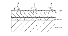
図1(c)のように、AlGaN層14上に電子走行層としてGaN層16をMOCVD法を用い形成する。GaN層16の膜厚は1000nmである。GaN層16上に電子供給層としてAlGaN層18を形成する。AlGaN層18の膜厚は20nmであり、Al組成比は0.2である。AlGaN層18上にキャップ層としてGaN層20を形成する。GaN層20の膜厚は2nmであり、n型である。各層の成長面は(0001)面である。以上により、HEMT用の半導体基板が完成する。
As shown in FIG. 1C, a
AlN層12の膜質は、AlN層12を成長する際の成長温度、成長レート等を制御することで制御することができる。そこで、AlN層12の成長条件を変え、図1(a)の状態でX線回折によるAlNの(002)面のロッキングカーブの半値幅を測定した。同じ条件でAlN層12を成長したウエハを用い、図1(c)の半導体基板を作成し、ウエハの反り量を測定した。図2はウエハの反り量を示すウエハの図である。図2のように、エピタキシャル層を上にし、ウエハ30の端を平面32に接触させた状態で、最も下に凸となっている箇所34と平面32との距離を反り量SORIとした。図2のように、下に凸となっている場合の反り量をプラス、上に凸になっている場合の反り量をマイナスとした。
The film quality of the
図3は、AlN(002)面のロッキングカーブの半値幅に対する反り量SORIを示した図である。図3のように、ロッキングカーブの半値幅が小さくなると反り量SORIが小さくなる。ロッキングカーブの半値幅はAlN層12の結晶性を表している。ロッキングカーブの半値幅が大きい場合、AlN層12のグレインが小さく各グレインの結晶方位のばらつきが大きいことを示している。一方、ロッキングカーブの半値幅が小さい場合、AlN層12のグレインが大きく単結晶により近い状態である。
FIG. 3 is a diagram showing the warping amount SORI with respect to the half width of the rocking curve of the AlN (002) surface. As shown in FIG. 3, when the half-value width of the rocking curve is reduced, the warpage amount SORI is reduced. The full width at half maximum of the rocking curve represents the crystallinity of the
特許文献1に記載されているように、AlGaN層14により、反り量が低減するのは以下のように考えられている。すなわち、各層の成長温度は1000℃前後のため、線熱膨張係数の差に起因して反りが発生する。GaN層16の線熱膨張係数はSiやAlNに比べ大きいため、GaN層16だけではウエハは、下に凸となるように反ってしまう。つまりGaN層16が伸張応力を発生する。特に、良好な半導体装置を作製するためには、AlGaN層14上のGaNを含む層(例えばGaN層16)の膜厚は0.8μm以上となる。このため、ウエハの反り量は非常に大きくなる。そこで、AlN層12上にAlN層12よりa軸長の長いAlGaN層14を設けることにより、格子定数の差に起因し上に凸となるような応力が発生する。つまり、AlGaN層14内にAlN層12により圧縮応力が生じる。このように、AlGaN層14に起因した応力でGaN層に起因した応力を補償することにより、反り量を低減させることができると考えられる。
As described in Patent Document 1, it is considered that the amount of warpage is reduced by the
しかしながら、図3の結果は、AlN層12の結晶性が悪い場合、AlGaN層14に圧縮応力が発生せず、ウエハ全体の反りが大きくなってしまっていると考えられる。AlN(002)面のロッキングカーブの半値幅が異なるウエハを形成したところ、ロッキングカーブの半値幅が3000秒程度の場合、AlGaN層14には圧縮応力がほとんど発生しない。一方、AlN(002)面のロッキングカーブの半値幅が1500秒以下の場合、AlGaN層14に十分な圧縮応力が発生する。ロッキングカーブの半値幅は、1300秒以下であることがより好ましく、1200秒以下であることがより好ましい。
However, the results of FIG. 3 are considered that when the crystallinity of the
さらに、半導体基板の反り量は、半導体基板の大きさを4インチとした場合、±50μm以下(曲率半径が±25m以上)であることが好ましい。反り量が±50μmを越えると、半導体装置のウエハプロセス工程において実用的でなくなる。また、半導体基板にクラックが発生しやすくなる。反り量は±40μm以下、曲率半径は±20m以上がより好ましい。さらに、反り量は±30μm以下、曲率半径は±15m以上がより好ましい。 Furthermore, the warpage amount of the semiconductor substrate is preferably ± 50 μm or less (the radius of curvature is ± 25 m or more) when the size of the semiconductor substrate is 4 inches. If the amount of warpage exceeds ± 50 μm, it becomes impractical in the wafer process step of the semiconductor device. In addition, cracks are likely to occur in the semiconductor substrate. More preferably, the amount of warpage is ± 40 μm or less and the radius of curvature is ± 20 m or more. Further, it is more preferable that the warpage amount is ± 30 μm or less and the curvature radius is ± 15 m or more.
AlN層12上に形成されたGaN系半導体層の例としてAlGaN層14を例に説明したが、GaN系半導体層は、AlN層12から圧縮応力を受ける層であればよい。すなわち、GaN系半導体層は、AlN層12に伸張応力を発生させる層であればよい。なお、GaN系半導体層は、GaNを含む層であり、例えばGaN層、InGaN層、AlGaN層、InAlGaN層、またはこれらの積層である。
Although the
図4は、GaN系半導体層として、AlGaN層14上にGaN層16を設けた構造において、AlGaN層14のAl組成比に対するa軸長の関係を示す図である。図4において、応力を受けていないAlNのa軸長は0.3112nmであり、応力を受けていないGaNのa軸長は0.3189nmである。よって、応力を受けていないAlGaN層のa軸長は、図4のA=−0.0077x+0.3189となる。よって、AlGaN層4が圧縮応力を受けているため、AlGaN層14をAlxGa1−xN層とし、AlGaN14層のa軸長をA nmとしたとき、
A<0.0077x+0.3189
となる。
FIG. 4 is a diagram showing the relationship of the a-axis length with respect to the Al composition ratio of the
A <0.0077x + 0.3189
It becomes.
AlN層12の結晶性が得られるためには、AlN層12の膜厚は100nm以上であることが好ましい。AlN層12の膜厚は150nm以上がより好ましい。また、AlN層12は、クラック等を抑制するため400nm以下であることが好ましい。AlN層12に圧縮応力を印加するためには、AlGaN層14のAl組成比、すなわちAlxGa1−xNのxは0.3以上0.6以上が好ましい。xは0.35以上0.55以下がより好ましい。
In order to obtain the crystallinity of the
実施例2は、実施例1の半導体基板を用い半導体装置を形成する例である。図5は、実施例2に係る半導体装置の断面図である。図4のように、図1(c)の半導体基板のGaN層20上に、例えば蒸着法を用いて、ソース電極24、ドレイン電極26及びゲート電極28を形成する。ソース電極24及びドレイン電極26は、GaN層20に近い方から例えばTi/Auを積層させたオーミック電極である。ゲート電極28は、GaN層20に近い方から例えばNi/Auを積層させてなる。以上により、実施例2に係る半導体装置が完成する。
The second embodiment is an example in which a semiconductor device is formed using the semiconductor substrate of the first embodiment. FIG. 5 is a cross-sectional view of the semiconductor device according to the second embodiment. As shown in FIG. 4, the
実施例1および実施例2は、HEMTを例に説明したが、HEMT以外のトランジスタや、例えばレーザダイオードやフォトダイオードのような光半導体装置でもよい。 In the first and second embodiments, the HEMT has been described as an example. However, a transistor other than the HEMT, or an optical semiconductor device such as a laser diode or a photodiode may be used.
以上、本発明の実施例について詳述したが、本発明はかかる特定の実施例に限定されるものではなく、特許請求の範囲に記載された本発明の要旨の範囲内において、種々の変形・変更が可能である。 Although the embodiments of the present invention have been described in detail above, the present invention is not limited to such specific embodiments, and various modifications and changes can be made within the scope of the gist of the present invention described in the claims. It can be changed.
Si基板 10
AlN層 12
AlGaN層 14
GaN層 16
AlGaN層 18
GaN層 20
Claims (13)
前記AlN層上に形成されたGaN系半導体層と、
を具備することを特徴とする半導体基板。 An AlN layer having a (002) plane rocking curve half-width of 1500 seconds or less formed by X-ray diffraction in contact with a Si substrate;
A GaN-based semiconductor layer formed on the AlN layer;
A semiconductor substrate comprising:
A<0.0077x+0.3189
であることを特徴とする請求項1から3いずれか一項記載の半導体基板。 The GaN-based semiconductor layer is composed includes GaN layer formed on Al x Ga 1-x N layer and said Al x Ga 1-x N layer, a-axis length of the Al x Ga 1-x N layer When the a-axis length is A nm,
A <0.0077x + 0.3189
The semiconductor substrate according to claim 1, wherein the semiconductor substrate is a semiconductor substrate.
前記AlN層上に形成されたGaN系半導体層と、
を具備することを特徴とする半導体装置。 An AlN layer having a (002) plane rocking curve half-width of 1500 seconds or less formed by X-ray diffraction in contact with a Si substrate;
A GaN-based semiconductor layer formed on the AlN layer;
A semiconductor device comprising:
A<0.0077x+0.3189
であることを特徴とする請求項8または9のいずれか一項記載の半導体装置。 The GaN-based semiconductor layer is composed includes GaN layer formed on Al x Ga 1-x N layer and said Al x Ga 1-x N layer, a-axis length of the Al x Ga 1-x N layer When the a-axis length is A nm,
A <0.0077x + 0.3189
The semiconductor device according to claim 8, wherein the semiconductor device is a semiconductor device.
Priority Applications (1)
| Application Number | Priority Date | Filing Date | Title |
|---|---|---|---|
| JP2016007363A JP2016154221A (en) | 2016-01-18 | 2016-01-18 | Semiconductor substrate and semiconductor device |
Applications Claiming Priority (1)
| Application Number | Priority Date | Filing Date | Title |
|---|---|---|---|
| JP2016007363A JP2016154221A (en) | 2016-01-18 | 2016-01-18 | Semiconductor substrate and semiconductor device |
Related Parent Applications (1)
| Application Number | Title | Priority Date | Filing Date |
|---|---|---|---|
| JP2010150058A Division JP2012015303A (en) | 2010-06-30 | 2010-06-30 | Semiconductor substrate and semiconductor device |
Publications (1)
| Publication Number | Publication Date |
|---|---|
| JP2016154221A true JP2016154221A (en) | 2016-08-25 |
Family
ID=56761313
Family Applications (1)
| Application Number | Title | Priority Date | Filing Date |
|---|---|---|---|
| JP2016007363A Pending JP2016154221A (en) | 2016-01-18 | 2016-01-18 | Semiconductor substrate and semiconductor device |
Country Status (1)
| Country | Link |
|---|---|
| JP (1) | JP2016154221A (en) |
Cited By (3)
| Publication number | Priority date | Publication date | Assignee | Title |
|---|---|---|---|---|
| JP2018093112A (en) * | 2016-12-06 | 2018-06-14 | 株式会社サイオクス | Method for manufacturing nitride semiconductor template, nitride semiconductor template, and nitride semiconductor device |
| WO2019123763A1 (en) * | 2017-12-19 | 2019-06-27 | 株式会社Sumco | Method for producing group iii nitride semiconductor substrate |
| WO2021200836A1 (en) * | 2020-03-30 | 2021-10-07 | 東ソー株式会社 | Laminated film, structure including laminated film, semiconductor element, electronic device, and method for producing laminated film |
-
2016
- 2016-01-18 JP JP2016007363A patent/JP2016154221A/en active Pending
Cited By (5)
| Publication number | Priority date | Publication date | Assignee | Title |
|---|---|---|---|---|
| JP2018093112A (en) * | 2016-12-06 | 2018-06-14 | 株式会社サイオクス | Method for manufacturing nitride semiconductor template, nitride semiconductor template, and nitride semiconductor device |
| US11574809B2 (en) | 2016-12-06 | 2023-02-07 | Sumitomo Chemical Company, Limited | Nitride semiconductor template and nitride semiconductor device |
| WO2019123763A1 (en) * | 2017-12-19 | 2019-06-27 | 株式会社Sumco | Method for producing group iii nitride semiconductor substrate |
| JPWO2019123763A1 (en) * | 2017-12-19 | 2020-12-17 | 株式会社Sumco | Method for manufacturing group III nitride semiconductor substrate |
| WO2021200836A1 (en) * | 2020-03-30 | 2021-10-07 | 東ソー株式会社 | Laminated film, structure including laminated film, semiconductor element, electronic device, and method for producing laminated film |
Similar Documents
| Publication | Publication Date | Title |
|---|---|---|
| JP5552923B2 (en) | Semiconductor device and manufacturing method thereof | |
| JP5383974B2 (en) | Semiconductor substrate and semiconductor device | |
| JP6318474B2 (en) | Manufacturing method of semiconductor device | |
| US8546813B2 (en) | Semiconductor substrate and semiconductor device | |
| JP5112370B2 (en) | Manufacturing method of semiconductor device | |
| JP5668339B2 (en) | Manufacturing method of semiconductor device | |
| US8823055B2 (en) | REO/ALO/A1N template for III-N material growth on silicon | |
| JP2009231561A (en) | Nitride semiconductor crystal thin film and its manufacturing method, and semiconductor device and method of manufacturing the same | |
| US7462505B2 (en) | Growth process of a crystalline gallium nitride based compound and semiconductor device including gallium nitride based compound | |
| JP2007112633A (en) | Nitride semiconductor wafer and nitride semiconductor element | |
| WO2014068838A1 (en) | Epitaxial wafer and method for manufacturing same | |
| US20150084163A1 (en) | Epitaxial substrate, semiconductor device, and method for manufacturing semiconductor device | |
| JP2016171196A (en) | Semiconductor device manufacturing method | |
| US20100123139A1 (en) | Semiconductor wafer, semiconductor device, semiconductor wafer manufacturing method and semiconductor device manufacturing method | |
| JP2014022685A (en) | Semiconductor laminate structure and semiconductor element using the same | |
| JP3753068B2 (en) | Method for manufacturing epitaxial wafer for field effect transistor | |
| US20120168771A1 (en) | Semiconductor element, hemt element, and method of manufacturing semiconductor element | |
| JP2016154221A (en) | Semiconductor substrate and semiconductor device | |
| US8823025B1 (en) | III-N material grown on AIO/AIN buffer on Si substrate | |
| JP5817283B2 (en) | Manufacturing method of semiconductor device | |
| US8623747B1 (en) | Silicon, aluminum oxide, aluminum nitride template for optoelectronic and power devices | |
| KR102273305B1 (en) | Gallium nitride semiconductor structure on diamond substrate with improved reliability and process for fabricating thereof | |
| US9437725B2 (en) | Semiconductor device and semiconductor substrate | |
| JP5776344B2 (en) | Semiconductor device | |
| US9355841B2 (en) | Manufacturing method of high electron mobility transistor |