JP2016141012A - Printer and control circuit - Google Patents
Printer and control circuit Download PDFInfo
- Publication number
- JP2016141012A JP2016141012A JP2015017470A JP2015017470A JP2016141012A JP 2016141012 A JP2016141012 A JP 2016141012A JP 2015017470 A JP2015017470 A JP 2015017470A JP 2015017470 A JP2015017470 A JP 2015017470A JP 2016141012 A JP2016141012 A JP 2016141012A
- Authority
- JP
- Japan
- Prior art keywords
- drive
- circuit
- voltage
- control circuit
- peripheral device
- Prior art date
- Legal status (The legal status is an assumption and is not a legal conclusion. Google has not performed a legal analysis and makes no representation as to the accuracy of the status listed.)
- Granted
Links
Images
Classifications
-
- G—PHYSICS
- G06—COMPUTING OR CALCULATING; COUNTING
- G06F—ELECTRIC DIGITAL DATA PROCESSING
- G06F1/00—Details not covered by groups G06F3/00 - G06F13/00 and G06F21/00
- G06F1/26—Power supply means, e.g. regulation thereof
- G06F1/266—Arrangements to supply power to external peripherals either directly from the computer or under computer control, e.g. supply of power through the communication port, computer controlled power-strips
-
- B—PERFORMING OPERATIONS; TRANSPORTING
- B41—PRINTING; LINING MACHINES; TYPEWRITERS; STAMPS
- B41J—TYPEWRITERS; SELECTIVE PRINTING MECHANISMS, i.e. MECHANISMS PRINTING OTHERWISE THAN FROM A FORME; CORRECTION OF TYPOGRAPHICAL ERRORS
- B41J29/00—Details of, or accessories for, typewriters or selective printing mechanisms not otherwise provided for
- B41J29/38—Drives, motors, controls or automatic cut-off devices for the entire printing mechanism
- B41J29/393—Devices for controlling or analysing the entire machine ; Controlling or analysing mechanical parameters involving printing of test patterns
-
- B—PERFORMING OPERATIONS; TRANSPORTING
- B41—PRINTING; LINING MACHINES; TYPEWRITERS; STAMPS
- B41J—TYPEWRITERS; SELECTIVE PRINTING MECHANISMS, i.e. MECHANISMS PRINTING OTHERWISE THAN FROM A FORME; CORRECTION OF TYPOGRAPHICAL ERRORS
- B41J29/00—Details of, or accessories for, typewriters or selective printing mechanisms not otherwise provided for
- B41J29/38—Drives, motors, controls or automatic cut-off devices for the entire printing mechanism
-
- G—PHYSICS
- G06—COMPUTING OR CALCULATING; COUNTING
- G06F—ELECTRIC DIGITAL DATA PROCESSING
- G06F1/00—Details not covered by groups G06F3/00 - G06F13/00 and G06F21/00
- G06F1/26—Power supply means, e.g. regulation thereof
- G06F1/32—Means for saving power
- G06F1/3203—Power management, i.e. event-based initiation of a power-saving mode
- G06F1/3234—Power saving characterised by the action undertaken
- G06F1/325—Power saving in peripheral device
- G06F1/3284—Power saving in printer
-
- G—PHYSICS
- G07—CHECKING-DEVICES
- G07G—REGISTERING THE RECEIPT OF CASH, VALUABLES, OR TOKENS
- G07G5/00—Receipt-giving machines
-
- G—PHYSICS
- G06—COMPUTING OR CALCULATING; COUNTING
- G06F—ELECTRIC DIGITAL DATA PROCESSING
- G06F1/00—Details not covered by groups G06F3/00 - G06F13/00 and G06F21/00
- G06F1/26—Power supply means, e.g. regulation thereof
-
- G—PHYSICS
- G06—COMPUTING OR CALCULATING; COUNTING
- G06Q—INFORMATION AND COMMUNICATION TECHNOLOGY [ICT] SPECIALLY ADAPTED FOR ADMINISTRATIVE, COMMERCIAL, FINANCIAL, MANAGERIAL OR SUPERVISORY PURPOSES; SYSTEMS OR METHODS SPECIALLY ADAPTED FOR ADMINISTRATIVE, COMMERCIAL, FINANCIAL, MANAGERIAL OR SUPERVISORY PURPOSES, NOT OTHERWISE PROVIDED FOR
- G06Q20/00—Payment architectures, schemes or protocols
- G06Q20/08—Payment architectures
- G06Q20/20—Point-of-sale [POS] network systems
-
- G—PHYSICS
- G07—CHECKING-DEVICES
- G07G—REGISTERING THE RECEIPT OF CASH, VALUABLES, OR TOKENS
- G07G1/00—Cash registers
- G07G1/12—Cash registers electronically operated
Landscapes
- Engineering & Computer Science (AREA)
- Theoretical Computer Science (AREA)
- General Engineering & Computer Science (AREA)
- Physics & Mathematics (AREA)
- General Physics & Mathematics (AREA)
- Computer Hardware Design (AREA)
- Power Sources (AREA)
- Accessory Devices And Overall Control Thereof (AREA)
- Cash Registers Or Receiving Machines (AREA)
Abstract
Description
本発明は、プリンタ及び制御回路に関する。 The present invention relates to a printer and a control circuit.
店舗等において売上を入力し、入出金やレシートの発行を行う装置として、POS(Point Of Sale)を管理できるPOSシステムが知られている。POSシステムは、POS端末、プリンタ、およびキャッシュドロワなどの周辺機器で構成されている。 2. Description of the Related Art A POS system capable of managing POS (Point Of Sale) is known as an apparatus for inputting sales at a store or the like and issuing deposits / withdrawals and receipts. The POS system includes peripheral devices such as a POS terminal, a printer, and a cash drawer.
従来より、キャッシュドロワと接続しているプリンタが知られており、例えば特許文献1に開示されている。
一般的なPOSシステムにおいては、プリンタ用の電源をキャッシュドロワ用の電源にも供給しているが、プリンタとキャッシュドロワの駆動電圧は必ずしも一致せず、この場合、キャッシュドロワ用の電源をプリンタの内部で生成する必要がある。
Conventionally, a printer connected to a cash drawer is known, and for example, disclosed in Patent Document 1.
In a general POS system, the printer power supply is also supplied to the cash drawer power supply, but the drive voltage of the printer and the cash drawer do not necessarily match. In this case, the power supply for the cash drawer is not connected to the printer. Must be generated internally.
しかし、キャッシュドロワの駆動時間はPOSシステムが稼動している時間において、極めて短時間であり、キャッシュドロワ用の電源を常時プリンタ内部で生成していることは非常に電源効率を下げることになる。 However, the cash drawer driving time is extremely short during the time when the POS system is operating, and the fact that the power for the cash drawer is always generated inside the printer greatly reduces the power efficiency.
そこで、プリンタは、電源生成信号が入力されると電源をキャッシュドロワに供給する電源生成回路と、駆動信号が入力されるとキャッシュドロワを駆動する駆動回路と、電源生成信号および駆動信号を出力するプリンタコントローラを備える構成にすることが考えられる。この構成により、プリンタの電源効率を上げるため、キャッシュドロワを駆動する時だけ、キャッシュドロワ用の電源を生成する手法が考えられる。しかし、従来のプリンタでは、電源生成と同時にキャッシュドロワを駆動しようとすると、電源生成回路が立ち上がっておらず、出力として十分な電力が得られないうちに、予め設定されたキャッシュドロワの駆動期間が終了し、キャッシュドロワを駆動できないといった問題が生じてしまうおそれがある。 Accordingly, the printer outputs a power generation signal and a drive signal, a power generation circuit that supplies power to the cash drawer when a power generation signal is input, a drive circuit that drives the cash drawer when a drive signal is input. It can be considered to have a configuration including a printer controller. In order to increase the power efficiency of the printer with this configuration, a method of generating a power source for the cash drawer only when driving the cash drawer can be considered. However, in the conventional printer, when the cash drawer is driven simultaneously with the generation of the power, the power generation circuit is not started up, and a sufficient cash drawer driving period is obtained before sufficient power is obtained as an output. This may end up and cause a problem that the cash drawer cannot be driven.
また、キャッシュドロワを今まで使用していたものと異なる機種のキャッシュドロワに置き換えた場合、キャッシュドロワに供給する駆動電圧が異なることがある。これに対応するため、プリンタコントローラから電圧指定信号を電源生成回路に対して出力し、必要な駆動電圧を生成する手法が考えられる。しかし、駆動電圧の違いにより電源生成回路の立ち上がり時間が異なるため、上述のような、予め設定されたキャッシュドロワの駆動期間が終了し、キャッシュドロワを駆動できないといった問題が生じてしまうおそれがある。
なお、異なる駆動電圧のキャッシュドロワを駆動するため、プリンタ内部の駆動回路に定電流回路を設けることが特許文献1に示されている。しかしながら、この手法では、電流が制限されるので、キャッシュドロワに必要な電力が得られず、必要な駆動電圧でキャッシュドロワを駆動できないという問題が生じる。
Further, when the cash drawer is replaced with a cash drawer of a different model from that used so far, the drive voltage supplied to the cash drawer may be different. In order to cope with this, a method of generating a necessary drive voltage by outputting a voltage designation signal from the printer controller to the power generation circuit can be considered. However, since the rise time of the power generation circuit varies depending on the drive voltage, there is a possibility that the preset cash drawer drive period ends as described above and the cash drawer cannot be driven.
Note that Patent Document 1 discloses that a constant current circuit is provided in a drive circuit inside a printer in order to drive cash drawers having different drive voltages. However, in this method, since the current is limited, the power required for the cash drawer cannot be obtained, and there is a problem that the cash drawer cannot be driven with a necessary drive voltage.
そこで、本発明は、上記のような問題点を解決するためになされたものであり、電源効率が高いプリンタを提供することにある。 Accordingly, the present invention has been made to solve the above-described problems and provides a printer with high power supply efficiency.
上記の課題を解決するために、本発明のプリンタは、周辺機器と接続しているプリンタであって、前記周辺機器に対して前記周辺機器の動作に必要な予め設定された駆動電圧を供給する電源生成回路と、駆動信号が入力されると、前記周辺機器を前記駆動電圧で動作させる駆動回路と、前記駆動回路が動作する予め設定された駆動期間の間だけ、前記駆動回路に対して前記駆動信号を出力して、前記駆動回路を動作させる制御回路と、を備えることを特徴とする。 In order to solve the above problems, a printer of the present invention is a printer connected to a peripheral device, and supplies a preset drive voltage necessary for the operation of the peripheral device to the peripheral device. When a drive signal is input to the power supply generation circuit, the drive circuit that operates the peripheral device with the drive voltage, and the drive circuit with respect to the drive circuit only during a preset drive period in which the drive circuit operates. And a control circuit that outputs a drive signal and operates the drive circuit.
また、本発明のプリンタは、前記制御回路は、外部から前記周辺機器の動作を開始する開始指示が入力されると、前記電源生成回路が生成する前記駆動電圧を決定し、前記駆動電圧を表す電圧指定信号を前記電源生成回路に対して出力し、前記周辺機器に供給する供給電圧が初期値から前記駆動電圧になるまでの予め設定された立ち上り時間を決定し、電源生成信号を前記電源生成回路に対して出力し、前記電源生成回路に対して前記周辺機器に前記供給電圧を供給することを開始させ、前記供給電圧が前記駆動電圧になるまでの時間を計測し、計測時間が前記立ち上り時間になった場合である前記駆動期間の開始時期において、前記駆動回路に対して前記駆動信号を出力し、前記駆動期間の終了時期において、前記電圧指定信号、前記電源生成信号および前記駆動信号の出力を停止する、ことを特徴とする。 In the printer according to the aspect of the invention, the control circuit may determine the drive voltage generated by the power generation circuit when the start instruction for starting the operation of the peripheral device is input from the outside, and represents the drive voltage. A voltage designation signal is output to the power generation circuit, a preset rise time from when the supply voltage supplied to the peripheral device becomes the drive voltage from an initial value is determined, and the power generation signal is generated by the power generation Output to the circuit, start supplying the supply voltage to the peripheral device to the power generation circuit, measure the time until the supply voltage becomes the drive voltage, The drive signal is output to the drive circuit at the start time of the drive period, which is a time, and at the end time of the drive period, the voltage designation signal, the power supply It stops outputting the formed signal and the drive signal, characterized in that.
また、本発明のプリンタは、前記制御回路に接続され、外部のホスト装置からのデータ入力を受信する通信回路を備え、前記駆動期間、前記開始指示、前記制御回路が決定する前記駆動電圧、前記立ち上り時間は、前記通信回路を介して前記制御回路に入力される、ことを特徴とする。 The printer of the present invention includes a communication circuit connected to the control circuit and receiving data input from an external host device, the drive period, the start instruction, the drive voltage determined by the control circuit, The rise time is input to the control circuit via the communication circuit.
また、本発明のプリンタは、前記制御回路に接続され、外部のホスト装置からのデータ入力を受信する通信回路および不揮発性メモリを備え、前記駆動期間および前記開始指示は、前記通信回路を介して前記制御回路に入力され、前記制御回路が決定する前記駆動電圧、前記立ち上り時間は、前記不揮発性メモリに予め記憶されている、ことを特徴とする。 The printer of the present invention includes a communication circuit and a nonvolatile memory that are connected to the control circuit and receive data input from an external host device, and the drive period and the start instruction are transmitted via the communication circuit. The drive voltage and the rise time that are input to the control circuit and determined by the control circuit are stored in advance in the nonvolatile memory.
また、本発明のプリンタは、前記制御回路に接続され、外部のホスト装置からのデータ入力を受信する通信回路および不揮発性メモリを備え、前記開始指示は、前記通信回路を介して前記制御回路に入力され、前記制御回路が決定する前記駆動電圧、前記立ち上り時間および前記駆動期間は、前記不揮発性メモリに予め記憶されている、ことを特徴とする。 The printer of the present invention includes a communication circuit and a nonvolatile memory that are connected to the control circuit and receive data input from an external host device, and the start instruction is sent to the control circuit via the communication circuit. The drive voltage, the rise time, and the drive period that are input and determined by the control circuit are stored in advance in the nonvolatile memory.
また、本発明のプリンタは、前記制御回路に接続され、外部のホスト装置からのデータ入力を受信する通信回路および不揮発性メモリを備え、前記駆動期間、前記開始指示および前記周辺機器の機種名は、前記通信回路を介して前記制御回路に入力され、前記制御回路が決定する前記駆動電圧、前記立ち上り時間は、前記不揮発性メモリに前記周辺機器の機種名に対応して複数個予め記憶されている、ことを特徴とする。 The printer of the present invention includes a communication circuit and a nonvolatile memory that are connected to the control circuit and receive data input from an external host device. The drive period, the start instruction, and the model name of the peripheral device are A plurality of the drive voltage and the rise time input to the control circuit via the communication circuit and determined by the control circuit are stored in advance in the nonvolatile memory corresponding to the model name of the peripheral device. It is characterized by that.
また、本発明のプリンタは、前記制御回路に接続され、外部のホスト装置からのデータ入力を受信する通信回路および不揮発性メモリを備え、前記開始指示および前記周辺機器の機種名は、前記通信回路を介して前記制御回路に入力され、前記制御回路が決定する前記駆動電圧、前記立ち上り時間および前記駆動期間は、前記不揮発性メモリに前記周辺機器の機種名に対応して複数個予め記憶されている、ことを特徴とする。 In addition, the printer of the present invention includes a communication circuit and a nonvolatile memory that are connected to the control circuit and receive data input from an external host device, and the start instruction and the model name of the peripheral device are the communication circuit The drive voltage, the rise time, and the drive period determined by the control circuit are stored in advance in the nonvolatile memory corresponding to the model name of the peripheral device. It is characterized by that.
本発明の制御回路は、周辺機器に対して前記周辺機器の動作に必要な駆動電圧を供給する電源生成回路と、駆動信号が入力されると、前記周辺機器を前記駆動電圧で動作させる駆動回路と、を備えた、前記周辺機器と接続しているプリンタの制御回路であって、前記駆動回路が動作する駆動期間の間だけ、前記駆動回路に対して前記駆動信号を出力して、前記駆動回路を動作させる、ことを特徴とする。 The control circuit of the present invention includes a power generation circuit that supplies a drive voltage necessary for the operation of the peripheral device to the peripheral device, and a drive circuit that operates the peripheral device at the drive voltage when a drive signal is input. A control circuit for a printer connected to the peripheral device, wherein the drive signal is output to the drive circuit only during a drive period during which the drive circuit operates, and the drive The circuit is operated.
本発明によれば、電源生成回路は、周辺機器(例えばキャッシュドロワ)に対して周辺機器の動作に必要な予め設定された駆動電圧を供給する。また、駆動回路は、駆動信号が入力されると、周辺機器を駆動電圧で動作させる。そして、制御回路は、駆動回路が動作する予め設定された駆動期間の間だけ、駆動回路に対して駆動信号を出力して、駆動回路を動作させる制御を行う。これにより、電源生成回路は、予め設定された周辺機器の駆動期間において駆動電圧を周辺機器に対して供給するので、周辺機器を駆動できないといった問題が生じるおそれはなくなる。また、本発明によれば、周辺機器を駆動するときにだけ周辺機器を駆動させるための電源を生成して供給する構成になっているので、電源効率が高いプリンタを提供することができる。 According to the present invention, the power supply generation circuit supplies a preset driving voltage necessary for the operation of the peripheral device to the peripheral device (for example, cash drawer). The drive circuit operates the peripheral device with the drive voltage when the drive signal is input. Then, the control circuit outputs a drive signal to the drive circuit only during a preset drive period during which the drive circuit operates, and performs control to operate the drive circuit. As a result, the power supply generation circuit supplies the drive voltage to the peripheral device during a preset drive period of the peripheral device, so that there is no possibility of causing a problem that the peripheral device cannot be driven. In addition, according to the present invention, since the power for driving the peripheral device is generated and supplied only when the peripheral device is driven, a printer with high power efficiency can be provided.
以下、本発明の実施形態について図面を参照しながら説明する。 Hereinafter, embodiments of the present invention will be described with reference to the drawings.
[第1の実施形態]
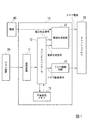
図1は、本実施形態におけるプリンタの構成を示すブロック図である。
図1に示すように、プリンタ10は、通信回路11、プリンタコントローラ12(制御回路)、電源生成回路13、ドロワ駆動回路14、および不揮発性メモリ15を備える。
[First Embodiment]
FIG. 1 is a block diagram illustrating a configuration of a printer according to the present embodiment.
As shown in FIG. 1, the
通信回路11は、プリンタ10の外部にあるホスト装置20(POS端末)に接続される。ホスト装置20は、商品名や価格などを入力するための入力キー、POSシステムの各種設定を行うための操作キーを有している。また、ホスト装置20は、プリンタ10に対してレシートの発行、キャッシュドロワ30(周辺機器)の開閉を指示するための制御命令を、プリンタ10の通信回路11に送信する。
通信回路11は、ホスト装置20からのデータ入力を受信し、データ入力に含まれる制御命令をプリンタコントローラ12に対して送信する。
The
The
プリンタコントローラ12は、通信回路11が、ホスト装置20からのデータ入力を受信し、データ入力に含まれる制御命令に応じてプリンタ10の各部を制御する。例えば、プリンタコントローラ12は、図1において不図示の印刷部に印刷データの内容をレシートなどの印刷用紙に印刷させる。また、プリンタコントローラ12は、通信回路11が、ホスト装置20から受信したキャッシュドロワ30のドロワトレイを開閉すべき旨の制御命令(開始指示)に応じて、電源生成回路13およびドロワ駆動回路14に対して、キャッシュドロワ30を駆動するための電圧を供給すべき旨の制御命令(電圧指定信号、電源生成信号およびドロワ駆動信号)を出力する。
In the
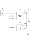
ここで、図2を用いて、電源生成回路13、キャッシュドロワ30、ドロワ駆動回路14の接続関係について説明する。図2は、電源生成回路13、キャッシュドロワ30、ドロワ駆動回路14の接続関係を示す図である。
電源生成回路13の入力端子には、電源40からの電源40が供給する電圧、プリンタコントローラ12からの電圧指定信号、電源生成信号が入力される。また、電源生成回路13は、出力端子が接続ケーブル30Uを介してキャッシュドロワ30を構成するソレノイドコイル30Sの一端に接続される。電源生成回路13は、電源40が供給する電圧を変換し、変換後の電圧であるドロワ電源(供給電圧)を出力端子から出力し、接続ケーブル30Uを介して、ソレノイドコイル30Sの一端に供給する。
Here, the connection relationship of the
A voltage supplied by the
ドロワ駆動回路14を構成するトランジスタ14Bは、例えばバイポーラトランジスタである。トランジスタ14Bのコレクタ端子(出力端子)は、接続ケーブル30Dを介してキャッシュドロワ30を構成するソレノイドコイル30Sの他端に接続される。トランジスタ14Bのベース端子(入力端子)は、プリンタコントローラ12からのドロワ駆動信号(駆動信号)が入力される。また、トランジスタ14Bのエミッタ端子は、接地される。
The
ソレノイドコイル30Sは、キャッシュドロワ30のロック機構を構成する素子である。ソレノイドコイル30Sは、両端子間に動作に必要な予め設定された駆動電圧が加わると、ロック機構をロック解除状態にし、逆に両端子間に動作に必要な予め設定された駆動電圧が加わらないと、ロック機構をロック解除状態にすることができない。
The
図1に戻って、電源生成回路13は、電源40に接続されている。電源40は、プリンタ10の主電源である。
電源生成回路13は、電源40が供給する電圧を変換し、変換後の電圧であるドロワ電源を出力端子から出力し、ソレノイドコイル30Sの一端に供給する。このドロワ電源の目標値が、キャッシュドロワ30の動作に必要な予め設定された駆動電圧(以下、駆動電圧V1とする)である。
電源生成回路13は、駆動電圧V1を表す電圧指定信号がプリンタコントローラ12から入力されると、ドロワ電源の目標値を駆動電圧V1に設定する。また、電源生成回路13は、駆動電圧V1の設定後、電源生成信号がプリンタコントローラ12から入力されると、ドロワ電源の目標値が駆動電圧V1となるように、出力端子からのドロワ電源の出力を開始する。
Returning to FIG. 1, the power
The power
When a voltage designation signal representing the drive voltage V1 is input from the
ドロワ駆動回路14は、ドロワ駆動信号がプリンタコントローラ12から入力されると、ドロワ駆動信号が入力されている期間、トランジスタ14Bをオン状態にし、ソレノイドコイル30Sを駆動する。このドロワ駆動信号が入力されている期間は、ソレノイドコイル30Sの駆動期間であり、予め設定された駆動期間(以下、駆動期間T0とする)である。
When a drawer drive signal is input from the
不揮発性メモリ15は、本実施形態においては、プリンタコントローラ12が実行する制御方法を記憶する。
In the present embodiment, the
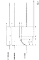
プリンタコントローラ12は、上述の様に、電圧指定信号、電源生成信号、ドロワ駆動信号を出力し、電源生成回路13、ドロワ駆動回路14を制御することにより、キャッシュドロワ30の動作を制御する。しかしながら、従来においては、次に説明するような問題があった。図3は、従来におけるプリンタの操作処理での問題点を説明するための図である。図3において、横軸は時刻を示しており、縦軸は、ドロワ駆動信号、電源生成信号、ドロワ電源のレベル変化を示している。
プリンタコントローラ12は、時刻t1において、電源生成回路13にドロワ電源をキャッシュドロワ30に供給させるために、電源生成信号をLレベルからHレベルに変化させる。
As described above, the
The
また、プリンタコントローラ12は、この時刻t1において、キャッシュドロワ30を駆動するために、ドロワ駆動信号をLレベルからHレベルに変化させる。これにより、ドロワ駆動回路14のトランジスタ14Bはオンし、キャッシュドロワ30のソレノイドコイル30Sの両端にドロワ電源が加わる。
しかし、ドロワ電源が、キャッシュドロワ30の動作に必要な駆動電圧V1に到達するのは時刻t2である。また、ドロワ駆動信号がLレベルに戻る時刻はt4であるから、駆動期間T0のうち(t2−t1)の時間(立ち上り時間T1)は、キャッシュドロワ30の動作に必要な駆動電圧が得られずに、駆動期間T0においてキャッシュドロワ30を駆動できなくなるという問題が発生する。
Further, the
However, it is at time t2 that the drawer power source reaches the drive voltage V1 necessary for the operation of the
また、キャッシュドロワ30を他の機種に置き換える場合、キャッシュドロワ30の動作に必要な駆動電圧が駆動電圧V1から駆動電圧V2へ変わることがある。この場合、ドロワ電源が、キャッシュドロワ30の動作に必要な駆動電圧V2に到達するのは時刻t3である。また、ドロワ駆動信号がLレベルに戻る時刻はt4であるから、駆動期間T0のうち(t3−t1)の時間(立ち上り時間T2)は、キャッシュドロワ30の動作に必要な駆動電圧が得られずに、駆動期間T0においてキャッシュドロワ30を駆動できなくなるという問題が発生する。特に、この場合は駆動電圧V2>駆動電圧V1である場合であることから、置き換えた機種の駆動電圧が大きくなると、立ち上り時間のドロワ電源の駆動期間T0に占める割合が大きくなる(ドロワ電源が駆動電圧にある時間のドロワ電源駆動期間T0に占める割合が小さくなる)。
When the
そこで、上記問題点を解決し、電源効率が高いプリンタを提供するため、プリンタコントローラ12は、以下のように、電圧指定信号、電源生成信号、ドロワ駆動信号を出力して、電源生成回路13、ドロワ駆動回路14を制御することにより、キャッシュドロワ30の動作を制御する。
プリンタコントローラ12は、通信回路11がホスト装置20から受信したキャッシュドロワ30の動作を開始する開始指示に応じて、電源生成回路13が生成する駆動電圧(上記駆動電圧V1、駆動電圧V2などのキャッシュドロワ30の機種に応じた駆動電圧)を決定する。本実施形態において、駆動電圧は、ホスト装置20から与えられる。プリンタコントローラ12は、駆動電圧を表す電圧指定信号を電源生成回路13に対して出力する。電源生成回路13は、駆動電圧を表す電圧指定信号がプリンタコントローラ12から入力されると、ドロワ電源の目標値を駆動電圧に設定する。
In order to solve the above problems and provide a printer with high power efficiency, the
The
また、プリンタコントローラ12は、電源生成回路13がキャッシュドロワ30に供給するドロワ電源が初期値(Lレベル)から駆動電圧になるまでの予め設定された立ち上り時間(上記立ち上り時間T1、立ち上り時間T2などのキャッシュドロワ30の機種に応じた立ち上り時間であり、予め実験などにより求められた時間)を決定する。本実施形態において、立ち上り時間は、ホスト装置20から与えられる。プリンタコントローラ12は、電源生成信号を電源生成回路13に対して出力する。電源生成回路13は、駆動電圧の設定後、電源生成信号がプリンタコントローラ12から入力されると、出力端子からのドロワ電源の出力を開始する。
Further, the
また、プリンタコントローラ12は、ドロワ電源が駆動電圧になるまでの時間を計測し、計測時間が立ち上り時間になった場合である駆動期間T0の開始時期において、ドロワ駆動回路14に対してドロワ駆動信号を出力する。これにより、駆動期間T0において、キャッシュドロワ30は、ドロワ電源の目標値である駆動電圧によって駆動されるので、キャッシュドロワ30を駆動できなくなることはなくなる。
また、プリンタコントローラ12は、駆動期間T0の終了時期において、電圧指定信号、電源生成信号およびドロワ駆動信号の出力を停止する。駆動期間T0の開始時期および駆動期間T0の終了時期で表される期間は駆動期間T0であり、この駆動期間T0はホスト装置20から与えられる。
Further, the
Further, the
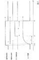
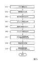
続いて、図4および図5を用いてキャッシュドロワ30の駆動動作について説明する。図4は、本実施形態におけるキャッシュドロワの駆動動作を示すタイミングチャートである。また、図5は、本実施形態におけるキャッシュドロワの駆動動作を示すフローチャートである。図4において、横軸は時刻を示しており、縦軸は、電圧指定信号、ドロワ駆動信号、電源生成信号、ドロワ電源のレベル変化を示している。
なお、本実施形態において、キャッシュドロワ30の動作に必要な予め設定された駆動電圧は駆動電圧V1、ドロワ電源の立ち上り時間は立ち上り時間T1として説明する。
ホスト装置20がドロワ駆動命令をプリンタ10に対して与える(ステップST1)。
プリンタコントローラ12は、駆動電圧を決定する(ステップST2)。
プリンタコントローラ12は、通信回路11がホスト装置20から受信したドロワ駆動命令(キャッシュドロワ30の動作を開始する開始指示)に応じて、電源生成回路13が生成する駆動電圧V1を決定する。本実施形態において、駆動電圧V1は、ホスト装置20から開始指示とともに与えられる。
Subsequently, the driving operation of the
In the present embodiment, the drive voltage V1 set in advance necessary for the operation of the
The
The
The
プリンタコントローラ12は、電圧指定信号を出力する(ステップST3)。プリンタコントローラ12は、図4に示す時刻t1において、駆動電圧V1を表す電圧指定信号を電源生成回路13に対して出力する。電源生成回路13は、駆動電圧V1を表す電圧指定信号がプリンタコントローラ12から入力されると、ドロワ電源の目標値を駆動電圧V1に設定する。
プリンタコントローラ12は、立ち上り時間を決定する(ステップST4)。
プリンタコントローラ12は、電源生成回路13がキャッシュドロワ30に供給するドロワ電源が初期値(Lレベル)から駆動電圧になるまでの予め設定された立ち上り時間T1を決定する。本実施形態において、立ち上り時間T1は、ホスト装置20から開始指示とともに与えられる。
The
The
The
プリンタコントローラ12は、電源生成信号を出力する(ステップST5)。プリンタコントローラ12は、図4に示す時刻t2において、電源生成信号を電源生成回路13に対して出力する。電源生成回路13は、駆動電圧V1の設定後、電源生成信号がプリンタコントローラ12から入力されると、出力端子からのドロワ電源の出力を開始する。
なお、図4において、プリンタコントローラ12が駆動電圧V1を表す電圧指定信号を出力する時刻t1と、プリンタコントローラ12が電源生成信号を出力する時刻t2が異なるが同時であっても構わない。図4は、現在の回路の機能を反映したものであり、電源生成回路13がドロワ電源の目標値を駆動電圧V1に正しく設定した後、出力端子からのドロワ電源の出力を開始することを示しているものにすぎない。
The
In FIG. 4, the time t1 when the
プリンタコントローラ12は、立ち上り時間の計測を行う(ステップST6)。プリンタコントローラ12は、ドロワ電源が駆動電圧V1になるまでの立ち上り時間T1を計測する。
プリンタコントローラ12は、立ち上り時間経過後ドロワ駆動信号を出力する(ステップST7)。プリンタコントローラ12は、図4に示す時刻t3において、すなわち、計測時間が立ち上り時間T1になった場合である駆動期間T0の開始時期において、ドロワ駆動回路14に対してドロワ駆動信号を出力する。これにより、駆動期間T0において、キャッシュドロワ30の動作に必要な予め設定された駆動電圧V1を、キャッシュドロワ30に供給することが可能となる。
The
The
プリンタコントローラ12は、駆動期間の計測を行う(ステップST8)。
プリンタコントローラ12は、駆動期間経過後すべての信号の出力を停止する(ステップST9)。
プリンタコントローラ12は、図4に示す時刻t4において、すなわち、駆動期間T0の終了時期において、電圧指定信号、電源生成信号およびドロワ駆動信号の出力を停止する。
これにより、駆動期間T0において、ドロワ電源のレベルは駆動電圧V1となっており、従来のような立ち上り時間T1が駆動期間T0に占めることをなくすことができる。
The
The
The
Thereby, in the driving period T0, the level of the drawer power supply is the driving voltage V1, and it is possible to prevent the conventional rise time T1 from occupying the driving period T0.
[第2の実施形態]
第2の実施形態において、不揮発性メモリ15は、第1の実施形態と同じく、プリンタコントローラ12が実行する制御方法を記憶する。また、不揮発性メモリ15は、第1の実施形態と相違して、キャッシュドロワ30の動作に必要な予め設定された駆動電圧、ドロワ電源の立ち上り時間を記憶する。
すなわち、不揮発性メモリ15は、キャッシュドロワ30の機種名(MN1、MN2、…、MNN)に対応して、駆動電圧(V1、V2、…VN)、立ち上り時間(T1,T2、…TN)を予め記憶している。駆動電圧、立ち上り時間は、その機種をプリンタ10が駆動する実験を行うことによって得られた実験結果に応じて、不揮発性メモリ15に記憶されている。
なお、不揮発性メモリ15でなく、プリンタコントローラ12が、周辺機器の機種名に対応して、駆動電圧、立ち上り時間を予め記憶する不揮発性メモリを内蔵する構成にしてもよい。
[Second Embodiment]
In the second embodiment, the
That is, the
Note that, instead of the
プリンタコントローラ12は、ホスト装置20から、キャッシュドロワ30の動作を開始する開始指示、駆動期間T0、キャッシュドロワの機種名MNi(i=1〜N)が通信回路11を介して入力される。
プリンタコントローラ12は、キャッシュドロワの機種名MNiに対応した駆動電圧Vi、立ち上り時間Tiを不揮発性メモリ15から読み出し、読み出した値を駆動電圧Vi、立ち上り時間Tiに決定し、電源生成回路13、ドロワ駆動回路14の制御を行う。このときの制御方法は、第1の実施形態において説明した制御方法と同じであるので、以下、第1の実施形態と同様に図4および図5を用いて説明する。なお、本実施形態において、キャッシュドロワの機種名MN1に対応した制御について、キャッシュドロワ30の動作に必要な予め設定された駆動電圧は駆動電圧V1、ドロワ電源の立ち上り時間は立ち上り時間T1として説明する。
The
The
プリンタコントローラ12は、通信回路11がホスト装置20から受信したドロワ駆動命令(キャッシュドロワ30の動作を開始する開始指示)に応じて、キャッシュドロワの機種名MN1に対応した駆動電圧V1を不揮発性メモリ15から読み出し、電源生成回路13が生成する駆動電圧V1を決定する(ステップST1、ST2)。
In response to the drawer drive command (start instruction to start the operation of the cash drawer 30) received by the
プリンタコントローラ12は、図4に示す時刻t1において、駆動電圧V1を表す電圧指定信号を電源生成回路13に対して出力する。電源生成回路13は、駆動電圧V1を表す電圧指定信号がプリンタコントローラ12から入力されると、ドロワ電源の目標値を駆動電圧V1に設定する(ステップST3)。
プリンタコントローラ12は、キャッシュドロワの機種名MN1に対応した立ち上り時間T1を不揮発性メモリ15から読み出し、電源生成回路13がキャッシュドロワ30に供給するドロワ電源が初期値(Lレベル)から駆動電圧になるまでの予め設定された立ち上り時間T1を決定する(ステップST4)。
The
The
プリンタコントローラ12は、図4に示す時刻t2において、電源生成信号を電源生成回路13に対して出力する(ステップST5)。電源生成回路13は、駆動電圧V1の設定後、電源生成信号がプリンタコントローラ12から入力されると、出力端子からのドロワ電源の出力を開始する。
プリンタコントローラ12は、ドロワ電源が駆動電圧V1になるまでの立ち上り時間T1を計測する(ステップST6)。
プリンタコントローラ12は、図4に示す時刻t3において、すなわち、計測時間が立ち上り時間T1になった場合である駆動期間T0の開始時期において、ドロワ駆動回路14に対してドロワ駆動信号を出力する(ステップST7)。これにより、駆動期間T0において、キャッシュドロワ30の動作に必要な予め設定された駆動電圧V1を、キャッシュドロワ30に供給することが可能となる。
The
The
The
プリンタコントローラ12は、駆動期間の計測を行い、駆動期間経過後すべての信号の出力を停止する(ステップST8、ST9)。プリンタコントローラ12は、図4に示す時刻t4において、すなわち、駆動期間T0の終了時期において、電圧指定信号、電源生成信号およびドロワ駆動信号の出力を停止する。
これにより、第1の実施形態と同様に、駆動期間T0において、ドロワ電源のレベルは駆動電圧V0となっており、従来のような立ち上り時間T1が駆動期間T0に占めることをなくすことができる。
The
As a result, as in the first embodiment, the level of the drawer power supply is the drive voltage V0 in the drive period T0, and the conventional rise time T1 can be prevented from occupying the drive period T0.
また、第2の実施形態においては、第1の実施形態とは異なり、駆動電圧Vi、立ち上り時間Tiのプリンタ10の外部からの入力が不要である。従って、例えば第1の実施形態において、ユーザーがキャッシュドロワ30の駆動を開始する際、駆動電圧Vi、立ち上り時間Tiの値を忘れているため、与えることができないといった場合が考えられる。しかし、第2の実施形態においては、こうした場合、機種名MNiを与えることにより、不揮発性メモリ15が記憶している駆動電圧Vi、立ち上り時間Tiを読み出すことにより、キャッシュドロワ30の駆動を正確に開始することができるというメリットがある。なお、キャッシュドロワ30の機種名が同じ名前の場合であっても、駆動電圧が複数個ある場合がある。こうした場合であっても、複数個ある駆動電圧Vi、立ち上り時間Tiの組合せを、例えば改名された機種名に対応して不揮発性メモリ15に記憶しておき、改名された機種名を入力することにより、駆動電圧Vi、立ち上り時間Tiによりキャッシュドロワ30の駆動を正確に開始することができる。
Also, in the second embodiment, unlike the first embodiment, it is not necessary to input the drive voltage Vi and the rise time Ti from the outside of the
以上、第1の実施形態、第2の実施形態でプリンタ10によるキャッシュドロワ30の駆動について説明した。すなわち、両実施形態のプリンタ10は、電源生成回路13が、キャッシュドロワ30に対してキャッシュドロワ30の動作に必要な予め設定された駆動電圧V1を供給する。また、ドロワ駆動回路14は、ドロワ駆動信号が入力されると、キャッシュドロワ30を駆動電圧V1で動作させる。そして、プリンタコントローラ12は、ドロワ駆動回路14が動作する予め設定された駆動期間T0の間だけ、ドロワ駆動回路14に対して駆動信号を出力して、ドロワ駆動回路14を動作させる制御を行う。
The driving of the
これにより、プリンタ10は、電源生成回路13が、予め設定されたキャッシュドロワ30の駆動期間T0において駆動電圧V1をキャッシュドロワ30に対して供給するので、キャッシュドロワ30を駆動できないといった問題が生じるおそれはなくなる。また、本発明によれば、キャッシュドロワ30を駆動するときにだけキャッシュドロワ30を駆動させるための電源を生成して供給する構成になっているので、電源効率が高いプリンタ10を提供することができる。
As a result, the
以上、図面を参照してこの発明の一実施形態について詳しく説明してきたが、具体的な構成は上述のものに限られることはなく、この発明の要旨を逸脱しない範囲内において様々な設計変更等をすることが可能である。
例えば、周辺機器としてキャッシュドロワを一例として説明したが、本発明は、周辺機器を構成する素子としてブザーやランプなどを用いた、例えば商品名や価格の印刷を完了したことを知らせる周辺機器に対しても有効に利用できる発明である。
また、第2の実施形態の説明では駆動期間T0がホスト装置20から入力されるとして説明した。この駆動期間T0を不揮発性メモリ15に予め記憶しておき、プリンタコントローラ12が、ドロワ駆動信号を出力している期間である駆動期間T0を決定する構成としてもよい。
As described above, the embodiment of the present invention has been described in detail with reference to the drawings. However, the specific configuration is not limited to the above, and various design changes and the like can be made without departing from the scope of the present invention. It is possible to
For example, although a cash drawer has been described as an example of a peripheral device, the present invention uses a buzzer, a lamp, or the like as an element constituting the peripheral device, for example, for a peripheral device informing that printing of a product name or price has been completed. However, the present invention can be used effectively.
In the description of the second embodiment, the driving period T0 is described as being input from the
10…プリンタ、11…通信回路、12…プリンタコントローラ、13…電源生成回路、14…ドロワ駆動回路、14B…トランジスタ、15…不揮発性メモリ、20…ホスト装置、30…キャッシュドロワ、30S…ソレノイドコイル、30U,30D…接続ケーブル、40…電源、T0…駆動期間、T1,T2,Ti,TN…立ち上り時間、V1,V2,Vi,VN…駆動電圧、MN1,MN2,MNi,MNN…機種名
DESCRIPTION OF
Claims (8)
前記周辺機器に対して前記周辺機器の動作に必要な予め設定された駆動電圧を供給する電源生成回路と、
駆動信号が入力されると、前記周辺機器を前記駆動電圧で動作させる駆動回路と、
前記駆動回路が動作する予め設定された駆動期間の間だけ、前記駆動回路に対して前記駆動信号を出力して、前記駆動回路を動作させる制御回路と、
を備えることを特徴とするプリンタ。 A printer connected to a peripheral device,
A power generation circuit for supplying a preset driving voltage necessary for the operation of the peripheral device to the peripheral device;
When a driving signal is input, a driving circuit that operates the peripheral device with the driving voltage;
A control circuit for operating the drive circuit by outputting the drive signal to the drive circuit only during a preset drive period during which the drive circuit operates;
A printer comprising:
外部から前記周辺機器の動作を開始する開始指示が入力されると、前記電源生成回路が生成する前記駆動電圧を決定し、前記駆動電圧を表す電圧指定信号を前記電源生成回路に対して出力し、
前記周辺機器に供給する供給電圧が初期値から前記駆動電圧になるまでの予め設定された立ち上り時間を決定し、電源生成信号を前記電源生成回路に対して出力し、前記電源生成回路に対して前記周辺機器に前記供給電圧を供給することを開始させ、
前記供給電圧が前記駆動電圧になるまでの時間を計測し、計測時間が前記立ち上り時間になった場合である前記駆動期間の開始時期において、前記駆動回路に対して前記駆動信号を出力し、
前記駆動期間の終了時期において、前記電圧指定信号、前記電源生成信号および前記駆動信号の出力を停止する、
ことを特徴とする請求項1に記載のプリンタ。 The control circuit includes:
When a start instruction to start the operation of the peripheral device is input from the outside, the drive voltage generated by the power supply generation circuit is determined, and a voltage designation signal representing the drive voltage is output to the power supply generation circuit. ,
Determining a preset rise time from when the supply voltage supplied to the peripheral device reaches the drive voltage from an initial value, and outputting a power generation signal to the power generation circuit; Starting to supply the supply voltage to the peripheral device;
Measure the time until the supply voltage becomes the drive voltage, and output the drive signal to the drive circuit at the start time of the drive period when the measurement time becomes the rise time,
At the end of the drive period, the output of the voltage designation signal, the power generation signal and the drive signal is stopped.
The printer according to claim 1.
前記駆動期間、前記開始指示、前記制御回路が決定する前記駆動電圧、前記立ち上り時間は、前記通信回路を介して前記制御回路に入力される、
ことを特徴とする請求項2に記載のプリンタ。 A communication circuit connected to the control circuit for receiving data input from an external host device;
The drive period, the start instruction, the drive voltage determined by the control circuit, and the rise time are input to the control circuit via the communication circuit.
The printer according to claim 2.
前記駆動期間および前記開始指示は、前記通信回路を介して前記制御回路に入力され、
前記制御回路が決定する前記駆動電圧、前記立ち上り時間は、前記不揮発性メモリに予め記憶されている、
ことを特徴とする請求項2に記載のプリンタ。 A communication circuit connected to the control circuit and receiving data input from an external host device and a nonvolatile memory,
The drive period and the start instruction are input to the control circuit via the communication circuit,
The drive voltage determined by the control circuit and the rise time are stored in advance in the nonvolatile memory,
The printer according to claim 2.
前記開始指示は、前記通信回路を介して前記制御回路に入力され、
前記制御回路が決定する前記駆動電圧、前記立ち上り時間および前記駆動期間は、前記不揮発性メモリに予め記憶されている、
ことを特徴とする請求項2に記載のプリンタ。 A communication circuit connected to the control circuit and receiving data input from an external host device and a nonvolatile memory,
The start instruction is input to the control circuit via the communication circuit,
The drive voltage, the rise time, and the drive period determined by the control circuit are stored in advance in the nonvolatile memory.
The printer according to claim 2.
前記駆動期間、前記開始指示および前記周辺機器の機種名は、前記通信回路を介して前記制御回路に入力され、
前記制御回路が決定する前記駆動電圧、前記立ち上り時間は、前記不揮発性メモリに前記周辺機器の機種名に対応して複数個予め記憶されている、
ことを特徴とする請求項2に記載のプリンタ。 A communication circuit connected to the control circuit and receiving data input from an external host device and a nonvolatile memory,
The driving period, the start instruction, and the model name of the peripheral device are input to the control circuit via the communication circuit,
The drive voltage determined by the control circuit and the rise time are previously stored in the nonvolatile memory in correspondence with the model name of the peripheral device.
The printer according to claim 2.
前記開始指示および前記周辺機器の機種名は、前記通信回路を介して前記制御回路に入力され、
前記制御回路が決定する前記駆動電圧、前記立ち上り時間および前記駆動期間は、前記不揮発性メモリに前記周辺機器の機種名に対応して複数個予め記憶されている、
ことを特徴とする請求項2に記載のプリンタ。 A communication circuit connected to the control circuit and receiving data input from an external host device and a nonvolatile memory,
The start instruction and the model name of the peripheral device are input to the control circuit via the communication circuit,
A plurality of the drive voltage, the rise time, and the drive period determined by the control circuit are stored in advance in the nonvolatile memory corresponding to the model name of the peripheral device,
The printer according to claim 2.
駆動信号が入力されると、前記周辺機器を前記駆動電圧で動作させる駆動回路と、を備えた、前記周辺機器と接続しているプリンタの制御回路であって、
前記駆動回路が動作する駆動期間の間だけ、前記駆動回路に対して前記駆動信号を出力して、前記駆動回路を動作させる、
ことを特徴とする制御回路。 A power generation circuit for supplying a driving voltage necessary for the operation of the peripheral device to the peripheral device;
When a drive signal is input, a drive circuit that operates the peripheral device with the drive voltage, and a control circuit for a printer connected to the peripheral device,
Outputting the drive signal to the drive circuit only during a drive period in which the drive circuit operates, and operating the drive circuit;
A control circuit characterized by that.
Priority Applications (3)
| Application Number | Priority Date | Filing Date | Title |
|---|---|---|---|
| JP2015017470A JP6426488B2 (en) | 2015-01-30 | 2015-01-30 | Printer and control circuit |
| US15/006,499 US9778716B2 (en) | 2015-01-30 | 2016-01-26 | Printer and control circuit for powering a cash drawer of a point-of-sale system |
| CN201610058979.7A CN105835545B (en) | 2015-01-30 | 2016-01-28 | Printer and control circuit |
Applications Claiming Priority (1)
| Application Number | Priority Date | Filing Date | Title |
|---|---|---|---|
| JP2015017470A JP6426488B2 (en) | 2015-01-30 | 2015-01-30 | Printer and control circuit |
Publications (3)
| Publication Number | Publication Date |
|---|---|
| JP2016141012A true JP2016141012A (en) | 2016-08-08 |
| JP2016141012A5 JP2016141012A5 (en) | 2017-12-28 |
| JP6426488B2 JP6426488B2 (en) | 2018-11-21 |
Family
ID=56554254
Family Applications (1)
| Application Number | Title | Priority Date | Filing Date |
|---|---|---|---|
| JP2015017470A Expired - Fee Related JP6426488B2 (en) | 2015-01-30 | 2015-01-30 | Printer and control circuit |
Country Status (3)
| Country | Link |
|---|---|
| US (1) | US9778716B2 (en) |
| JP (1) | JP6426488B2 (en) |
| CN (1) | CN105835545B (en) |
Families Citing this family (3)
| Publication number | Priority date | Publication date | Assignee | Title |
|---|---|---|---|---|
| JP6680004B2 (en) * | 2016-03-11 | 2020-04-15 | セイコーエプソン株式会社 | Printing apparatus and printing apparatus control method |
| US9854080B2 (en) * | 2016-04-08 | 2017-12-26 | Google Llc | Speakerphone configuration for conferencing |
| US11100766B2 (en) * | 2019-10-29 | 2021-08-24 | Ncr Corporation | Cash drawer detection and control |
Citations (4)
| Publication number | Priority date | Publication date | Assignee | Title |
|---|---|---|---|---|
| JPS63244296A (en) * | 1987-03-31 | 1988-10-11 | 東芝テック株式会社 | Cash register drawer open circuit |
| JPH1011657A (en) * | 1996-06-25 | 1998-01-16 | Oki Inf Syst | Cash drawer controller |
| US20050083629A1 (en) * | 2003-07-11 | 2005-04-21 | Jackson Lum | Method and apparatus for protecting a solenoid and its driving circuit in an electronic device |
| JP2009164290A (en) * | 2007-12-28 | 2009-07-23 | Alpha Corp | Actuator drive controller |
Family Cites Families (14)
| Publication number | Priority date | Publication date | Assignee | Title |
|---|---|---|---|---|
| US6208906B1 (en) * | 1993-11-08 | 2001-03-27 | Seiko Epson Corporation | Printing apparatus with a cash drawer control function, and a control method therefor |
| US6061224A (en) * | 1998-11-12 | 2000-05-09 | Burr-Brown Corporation | PWM solenoid driver and method |
| JP3088398B2 (en) * | 1998-12-07 | 2000-09-18 | 日本電気データ機器株式会社 | POS terminal and method for inspecting power-on state of cash drawer |
| JP2002160411A (en) * | 2000-11-22 | 2002-06-04 | Seiko Epson Corp | Printer |
| JP2002307783A (en) * | 2001-04-10 | 2002-10-23 | Seiko Epson Corp | Printer, POS system, wireless communication control method, and information recording medium |
| WO2005011990A1 (en) * | 2003-08-04 | 2005-02-10 | Sharp Kabushiki Kaisha | Power source device and communication system |
| JP5515458B2 (en) * | 2009-01-05 | 2014-06-11 | セイコーエプソン株式会社 | Printer, printer control method and control program, POS terminal device, cash drawer drive device |
| JP5494113B2 (en) | 2010-03-29 | 2014-05-14 | セイコーエプソン株式会社 | Current control circuit and printer |
| US9865141B2 (en) * | 2012-03-19 | 2018-01-09 | Hewlett-Packard Development Company, L.P. | Providing a BIOS pulse signal for opening a cash drawer |
| US20140088760A1 (en) * | 2012-09-25 | 2014-03-27 | Hewlett-Packard Development Company, L.P. | Computer connected cash drawer status and control |
| US8898348B2 (en) * | 2013-02-07 | 2014-11-25 | Apple Inc. | Method and system for detecting connection of a host device to an accessory device |
| JP2015007860A (en) * | 2013-06-25 | 2015-01-15 | セイコーエプソン株式会社 | Receipt and label issuing method, receipt and label issuing system, and printer driver |
| US9411369B2 (en) * | 2013-09-19 | 2016-08-09 | Apple Inc. | Power distribution in a docking station |
| US9787085B2 (en) * | 2014-04-18 | 2017-10-10 | International Business Machines Corporation | Hot plug device providing turn on FETs with a softstart capability |
-
2015
- 2015-01-30 JP JP2015017470A patent/JP6426488B2/en not_active Expired - Fee Related
-
2016
- 2016-01-26 US US15/006,499 patent/US9778716B2/en not_active Expired - Fee Related
- 2016-01-28 CN CN201610058979.7A patent/CN105835545B/en not_active Expired - Fee Related
Patent Citations (4)
| Publication number | Priority date | Publication date | Assignee | Title |
|---|---|---|---|---|
| JPS63244296A (en) * | 1987-03-31 | 1988-10-11 | 東芝テック株式会社 | Cash register drawer open circuit |
| JPH1011657A (en) * | 1996-06-25 | 1998-01-16 | Oki Inf Syst | Cash drawer controller |
| US20050083629A1 (en) * | 2003-07-11 | 2005-04-21 | Jackson Lum | Method and apparatus for protecting a solenoid and its driving circuit in an electronic device |
| JP2009164290A (en) * | 2007-12-28 | 2009-07-23 | Alpha Corp | Actuator drive controller |
Also Published As
| Publication number | Publication date |
|---|---|
| JP6426488B2 (en) | 2018-11-21 |
| US9778716B2 (en) | 2017-10-03 |
| US20160224084A1 (en) | 2016-08-04 |
| CN105835545B (en) | 2019-06-04 |
| CN105835545A (en) | 2016-08-10 |
Similar Documents
| Publication | Publication Date | Title |
|---|---|---|
| KR102260369B1 (en) | Calibration circuit and calibration apparatus including the same | |
| JP6426488B2 (en) | Printer and control circuit | |
| WO2010009621A1 (en) | Method,device and system for information input of assistant device of an imaging apparatus | |
| US9906661B2 (en) | Apparatus having power-saving mode, control method of the apparatus, and storage medium | |
| JP2012086525A (en) | Printing apparatus | |
| JP2016068289A (en) | Thermal printer | |
| JP6565467B2 (en) | Printing apparatus and printing apparatus control method | |
| CN113282117A (en) | Heating element temperature control method and device and computer readable storage medium | |
| JP2018045314A (en) | Wireless communication system, information output device, and product sales information processing device | |
| JP2017142686A5 (en) | ||
| JP6680004B2 (en) | Printing apparatus and printing apparatus control method | |
| JP2013122672A (en) | Image processing device, control method thereof, and program | |
| US12299337B2 (en) | Printing device communicates with first and second external devices, transmits first drive signal to the first external device while cutting is performed and transmits second drive signal to the second external device while cutting is not performed | |
| US10439532B2 (en) | Driving device, printer device, and method thereof | |
| JP2007334856A (en) | Nonvolatile storage device and control method therefor | |
| US9811770B2 (en) | Image forming apparatus for improving power saving effect, and control method thereof | |
| JP2017060245A (en) | Printing apparatus and printing apparatus control method | |
| JP3186043U (en) | Slave station terminal | |
| JP2014170373A (en) | Information processing terminal and program | |
| JP2007136910A (en) | Image forming apparatus | |
| JP2011008318A (en) | Control method for printer connection device and printer system | |
| JP5369839B2 (en) | Thermal printer | |
| JP2009051093A (en) | Printer | |
| US8279480B2 (en) | Image forming apparatus and method of controlling the same | |
| JP2013175080A (en) | Printer, terminal device and printing system |
Legal Events
| Date | Code | Title | Description |
|---|---|---|---|
| RD04 | Notification of resignation of power of attorney |
Free format text: JAPANESE INTERMEDIATE CODE: A7424 Effective date: 20170913 |
|
| A521 | Request for written amendment filed |
Free format text: JAPANESE INTERMEDIATE CODE: A523 Effective date: 20171120 |
|
| A621 | Written request for application examination |
Free format text: JAPANESE INTERMEDIATE CODE: A621 Effective date: 20171120 |
|
| A977 | Report on retrieval |
Free format text: JAPANESE INTERMEDIATE CODE: A971007 Effective date: 20180803 |
|
| A131 | Notification of reasons for refusal |
Free format text: JAPANESE INTERMEDIATE CODE: A131 Effective date: 20180807 |
|
| A521 | Request for written amendment filed |
Free format text: JAPANESE INTERMEDIATE CODE: A523 Effective date: 20181002 |
|
| TRDD | Decision of grant or rejection written | ||
| A01 | Written decision to grant a patent or to grant a registration (utility model) |
Free format text: JAPANESE INTERMEDIATE CODE: A01 Effective date: 20181016 |
|
| A61 | First payment of annual fees (during grant procedure) |
Free format text: JAPANESE INTERMEDIATE CODE: A61 Effective date: 20181025 |
|
| R150 | Certificate of patent or registration of utility model |
Ref document number: 6426488 Country of ref document: JP Free format text: JAPANESE INTERMEDIATE CODE: R150 |
|
| LAPS | Cancellation because of no payment of annual fees |