JP2016124231A - Image forming apparatus, image forming method, and program - Google Patents
Image forming apparatus, image forming method, and program Download PDFInfo
- Publication number
- JP2016124231A JP2016124231A JP2015000955A JP2015000955A JP2016124231A JP 2016124231 A JP2016124231 A JP 2016124231A JP 2015000955 A JP2015000955 A JP 2015000955A JP 2015000955 A JP2015000955 A JP 2015000955A JP 2016124231 A JP2016124231 A JP 2016124231A
- Authority
- JP
- Japan
- Prior art keywords
- image
- light
- light emitting
- image forming
- emitting element
- Prior art date
- Legal status (The legal status is an assumption and is not a legal conclusion. Google has not performed a legal analysis and makes no representation as to the accuracy of the status listed.)
- Pending
Links
Images


Landscapes
- Printers Or Recording Devices Using Electromagnetic And Radiation Means (AREA)
- Control Or Security For Electrophotography (AREA)
Abstract
Description
本発明は、電子写真方式を用いた画像形成装置に関し、複数の発光素子を並べた発光素子アレイからの光を、レンズアレイを介して感光体上に露光して結像する潜像露光機構を備えた画像形成装置に関する。
BACKGROUND OF THE
特許文献1には、LEDを発光素子且つ露光のためのデバイスとして用いる電子写真方式の画像形成装置が開示されている。特許文献1には、かかる画像形成装置において、発光素子単位の発光量の補正データを初期調整時に測定した上で記憶し、使用時には各素子の電流量を補正データに応じて制御することで素子毎の発光量のばらつきを低減させる技術が開示されている。
LED等の発光素子を用いた固体走査デバイスでは、感光体面を照射する発光素子は、感光体面長手位置と一対一対応するため、各発光素子の発光量のばらつきが出力画像の長手方向のムラ(画像送り方向に伸びている画像スジ)の直接的な原因となる。先行技術(特許文献1)は、そのような固体走査デバイスを用いた画像形成装置で発生しやすい長手方向のムラを、発光量の計測データに基づく補正量を用いて解消しようとする技術である。 In solid-state scanning devices that use light emitting elements such as LEDs, the light emitting elements that illuminate the photoreceptor surface have a one-to-one correspondence with the longitudinal position of the photoreceptor surface, and therefore variations in the amount of light emitted from each light emitting element are uneven in the longitudinal direction of the output image ( This is a direct cause of image stripes extending in the image feed direction. The prior art (Patent Document 1) is a technique for eliminating the unevenness in the longitudinal direction, which is likely to occur in an image forming apparatus using such a solid-state scanning device, by using a correction amount based on measurement data of the light emission amount. .
しかしながら、このような従来技術を用いても、使用時の発熱による光学部品の変形などに起因する光照射分布ムラが発生してしまう。具体的には次のような課題が生じる。 However, even if such a conventional technique is used, light irradiation distribution unevenness due to deformation of the optical component due to heat generation during use occurs. Specifically, the following problems arise.
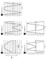
LED等の発光素子を用いた固体走査系の露光デバイスは、発光素子を列状に並べた発光素子アレイと、ロッドレンズやその他のレンズ等を列状に並べたレンズアレイとから構成される。このような露光デバイスでは、並べられた発光素子とレンズとの位置関係に依存して照射光量(感光体表面が受光する光量)の変化が生じる。そのため、レンズの半径(或いはその整数倍)周期の濃度ムラが生じてしまう。例えば、図3(a)及び図3(b)は、発光素子にLED、レンズにロッドレンズを用いた場合の、発光素子アレイとレンズアレイとの位置関係を表す模式図である。図3(a)及び図3(b)では、一列に並べられたLEDを夫々斜線入りの長方形で示し、ロッドレンズアレイの各ロッドレンズを白丸で描いてある。具体的には、半径200μm程度のロッドレンズが2段に重なりつつ並べられ、その中央に1200dpiピッチ即ち21.1μmピッチでLEDが並べられた配置関係を図示している。各LEDはロッドレンズアレイに対する位置関係が異なり、ロッドレンズのどの箇所をLEDからの光が通過するかに依存して光量損失等が異なることから、並べられたLEDとロッドレンズとの位置関係に依存して照射光量の変化が生じる。 An exposure device of a solid scanning system using light emitting elements such as LEDs is composed of a light emitting element array in which light emitting elements are arranged in a row and a lens array in which rod lenses and other lenses are arranged in a row. In such an exposure device, the amount of irradiation light (the amount of light received by the surface of the photoreceptor) varies depending on the positional relationship between the arranged light emitting elements and the lens. For this reason, density unevenness occurs with a period of the radius of the lens (or an integer multiple thereof). For example, FIGS. 3A and 3B are schematic diagrams showing the positional relationship between the light emitting element array and the lens array when an LED is used as the light emitting element and a rod lens is used as the lens. In FIG. 3A and FIG. 3B, the LEDs arranged in a row are indicated by hatched rectangles, and each rod lens of the rod lens array is drawn by a white circle. More specifically, the arrangement relationship is shown in which rod lenses having a radius of about 200 μm are arranged in two stages, and LEDs are arranged at the center at a 1200 dpi pitch, that is, 21.1 μm pitch. Each LED has a different positional relationship with the rod lens array, and the amount of light loss etc. varies depending on which part of the rod lens the light from the LED passes through. Depending on this, the amount of irradiation light changes.
このような固体走査系露光デバイスにおける長手方向ムラを低減させるために、初期状態において、LEDアレイとロッドレンズアレイとの位置関係に起因する光照射分布ムラを計測した上で、駆動電流量を調整することが想定される。しかし、このような調整を行った場合であっても、使用時の発熱による光学部品の変形等が生じた場合には、LEDアレイとロッドレンズアレイとの相対位置関係がずれるため、各素子に対応する感光体面上の照射光量も変化してしまう。従って、初期調整時に計測した光照射分布ムラを用いては、駆動電流量の補正を適切に実行することが出来なくなる。 In order to reduce unevenness in the longitudinal direction of such a solid-state scanning exposure device, in the initial state, the light irradiation distribution unevenness caused by the positional relationship between the LED array and the rod lens array is measured, and then the drive current amount is adjusted. It is assumed that However, even when such adjustments are made, if the optical components are deformed due to heat generation during use, the relative positional relationship between the LED array and the rod lens array shifts. The amount of light irradiated on the corresponding photoreceptor surface also changes. Therefore, it is impossible to appropriately correct the drive current amount by using the light irradiation distribution unevenness measured at the time of initial adjustment.
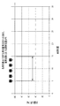
例えば、図3(a)に示すような状態を初期状態とし、この配置において発生する光量ムラを解消する調整を行ったとしても、使用による発熱や経時変化により図3(b)に示すような配置に変わってしまうことが想定される。図中、白抜き数字が指し示す各LEDについて、図3(a)から図3(b)への状態変化に伴い、レンズに対する相対位置が変化している。すると、図4に示すような照射光量ばらつきが生じてしまい、ドット光量分布に応じた画像スジ(濃度ムラ)が発生してしまう。ここで、図4の横軸はLEDアレイが伸びる方向と同方向における画素位置であり、縦軸は(画素位置に対する)感光体表面における照射光量である。尚、照射光量はベタ画像照射時の光量を100%として、正規化した光量比率である。 For example, even if the state shown in FIG. 3A is set as the initial state and adjustment for eliminating the unevenness in the amount of light generated in this arrangement is performed, the heat generated by use and the change over time are used as shown in FIG. It is assumed that the layout will change. In the figure, for each LED indicated by the white numbers, the relative position with respect to the lens changes with the change in state from FIG. 3 (a) to FIG. 3 (b). Then, the irradiation light amount variation as shown in FIG. 4 occurs, and an image stripe (density unevenness) corresponding to the dot light amount distribution occurs. Here, the horizontal axis in FIG. 4 is the pixel position in the same direction as the direction in which the LED array extends, and the vertical axis is the irradiation light amount on the surface of the photoreceptor (relative to the pixel position). The irradiation light amount is a normalized light amount ratio with the light amount upon solid image irradiation being 100%.
そこで本発明では、発光素子アレイとレンズアレイとの間で相対位置関係の変化があった場合においても、安定して均一な光照射を行うことが可能な高品位の画像形成装置を実現することを目的とする。 Therefore, the present invention realizes a high-quality image forming apparatus capable of performing stable and uniform light irradiation even when the relative positional relationship between the light emitting element array and the lens array changes. With the goal.
本発明は、発光素子アレイ及びレンズアレイから成る光学ヘッドを備えた、電子写真方式の画像形成装置であって、複数の画像パッチを形成する形成手段と、前記複数の画像パッチの、各濃度値を取得する取得手段と、前記取得した各濃度値に基づき、前記発光素子アレイを構成する各発光素子に対する発光量補正量を導出する導出手段とを備え、前記複数の画像パッチは夫々異なり、前記レンズアレイを構成するレンズの半径に相当する長手方向における画素群のうちの一部の画素に対して光を照射することで形成されることを特徴とする。 The present invention relates to an electrophotographic image forming apparatus including an optical head composed of a light emitting element array and a lens array, and forming means for forming a plurality of image patches, and density values of the plurality of image patches. And obtaining means for deriving a light emission amount correction amount for each light-emitting element constituting the light-emitting element array based on each acquired density value, wherein the plurality of image patches are different from each other, and It is formed by irradiating a part of the pixels in the longitudinal direction corresponding to the radius of the lens constituting the lens array with light.
本発明により、発光素子アレイとレンズアレイとの間の相対位置が初期状態からずれた場合においても、適正な補正を行う高品位な画像形成装置を実現することが出来る。 According to the present invention, it is possible to realize a high-quality image forming apparatus that performs appropriate correction even when the relative position between the light-emitting element array and the lens array deviates from the initial state.
以下、添付の図面を参照して、本発明をその好適な実施例に基づいて詳細に説明する。尚、以下の実施例において示す構成は例示に過ぎず、本発明は図示された構成に限定されるものではない。 Hereinafter, the present invention will be described in detail based on preferred embodiments with reference to the accompanying drawings. In addition, the structure shown in the following Examples is only an illustration, and this invention is not limited to the structure shown in figure.
[実施例1]
本実施例に係る画像形成装置は、複数並べた発光素子(LED)を点灯し、ロッドレンズアレイを介して像担持体たる感光体ドラムに光潜像を形成する電子写真方式の画像形成装置である。画像形成装置は、並べられた発光素子(LED)のうちの各点灯素子(点灯しているLED)の発光量を調整するため、特定の発光素子(LED)のみを点灯させることによって形成可能な複数の画像パッチを、感光体ドラム表面に形成する。画像パッチとは、画像の細かい部分領域である。複数の画像パッチそれぞれは、部分領域において照射される画素位置と照射されない画素位置を含む。ここで、各画素位置は、少なくとも1つ以上の発光素子(LED)に対応している。形成される複数の画像パッチのパターンは夫々、感光体ドラム長手方向における照射される画素の位置が異なり、発光素子(LED)の位相が異なるという特徴を有する。
[Example 1]
The image forming apparatus according to the present embodiment is an electrophotographic image forming apparatus that turns on a plurality of light emitting elements (LEDs) and forms a light latent image on a photosensitive drum as an image carrier via a rod lens array. is there. The image forming apparatus can be formed by lighting only a specific light emitting element (LED) in order to adjust the light emission amount of each lighting element (lighted LED) among the arranged light emitting elements (LED). A plurality of image patches are formed on the surface of the photosensitive drum. An image patch is a fine partial area of an image. Each of the plurality of image patches includes a pixel position irradiated in the partial region and a pixel position not irradiated. Here, each pixel position corresponds to at least one light emitting element (LED). The patterns of the plurality of image patches to be formed are characterized in that the positions of the irradiated pixels in the longitudinal direction of the photosensitive drum are different and the phases of the light emitting elements (LEDs) are different.
(全体構成)
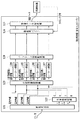
本実施例に係る画像形成装置は、画像データを生成する画像処理部(図1参照)と、当該画像データに基づいて実際に印刷を実行する画像形成部(図2参照)とから構成される。
(overall structure)
The image forming apparatus according to this embodiment includes an image processing unit (see FIG. 1) that generates image data and an image forming unit (see FIG. 2) that actually executes printing based on the image data. .
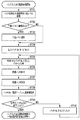
(画像処理部)
画像処理部が行う処理について、図1を用いて説明する。本実施例に係る画像処理部は、不図示のPC等の機器から出力されたプリンタ記述言語(以下「PDL」という)等で記述された画像出力命令を受信すると、一般的な電子写真画像形成装置と同じく、画像生成部101にてラスタライズを行う。ラスタライズ後、画像生成部101は、RGB画像情報を色変換処理部102に送り、属性情報を分版画像記憶部103に送る。色変換処理部102は、RGB画像情報をCMYK画像情報に変換する色変換処理を行い、CMYK画像情報を分版画像記憶部103に送る。次いで、分版画像記憶部103から、CMYKの版毎の画像情報及び属性情報が版毎のハーフトーン処理部104〜107に送られる。ハーフトーン処理部104はC版画像情報に対するハーフトーン処理を実行する。同様に、ハーフトーン処理部105〜107は、MYK画像情報に対するハーフトーン処理を実行する。次いで、ハーフトーン処理後のハーフトーン画像はハーフトーン画像記憶部108に一時格納された上で、転送用バッファ116に格納される。画像形成部が送出するタイミング信号に同期して、画像データ転送部117は、転送用バッファ116から受信したハーフトーン画像を画像形成部に対して転送する。
(Image processing unit)
Processing performed by the image processing unit will be described with reference to FIG. When the image processing unit according to the present embodiment receives an image output command described in a printer description language (hereinafter referred to as “PDL”) output from a device such as a PC (not shown), a general electrophotographic image formation is performed. As with the apparatus, the
(画像形成部)
画像形成部について、図2を用いて説明する。画像処理部により生成され、画像処理部から画像形成部に出力された画像データに基づき、画像形成部は、印刷を実行する。
(Image forming part)
The image forming unit will be described with reference to FIG. Based on the image data generated by the image processing unit and output from the image processing unit to the image forming unit, the image forming unit executes printing.
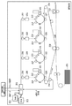
画像形成部は、画像データに基づき、駆動回路204〜207によりLEDアレイとロッドレンズアレイとを一体化させた各色の光学ヘッド208〜211を駆動させる。具体的には、駆動回路204〜207により光学ヘッド208〜211に駆動電流を供給し、LEDアレイを構成するLEDを点灯させ、ロッドレンズアレイを介して等倍結合させる。これにより、帯電器216〜219によって帯電された、像担持体である感光体ドラム212〜215上に露光像を結像させ、感光体ドラム表面に電荷潜像を形成する。以上、露光により感光体ドラム表面に電荷潜像を形成するまでの工程を、露光工程と定義する。
The image forming unit drives the
露光工程後の現像工程では、感光体ドラム表面に形成された電荷潜像を、現像器220〜223からの現像剤(以下、「トナー」という)によってトナー像として現像(顕在化)する。
In the development process after the exposure process, the charge latent image formed on the surface of the photosensitive drum is developed (made visible) as a toner image by a developer (hereinafter referred to as “toner”) from the developing
現像工程後の一次転写工程では、感光体ドラム212〜215と転写ベルト228との当接部において、転写手段として機能する導電ローラ224〜227による電圧印加が行われることで、トナー像を感光体ドラム上から転写ベルト上へと一次転写する。一次転写により、転写ベルト上に、シアン像、マゼンダ像、イエロー像、ブラック像等の各色像を、同期を取って順次形成することでフルカラー像を形成する。
In the primary transfer step after the development step, voltage application is performed by the
一次転写工程後の二次転写工程では、転写ベルトと転写材である記録媒体(用紙等)230とが当接する二次転写ニップにおいて、二次転写ローラ229による電圧印加が行われることで、フルカラーのトナー像を転写ベルト上から転写材上へと二次転写する。尚、転写材である記録媒体230は、給紙カセット231に格納されており、印刷指示に基づき、順次給紙される。
In the secondary transfer process after the primary transfer process, a voltage is applied by the
フルカラーのトナー像が表面に形成された転写材(記録媒体)は、定着手段へと搬送され、転写材及び転写材上のトナー像に対して、加熱された定着ローラ232が熱及び圧力を印加し、トナー像を転写材上に溶融定着する。最終的に、トナー像定着によりフルカラー画像が描画された記録媒体は、排出部へと送られ機器外へ排出される。
The transfer material (recording medium) on which the full-color toner image is formed is conveyed to the fixing unit, and the
(LEDアレイに対する初期光量調整)
一般的なLEDアレイでは、LED毎に発光特性(具体的には発光効率)が異なる。従って、初期組み立て・調整時に各LEDの発光量を計測した上で、各LEDの発光量を均一化するための発光量補正量(例えば、初期状態で基準とする駆動電流量等)をLED毎に記憶する。そして、記憶された発光量補正量に従って、LEDアレイは制御される。
(Initial light intensity adjustment for LED array)
In a general LED array, the light emission characteristics (specifically, light emission efficiency) are different for each LED. Therefore, after measuring the light emission amount of each LED at the time of initial assembly and adjustment, the light emission amount correction amount (for example, the drive current amount used as a reference in the initial state) for each LED is made uniform for each LED. To remember. Then, the LED array is controlled according to the stored light emission amount correction amount.
(LEDアレイとロッドレンズアレイとの間の位置ずれが生じさせる照射光量ムラ)
LEDから発光された光を、ロッドレンズを介して等倍で感光体ドラム表面に結像させたとき、LEDのロッドレンズアレイに対する位置により、各LEDに対応した光スポットの形状・光量は変化する。このLEDアレイとロッドレンズアレイとの相対位置ずれに依存する光スポットの形状変化及び光量変化は、LEDとロッドレンズとの間の焦点深度方向の位置ずれが大きいほど、より顕著に現れる。
(Irradiation amount unevenness caused by misalignment between LED array and rod lens array)
When the light emitted from the LED is focused on the surface of the photoconductive drum through the rod lens at the same magnification, the shape and light quantity of the light spot corresponding to each LED changes depending on the position of the LED with respect to the rod lens array. . The change in the shape and light amount of the light spot depending on the relative positional deviation between the LED array and the rod lens array appears more prominently as the positional deviation in the focal depth direction between the LED and the rod lens increases.
LEDアレイを構成するLEDの長時間に亘る連続点灯に伴う発熱等によりLEDアレイの形状は変化する。これにより、LEDアレイとロッドレンズアレイとの間の相対位置関係も変化する。この相対位置関係の変化に起因する光スポットの形状変化及び光量変化によって引き起こされる照射光量ムラは、経時的に発生するものである。よって、初期調整を行ったとしても、印刷画像における濃度ムラの発生を防ぐことは出来ない。 The shape of the LED array changes due to heat generated by continuous lighting of the LEDs constituting the LED array for a long time. As a result, the relative positional relationship between the LED array and the rod lens array also changes. Irradiation light amount unevenness caused by the light spot shape change and light amount change caused by the change in the relative positional relationship occurs over time. Therefore, even if the initial adjustment is performed, the occurrence of density unevenness in the printed image cannot be prevented.
そのため、LEDアレイの長時間に亘る連続点灯に伴う発熱等によりLEDアレイとロッドレンズアレイとの間で相対位置関係が変化した場合、ロッドレンズ半径を周期とする濃度ムラが生じてしまう。その結果、画像送り方向に伸びる画像スジが発生してしまう、という課題が生じる。 Therefore, when the relative positional relationship changes between the LED array and the rod lens array due to heat generated by continuous lighting of the LED array for a long time, density unevenness with a period of the rod lens radius occurs. As a result, there arises a problem that an image streak extending in the image feeding direction is generated.
例えば、半径211μmのロッドレンズを配列したロッドレンズアレイに対し1200dpiピッチ即ち21.1μmピッチで配列したLEDを使用する光学系にて長時連続出力を行った場合、1200dpiで10ドット周期に相当する間隔の濃度ムラが発生する。 For example, when continuous output is performed for a long time in an optical system using LEDs arranged at a pitch of 1200 dpi or 21.1 μm for a rod lens array in which rod lenses with a radius of 211 μm are arranged, an interval corresponding to a period of 10 dots at 1200 dpi Density unevenness occurs.
(ロッドレンズ半径に相当する周期を有する光量ムラを推定するための、画像パッチの出力及び読取)
本実施例の画像形成装置は、経時的に生じたLEDアレイとロッドレンズアレイと間の相対位置ずれに起因する濃度ムラを防ぐため、ロッドレンズ半径の整数倍間隔に存在する画素のうちの1画素のみ照射する画像パッチを5種出力(感光体ドラム表面に形成)する。5種の画像パッチは夫々、点灯する発光素子(LED)の位相(位置)が異なるものである。出力されたパッチ群をパッチ検250で読み取った読取結果を用いて、ロッドレンズ半径を周期とするムラの振幅及び位相を推定する。そして、推定結果を用いて、発光量補正量として各LEDに対する駆動電流量が保持されるテーブルの値を更新する。尚、パッチ検とは、感光体ドラム上に載ったトナーに光を当て、その光の反射レベルから反射濃度を測定する検知機のことである。
(Output and reading of an image patch for estimating the amount of light unevenness having a period corresponding to the rod lens radius)
The image forming apparatus according to the present exemplary embodiment is configured so that one of the pixels existing at intervals of an integer multiple of the rod lens radius is used in order to prevent density unevenness due to the relative positional deviation between the LED array and the rod lens array that occurs with time. Five types of image patches that irradiate only the pixels are output (formed on the surface of the photosensitive drum). Each of the five types of image patches has different phases (positions) of light emitting elements (LEDs) to be lit. Using the read result obtained by reading the output patch group by the
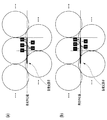
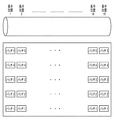
図5は、本実施例に係る画像形成装置において感光体ドラム表面に形成される5種の画像パッチを示す図である。本実施例では、縦8画素×横10画素の矩形である画像パッチを5種類出力する。本実施例では、ロッドレンズ半径が10画素に相当するため、5種の画像パッチは何れも長手方向10画素につき1画素照射されるパターンを有する点で同じである。ただし、5種のパターンを形成する際に点灯する、発光素子(LED)のロッドレンズに対する位相(位置)が夫々異なる。5種のパターンにおいて照射される画素に対応する各発光点がロッドレンズアレイのどの位置にあるかを示した図が、図6である。図6中の白抜き数字1〜5は、発光点を示す。発光点とは、発光中心線上における発光素子の位置である。図6は図3(a)と同様の図であるが、図5に示した画像パッチを出力する際に点灯する発光点(発光素子)とロッドレンズアレイとの位置関係を示している。図6中の発光素子(LED)アレイ及びロッドレンズアレイは、図3(a)と同様である。
FIG. 5 is a diagram showing five types of image patches formed on the surface of the photosensitive drum in the image forming apparatus according to the present embodiment. In the present embodiment, five types of image patches each having a rectangular shape of 8 vertical pixels × 10 horizontal pixels are output. In the present embodiment, since the radius of the rod lens corresponds to 10 pixels, the five types of image patches are the same in that each has a pattern in which one pixel is irradiated for every 10 pixels in the longitudinal direction. However, the phases (positions) of the light emitting elements (LEDs) with respect to the rod lenses, which are turned on when five types of patterns are formed, are different. FIG. 6 is a diagram showing in which position of the rod lens array each light emitting point corresponding to the pixel irradiated in the five types of patterns.
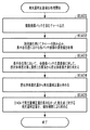
(画像パッチの出力及び読取処理)
画像形成部によって実行される画像パッチの出力及び読取処理について、図7を用いて説明する。
(Image patch output and reading processing)
Image patch output and reading processing executed by the image forming unit will be described with reference to FIG.
ステップS701(以下、「S701」と略記し、他のステップも同様に略記する)において、CPU201は、パッチ検250(の発光部)を発光させる。パッチ検250は、感光体ドラム上で反射された光を計測してバックグランド(下地)レベルを読み取る。尚、バックグランド(下地)レベルとは、感光体ドラムでトナーが載っていない箇所からの光の反射レベルである。次いで、処理はS702に進む。
In step S701 (hereinafter abbreviated as “S701” and the other steps are also abbreviated in the same manner), the
S702において、CPU201は、読み取った下地レベルに異常があるか否かを、閾値と比較すること等により判定する。感光体ドラム表面に傷がある場合等に、下地レベルに異常が生じる。判定の結果、下地レベルに異常がある場合、処理はS703に進み、下地レベルに異常が無い場合、処理はS704に進む。
In step S <b> 702, the
S703において、CPU201は、パッチ検の測定値におけるオフセット成分を除去するために下地レベルの値を更新する。次いで、処理はS704に進む。
In step S <b> 703, the
S704において、CPU201は、これから出力するパッチのパッチNoを1にセットする。次いで、処理はS705に進む。
In step S <b> 704, the
S705において、CPU201は、セットされたパッチNoに対応するパターンをROM203から取得する。次いで、処理はS706に進む。
In step S <b> 705, the
S706において、CPU201は、取得したパターンに従った露光・現像により感光体ドラム表面上に画像パッチを形成する。次いで、処理はS707に進む。
In step S706, the
S707において、CPU201は、感光体ドラム表面上に形成された画像パッチをパッチ検250により読み取って、濃度値を取得する。次いで、処理はS708に進む。
In step S <b> 707, the
S708において、CPU201は、S707で取得した濃度値をパッチNo‐濃度テーブルに保存する。次いで、処理はS709に進む。
In step S708, the
S709において、CPU201は、全種のパッチ出力及び読取が終了したか否かを判定する。判定の結果、全種のパッチ出力及び読取が終了した場合、一連の処理を終了し、そうでない場合、処理はS710に進む。
In step S709, the
S710において、CPU201は、パッチNoをインクリメントする。次いで、処理はS705に戻る。
In S710, the
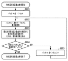
(発光量補正量導出処理)
画像形成部によって実行される発光量補正量導出処理について、図8を用いて説明する。
(Light emission amount correction amount derivation process)
The light emission amount correction amount derivation process executed by the image forming unit will be described with reference to FIG.
S801において、CPU201は、着目するパッチのパッチNoを1にセットする。次いで、処理はS802に進む。
In step S <b> 801, the
S802において、CPU201は、パッチNo‐濃度テーブルから着目するパッチのパッチNoに対応する濃度値を読み取る。次いで、処理はS803に進む。
In step S <b> 802, the
S803において、CPU201は、S802で読み取った濃度値に対応する感光体表面光量を、図15に示すような感光体表面光量‐濃度の関係を用いて求める。そして、感光体表面光量から、対応する発光素子に対する発光量補正量として駆動電流量を求める。駆動電流量は、感光体表面光量から一義的に求めることが出来る。駆動電流量は、対応する発光素子に対する発光量補正量として保存される。次いで、処理はS804に進む。
In step S <b> 803, the
S804において、CPU201は、全種のパッチについて、発光量補正量導出処理が終了したか否か判定する。判定の結果、全種のパッチについて、発光量補正量導出処理が終了した場合、一連の処理を終了し、そうでない場合、処理はS805に進む。
In step S804, the
S805において、CPU201は、着目するパッチのパッチNoをインクリメントする。次いで、処理はS802に戻る。
In step S805, the
上記の処理では、感光体ドラム表面上に形成された画像パッチをパッチ検が読み取った結果に基づき、感光体ドラム表面を照射する照射光量が初期調整時よりも増加、或いは、減少したかを判定している。照射光量が初期調整時より減少したと判定された場合(即ち「薄い」と判定された場合)、画像パッチを形成する際に発光したLEDに対する駆動電流量を増加させることで、LEDの発光量を増加させる。一方、照射光量が初期調整時より増加したと判定された場合(即ち「濃い」と判定された場合)、画像パッチを形成する際に発光したLEDに対する駆動電流量を減少させることで、LEDの発光量を減少させる。 In the above processing, based on the result of patch detection of the image patch formed on the surface of the photosensitive drum, it is determined whether the amount of irradiation light irradiating the surface of the photosensitive drum has increased or decreased compared to the initial adjustment. doing. If it is determined that the amount of irradiation light has decreased from the initial adjustment (ie, if it is determined to be “thin”), the amount of light emitted from the LED can be increased by increasing the amount of drive current for the LED that was emitted when forming the image patch Increase. On the other hand, when it is determined that the irradiation light amount has increased from the time of initial adjustment (ie, when it is determined to be “deep”), the amount of drive current for the LED that emits light when the image patch is formed is reduced, thereby Reduce the amount of luminescence.
(発光素子(LED)に対する駆動電流量の補正)
5種の画像パッチは点灯させる発光素子の位相が異なる。即ち、パッチ1を基準にすると、パッチ2〜5では、パッチ1で照射される画素に対して2画素、4画素、6画素、8画素長手方向にずらした画素位置に対応する発光点が点灯している(図5参照)。
パッチ1:基準位相の発光点のみ点灯
パッチ2:パッチ1で照射される画素に対し2画素長手方向にずらした画素位置に対応する発光点のみ点灯
パッチ3:パッチ1で照射される画素に対し4画素長手方向にずらした画素位置に対応する発光点のみ点灯
パッチ4:パッチ1で照射される画素に対し6画素長手方向にずらした画素位置に対応する発光点のみ点灯
パッチ5:パッチ1で照射される画素に対し8画素長手方向にずらした画素位置に対応する発光点のみ点灯
(Correction of drive current amount for light emitting element (LED))
The five types of image patches have different phases of light emitting elements to be lit. That is, on the basis of the
Patch 1: Lights only at the light emission point of the reference phase Patch 2: Lights only at the light emission point corresponding to the pixel position shifted in the longitudinal direction by 2 pixels with respect to the pixel irradiated with the
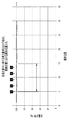
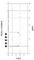
図9は、S707で取得した各パッチに対する濃度値から図15の関係を用いて導出することが可能な、感光体ドラム長手方向画素位置における照射光量分布を示すグラフである。図9からは、発光点1〜5に対応する画素位置における照射光量は均一でなく、高低があることが確認される。そこで本実施例では、図10に示すような発光量補正量を適用することで、図9に示したような照射光量のばらつきを打ち消す。図10の縦軸は発光量補正量である。発光量補正量が100%以上で多いほど、発光素子の発光量を増やすために駆動電流量は増加する。発光量補正量が100%未満で少ないほど、発光素子の発光量を減らすために駆動電流量は減少する。発光量補正後の結果を図11に示す。図11から、感光体表面上に照射される光量の不均一さは減少していることが確認できる。
FIG. 9 is a graph showing the irradiation light amount distribution at the pixel position in the longitudinal direction of the photosensitive drum, which can be derived from the density value for each patch acquired in S707 using the relationship of FIG. From FIG. 9, it is confirmed that the amount of irradiation light at the pixel positions corresponding to the
尚、上述した図5の例では、5個の発光点(即ち発光点1〜5)と対応する画素1〜5についてのみ説明を行った。ここで、ロッドレンズ半径を周期(=10画素周期)として、パッチ1〜パッチ5を用いて推測されるムラの振幅が繰り返されていることにより、その他の画素を含んだ全ての画素についての照射光量補正が可能となる。即ち、全ての発光素子はパッチ1〜5(正確にはパッチ1〜5から取得した結果を線形補間した結果)の何れかと対応する。従って、全ての発光素子は、パッチ1〜5から取得した結果を線形補間した結果の何れかと対応する発光素子と同位相である。よって、パッチ1〜5から導出可能な10個の画素位置に対応する発光素子に対する発光量補正量を用いることで、均一な照射光量分布を得ることが可能となる。図11に白抜き数字で示す発光点1〜5と対応する画素位置以外の画素位置に存在する画素が、上述した「その他の画素」であり、発光点1〜5と対応する画素同様に、発光素子に対する発光量(駆動電流量)の補正処理が行われる。
In the example of FIG. 5 described above, only the
以上説明したように、本実施例の画像形成装置は、ロッドレンズ半径に相当する画素群のうちの一部の画素(本実施例では1画素)のみを照射する複数の画像パッチを、出力し、当該出力を読み取る。出力される複数の画像パッチは夫々、位相が異なる発光素子が点灯することにより形成される。また、本実施例の画像形成装置は、画像パッチの読み取り値を用いて、発光素子とロッドレンズアレイとの相対位置に応じて異なる発光量補正量を、各発光素子に適用する。これにより、発光素子のロッドレンズアレイに対する相対位置において長手方向にずれが生じている場合であっても、適正な補正を行う高品位な画像形成装置を実現することが出来る。 As described above, the image forming apparatus according to the present exemplary embodiment outputs a plurality of image patches that irradiate only a part of pixels (one pixel in the present exemplary embodiment) in the pixel group corresponding to the rod lens radius. Read the output. Each of the plurality of output image patches is formed by turning on light emitting elements having different phases. In addition, the image forming apparatus according to the present exemplary embodiment applies a light emission amount correction amount that varies depending on the relative position between the light emitting element and the rod lens array to each light emitting element, using the read value of the image patch. As a result, it is possible to realize a high-quality image forming apparatus that performs appropriate correction even when there is a shift in the longitudinal direction at the relative position of the light emitting element to the rod lens array.
尚、上記の例では、レンズアレイとしてロッドレンズアレイを用いた場合を例に挙げて説明したが、レンズアレイはロッドレンズアレイに限定されない。一般的なレンズを組み合わせた光学系を複数並べたレンズアレイを介して、発光素子アレイからの光を感光体表面に結像させるものであれば本願と同様な課題が生じるので、本実施例を有効に適用することが出来る。 In the above example, the case where a rod lens array is used as the lens array has been described as an example, but the lens array is not limited to the rod lens array. If the light from the light emitting element array is imaged on the surface of the photoreceptor through a lens array in which a plurality of optical systems combined with general lenses are arranged, the same problem as in the present application occurs. It can be applied effectively.
[実施例2]
本実施例の画像形成装置は、感光体ドラム長手方向における複数位置において、実施例1と同様の複数の画像パッチを形成し、用紙を印刷出力する。そして、出力した画像パッチをリーダーで読み取る。尚、感光体ドラム長手方向における各位置において形成される複数の画像パッチのパターンは夫々、感光体ドラム長手方向における照射される画素の位置が異なり、点灯させる発光素子(LED)の位相(位置)が異なることは実施例1と同様である。
[Example 2]
The image forming apparatus according to the present exemplary embodiment forms a plurality of image patches similar to the first exemplary embodiment at a plurality of positions in the longitudinal direction of the photosensitive drum, and prints out a sheet. The output image patch is read by a reader. Note that the pattern of the plurality of image patches formed at each position in the longitudinal direction of the photosensitive drum is different in the position of the irradiated pixel in the longitudinal direction of the photosensitive drum, and the phase (position) of the light emitting element (LED) to be lit. Is the same as in the first embodiment.
本実施例では、LEDアレイとロッドレンズアレイとの間の相対位置ずれに起因する濃度ムラが周期性を有さない場合を想定している。 In the present embodiment, it is assumed that the density unevenness caused by the relative positional deviation between the LED array and the rod lens array has no periodicity.
尚、本実施例は、発光量補正量導出手順が異なること以外は、実施例1と同様である。ただし本実施例では、複数の画像パッチを含むチャートを用紙に印刷し、出力用紙の読取手段として、図2では不図示のリーダーを用いている。 This embodiment is the same as the first embodiment except that the light emission amount correction amount derivation procedure is different. However, in this embodiment, a chart including a plurality of image patches is printed on a sheet, and a reader (not shown in FIG. 2) is used as an output sheet reading unit.
(長手方向の各位置によって異なる、LEDアレイとロッドレンズアレイとの間の相対位置ずれの程度)
ロッドレンズに対する発光素子(LED)の位置(距離)は、発熱や経時変化などによって、長手位置の領域毎に異なる変位が生じてしまうことがある。その場合、長手各位置において、対応する発光素子の位相に対するずれ量は異なるものとなる。
(The degree of relative positional deviation between the LED array and the rod lens array, which varies depending on the position in the longitudinal direction)
The position (distance) of the light emitting element (LED) with respect to the rod lens may vary depending on the region of the longitudinal position due to heat generation or change with time. In that case, the shift amount with respect to the phase of the corresponding light emitting element is different at each longitudinal position.
そのような変位・ずれが生じた場合に、実施例1に係る長手内の1箇所における画像パッチの形成・読取を行った上で、その読取値を用いた長手全域の補正を行ってしまうと問題が生じる。即ち、長手各位置において、各発光素子の位相のずれ方向が異なっている場合や、ずれ方向は同じでもずれ量が大きく異なっている場合が想定され、これらのような場合に感光体表面上における照射光量ムラを補正前より顕在化させてしまう恐れがある。 When such a displacement / displacement occurs, if the image patch is formed and read at one location in the longitudinal direction according to the first embodiment and then the entire longitudinal length is corrected using the read value. Problems arise. That is, it is assumed that the phase shift direction of each light emitting element is different at each longitudinal position, or that the shift direction is the same but the shift amount is greatly different. There is a risk that the unevenness in the amount of irradiated light will become apparent before correction.
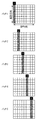
長手各位置において、LEDアレイとロッドレンズアレイとの間の相対位置ずれの程度が異なってくる場合について、図12を用いて説明する。図12の横軸は、感光体ドラムの長手方向において画像パッチを形成した位置である(図13参照)。縦軸は、感光体表面における照射光量の理想値からのずれである。例えば、図12のパッチ1では、光量ずれの方向こそ長手位置に依らずに一定であるが、光量ずれの大きさは長手位置に応じて異なってくる。また、パッチ2では、長手位置に応じて光量ずれの方向すら異なってくる。従って、長手中央(1箇所)に形成したパッチを用いて光量補正量を導出し、その光量補正量を感光体ドラム長手方向全域に適用した場合、各画素間の光量を均一化するどころか、むしろムラを顕在化させてしまうことになる。
A case where the degree of relative positional deviation between the LED array and the rod lens array varies at each longitudinal position will be described with reference to FIG. The horizontal axis in FIG. 12 is the position where the image patch is formed in the longitudinal direction of the photosensitive drum (see FIG. 13). The vertical axis represents the deviation from the ideal value of the amount of irradiation light on the surface of the photoreceptor. For example, in the
(長手位置19箇所における画像パッチ出力、読取、及び発光素子に対する発光量補正)
そこで本実施例では、図13に示すように、長手位置19箇所で5種の画像パッチ(パッチ1〜パッチ5)を形成し、印刷出力及び読取を行う。これにより、長手各位置における各パッチと対応する発光素子に対して適切な発光量(駆動電流量)補正が可能となる。本実施例に係る発光量補正量導出処理について、図14を用いて説明する。
(Image patch output at 19 longitudinal positions, reading, and light emission amount correction for light emitting elements)
Therefore, in this embodiment, as shown in FIG. 13, five types of image patches (
S1401において、CPU201は、長手位置19箇所で5種の画像パッチが形成されたチャートを印刷出力する。次いで、処理はS1402に進む。
In step S1401, the
S1402において、CPU201は、図2では不図示のリーダーによりチャートを読み取って、長手各位置における各画像パッチの濃度値を取得する。次いで、処理はS1403に進む。
In step S1402, the
S1403において、CPU201は、S1402で取得した濃度値に対応する感光体表面光量を、実施例1と同様に、図15に示すような感光体表面光量‐濃度の関係を用いて求める。次いで、処理はS1404に進む。
In step S1403, the
S1404において、CPU201は、実施例1と同様に、感光体表面光量から、発光量補正量としてLEDに対する駆動電流量を一義的に求める。次いで、処理はS1405に進む。
In step S <b> 1404, as in the first embodiment, the
S1405において、S1404で発光量補正量を求めなかった発光点に対する発光量補正量を、当該発光点と近接し且つ発光量補正量を求めた発光点に対する発光量補正量を用いた線形補間により求める。 In S1405, the light emission amount correction amount for the light emission point for which the light emission amount correction amount was not obtained in S1404 is obtained by linear interpolation using the light emission amount correction amount for the light emission point that is close to the light emission point and for which the light emission amount correction amount was obtained. .
(長手方向のムラ(画像送り方向に伸びている画像スジ)解消効果)
本実施例では、図13に示したような長手位置19箇所で5種の画像パッチを形成し、印刷出力及び読取を行う。また、画像パッチを形成しない箇所(19箇所以外の箇所)については、最近接の2か所における出力・読取の結果を用いた線形補間により、発光量補正量を算出する。これにより、感光体ドラム長手方向全画素に対する適切な照射光量補正が可能となる。
(Elimination of unevenness in the longitudinal direction (image streaks extending in the image feed direction))
In this embodiment, five types of image patches are formed at 19 longitudinal positions as shown in FIG. 13, and printed out and read. In addition, for locations where image patches are not formed (locations other than 19 locations), the light emission amount correction amount is calculated by linear interpolation using the output / read results at the two closest locations. Thereby, it is possible to appropriately correct the irradiation light amount for all the pixels in the longitudinal direction of the photosensitive drum.
以上説明したように、本実施例では、実施例1と同様の画像パッチ形成及び読取を、感光体ドラム長手方向における複数箇所で行う。これにより、LEDアレイとロッドレンズアレイとの間の相対位置ずれが周期性を持たず、長手各位置でLEDアレイとロッドレンズアレイとの間の位置ずれの度合いが異なってくるような場合でも、適正な補正を行う高品位な画像形成装置を実現することが出来る。
As described above, in this embodiment, image patch formation and reading similar to those in
[その他の実施例]
本発明は、上述の実施形態の1以上の機能を実現するプログラムを、ネットワーク又は記憶媒体を介してシステム又は装置に供給し、そのシステム又は装置のコンピュータにおける1つ以上のプロセッサーがプログラムを読出し実行する処理でも実現可能である。また、1以上の機能を実現する回路(例えば、ASIC)によっても実現可能である。
[Other Examples]
The present invention supplies a program that realizes one or more functions of the above-described embodiments to a system or apparatus via a network or a storage medium, and one or more processors in a computer of the system or apparatus read and execute the program This process can be realized. It can also be realized by a circuit (for example, ASIC) that realizes one or more functions.
201・・・CPU
204〜207・・・駆動回路
208〜211・・・光学ヘッド
212〜215・・・感光体ドラム
216〜219・・・帯電器
220〜223・・・現像器
250・・・パッチ検
201 ... CPU
204 to 207, drive
Claims (9)
複数の画像パッチを形成する形成手段と、
前記複数の画像パッチの、各濃度値を取得する取得手段と、
前記取得した各濃度値に基づき、前記発光素子アレイを構成する各発光素子に対する発光量補正量を導出する導出手段と
を備え、
前記複数の画像パッチは夫々異なり、前記レンズアレイを構成するレンズの半径に相当する長手方向における画素群のうちの一部の画素に対して光を照射することで形成されることを特徴とする画像形成装置。 An electrophotographic image forming apparatus having an optical head composed of a light emitting element array and a lens array,
Forming means for forming a plurality of image patches;
Obtaining means for obtaining each density value of the plurality of image patches;
Derivation means for deriving a light emission amount correction amount for each light emitting element constituting the light emitting element array based on each acquired density value; and
The plurality of image patches are different from each other, and are formed by irradiating a part of pixels in a longitudinal direction corresponding to a radius of a lens constituting the lens array with light. Image forming apparatus.
複数の画像パッチを形成する形成ステップと、
前記複数の画像パッチの、各濃度値を取得する取得ステップと、
前記取得した各濃度値に基づき、前記発光素子アレイを構成する各発光素子に対する発光量補正量を導出する導出ステップと
を備え、
前記複数の画像パッチは夫々異なり、前記レンズアレイを構成するレンズの半径に相当する長手方向における画素群のうちの一部の画素に対して光を照射することで形成されることを特徴とする画像形成方法。 An image forming method executed by an electrophotographic image forming apparatus having an optical head composed of a light emitting element array and a lens array,
Forming step for forming a plurality of image patches;
An acquisition step of acquiring each density value of the plurality of image patches;
A derivation step of deriving a light emission amount correction amount for each light emitting element constituting the light emitting element array based on each acquired density value; and
The plurality of image patches are different from each other, and are formed by irradiating a part of pixels in a longitudinal direction corresponding to a radius of a lens constituting the lens array with light. Image forming method.
Priority Applications (1)
| Application Number | Priority Date | Filing Date | Title |
|---|---|---|---|
| JP2015000955A JP2016124231A (en) | 2015-01-06 | 2015-01-06 | Image forming apparatus, image forming method, and program |
Applications Claiming Priority (1)
| Application Number | Priority Date | Filing Date | Title |
|---|---|---|---|
| JP2015000955A JP2016124231A (en) | 2015-01-06 | 2015-01-06 | Image forming apparatus, image forming method, and program |
Publications (1)
| Publication Number | Publication Date |
|---|---|
| JP2016124231A true JP2016124231A (en) | 2016-07-11 |
Family
ID=56358654
Family Applications (1)
| Application Number | Title | Priority Date | Filing Date |
|---|---|---|---|
| JP2015000955A Pending JP2016124231A (en) | 2015-01-06 | 2015-01-06 | Image forming apparatus, image forming method, and program |
Country Status (1)
| Country | Link |
|---|---|
| JP (1) | JP2016124231A (en) |
Cited By (1)
| Publication number | Priority date | Publication date | Assignee | Title |
|---|---|---|---|---|
| JP2018043492A (en) * | 2016-09-16 | 2018-03-22 | コニカミノルタ株式会社 | Optical writing device and image formation apparatus |
-
2015
- 2015-01-06 JP JP2015000955A patent/JP2016124231A/en active Pending
Cited By (1)
| Publication number | Priority date | Publication date | Assignee | Title |
|---|---|---|---|---|
| JP2018043492A (en) * | 2016-09-16 | 2018-03-22 | コニカミノルタ株式会社 | Optical writing device and image formation apparatus |
Similar Documents
| Publication | Publication Date | Title |
|---|---|---|
| US8964256B2 (en) | Method of correcting streaks using exposure modulation and spatially varying TRCs | |
| US9897956B2 (en) | Image forming apparatus | |
| JP2016133721A (en) | Image processing apparatus, image processing method, and program | |
| CN116804838A (en) | Image forming apparatus having a plurality of image forming units | |
| JP2015174442A (en) | Image forming device | |
| US9268252B2 (en) | Image forming apparatus and method with additional exposure of photoreceptor drum based on cycle of screen | |
| JP6263777B2 (en) | Optical writing apparatus and image forming apparatus | |
| JP5930750B2 (en) | Image forming apparatus and image forming method | |
| JP6209771B2 (en) | Image forming apparatus | |
| JP2016124231A (en) | Image forming apparatus, image forming method, and program | |
| US12265339B2 (en) | Image forming apparatus, control method thereof, and storage medium for correcting variations in light amount from light source | |
| JP6024212B2 (en) | Method for manufacturing image forming apparatus, method for adjusting light amount of print head, and method for manufacturing process cartridge | |
| JP5315618B2 (en) | Light emission amount adjusting device for recording apparatus and light emission amount adjusting method for recording device | |
| JP6642053B2 (en) | Semiconductor laser drive device and image forming apparatus | |
| JP4816006B2 (en) | Print head and image forming apparatus | |
| US9558430B2 (en) | Image forming apparatus using filters to correct potential distribution on photoreceptor due to spot shape of emitted light | |
| US20150185675A1 (en) | Image forming apparatus and adjustment method therefor | |
| JP2007030383A (en) | Image forming apparatus and image forming method | |
| JP2018008488A (en) | Light source drive device, image formation apparatus and light amount control method | |
| JP4403744B2 (en) | Correction data generation apparatus and light quantity correction method for optical print head | |
| JP6128817B2 (en) | Image forming apparatus and image forming method | |
| JP2006256150A (en) | Image forming apparatus | |
| JP6611503B2 (en) | Image processing apparatus, image processing method, and program | |
| US20240069463A1 (en) | Image-forming apparatus, correction chart, and method | |
| JP2006255976A (en) | Image forming device, and control method for printing head |