JP2016075836A - Pixel circuit, method for driving the pixel circuit, and display device - Google Patents
Pixel circuit, method for driving the pixel circuit, and display device Download PDFInfo
- Publication number
- JP2016075836A JP2016075836A JP2014206933A JP2014206933A JP2016075836A JP 2016075836 A JP2016075836 A JP 2016075836A JP 2014206933 A JP2014206933 A JP 2014206933A JP 2014206933 A JP2014206933 A JP 2014206933A JP 2016075836 A JP2016075836 A JP 2016075836A
- Authority
- JP
- Japan
- Prior art keywords
- transistor
- terminal
- voltage
- pixel circuit
- electrically connected
- Prior art date
- Legal status (The legal status is an assumption and is not a legal conclusion. Google has not performed a legal analysis and makes no representation as to the accuracy of the status listed.)
- Pending
Links
- 238000000034 method Methods 0.000 title claims description 41
- 239000003990 capacitor Substances 0.000 claims abstract description 148
- 239000011159 matrix material Substances 0.000 claims description 7
- 238000010586 diagram Methods 0.000 description 21
- 238000001514 detection method Methods 0.000 description 19
- 239000010410 layer Substances 0.000 description 19
- 239000000758 substrate Substances 0.000 description 19
- 239000010408 film Substances 0.000 description 11
- 230000007423 decrease Effects 0.000 description 8
- 239000005394 sealing glass Substances 0.000 description 7
- 239000011521 glass Substances 0.000 description 6
- 230000014759 maintenance of location Effects 0.000 description 6
- 229910021420 polycrystalline silicon Inorganic materials 0.000 description 6
- 229920005591 polysilicon Polymers 0.000 description 6
- 229920001621 AMOLED Polymers 0.000 description 4
- 229910052751 metal Inorganic materials 0.000 description 4
- 239000002184 metal Substances 0.000 description 4
- XLOMVQKBTHCTTD-UHFFFAOYSA-N Zinc monoxide Chemical compound [Zn]=O XLOMVQKBTHCTTD-UHFFFAOYSA-N 0.000 description 2
- 230000015572 biosynthetic process Effects 0.000 description 2
- 230000000694 effects Effects 0.000 description 2
- 238000005516 engineering process Methods 0.000 description 2
- 239000011229 interlayer Substances 0.000 description 2
- 238000002955 isolation Methods 0.000 description 2
- 239000000463 material Substances 0.000 description 2
- 239000004065 semiconductor Substances 0.000 description 2
- 239000010409 thin film Substances 0.000 description 2
- GYHNNYVSQQEPJS-UHFFFAOYSA-N Gallium Chemical compound [Ga] GYHNNYVSQQEPJS-UHFFFAOYSA-N 0.000 description 1
- 230000006866 deterioration Effects 0.000 description 1
- 230000005669 field effect Effects 0.000 description 1
- 229910052733 gallium Inorganic materials 0.000 description 1
- 229910052738 indium Inorganic materials 0.000 description 1
- APFVFJFRJDLVQX-UHFFFAOYSA-N indium atom Chemical compound [In] APFVFJFRJDLVQX-UHFFFAOYSA-N 0.000 description 1
- 238000012986 modification Methods 0.000 description 1
- 230000004048 modification Effects 0.000 description 1
- 230000002265 prevention Effects 0.000 description 1
- 238000007789 sealing Methods 0.000 description 1
- 238000004904 shortening Methods 0.000 description 1
- 229910052710 silicon Inorganic materials 0.000 description 1
- 239000010703 silicon Substances 0.000 description 1
- 239000011787 zinc oxide Substances 0.000 description 1
Images


Classifications
-
- G—PHYSICS
- G09—EDUCATION; CRYPTOGRAPHY; DISPLAY; ADVERTISING; SEALS
- G09G—ARRANGEMENTS OR CIRCUITS FOR CONTROL OF INDICATING DEVICES USING STATIC MEANS TO PRESENT VARIABLE INFORMATION
- G09G3/00—Control arrangements or circuits, of interest only in connection with visual indicators other than cathode-ray tubes
- G09G3/20—Control arrangements or circuits, of interest only in connection with visual indicators other than cathode-ray tubes for presentation of an assembly of a number of characters, e.g. a page, by composing the assembly by combination of individual elements arranged in a matrix no fixed position being assigned to or needed to be assigned to the individual characters or partial characters
- G09G3/22—Control arrangements or circuits, of interest only in connection with visual indicators other than cathode-ray tubes for presentation of an assembly of a number of characters, e.g. a page, by composing the assembly by combination of individual elements arranged in a matrix no fixed position being assigned to or needed to be assigned to the individual characters or partial characters using controlled light sources
- G09G3/30—Control arrangements or circuits, of interest only in connection with visual indicators other than cathode-ray tubes for presentation of an assembly of a number of characters, e.g. a page, by composing the assembly by combination of individual elements arranged in a matrix no fixed position being assigned to or needed to be assigned to the individual characters or partial characters using controlled light sources using electroluminescent panels
- G09G3/32—Control arrangements or circuits, of interest only in connection with visual indicators other than cathode-ray tubes for presentation of an assembly of a number of characters, e.g. a page, by composing the assembly by combination of individual elements arranged in a matrix no fixed position being assigned to or needed to be assigned to the individual characters or partial characters using controlled light sources using electroluminescent panels semiconductive, e.g. using light-emitting diodes [LED]
- G09G3/3208—Control arrangements or circuits, of interest only in connection with visual indicators other than cathode-ray tubes for presentation of an assembly of a number of characters, e.g. a page, by composing the assembly by combination of individual elements arranged in a matrix no fixed position being assigned to or needed to be assigned to the individual characters or partial characters using controlled light sources using electroluminescent panels semiconductive, e.g. using light-emitting diodes [LED] organic, e.g. using organic light-emitting diodes [OLED]
- G09G3/3225—Control arrangements or circuits, of interest only in connection with visual indicators other than cathode-ray tubes for presentation of an assembly of a number of characters, e.g. a page, by composing the assembly by combination of individual elements arranged in a matrix no fixed position being assigned to or needed to be assigned to the individual characters or partial characters using controlled light sources using electroluminescent panels semiconductive, e.g. using light-emitting diodes [LED] organic, e.g. using organic light-emitting diodes [OLED] using an active matrix
- G09G3/3233—Control arrangements or circuits, of interest only in connection with visual indicators other than cathode-ray tubes for presentation of an assembly of a number of characters, e.g. a page, by composing the assembly by combination of individual elements arranged in a matrix no fixed position being assigned to or needed to be assigned to the individual characters or partial characters using controlled light sources using electroluminescent panels semiconductive, e.g. using light-emitting diodes [LED] organic, e.g. using organic light-emitting diodes [OLED] using an active matrix with pixel circuitry controlling the current through the light-emitting element
-
- G—PHYSICS
- G09—EDUCATION; CRYPTOGRAPHY; DISPLAY; ADVERTISING; SEALS
- G09G—ARRANGEMENTS OR CIRCUITS FOR CONTROL OF INDICATING DEVICES USING STATIC MEANS TO PRESENT VARIABLE INFORMATION
- G09G2300/00—Aspects of the constitution of display devices
- G09G2300/08—Active matrix structure, i.e. with use of active elements, inclusive of non-linear two terminal elements, in the pixels together with light emitting or modulating elements
- G09G2300/0809—Several active elements per pixel in active matrix panels
- G09G2300/0842—Several active elements per pixel in active matrix panels forming a memory circuit, e.g. a dynamic memory with one capacitor
- G09G2300/0852—Several active elements per pixel in active matrix panels forming a memory circuit, e.g. a dynamic memory with one capacitor being a dynamic memory with more than one capacitor
-
- G—PHYSICS
- G09—EDUCATION; CRYPTOGRAPHY; DISPLAY; ADVERTISING; SEALS
- G09G—ARRANGEMENTS OR CIRCUITS FOR CONTROL OF INDICATING DEVICES USING STATIC MEANS TO PRESENT VARIABLE INFORMATION
- G09G2300/00—Aspects of the constitution of display devices
- G09G2300/08—Active matrix structure, i.e. with use of active elements, inclusive of non-linear two terminal elements, in the pixels together with light emitting or modulating elements
- G09G2300/0809—Several active elements per pixel in active matrix panels
- G09G2300/0842—Several active elements per pixel in active matrix panels forming a memory circuit, e.g. a dynamic memory with one capacitor
- G09G2300/0861—Several active elements per pixel in active matrix panels forming a memory circuit, e.g. a dynamic memory with one capacitor with additional control of the display period without amending the charge stored in a pixel memory, e.g. by means of additional select electrodes
-
- G—PHYSICS
- G09—EDUCATION; CRYPTOGRAPHY; DISPLAY; ADVERTISING; SEALS
- G09G—ARRANGEMENTS OR CIRCUITS FOR CONTROL OF INDICATING DEVICES USING STATIC MEANS TO PRESENT VARIABLE INFORMATION
- G09G2310/00—Command of the display device
- G09G2310/02—Addressing, scanning or driving the display screen or processing steps related thereto
- G09G2310/0243—Details of the generation of driving signals
- G09G2310/0251—Precharge or discharge of pixel before applying new pixel voltage
-
- G—PHYSICS
- G09—EDUCATION; CRYPTOGRAPHY; DISPLAY; ADVERTISING; SEALS
- G09G—ARRANGEMENTS OR CIRCUITS FOR CONTROL OF INDICATING DEVICES USING STATIC MEANS TO PRESENT VARIABLE INFORMATION
- G09G2310/00—Command of the display device
- G09G2310/02—Addressing, scanning or driving the display screen or processing steps related thereto
- G09G2310/0262—The addressing of the pixel, in a display other than an active matrix LCD, involving the control of two or more scan electrodes or two or more data electrodes, e.g. pixel voltage dependent on signals of two data electrodes
Abstract
Description
本発明は、アクティブマトリクス型有機ELディスプレイ(以下「AMOLED:Active Matrix Organic Light Emitting Display」という。)などに用いられる画素回路、その駆動方法、及びその画素回路を備えた表示装置に関する。有機発光ダイオードは、有機EL素子とも呼ばれるが、以下「OLED(Organic Light Emitting Diode)」という。 The present invention relates to a pixel circuit used in an active matrix organic EL display (hereinafter referred to as “AMOLED: Active Matrix Organic Light Emitting Display”), a driving method thereof, and a display device including the pixel circuit. The organic light emitting diode is also referred to as an organic EL element, but is hereinafter referred to as “OLED (Organic Light Emitting Diode)”.
AMOLEDの標準的な画素回路は無いため、AMOLEDを製造する各社はそれぞれ独自の画素回路を用いている。以下、基本的な画素回路について説明する。図9Aは基本的な画素回路を示す回路図であり、図9Bはその駆動方法を示す波形図、図9Cは画素回路に含まれる駆動TFT(Thin Film Transistor)の出力特性を示すグラフである。 Since there is no standard pixel circuit of AMOLED, each company that manufactures AMOLED uses its own pixel circuit. Hereinafter, a basic pixel circuit will be described. FIG. 9A is a circuit diagram showing a basic pixel circuit, FIG. 9B is a waveform diagram showing a driving method thereof, and FIG. 9C is a graph showing output characteristics of a driving TFT (Thin Film Transistor) included in the pixel circuit.
画素回路900は、スイッチTFT901と、駆動TFT902と、コンデンサ903と、OLED904とを備え、2トランジスタ方式により駆動制御される。スイッチTFT901及び駆動TFT902は、ともにpチャネル型FET(Field Effect Transistor)である。スイッチTFT901のゲート端子は走査線905に接続され、スイッチTFT901のドレイン端子はデータ線906に接続されている。駆動TFT902のゲート端子はスイッチTFT901のソース端子に接続され、駆動TFT902のソース端子は電力供給線907(電源電圧VDD)に接続され、駆動TFT902のドレイン端子はOLED904のアノード端子に接続されている。また、駆動TFT902のゲート端子とソース端子との間にはコンデンサ903が接続されている。OLED904のカソード端子には電力供給線908(電源電圧VSS)が接続されている。
The
この構成において、走査線905に選択パルス(走査信号Scan)を出力し、スイッチTFT901をオンにすると、データ線906を介して供給されたデータ信号Vdataが電圧値としてコンデンサ903に書き込まれる。コンデンサ903に書き込まれた保持電圧は1フレーム期間を通じて保持され、この保持電圧によって駆動TFT902のコンダクタンスがアナログ的に変化し、発光諧調に対応した順バイアス電流がOLED904に供給される。
In this configuration, when a selection pulse (scanning signal Scan) is output to the
このようにOLED904を定電流で駆動することにより、OLED904の劣化によってその抵抗値が変化しても、OLED904の発光輝度を一定に保つことができる。 By driving the OLED 904 with a constant current in this way, the light emission luminance of the OLED 904 can be kept constant even if the resistance value changes due to the deterioration of the OLED 904.
この種の画素回路において、OLEDに電流を供給する駆動トランジスタの閾値電圧のバラツキや変動を補償するため、その閾値電圧を検出する技術が知られている(例えば特許文献1、2参照)。その閾値電圧検出技術は、次の二通りが主流となっている。(1)ゲート端子とドレイン端子とを接続し、駆動トランジスタを一時的にオンにしてドレイン端子とソース端子との間に電流を流すことにより、ゲート・ソース間電圧Vgsを閾値電圧Vthまで自動的に近づける技術(ダイオード接続型)。(2)ゲート端子の電位を固定し、駆動トランジスタを一時的にオンにしてドレイン端子とソース端子間に電流を流すことにより、ゲート・ソース間電圧Vgsを閾値電圧Vthまで自動的に近づける技術(ソースフォロア型)。このソースフォロア型によれば、Vgs=0Vでも電流が流れるディプレッション型のトランジスタに対しても、閾値電圧Vthを検出できるという利点がある。
In this type of pixel circuit, a technique for detecting the threshold voltage is known in order to compensate for variations and fluctuations in the threshold voltage of the driving transistor that supplies current to the OLED (see, for example,
しかしながら、閾値電圧検出機能を有する既存の画素回路には、次のような問題があった。 However, the existing pixel circuit having the threshold voltage detection function has the following problems.
(1)リセット動作時の漏れ発光によって、コントラストの低下が起こる。その原因は、次のように非発光期間にOLEDに電流が流れて、無効な漏れ発光が発生するためである。(a)閾値電圧検出期間中、駆動トランジスタを流れる電流がOLEDを通して流れる。(b)コンデンサのリセット期間中、コンデンサの充電電流がOLEDを通して流れる。 (1) Contrast reduction occurs due to leakage light emission during the reset operation. This is because, as described below, a current flows through the OLED during the non-light emission period, and invalid leakage light emission occurs. (a) During the threshold voltage detection period, a current flowing through the driving transistor flows through the OLED. (b) During the capacitor reset period, the capacitor charging current flows through the OLED.
(2)駆動トランジスタのヒステリシス特性により、しばらく黒表示をした後に白表示をしてもすぐに白くならず、数フレームかけてようやく全白になる。これは一般にイメージリテンションと呼ばれる。換言すると、駆動トランジスタに長時間電流を流さないと駆動トランジスタのヒステリシス特性が初期化されてしまい、この初期化されたヒステリシス特性を基にして決められた白表示用のVgsバイアスを印加しても、点灯させる場合にはヒステリシス特性によって瞬時に電流が減ってしまうので、本来の白表示の明るさにならないのである。 (2) Due to the hysteresis characteristics of the drive transistor, even if a black display is displayed for a while and then a white display is performed, it does not immediately become white, but finally becomes all white over several frames. This is generally called image retention. In other words, the hysteresis characteristic of the drive transistor is initialized unless a current is passed through the drive transistor for a long time, and even if a white display Vgs bias determined based on the initialized hysteresis characteristic is applied. When the light is turned on, the current is instantaneously reduced due to the hysteresis characteristic, so that the original brightness of white display is not obtained.
(3)閾値電圧検出期間が1水平走査期間に限られてしまうため、高精細化が進むと閾値電圧の補償精度が悪くなる。 (3) Since the threshold voltage detection period is limited to one horizontal scanning period, the compensation accuracy of the threshold voltage deteriorates as the definition increases.
閾値電圧の検出は、1水平走査期間内にデータ線から基準電圧が供給される時間、又は1水平走査期間内にデータ線からデータ電圧が供給される時間に行われる(例えば特許文献1のFIG.4、特許文献2の図4参照)。そのため、1水平走査期間以上にわたって閾値電圧を検出しようとすると、隣接する画素回路へ供給するデータ電圧の影響を受けてクロストークが発生してしまう。 The threshold voltage is detected at a time when the reference voltage is supplied from the data line within one horizontal scanning period, or at a time when the data voltage is supplied from the data line within one horizontal scanning period (for example, FIG. 1 of FIG. 1). .4, see FIG. 4 of Patent Document 2). Therefore, if an attempt is made to detect the threshold voltage over one horizontal scanning period or more, crosstalk occurs due to the influence of the data voltage supplied to the adjacent pixel circuit.
一方、高精細化が進むと、走査線数が増えることにより、1水平走査期間が短くなる。1水平走査期間が短くなると、閾値電圧検出期間も短くなるため、ゲート・ソース間電圧Vgsが閾値電圧Vthに達する前に、閾値電圧の検出を終了しなければならなくなる。これにより、閾値電圧の検出精度が低下するので、閾値電圧の補償精度も悪くなるのである。 On the other hand, as the definition becomes higher, the number of scanning lines increases, thereby shortening one horizontal scanning period. When one horizontal scanning period is shortened, the threshold voltage detection period is also shortened. Therefore, the threshold voltage detection must be completed before the gate-source voltage Vgs reaches the threshold voltage Vth. As a result, the detection accuracy of the threshold voltage is lowered, and the compensation accuracy of the threshold voltage is also deteriorated.
そこで、本発明の目的は、第一にリセット動作時の漏れ発光によるコントラスト低下を防止すること、第二にイメージリテンションを防止すること、第三に閾値電圧の検出精度を向上すること、などを実現する画素回路等を提供することにある。 Therefore, the object of the present invention is to first prevent a decrease in contrast due to leakage light emission during a reset operation, secondly prevent image retention, and thirdly improve threshold voltage detection accuracy. The object is to provide a pixel circuit or the like to be realized.
本発明に係る画素回路は、
発光素子と、
印加された電圧に応じた電流を前記発光素子へ供給する駆動トランジスタと、
前記駆動トランジスタの閾値電圧及びデータ電圧を含む電圧を保持し、この電圧を前記駆動トランジスタに印加するコンデンサ部と、
前記閾値電圧及び前記データ電圧を含む電圧を前記コンデンサ部に保持させるスイッチ部と、
を備えた画素回路において、
前記スイッチ部は、前記駆動トランジスタから供給される電流を、前記発光素子を通さずに基準電圧電源線へ迂回させる電流迂回用トランジスタを有する、
ことを特徴とする。
A pixel circuit according to the present invention includes:
A light emitting element;
A drive transistor for supplying a current corresponding to the applied voltage to the light emitting element;
A capacitor unit that holds a voltage including a threshold voltage and a data voltage of the driving transistor and applies the voltage to the driving transistor;
A switch unit that holds the voltage including the threshold voltage and the data voltage in the capacitor unit;
In a pixel circuit comprising:
The switch unit includes a current bypass transistor that bypasses the current supplied from the drive transistor to a reference voltage power line without passing through the light emitting element.
It is characterized by that.
本発明によれば、駆動トランジスタから供給される電流を発光素子を通さずに基準電圧電源線へ迂回させる電流迂回用トランジスタを有するので、リセット動作時に電流迂回用トランジスタをオンにすることにより、リセット動作時の漏れ発光によるコントラスト低下を防止できる。 According to the present invention, since the current bypass transistor for bypassing the current supplied from the drive transistor to the reference voltage power supply line without passing through the light emitting element is provided, the reset is performed by turning on the current bypass transistor during the reset operation. It is possible to prevent a decrease in contrast due to leakage light emission during operation.
以下、添付図面を参照しながら、本発明を実施するための形態(以下「実施形態」という。)について説明する。なお、本明細書及び図面において、実質的に同一の構成要素については同一の符号を用いる。図面に描かれた形状は、当業者が理解しやすいように描かれているため、実際の寸法及び比率とは必ずしも一致していない。本明細書及び特許請求の範囲における「備える」とは、明示した要素以外の要素を備える場合も含まれる。「有する」や「含む」なども同様である。本明細書及び特許請求の範囲における「接続する」とは、二つの要素を直接接続する場合以外にも、他の要素を介在させて二つの要素を接続する場合も含まれる。トランジスタの「オン」及び「オフ」とは、それぞれ「導通」及び「非導通」と言い換えることができる。 DESCRIPTION OF EMBODIMENTS Hereinafter, embodiments for carrying out the present invention (hereinafter referred to as “embodiments”) will be described with reference to the accompanying drawings. In the present specification and drawings, the same reference numerals are used for substantially the same components. The shapes depicted in the drawings are drawn so as to be easily understood by those skilled in the art, and thus do not necessarily match the actual dimensions and ratios. The term “comprising” in the present specification and claims includes a case of including elements other than the specified elements. The same applies to “having” and “including”. The term “connecting” in the present specification and claims includes not only the case where two elements are directly connected but also the case where two elements are connected via another element. “On” and “off” of a transistor can be referred to as “conducting” and “non-conducting”, respectively.
<実施形態1>
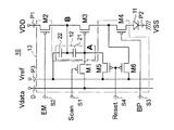
図1Aは実施形態1の画素回路の構成を示す回路図であり、図1Bは実施形態1の画素回路の動作を示すタイミング図である。以下、この図面に基づき説明する。
<
FIG. 1A is a circuit diagram illustrating a configuration of a pixel circuit according to the first embodiment, and FIG. 1B is a timing diagram illustrating an operation of the pixel circuit according to the first embodiment. Hereinafter, description will be given based on this drawing.
本実施形態1の画素回路10は、発光素子11と、印加された電圧に応じた電流を発光素子11へ供給する駆動トランジスタ(M3)と、駆動トランジスタ(M3)の閾値電圧Vth及びデータ電圧Vdataを含む電圧を保持し、この電圧を駆動トランジスタ(M3)に印加するコンデンサ部12と、閾値電圧Vth及びデータ電圧Vdataを含む電圧をコンデンサ部12に保持させるスイッチ部13と、を備えている。そして、スイッチ部13は、駆動トランジスタ(M3)から供給される電流を、発光素子11を通さずに基準電圧電源線(P3)へ迂回させる電流迂回用トランジスタ(M6)を有する。
The
また、スイッチ部13は、閾値電圧Vth及びデータ電圧Vdataを含む電圧をコンデンサ部12に保持させる前に、駆動トランジスタ(M3)及び電流迂回用トランジスタ(M6)をオンにする。
The
更に、スイッチ部13は、基準電圧電源線(P3)から基準電圧(Vref)を入力する基準電圧用トランジスタ(M5)と、データ線Dからデータ電圧Vdataを入力するデータ電圧用トランジスタ(M1)とを有する。
Further, the
より詳しく説明すると、駆動トランジスタ(M3)は、ゲート端子、ソース端子及びドレイン端子を有し、これらのゲート端子とソース端子との間に印加された電圧に応じた電流を、ドレイン端子に接続された発光素子11へ供給する。コンデンサ部12は、閾値電圧Vth及びデータ電圧Vdataを含む電圧を保持し、この電圧を駆動トランジスタ(M3)のゲート端子とソース端子との間に印加する。スイッチ部13は、電流迂回用トランジスタ(M6)、基準電圧用トランジスタ(M5)及びデータ電圧用トランジスタ(M1)を含む複数のトランジスタを有し、これらのトランジスタのスイッチング動作によって、コンデンサ部12に、閾値電圧Vthを含む電圧を保持させ、その後に閾値電圧Vth及びデータ電圧Vdataを含む電圧を保持させる。かつ、スイッチ部13は、閾値電圧Vthを含む電圧をコンデンサ部12に保持させる際に、電流迂回用トランジスタ(M6)及び基準電圧用トランジスタ(M5)をオンかつデータ電圧用トランジスタ(M1)をオフにすることにより、基準電圧Vrefをコンデンサ部12へ供給し、閾値電圧Vth及びデータ電圧Vdataを含む電圧をコンデンサ部12に保持させる際に、電流迂回用トランジスタ(M6)及び基準電圧用トランジスタ(M5)をオフかつデータ電圧用トランジスタ(M1)をオンにすることにより、データ電圧Vdataをコンデンサ部12へ供給する。
More specifically, the driving transistor (M3) has a gate terminal, a source terminal, and a drain terminal, and a current corresponding to a voltage applied between the gate terminal and the source terminal is connected to the drain terminal. The
本実施形態1の画素回路10によれば、駆動トランジスタ(M3)から供給される電流を発光素子11を通さずに基準電圧電源線(P3)へ迂回させる電流迂回用トランジスタ(M6)を有するので、リセット動作時に電流迂回用トランジスタ(M6)をオンにすることにより、リセット動作時の漏れ発光によるコントラスト低下を防止できる。
The
また、画素回路10によれば、閾値電圧Vth及びデータ電圧Vdataを含む電圧をコンデンサ部12に保持させる前に、駆動トランジスタ(M3)及び電流迂回用トランジスタ(M6)をオンにすることにより、発光素子11へ電流を供給する前に確実に駆動トランジスタ(M3)に電流を流すことができるので、駆動トランジスタ(M3)のヒステリシス特性の初期化を防ぐことができ、コントラスト低下を招くことなくイメージリテンションを防止できる。
Further, according to the
更に、画素回路10によれば、データ線Dからデータ電圧Vdataを入力するデータ電圧用トランジスタ(M1)とは別に、基準電圧電源線(P3)から基準電圧(Vref)を入力する基準電圧用トランジスタ(M5)を設けたことにより、データ線Dから供給される基準電圧(Vref)を用いずに閾値電圧Vthを検出できる。したがって、閾値電圧Vthの検出時に原理的にクロストークが発生しないことにより、高精細化が進んでも閾値電圧検出期間を十分に設定できるので、閾値電圧Vthの検出精度を向上できる。
Further, according to the
また、スイッチ部13は、閾値電圧Vthを含む電圧をコンデンサ部12に保持させる際に、1水平走査期間以上の時間にわたって電流迂回用トランジスタ(M6)及び基準電圧用トランジスタ(M5)をオンかつデータ電圧用トランジスタ(M1)をオフにすることにより、基準電圧(Vref)をコンデンサ部12へ供給するようにしてもよい。この場合は、閾値電圧検出期間をより十分に設定できるので、閾値電圧Vthの検出精度をより向上できる。なお、1水平走査期間内でできるだけ長く、電流迂回用トランジスタ(M6)及び基準電圧用トランジスタ(M5)をオンかつデータ電圧用トランジスタ(M1)をオフにするようにしてもよい。
In addition, when the
更に、スイッチ部13は、閾値電圧Vthを含む電圧をコンデンサ部12に保持させる際に、電流迂回用トランジスタ(M6)をオンにするとともに基準電圧(Vref)をコンデンサ部12へ供給することにより、駆動トランジスタ(M3)を一時的にオンにするようにしてもよい。この場合は、閾値電圧Vthの検出時に駆動トランジスタ(M3)に流れる微小な電流を、電流迂回用トランジスタ(M6)を介して発光素子11には流さずに基準電圧電源線(P3)へ流すことにより、漏れ発光によるコントラスト低下を防止できる。
Furthermore, the
次に、画素回路10について更に詳しく説明する。
Next, the
画素回路10は、データ線D、第1乃至第4制御線S1〜S4及び第1乃至第3電源線P1〜P3に電気的に接続され、第1乃至第6トランジスタM1〜M6、第1乃至第2コンデンサ21,22及び発光素子11を備えている。第3電源線P3が前述の基準電圧電源線(P3)に相当し、第1、第2、第4、第5及び第6トランジスタM1,M2,M4,M5,M6が前述のスイッチ部13を構成し、第1トランジスタM1が前述のデータ電圧用トランジスタ(M1)に相当し、第5トランジスタM5が前述の基準電圧用トランジスタ(M5)に相当し、第6トランジスタM6が前述の電流迂回用トランジスタ(M6)に相当し、第3トランジスタM3が前述の駆動トランジスタ(M3)に相当し、第1及び第2コンデンサ21,22が前述のコンデンサ部12を構成している。
The
第1トランジスタM1は、データ線Dに電気的に接続された第1端子と、第2端子と、第1制御線S1に電気的に接続された制御端子とを有する。第2トランジスタM2は、第1電源線P1に電気的に接続された第1端子と、第2端子と、第2制御線S2に電気的に接続された制御端子とを有する。 The first transistor M1 has a first terminal electrically connected to the data line D, a second terminal, and a control terminal electrically connected to the first control line S1. The second transistor M2 has a first terminal electrically connected to the first power supply line P1, a second terminal, and a control terminal electrically connected to the second control line S2.
第3トランジスタM3は、第2トランジスタM2の第2端子に電気的に接続されるとともに前述の駆動トランジスタ(M3)のソース端子に相当する第1端子と、前述の駆動トランジスタ(M3)のドレイン端子に相当する第2端子と、第1トランジスタM1の第2端子に電気的に接続されるとともに前述の駆動トランジスタ(M3)のゲート端子に相当する制御端子とを有する。 The third transistor M3 is electrically connected to the second terminal of the second transistor M2, and has a first terminal corresponding to the source terminal of the driving transistor (M3) and a drain terminal of the driving transistor (M3). And a control terminal that is electrically connected to the second terminal of the first transistor M1 and that corresponds to the gate terminal of the driving transistor (M3).
第4トランジスタM4は、第3トランジスタM3の第2端子に電気的に接続された第1端子と、第2端子と、第3制御線S3に電気的に接続された制御端子とを有する。 The fourth transistor M4 has a first terminal electrically connected to the second terminal of the third transistor M3, a second terminal, and a control terminal electrically connected to the third control line S3.
第5トランジスタM5は、第3電源線P3に電気的に接続された第1端子と、第1トランジスタM1の第2端子に電気的に接続された第2端子と、第4制御線S4に電気的に接続された制御端子とを有する。 The fifth transistor M5 is electrically connected to the first terminal electrically connected to the third power supply line P3, the second terminal electrically connected to the second terminal of the first transistor M1, and the fourth control line S4. Connected control terminals.
第6トランジスタM6は、第3電源線P3に電気的に接続された第1端子と、第3トランジスタM3の第2端子に電気的に接続された第2端子と、第4制御線S4に電気的に接続された制御端子とを有する。 The sixth transistor M6 is electrically connected to the first terminal electrically connected to the third power supply line P3, the second terminal electrically connected to the second terminal of the third transistor M3, and the fourth control line S4. Connected control terminals.
第1コンデンサ21は、第1トランジスタM1の第2端子に電気的に接続された第1端子と、第3トランジスタM3の第1端子に電気的に接続された第2端子とを有する。
The
第2コンデンサ22は、第3電源線P3に接続された第1端子と、第3トランジスタM3の第1端子に電気的に接続された第2端子とを有する。
The
発光素子11は、第4トランジスタM4の第2端子に電気的に接続された第1端子と、第2電源線P2に電気的に接続された第2端子とを有する。
The
ここで、第1制御線S1は第1制御信号Scanを出力し、第2制御線S2は第2制御信号EMを出力し、第3制御線S3は第3制御信号BPを出力し、第4制御線S4は第4制御信号Resetを出力する。各トランジスタにおいて、第1端子は例えばソース端子及びドレイン端子の一方であり、第2端子は例えばソース端子及びドレイン端子の他方であり、制御端子は例えばゲート端子である。発光素子11の第1端子はアノード端子及びカソード端子の一方(例えば本実施形態1ではアノード端子)であり、発光素子11の第2端子はアノード端子及びカソード端子の他方(例えば本実施形態1ではカソード端子)である。
Here, the first control line S1 outputs the first control signal Scan, the second control line S2 outputs the second control signal EM, the third control line S3 outputs the third control signal BP, and the fourth The control line S4 outputs a fourth control signal Reset. In each transistor, the first terminal is, for example, one of a source terminal and a drain terminal, the second terminal is, for example, the other of the source terminal and the drain terminal, and the control terminal is, for example, a gate terminal. The first terminal of the
また、第1トランジスタM1は、データ線Dから供給されるデータ電圧Vdataを、第1コンデンサ21の第1端子へ選択的に供給するように構成されている。第2トランジスタM2は、第1電源線P1から供給される第1電源電圧VDDを、第3トランジスタM3の第1端子、第1コンデンサ21の第2端子及び第2コンデンサ22の第2端子へ選択的に供給するように構成されている。第3トランジスタM3は、第1コンデンサ21の第2端子及び第2コンデンサ22の第2端子を第4トランジスタM4の第1端子に選択的に接続するように構成されている。第4トランジスタM4は、第3トランジスタM3の第2端子を発光素子11の第1端子に選択的に接続するように構成されている。第5トランジスタM5は、第3電源線P3から供給されるとともに前述の基準電圧(Vref)に相当する第3電源電圧Vrefを、第1コンデンサ21の第1端子へ選択的に供給するように構成されている。第6トランジスタM6は、第3電源線P3から供給される第3電源電圧Vrefを、第3トランジスタM3の第2端子へ選択的に供給するように構成されている。なお、第2電源線P2は、例えば接地電位である第2電源電圧VSSを、発光素子11の第2端子へ供給する。
The first transistor M1 is configured to selectively supply the data voltage Vdata supplied from the data line D to the first terminal of the
第1乃至第6トランジスタM1〜M6は、pチャネル型トランジスタであり、詳しくはpチャネル型TFTである。発光素子11はOLEDである。OLEDは一般に基板側(VSS側)がカソードになるので、そのアノードを駆動トランジスタのドレインに接続するには、駆動トランジスタをpチャネル型にする必要がある。そうすれば、OLEDの抵抗値が時間経過によって変化しても、OLEDに常に一定電流を供給できる。
The first to sixth transistors M1 to M6 are p-channel transistors, and more specifically, p-channel TFTs. The
スイッチ部13を構成する第1、第2、第4、第5及び第6トランジスタM1,M2,M4,M5,M6は、線形領域で動作するスイッチ用トランジスタである。第3トランジスタM3は、飽和領域で動作する増幅用トランジスタである。
The first, second, fourth, fifth, and sixth transistors M1, M2, M4, M5, and M6 constituting the
図2は、実施形態1の画素回路を備えた表示装置を示す平面図である。以下、この図面に基づき説明する。 FIG. 2 is a plan view illustrating a display device including the pixel circuit according to the first embodiment. Hereinafter, description will be given based on this drawing.
本実施形態1における表示装置30はAMOLEDである。表示装置30は、大別して、発光素子を含む複数の画素回路(図1A参照)がマトリクス状に配置されたTFT基板100と、発光素子を封止する封止ガラス基板200と、TFT基板100と封止ガラス基板200とを接合するガラスフリットシール部300などで構成される。また、TFT基板100のアクティブマトリクス部116の外側のカソード電極形成領域114aの周囲には、TFT基板100の走査線(各制御線)を駆動する走査ドライバ131、各画素の発光期間を制御するエミッション制御ドライバ132、静電気放電による破損を防ぐデータ線ESD(Electro-Static-Discharge)保護回路133、高転送レートのストリームを本来の低転送レートの複数のストリームに戻すデマルチプレクサ134、データ線を駆動するデータドライバIC135などが配置されている。データドライバIC135は、異方性導電フィルムを用いてTFT基板100に実装される。TFT基板100は、FPC(Flexible Printed Circuit)136を介して外部の機器と接続される。なお、図2は、本実施形態1における表示装置の一例であり、その形状や構成は適宜変更可能である。
The
図1Aと図2との対応関係は次のとおりである。図1Aにおける第1制御線S1及び第4制御線S4は、図2における走査ドライバ131に接続されている。図1Aにおける第2制御線S2及び第3制御線S3は、図2におけるエミッション制御ドライバ132に接続されている。図1Aにおけるデータ線Dは、図2におけるデマルチプレクサ134及びデータドライバIC135に接続されている。図1Aにおける第1乃至第3電源線P1〜P3は、図2におけるFPC136を介して外部の電源と接続されている。
The correspondence between FIG. 1A and FIG. 2 is as follows. The first control line S1 and the fourth control line S4 in FIG. 1A are connected to the
図3は、図2の一部を拡大して示す断面図である。以下、この図面に基づき説明する。 FIG. 3 is an enlarged cross-sectional view of a part of FIG. Hereinafter, description will be given based on this drawing.
TFT基板100は、ガラス基板101上に下地絶縁膜102を介して形成された低温ポリシリコン(LTPS:Low Temperature Polycrystalline Silicon)等からなるポリシリコン層103と、ゲート絶縁膜104を介して形成された第1金属層105(ゲート電極及びコンデンサ電極)と、層間絶縁膜106に形成された開口を介してポリシリコン層103に接続される第2金属層107(データ線、電源線、ソース及びドレイン電極、コンタクト部)と、平坦化膜110を介して素子分離膜112の凹部に形成される発光素子11(アノード電極111、有機EL層113、カソード電極114及びキャップ層115)とから構成される。
The
TFT領域108におけるポリシリコン層103は、LDD(Lightly Doped Drain)構造になっており、左からp+層、p−層、i層、p−層、p+層である。コンデンサ領域109におけるポリシリコン層103はp+層である。
The
発光素子11と封止ガラス基板200との間には乾燥空気301が封入され、これらがガラスフリットシール部300(図2)によって封止されることにより、表示装置30が形成される。この発光素子11はトップエミッション構造であり、発光素子11と封止ガラス基板200とは所定の間隔に設定されるとともに、封止ガラス基板200の光出射面側にλ/4位相差板201と偏光板202とが形成され、外部から入射した光の反射が抑制されるようになっている。
なお、図3では、発光素子11の各放射光が、封止ガラス基板200を介して外部に放射されるトップエミッション構造を示したが、ガラス基板101を介して外部に放射されるボトムエミッション構造とすることもできる。
3 shows a top emission structure in which each radiated light of the
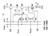
図4A乃至図7Bは本実施形態1の画素回路の動作(駆動方法)を示し、図4A、図5A、図6A及び図7Aは第1乃至第4期間における回路図であり、図4B、図5B、図6B及び図7Bは第1乃至第4期間におけるタイミング図である。以下、図1A及びに図1Bに図4A乃至図7Bを加えて、本実施形態1の画素回路の動作(駆動方法)について説明する。
4A to 7B show the operation (driving method) of the pixel circuit of
なお、図4A、図5A、図6A及び図7Aでは、見やすくするために、図1Aで付した符号の一部を省略している。図4A、図5A、図6A及び図7A中の「×」印は、オフ状態のトランジスタを示す。画素回路の駆動方法によって画素回路が動作するので、画素回路の動作(駆動方法)と表記している。 4A, FIG. 5A, FIG. 6A, and FIG. 7A, a part of the reference numerals attached in FIG. 1A is omitted for easy understanding. In FIG. 4A, FIG. 5A, FIG. 6A, and FIG. 7A, “x” marks indicate transistors that are off. Since the pixel circuit operates according to the driving method of the pixel circuit, the operation (driving method) of the pixel circuit is described.
まず、図1A及び図1Bに基づき、画素回路10の駆動方法の概要を説明する。画素回路10の駆動方法は、次の第1乃至第4期間T1〜T4を含む。このとき、スイッチ部13は、次のように動作する。
First, an outline of a driving method of the
第1期間T1に、コンデンサ部12に保持された電圧を初期化する。
第1期間T1の後の第2期間T2に、電流迂回用トランジスタ(M6)及び基準電圧用トランジスタ(M5)をオンにして駆動トランジスタ(M1)の閾値電圧Vthを含む電圧をコンデンサ部12に保持させる。
第2期間T2の後の第3期間T3に、データ電圧用トランジスタ(M1)をオンにして、データ電圧Vdataをコンデンサ部12に供給して、閾値電圧Vth及びデータ電圧Vdataを含む電圧をコンデンサ部12に保持させる。
第3期間T3の後の第4期間T4に、駆動トランジスタ(M3)にコンデンサ部12で保持された電圧を印加することにより、データ電圧Vdataに応じた電流を発光素子11へ供給する。
In the first period T1, the voltage held in the
In the second period T2 after the first period T1, the current bypassing transistor (M6) and the reference voltage transistor (M5) are turned on to hold the voltage including the threshold voltage Vth of the driving transistor (M1) in the
In the third period T3 after the second period T2, the data voltage transistor (M1) is turned on, the data voltage Vdata is supplied to the
In a fourth period T4 after the third period T3, a voltage corresponding to the data voltage Vdata is supplied to the
より詳しく言えば、第1期間T1に、コンデンサ部12に保持された電圧を初期化する。
第2期間T2に、電流迂回用トランジスタ(M6)及び基準電圧用トランジスタ(M5)をオンかつデータ電圧用トランジスタ(M1)をオフにすることにより、駆動トランジスタ(M3)の閾値電圧Vthを含む電圧をコンデンサ部12に保持させる。
第3期間T3に、電流迂回用トランジスタ(M6)及び基準電圧用トランジスタ(M5)をオフかつデータ電圧用トランジスタ(M1)をオンにすることにより、データ電圧Vdataをコンデンサ部12に供給して、閾値電圧Vth及びデータ電圧Vdataを含む電圧をコンデンサ部12に保持させる。
第4期間T4に、駆動トランジスタ(M3)のゲート端子とソース端子との間にコンデンサ部12で保持された電圧を印加することにより、データ電圧Vdataに応じた電流を発光素子11へ供給する。
More specifically, the voltage held in the
In the second period T2, the voltage including the threshold voltage Vth of the drive transistor (M3) is turned on by turning on the current bypass transistor (M6) and the reference voltage transistor (M5) and turning off the data voltage transistor (M1). Is held by the
In the third period T3, by turning off the current bypass transistor (M6) and the reference voltage transistor (M5) and turning on the data voltage transistor (M1), the data voltage Vdata is supplied to the
In the fourth period T4, a voltage corresponding to the data voltage Vdata is supplied to the
また、第1期間T1に、コンデンサ部12に保持された電圧を初期化するとともに、駆動トランジスタ(M3)及び電流迂回用トランジスタ(M6)をオンにして、駆動トランジスタ(M3)に電流を流し、その電流を電流迂回用トランジスタ(M6)を介して発光素子11へ流さずに基準電圧電源線(P3)へ流すようにしてもよい。
Further, in the first period T1, the voltage held in the
次に、各期間ごとに詳しく説明する。 Next, each period will be described in detail.
図4A及び図4Bに示す第1期間T1では、第1トランジスタM1及び第4トランジスタM4をオフにし、第2トランジスタM2、第3トランジスタM3、第5トランジスタM5及び第6トランジスタM6をオンにするように第1乃至第4制御線S1〜S4の電圧を設定する。 In the first period T1 shown in FIGS. 4A and 4B, the first transistor M1 and the fourth transistor M4 are turned off, and the second transistor M2, the third transistor M3, the fifth transistor M5, and the sixth transistor M6 are turned on. The voltages of the first to fourth control lines S1 to S4 are set.
このとき、このとき、ノードAの電圧VAは第5トランジスタM5を介して第3電源電圧Vrefとなり、ノードBの電圧VBは第2トランジスタM2を介して第1電源電圧VDDとなる。つまり、ノードAの電圧VA及びノードBの電圧VBは次式のようになり、第1及び第2コンデンサ21,22に保持された電圧が初期化される。
VA=Vref
VB=VDD
At this time, the voltage VA at the node A becomes the third power supply voltage Vref via the fifth transistor M5, and the voltage VB at the node B becomes the first power supply voltage VDD via the second transistor M2. That is, the voltage VA at the node A and the voltage VB at the node B are expressed by the following equations, and the voltages held in the first and
VA = Vref
VB = VDD
一方、第3トランジスタM3及び第6トランジスタM6がオンになることにより、第3トランジスタM3に電流i1が流れ、その電流i1が第6トランジスタM6を介して発光素子11へ流れずに第3電源線P3へ流れる。
On the other hand, when the third transistor M3 and the sixth transistor M6 are turned on, the current i1 flows to the third transistor M3, and the current i1 does not flow to the
このとき、第3トランジスタM3のゲート端子とソース端子との間に印加される電圧はVB−VAであるから、そのドレイン端子に流れる電流i1は次式で与えられる。
i1=1/2β((VB−VA)−Vth)2
=1/2β(VDD−Vref−Vth)2
At this time, since the voltage applied between the gate terminal and the source terminal of the third transistor M3 is VB-VA, the current i1 flowing through the drain terminal is given by the following equation.
i1 = 1 / 2β ((VB−VA) −Vth) 2
= 1 / 2β (VDD−Vref−Vth) 2
上式からわかるように、電流i1は白表示レベル程度の十分に大きな値であるので、第3トランジスタM3のヒステリシス特性の初期化が防止される。これが、画素回路10のイメージリテンション防止機能である。なお、上式中のβは、第3トランジスタM3の構造及び材質によって決まる定数である。
As can be seen from the above equation, since the current i1 is a sufficiently large value on the order of the white display level, initialization of the hysteresis characteristics of the third transistor M3 is prevented. This is the image retention prevention function of the
図5A及び図5Bに示す第2期間T2では、第1トランジスタM1及び第2トランジスタM2をオフにし、第3トランジスタM3、第4トランジスタM4、第5トランジスタM5及び第6トランジスタM6をオンにするように第1乃至第4制御線S1〜S4の電圧を設定する。 In the second period T2 shown in FIGS. 5A and 5B, the first transistor M1 and the second transistor M2 are turned off, and the third transistor M3, the fourth transistor M4, the fifth transistor M5, and the sixth transistor M6 are turned on. The voltages of the first to fourth control lines S1 to S4 are set.
このとき、ノードAの電圧VAは第5トランジスタM5を介して第3電源電圧Vrefとなる。そのため、第1及び第2コンデンサ21,22に保持された電荷が第3トランジスタM3及び第6トランジスタM6を介して放電されることにより、第3トランジスタM3から電流i2が流れるので、ノードBの電圧VBは第1電源電圧VDDから低下する。ノードBの電圧VBが低下してVref+Vthになると、第3トランジスタM3がオフとなる。つまり、ノードAの電圧VA及びノードBの電圧VBは次式のようになり、第3トランジスタM3の閾値電圧Vthを含む電圧が第1及び第2コンデンサ21,22に保持される。このように、本実施形態1では、ソースフォロア型の閾値電圧検出を用いている。
VA=Vref
VB=Vref+Vth
At this time, the voltage VA of the node A becomes the third power supply voltage Vref via the fifth transistor M5. Therefore, since the electric charge held in the first and
VA = Vref
VB = Vref + Vth
閾値電圧検出に必要な基準電圧である第3電源電圧Vrefは、第5トランジスタM5を介してデータ線Dとは別の第3電源線P3から供給される。したがって、閾値電圧検出中は、データ線Dの影響を受けないので、原理的にクロストークを生じない。そのため、N(自然数)×H(水平走査期間)分の時間で閾値電圧Vthを検出できる。よって、十分な時間で閾値電圧Vthを検出できることにより、正確な閾値電圧Vthが得られるので、閾値電圧Vthの補償性能が高い。なお、本実施形態1はN=2の場合である。 The third power supply voltage Vref, which is a reference voltage necessary for threshold voltage detection, is supplied from a third power supply line P3 different from the data line D through the fifth transistor M5. Therefore, since the threshold voltage is not affected by the data line D, in principle, no crosstalk occurs. Therefore, the threshold voltage Vth can be detected in a time corresponding to N (natural number) × H (horizontal scanning period). Therefore, since the threshold voltage Vth can be detected in a sufficient time, an accurate threshold voltage Vth can be obtained, so that the compensation performance of the threshold voltage Vth is high. In the first embodiment, N = 2.
また、閾値電圧検出時に駆動トランジスタである第3トランジスタM3が一時的にオンになることによって流れる電流i2は、第6トランジスタM6を介して発光素子11へ流れずに第3電源線P3へ流れる。そのため、閾値電圧検出時に発光素子11へ電流が供給されないので、漏れ発光によるコントラスト低下を防止できる。これが、画素回路10のコントラスト低下防止機能である。
Further, the current i2 that flows when the third transistor M3, which is a driving transistor, is temporarily turned on when the threshold voltage is detected does not flow to the
図6A及び図6Bに示す第3期間T3では、第2トランジスタM2、第4トランジスタM4、第5トランジスタM5及び第6トランジスタM6をオフにし、第1トランジスタM1及び第3トランジスタM3をオンにするように第1乃至第4制御線S1〜S4の電圧を設定し、かつ、データ線Dからデータ電圧Vdataを供給する。 In the third period T3 shown in FIGS. 6A and 6B, the second transistor M2, the fourth transistor M4, the fifth transistor M5, and the sixth transistor M6 are turned off, and the first transistor M1 and the third transistor M3 are turned on. Are set to voltages of the first to fourth control lines S1 to S4, and a data voltage Vdata is supplied from the data line D.
このとき、ノードAの電圧VAは第1トランジスタM1を介してデータ電圧Vdataとなる。一方、第1及び第2コンデンサ21,22の容量値をそれぞれC1,C2とすると、ノードBの電圧VBは、直列接続された第1及び第2コンデンサ21,22の分圧であるK(Vdata−Vref)だけ上昇して次式のようになる。つまり、データ電圧Vdataを第1及び第2コンデンサ21,22に供給することにより、閾値電圧Vth及びデータ電圧Vdataを含む電圧を第1及び第2コンデンサ21,22に保持させる。
VA=Vdata
VB=Vref+Vth+K(Vdata−Vref)
K=C1/(C1+C2)
ここで、C1<C2すなわちK<1/2とする。その理由は、後述する式からわかるように、第3トランジスタM3に印加されるVdataの項を大きくするためである。
At this time, the voltage VA of the node A becomes the data voltage Vdata through the first transistor M1. On the other hand, assuming that the capacitance values of the first and
VA = Vdata
VB = Vref + Vth + K (Vdata−Vref)
K = C1 / (C1 + C2)
Here, C1 <C2, that is, K <1/2. The reason for this is to increase the term of Vdata applied to the third transistor M3, as can be seen from the equation described later.
図7A及び図7Bに示す第4期間T4では、第1トランジスタM1、第5トランジスタM5及び第6トランジスタM6をオフにし、第2トランジスタM2、第3トランジスタM3及び第4トランジスタM4をオンにするように第1乃至第4制御線S1〜S4の電圧を設定する。 In the fourth period T4 shown in FIGS. 7A and 7B, the first transistor M1, the fifth transistor M5, and the sixth transistor M6 are turned off, and the second transistor M2, the third transistor M3, and the fourth transistor M4 are turned on. The voltages of the first to fourth control lines S1 to S4 are set.
このとき、ノードBの電圧VBは第2トランジスタM2を介して第1電源電圧VDDとなる。一方、ノードAの電圧VAは、第1電源電圧VDDから第3期間T3での電圧VBを引いた分が、第3期間T3での電圧VAに加わって次式のようになる。
VA=Vdata+(VDD−Vref−Vth−K(Vdata−Vref))
=(1−K)Vdata+(K−1)Vref−Vth+VDD
VB=VDD
At this time, the voltage VB at the node B becomes the first power supply voltage VDD via the second transistor M2. On the other hand, the voltage VA at the node A is obtained by subtracting the voltage VB in the third period T3 from the first power supply voltage VDD and adding it to the voltage VA in the third period T3 as follows.
VA = Vdata + (VDD−Vref−Vth−K (Vdata−Vref))
= (1-K) Vdata + (K-1) Vref-Vth + VDD
VB = VDD
これにより、第3トランジスタM3のゲート端子とソース端子との間に印加される電圧はVB−VAであるから、そのドレイン端子に流れる電流Iは次式で与えられる。
I=1/2β((VB−VA)−Vth)2
=1/2β(VDD−((1−K)Vdata+(K−1)Vref−Vth+VDD)−Vth)2
=1/2β((1−K)Vref−(1−K)Vdata)2
Thus, since the voltage applied between the gate terminal and the source terminal of the third transistor M3 is VB-VA, the current I flowing through the drain terminal is given by the following equation.
I = 1 / 2β ((VB−VA) −Vth) 2
= 1 / 2β (VDD − ((1−K) Vdata + (K−1) Vref−Vth + VDD) −Vth) 2
= 1 / 2β ((1-K) Vref− (1-K) Vdata) 2
上式からわかるように、電流Iは、閾値電圧Vthの項を含まないので、閾値電圧Vthのバラツキ及び変動の影響を受けない。これが、画素回路10の閾値電圧Vthバラツキ補償機能である。
As can be seen from the above equation, the current I does not include the term of the threshold voltage Vth, and therefore is not affected by variations and fluctuations in the threshold voltage Vth. This is the threshold voltage Vth variation compensation function of the
以上のように、第4期間T4では、第3トランジスタM3のゲート端子とソース端子との間に第1及び第2コンデンサ21,22で保持された電圧を印加することにより、データ電圧Vdataに応じた電流Iを発光素子11へ供給する。
As described above, in the fourth period T4, the voltage held by the first and
なお、VDD>Vref>VSSが成り立ち、例えばVDD=10V、VSS=0V、Vref=7〜8V、Vdata=1〜6Vである。 Note that VDD> Vref> VSS is established, and for example, VDD = 10V, VSS = 0V, Vref = 7 to 8V, and Vdata = 1 to 6V.
換言すると、本実施形態1の効果は次のとおりである。1)リセット時に流れる電流をバイパスさせてOLEDへ流さないため、原理的にコントラストが低下しない。2)OLED駆動用のトランジスタに、OLEDを駆動する度に電流を流すことにより、イメージリテンションの問題を生じない。3)閾値電圧検出期間を独立に制御できる回路になっているため、閾値電圧を十分に長い時間をとって精度良く検出できる。したがって、表示ムラの補償能力が高く、より均一な表示特性が得られる。4)閾値電圧検出期間中にデータ信号の変化の影響を受けないため、原理的にクロストークを生じない。5)以上のように、コントラスト低下やイメージリテンションが発生せず、閾値電圧のバラツキや変動に対する補償能力が高く、しかもクロストークも生じないので、高画質化を実現できる。また、後述するようにデマルチプレクサの適用も容易であるため、データドライバICの出力ピン数も減らすことができて実用的である。 In other words, the effects of the first embodiment are as follows. 1) Since the current flowing at the time of reset is bypassed and does not flow to the OLED, the contrast is not lowered in principle. 2) By causing a current to flow through the OLED driving transistor each time the OLED is driven, the problem of image retention does not occur. 3) Since the circuit can control the threshold voltage detection period independently, the threshold voltage can be detected accurately with a sufficiently long time. Therefore, the display unevenness compensation capability is high, and more uniform display characteristics can be obtained. 4) Since it is not affected by the change of the data signal during the threshold voltage detection period, in principle, no crosstalk occurs. 5) As described above, contrast reduction and image retention do not occur, compensation capability for variations and fluctuations in threshold voltage is high, and crosstalk does not occur, so that high image quality can be realized. Further, as will be described later, since the demultiplexer can be easily applied, the number of output pins of the data driver IC can be reduced, which is practical.
<実施形態2>
図8Aは実施形態2の表示装置の一部を示す回路図であり、図8Bは実施形態3の表示装置の動作を示すタイミング図である。以下、これらの図面に基づき説明する。
<
FIG. 8A is a circuit diagram illustrating a part of the display device according to the second embodiment, and FIG. 8B is a timing diagram illustrating an operation of the display device according to the third embodiment. Hereinafter, description will be given based on these drawings.
本実施形態2の表示装置は、デマルチプレクサ134に特徴を有する。図8Aに示すデマルチプレクサ134は1画素分である。実施形態1の画素回路をサブ画素とした場合、RGBの三つのサブ画素から1画素が構成される。各画素回路は、例えばRGB縦ストライプ方式の配列構造になっている。
The display device according to the second embodiment is characterized by a
デマルチプレクサ134は、三つの画素回路にそれぞれ接続する三本のデータ線Dnr,Dng,Dnbの中から一本のデータ線を順次選択し、選択された一本のデータ線をデータ電圧Vdataの供給源(図2に示すデータドライバIC135)に接続された他の一本のデータ線Dnに接続する。データ線Dnr,Dng,Dnbは、それぞれ図1Aにおけるデータ線Dに相当する。
The
デマルチプレクサ134は、1画素につき三つのスイッチ用のトランジスタMnr、Mng,Mnbを有する。トランジスタMnr、Mng,Mnbはそれぞれ、第5制御信号R_set,G_set,G_setによって、三本のデータ線Dnr,Dng,Dnbを選択的に一本のデータ線Dnに接続する。データ線Dnからは、トランジスタMnrを介してデータ線Dnrへデータ電圧Rnが出力され、トランジスタMngを介してデータ線Dngへデータ電圧Rgが出力され、トランジスタMnbを介してデータ線Dnbへデータ電圧Rbが出力される。
The
第5制御信号R_set,G_set,G_setは、互いに重ならないように時間をずらして1水平走査期間1H内に出力される。全てのデータ線Dnr,Dng,Dnbのデータ電圧Rr,Rg,Rbが確定してから、トランジスタM1(図1A)をオンにする。デマルチプレクサ134を用いることにより、データドライバIC135(図2)のデータ線Dの総数を削減できる。
The fifth control signals R_set, G_set, and G_set are output within one
一本のデータ線から出力されたデータ電圧を三本のデータ線へ分けるデマルチプレクサを用いた既存の画素回路では、閾値電圧検出及びデータ書き込みの両方を1水平走査期間内にする必要があった。ところが、高精細化に伴う走査線数の増加により、1水平走査期間が短くなると、データ線一本当たりの書き込み時間が短くなってデータ書き込みが不十分となる。 In an existing pixel circuit using a demultiplexer that divides a data voltage output from one data line into three data lines, both threshold voltage detection and data writing must be within one horizontal scanning period. . However, when the horizontal scanning period is shortened due to an increase in the number of scanning lines accompanying the increase in definition, the writing time per data line is shortened and data writing becomes insufficient.
これに対し、本実施形態2の表示装置では、実施形態1の画素回路を用いたことにより、1水平走査期間1Hのほぼ全体(第3期間T3)をデマルチプレクサ134によるデータ書き込みに利用できるので、第5制御信号R_set,G_set,G_setのパルス幅を十分にとることができ、これにより表示性能を向上できる。
On the other hand, in the display device according to the second embodiment, by using the pixel circuit according to the first embodiment, almost the entire one
本実施形態2のその他の構成、作用及び効果は、実施形態1のそれらと同様である。 Other configurations, operations, and effects of the second embodiment are the same as those of the first embodiment.
<総括>
以上、本発明を上記各実施形態に即して説明したが、本発明は、上記各実施形態の構成や動作にのみ限定されるものではなく、本発明の範囲内で当業者であればなし得ることが可能な各種変形及び修正を含むことはもちろんである。また、本発明には、上記各実施形態の構成の一部又は全部を相互に適宜組み合わせたものも含まれる。
<Summary>
As described above, the present invention has been described with reference to each of the above embodiments, but the present invention is not limited only to the configuration and operation of each of the above embodiments, and can be made by those skilled in the art within the scope of the present invention. Of course, it includes various variations and modifications that can be made. Further, the present invention includes a combination of some or all of the configurations of the above-described embodiments as appropriate.
例えば、各実施形態では全てのトランジスタをpチャネル型としたが、これに限らず、一部又は全部のトランジスタをnチャネル型としもよい。このとき、OLEDの駆動トランジスタをnチャネル型とした場合は、そのドレイン端子にOLEDのカソード端子が接続されるようにOLEDの導通方向を逆向きにする。トランジスタを構成する半導体材料は、LTPSなどのシリコンに限らず、IGZO(Indium Gallium Zinc Oxide)などの酸化物半導体を用いてもよい。また、スイッチ部は、ソースフォロワ型の閾値電圧検出構造としたが、ダイオード接続型の閾値電圧検出構造としてもよい。 For example, in the embodiments, all transistors are p-channel type, but this is not limiting, and some or all of the transistors may be n-channel type. At this time, when the driving transistor of the OLED is an n-channel type, the conduction direction of the OLED is reversed so that the cathode terminal of the OLED is connected to the drain terminal. The semiconductor material forming the transistor is not limited to silicon such as LTPS, and an oxide semiconductor such as IGZO (Indium Gallium Zinc Oxide) may be used. In addition, the switch unit has a source follower type threshold voltage detection structure, but may have a diode connection type threshold voltage detection structure.
上記の実施形態の一部又は全部は以下の付記のようにも記載され得るが、本発明は以下の構成に限定されるものではない。 Although a part or all of the above embodiments can be described as the following supplementary notes, the present invention is not limited to the following configurations.
[付記1]発光素子と、
印加された電圧に応じた電流を前記発光素子へ供給する駆動トランジスタと、
前記駆動トランジスタの閾値電圧及びデータ電圧を含む電圧を保持し、この電圧を前記駆動トランジスタに印加するコンデンサ部と、
前記閾値電圧及び前記データ電圧を含む電圧を前記コンデンサ部に保持させるスイッチ部と、
を備えた画素回路において、
前記スイッチ部は、前記駆動トランジスタから供給される電流を、前記発光素子を通さずに基準電圧電源線へ迂回させる電流迂回用トランジスタを有する、
ことを特徴とする画素回路。
[Appendix 1] a light emitting device;
A drive transistor for supplying a current corresponding to the applied voltage to the light emitting element;
A capacitor unit that holds a voltage including a threshold voltage and a data voltage of the driving transistor and applies the voltage to the driving transistor;
A switch unit that holds the voltage including the threshold voltage and the data voltage in the capacitor unit;
In a pixel circuit comprising:
The switch unit includes a current bypass transistor that bypasses the current supplied from the drive transistor to a reference voltage power line without passing through the light emitting element.
A pixel circuit characterized by that.
[付記2]付記1記載の画素回路において、
前記スイッチ部は、前記閾値電圧及び前記データ電圧を含む電圧を前記コンデンサ部に保持させる前に、前記駆動トランジスタ及び前記電流迂回用トランジスタをオンにする、
ことを特徴とする画素回路。
[Appendix 2] In the pixel circuit described in
The switch unit turns on the driving transistor and the current bypass transistor before holding the voltage including the threshold voltage and the data voltage in the capacitor unit.
A pixel circuit characterized by that.
[付記3]付記1又は2記載の画素回路において、
前記スイッチ部は、前記基準電圧電源線から基準電圧を入力する基準電圧用トランジスタと、データ線から前記データ電圧を入力するデータ電圧用トランジスタとを更に有する、
ことを特徴とする画素回路。
[Appendix 3] In the pixel circuit according to
The switch section further includes a reference voltage transistor for inputting a reference voltage from the reference voltage power supply line, and a data voltage transistor for inputting the data voltage from a data line.
A pixel circuit characterized by that.
[付記4]付記3記載の画素回路において、
前記駆動トランジスタは、ゲート端子、ソース端子及びドレイン端子を有し、これらのゲート端子とソース端子との間に印加された電圧に応じた電流を、前記ドレイン端子に接続された前記発光素子へ供給し、
前記コンデンサ部は、前記閾値電圧及び前記データ電圧を含む電圧を保持し、この電圧を前記駆動トランジスタの前記ゲート端子と前記ソース端子との間に印加し、
前記スイッチ部は、
前記電流迂回用トランジスタ、前記基準電圧用トランジスタ及び前記データ電圧用トランジスタを含む複数のトランジスタを有し、これらのトランジスタのスイッチング動作によって、前記コンデンサ部に、前記閾値電圧を含む電圧を保持させ、その後に前記閾値電圧及び前記データ電圧を含む電圧を保持させ、かつ、
前記閾値電圧を含む電圧を前記コンデンサ部に保持させる際に、前記電流迂回用トランジスタ及び前記基準電圧用トランジスタをオンかつ前記データ電圧用トランジスタをオフにすることにより、前記基準電圧を前記コンデンサ部へ供給し、
前記閾値電圧及び前記データ電圧を含む電圧を前記コンデンサ部に保持させる際に、前記電流迂回用トランジスタ及び前記基準電圧用トランジスタをオフかつ前記データ電圧用トランジスタをオンにすることにより、前記データ電圧を前記コンデンサ部へ供給する、
ことを特徴とする画素回路。
[Appendix 4] In the pixel circuit described in
The driving transistor has a gate terminal, a source terminal, and a drain terminal, and supplies a current corresponding to a voltage applied between the gate terminal and the source terminal to the light emitting element connected to the drain terminal. And
The capacitor unit holds a voltage including the threshold voltage and the data voltage, and applies this voltage between the gate terminal and the source terminal of the driving transistor,
The switch part is
A plurality of transistors including the current bypass transistor, the reference voltage transistor, and the data voltage transistor, and the switching operation of these transistors causes the capacitor unit to hold a voltage including the threshold voltage; Holding a voltage including the threshold voltage and the data voltage, and
When the voltage including the threshold voltage is held in the capacitor unit, the reference voltage is supplied to the capacitor unit by turning on the current bypass transistor and the reference voltage transistor and turning off the data voltage transistor. Supply
When holding the voltage including the threshold voltage and the data voltage in the capacitor unit, the data voltage is reduced by turning off the current bypass transistor and the reference voltage transistor and turning on the data voltage transistor. Supplying to the capacitor unit,
A pixel circuit characterized by that.
[付記5]付記4記載の画素回路において、
前記スイッチ部は、
前記閾値電圧を含む電圧を前記コンデンサ部に保持させる際に、1水平走査期間以上の時間にわたって前記電流迂回用トランジスタ及び前記基準電圧用トランジスタをオンかつ前記データ電圧用トランジスタをオフにすることにより、前記基準電圧を前記コンデンサ部へ供給する、
ことを特徴とする画素回路。
[Appendix 5] In the pixel circuit described in
The switch part is
When holding the voltage including the threshold voltage in the capacitor unit, by turning on the current bypass transistor and the reference voltage transistor and turning off the data voltage transistor over a time of one horizontal scanning period or more, Supplying the reference voltage to the capacitor unit;
A pixel circuit characterized by that.
[付記6]付記4又は5記載の画素回路において、
前記スイッチ部は、
前記閾値電圧を含む電圧を前記コンデンサ部に保持させる際に、前記電流迂回用トランジスタをオンにするとともに前記基準電圧を前記コンデンサ部へ供給することにより、前記駆動トランジスタを一時的にオンにする、
ことを特徴とする画素回路。
[Appendix 6] In the pixel circuit described in
The switch part is
When the voltage including the threshold voltage is held in the capacitor unit, the drive transistor is temporarily turned on by turning on the current bypass transistor and supplying the reference voltage to the capacitor unit.
A pixel circuit characterized by that.
[付記7]付記4乃至6のいずれか一つに記載の画素回路において、
前記データ線、第1乃至第4制御線及び第1乃至第3電源線に電気的に接続され、第1乃至第6トランジスタ、第1乃至第2コンデンサ及び前記発光素子を備え、
前記第3電源線が前記基準電圧電源線に相当し、前記第1、第2、第4、第5及び第6トランジスタが前記スイッチ部を構成し、前記第1トランジスタが前記データ電圧用トランジスタに相当し、前記第5トランジスタが前記基準電圧用トランジスタに相当し、前記第6トランジスタが前記電流迂回用トランジスタに相当し、前記第3トランジスタが前記駆動トランジスタに相当し、前記第1及び第2コンデンサが前記コンデンサ部を構成し、
前記第1トランジスタは、前記データ線に電気的に接続された第1端子と、第2端子と、前記第1制御線に電気的に接続された制御端子とを有し、
前記第2トランジスタは、前記第1電源線に電気的に接続された第1端子と、第2端子と、前記第2制御線に電気的に接続された制御端子とを有し、
前記第3トランジスタは、前記第2トランジスタの前記第2端子に電気的に接続されるとともに前記ソース端子に相当する第1端子と、前記ドレイン端子に相当する第2端子と、前記第1トランジスタの前記第2端子に電気的に接続されるとともに前記ゲート端子に相当する制御端子とを有し、
前記第4トランジスタは、前記第3トランジスタの前記第2端子に電気的に接続された第1端子と、第2端子と、前記第3制御線に電気的に接続された制御端子とを有し、
前記第5トランジスタは、前記第3電源線に電気的に接続された第1端子と、前記第1トランジスタの前記第2端子に電気的に接続された第2端子と、前記第4制御線に電気的に接続された制御端子とを有し、
前記第6トランジスタは、前記第3電源線に電気的に接続された第1端子と、前記第3トランジスタの前記第2端子に電気的に接続された第2端子と、前記第4制御線に電気的に接続された制御端子とを有し、
前記第1コンデンサは、前記第1トランジスタの前記第2端子に電気的に接続された第1端子と、前記第3トランジスタの前記第1端子に電気的に接続された第2端子とを有し、
前記第2コンデンサは、前記第3電源線に接続された第1端子と、前記第3トランジスタの前記第1端子に電気的に接続された第2端子とを有し、
前記発光素子は、前記第4トランジスタの前記第2端子に電気的に接続された第1端子と、前記第2電源線に電気的に接続された第2端子とを有する、
ことを特徴とする画素回路。
[Appendix 7] In the pixel circuit according to any one of
Electrically connected to the data line, the first to fourth control lines, and the first to third power lines, and includes first to sixth transistors, first to second capacitors, and the light emitting element;
The third power supply line corresponds to the reference voltage power supply line, the first, second, fourth, fifth and sixth transistors constitute the switch unit, and the first transistor serves as the data voltage transistor. The fifth transistor corresponds to the reference voltage transistor, the sixth transistor corresponds to the current bypass transistor, the third transistor corresponds to the drive transistor, and the first and second capacitors. Constitutes the capacitor part,
The first transistor has a first terminal electrically connected to the data line, a second terminal, and a control terminal electrically connected to the first control line,
The second transistor has a first terminal electrically connected to the first power supply line, a second terminal, and a control terminal electrically connected to the second control line,
The third transistor is electrically connected to the second terminal of the second transistor and has a first terminal corresponding to the source terminal, a second terminal corresponding to the drain terminal, and a first terminal of the first transistor. A control terminal electrically connected to the second terminal and corresponding to the gate terminal;
The fourth transistor has a first terminal electrically connected to the second terminal of the third transistor, a second terminal, and a control terminal electrically connected to the third control line. ,
The fifth transistor includes a first terminal electrically connected to the third power supply line, a second terminal electrically connected to the second terminal of the first transistor, and a fourth control line. A control terminal electrically connected,
The sixth transistor includes a first terminal electrically connected to the third power supply line, a second terminal electrically connected to the second terminal of the third transistor, and a fourth control line. A control terminal electrically connected,
The first capacitor has a first terminal electrically connected to the second terminal of the first transistor and a second terminal electrically connected to the first terminal of the third transistor. ,
The second capacitor has a first terminal connected to the third power supply line, and a second terminal electrically connected to the first terminal of the third transistor,
The light emitting element has a first terminal electrically connected to the second terminal of the fourth transistor, and a second terminal electrically connected to the second power line.
A pixel circuit characterized by that.
[付記8]付記7記載の画素回路において、
前記第1トランジスタは、前記データ線から供給される前記データ電圧を、前記第1コンデンサの前記第1端子へ選択的に供給するように構成され、
前記第2トランジスタは、前記第1電源線から供給される第1電源電圧を、前記第3トランジスタの前記第1端子、前記第1コンデンサの前記第2端子及び前記第2コンデンサの前記第2端子へ選択的に供給するように構成され、
前記第3トランジスタは、前記第1コンデンサの前記第2端子及び前記第2コンデンサの前記第2端子を前記第4トランジスタの前記第1端子に選択的に接続するように構成され、
前記第4トランジスタは、前記第3トランジスタの前記第2端子を前記発光素子の前記第1端子に選択的に接続するように構成され、
前記第5トランジスタは、前記第3電源線から供給されるとともに前記基準電圧に相当する第3電源電圧を、前記第1コンデンサの前記第1端子へ選択的に供給するように構成され、
前記第6トランジスタは、前記第3電源線から供給されるとともに前記基準電圧に相当する第3電源電圧を、前記第3トランジスタの前記第2端子へ選択的に供給するように構成されている、
ことを特徴とする画素回路。
[Appendix 8] In the pixel circuit described in Appendix 7,
The first transistor is configured to selectively supply the data voltage supplied from the data line to the first terminal of the first capacitor;
The second transistor supplies a first power supply voltage supplied from the first power supply line to the first terminal of the third transistor, the second terminal of the first capacitor, and the second terminal of the second capacitor. Configured to selectively supply to
The third transistor is configured to selectively connect the second terminal of the first capacitor and the second terminal of the second capacitor to the first terminal of the fourth transistor;
The fourth transistor is configured to selectively connect the second terminal of the third transistor to the first terminal of the light-emitting element;
The fifth transistor is configured to selectively supply a third power supply voltage corresponding to the reference voltage supplied from the third power supply line to the first terminal of the first capacitor,
The sixth transistor is configured to selectively supply a third power supply voltage corresponding to the reference voltage to the second terminal of the third transistor while being supplied from the third power supply line.
A pixel circuit characterized by that.
[付記9]データ線、第1乃至第4制御線及び第1乃至第3電源線に電気的に接続され、第1乃至第6トランジスタ、第1乃至第2コンデンサ及び発光素子を備えた画素回路であって、
前記第1トランジスタは、前記データ線に電気的に接続された第1端子と、第2端子と、前記第1制御線に電気的に接続された制御端子とを有し、
前記第2トランジスタは、前記第1電源線に電気的に接続された第1端子と、第2端子と、前記第2制御線に電気的に接続された制御端子とを有し、
前記第3トランジスタは、前記第2トランジスタの前記第2端子に電気的に接続された第1端子と、第2端子と、前記第1トランジスタの前記第2端子に電気的に接続された制御端子とを有し、
前記第4トランジスタは、前記第3トランジスタの前記第2端子に電気的に接続された第1端子と、第2端子と、前記第3制御線に電気的に接続された制御端子とを有し、
前記第5トランジスタは、前記第3電源線に電気的に接続された第1端子と、前記第1トランジスタの前記第2端子に電気的に接続された第2端子と、前記第4制御線に電気的に接続された制御端子とを有し、
前記第6トランジスタは、前記第3電源線に電気的に接続された第1端子と、前記第3トランジスタの前記第2端子に電気的に接続された第2端子と、前記第4制御線に電気的に接続された制御端子とを有し、
前記第1コンデンサは、前記第1トランジスタの前記第2端子に電気的に接続された第1端子と、前記第3トランジスタの前記第1端子に電気的に接続された第2端子とを有し、
前記第2コンデンサは、前記第3電源線に接続された第1端子と、前記第3トランジスタの前記第1端子に電気的に接続された第2端子とを有し、
前記発光素子は、前記第4トランジスタの前記第2端子に電気的に接続された第1端子と、前記第2電源線に電気的に接続された第2端子とを有する、
ことを特徴とする画素回路。
[Supplementary Note 9] A pixel circuit that is electrically connected to the data line, the first to fourth control lines, and the first to third power supply lines and includes first to sixth transistors, first to second capacitors, and a light emitting element Because
The first transistor has a first terminal electrically connected to the data line, a second terminal, and a control terminal electrically connected to the first control line,
The second transistor has a first terminal electrically connected to the first power supply line, a second terminal, and a control terminal electrically connected to the second control line,
The third transistor includes a first terminal electrically connected to the second terminal of the second transistor, a second terminal, and a control terminal electrically connected to the second terminal of the first transistor. And
The fourth transistor has a first terminal electrically connected to the second terminal of the third transistor, a second terminal, and a control terminal electrically connected to the third control line. ,
The fifth transistor includes a first terminal electrically connected to the third power supply line, a second terminal electrically connected to the second terminal of the first transistor, and a fourth control line. A control terminal electrically connected,
The sixth transistor includes a first terminal electrically connected to the third power supply line, a second terminal electrically connected to the second terminal of the third transistor, and a fourth control line. A control terminal electrically connected,
The first capacitor has a first terminal electrically connected to the second terminal of the first transistor and a second terminal electrically connected to the first terminal of the third transistor. ,
The second capacitor has a first terminal connected to the third power supply line, and a second terminal electrically connected to the first terminal of the third transistor,
The light emitting element has a first terminal electrically connected to the second terminal of the fourth transistor, and a second terminal electrically connected to the second power line.
A pixel circuit characterized by that.
[付記10]付記9記載の画素回路において、
前記第1トランジスタは、前記データ線から供給されるデータ電圧を、前記第1コンデンサの前記第1端子へ選択的に供給するように構成され、
前記第2トランジスタは、前記第1電源線から供給される第1電源電圧を、前記第3トランジスタの前記第1端子、前記第1コンデンサの前記第2端子及び前記第2コンデンサの前記第2端子へ選択的に供給するように構成され、
前記第3トランジスタは、前記第1コンデンサの前記第2端子及び前記第2コンデンサの前記第2端子を前記第4トランジスタの前記第1端子に選択的に接続するように構成され、
前記第4トランジスタは、前記第3トランジスタの第2端子を前記発光素子の前記第1端子に選択的に接続するように構成され、
前記第5トランジスタは、前記第3電源線から供給される第3電源電圧を、前記第1コンデンサの前記第1端子へ選択的に供給するように構成され、
前記第6トランジスタは、前記第3電源線から供給される第3電源電圧を、前記第3トランジスタの前記第2端子へ選択的に供給するように構成されている、
ことを特徴とする画素回路。
[Appendix 10] In the pixel circuit described in Appendix 9,
The first transistor is configured to selectively supply a data voltage supplied from the data line to the first terminal of the first capacitor;
The second transistor supplies a first power supply voltage supplied from the first power supply line to the first terminal of the third transistor, the second terminal of the first capacitor, and the second terminal of the second capacitor. Configured to selectively supply to
The third transistor is configured to selectively connect the second terminal of the first capacitor and the second terminal of the second capacitor to the first terminal of the fourth transistor;
The fourth transistor is configured to selectively connect a second terminal of the third transistor to the first terminal of the light emitting element,
The fifth transistor is configured to selectively supply a third power supply voltage supplied from the third power supply line to the first terminal of the first capacitor,
The sixth transistor is configured to selectively supply a third power supply voltage supplied from the third power supply line to the second terminal of the third transistor.
A pixel circuit characterized by that.
[付記11]付記7乃至10のいずか一つに記載の画素回路において、
前記第1乃至第6トランジスタはpチャネル型トランジスタである、
ことを特徴とする画素回路。
[Appendix 11] In the pixel circuit according to any one of Appendixes 7 to 10,
The first to sixth transistors are p-channel transistors.
A pixel circuit characterized by that.
[付記12]付記1乃至11のいずれか一つに記載の画素回路において、
前記発光素子は有機発光ダイオードである、
ことを特徴とする画素回路。
[Supplementary Note 12] In the pixel circuit according to any one of
The light emitting element is an organic light emitting diode,
A pixel circuit characterized by that.
[付記13]マトリクス状に配置された複数の付記1乃至12のいずれか一つに記載の画素回路を、
備えたことを特徴とする表示装置。
[Supplementary note 13] The pixel circuit according to any one of the
A display device comprising:
[付記14]付記13記載の表示装置において、
前記画素回路をサブ画素とした場合、2以上の一定数の前記サブ画素から1画素が構成されるとき、一定数の前記画素回路にそれぞれ接続する一定数の前記データ線の中から一本のデータ線を順次選択し、選択された一本の前記データ線を前記データ電圧の供給源に接続された他の一本のデータ線に接続するデマルチプレクサを、
更に備えたことを特徴とする表示装置。
[Supplementary Note 14] In the display device according to
In the case where the pixel circuit is a sub-pixel, when one pixel is composed of two or more constant sub-pixels, one of the data lines connected to a certain number of the pixel circuits is connected to one pixel line. A demultiplexer that sequentially selects data lines and connects the selected one data line to another data line connected to the data voltage supply source,
A display device further comprising the display device.
[付記15]第1乃至第4期間を含み、付記3記載の画素回路を駆動する方法であって、
前記スイッチ部は、
前記第1期間に、前記コンデンサ部に保持された電圧を初期化し、
前記第1期間の後の前記第2期間に、前記電流迂回用トランジスタ及び前記基準電圧用トランジスタをオンにして前記駆動トランジスタの前記閾値電圧を含む電圧を前記コンデンサ部に保持させ、
前記第2期間の後の前記第3期間に、前記データ電圧用トランジスタをオンにして、前記データ電圧を前記コンデンサ部に供給して、前記閾値電圧及び前記データ電圧を含む電圧を前記コンデンサ部に保持させ、
前記第3期間の後の前記第4期間に、前記駆動トランジスタに前記コンデンサ部で保持された電圧を印加することにより、前記データ電圧に応じた電流を前記発光素子へ供給する、
ことを特徴とする画素回路の駆動方法。
[Supplementary Note 15] A method of driving the pixel circuit according to
The switch part is
In the first period, initialize the voltage held in the capacitor unit,
In the second period after the first period, the current bypass transistor and the reference voltage transistor are turned on to hold the voltage including the threshold voltage of the driving transistor in the capacitor unit,
In the third period after the second period, the data voltage transistor is turned on, the data voltage is supplied to the capacitor unit, and a voltage including the threshold voltage and the data voltage is supplied to the capacitor unit. Hold
Supplying a current corresponding to the data voltage to the light emitting element by applying a voltage held in the capacitor unit to the driving transistor in the fourth period after the third period;
A driving method of a pixel circuit.
[付記16]第1乃至第4期間を含み、付記3乃至6のいずれか一つに記載の画素回路を駆動する方法であって、
前記スイッチ部は、
前記第1期間に、前記コンデンサ部に保持された電圧を初期化し、
前記第1期間の後の前記第2期間に、前記電流迂回用トランジスタ及び前記基準電圧用トランジスタをオンかつ前記データ電圧用トランジスタをオフにすることにより、前記駆動トランジスタの前記閾値電圧を含む電圧を前記コンデンサ部に保持させ、
前記第2期間の後の前記第3期間に、前記電流迂回用トランジスタ及び前記基準電圧用トランジスタをオフかつ前記データ電圧用トランジスタをオンにすることにより、前記データ電圧を前記コンデンサ部に供給して、前記閾値電圧及び前記データ電圧を含む電圧を前記コンデンサ部に保持させ、
前記第3期間の後の前記第4期間に、前記駆動トランジスタのゲート端子とソース端子との間に前記コンデンサ部で保持された電圧を印加することにより、前記データ電圧に応じた電流を前記発光素子へ供給する、
ことを特徴とする画素回路の駆動方法。
[Supplementary Note 16] A method for driving the pixel circuit according to any one of
The switch part is
In the first period, initialize the voltage held in the capacitor unit,
By turning on the current bypass transistor and the reference voltage transistor and turning off the data voltage transistor in the second period after the first period, a voltage including the threshold voltage of the driving transistor is obtained. Holding the capacitor part,
In the third period after the second period, the data voltage is supplied to the capacitor unit by turning off the current bypass transistor and the reference voltage transistor and turning on the data voltage transistor. , Holding the voltage including the threshold voltage and the data voltage in the capacitor unit,
In the fourth period after the third period, by applying a voltage held in the capacitor unit between the gate terminal and the source terminal of the driving transistor, the current corresponding to the data voltage is emitted. Supply to the element,
A driving method of a pixel circuit.
[付記17]付記15又は16記載の画素回路の駆動方法において、
前記スイッチ部は、前記第1期間に、前記コンデンサ部に保持された電圧を初期化するとともに、前記駆動トランジスタ及び前記電流迂回用トランジスタをオンにして、前記駆動トランジスタに電流を流し、その電流を前記電流迂回用トランジスタを介して前記発光素子へ流さずに前記基準電圧電源線へ流す、
ことを特徴とする画素回路の駆動方法。
[Supplementary Note 17] In the pixel circuit driving method according to Supplementary Note 15 or 16,
The switch unit initializes the voltage held in the capacitor unit in the first period, turns on the driving transistor and the current bypass transistor, and causes a current to flow to the driving transistor. Without flowing to the light emitting element via the current bypass transistor, to flow to the reference voltage power supply line,
A driving method of a pixel circuit.
[付記18]第1乃至第4期間を含み、付記7乃至12のいずれか一つに記載の画素回路を駆動する方法であって、
前記第1期間では、前記第1トランジスタ及び前記第4トランジスタをオフにし、前記第2トランジスタ、前記第3トランジスタ、前記第5トランジスタ及び前記第6トランジスタをオンにするように前記第1乃至第4制御線の電圧を設定し、
前記第1期間の後の前記第2期間では、前記第1トランジスタ及び前記第2トランジスタをオフにし、前記第3トランジスタ、前記第4トランジスタ、前記第5トランジスタ及び前記第6トランジスタをオンにするように前記第1乃至第4制御線の電圧を設定し、
前記第2期間の後の前記第3期間では、前記第2トランジスタ、前記第4トランジスタ、前記第5トランジスタ及び前記第6トランジスタをオフにし、前記第1トランジスタ及び前記第3トランジスタをオンにするように前記第1乃至第4制御線の電圧を設定し、かつ、前記データ線からデータ電圧を供給し、
前記第3期間の後の前記第4期間では、前記第1トランジスタ、前記第5トランジスタ及び前記第6トランジスタをオフにし、前記第2トランジスタ、前記第3トランジスタ及び前記第4トランジスタをオンにするように前記第1乃至第4制御線の電圧を設定する、
ことを特徴とする画素回路の駆動方法。
[Appendix 18] A method for driving the pixel circuit according to any one of Appendixes 7 to 12, including the first to fourth periods,
In the first period, the first to fourth transistors are turned off so that the second transistor, the third transistor, the fifth transistor, and the sixth transistor are turned on. Set the control line voltage,
In the second period after the first period, the first transistor and the second transistor are turned off, and the third transistor, the fourth transistor, the fifth transistor, and the sixth transistor are turned on. To set the voltage of the first to fourth control lines,
In the third period after the second period, the second transistor, the fourth transistor, the fifth transistor, and the sixth transistor are turned off, and the first transistor and the third transistor are turned on. And setting the voltage of the first to fourth control lines, and supplying the data voltage from the data line,
In the fourth period after the third period, the first transistor, the fifth transistor, and the sixth transistor are turned off, and the second transistor, the third transistor, and the fourth transistor are turned on. A voltage of the first to fourth control lines is set to
A driving method of a pixel circuit.
[付記19]付記15乃至18のいずれか一つに記載の画素回路の駆動方法において、
前記第2期間は1水平走査期間以上の時間である、
ことを特徴とする画素回路の駆動方法。
[Supplementary note 19] In the pixel circuit driving method according to any one of supplementary notes 15 to 18,
The second period is a time longer than one horizontal scanning period.
A driving method of a pixel circuit.
<実施形態1>
10 画素回路
11 発光素子
12 コンデンサ部
13 スイッチ部
21 第1コンデンサ
22 第2コンデンサ
M1 第1トランジスタ(データ電圧用トランジスタ)
M2 第2トランジスタ
M3 第3トランジスタ
M4 第4トランジスタ
M5 第5トランジスタ(基準電圧用トランジスタ)
M6 第6トランジスタ(電流迂回用トランジスタ)
D データ線
P1 第1電源線
P2 第2電源線
P3 第3電源線
S1 第1制御線
S2 第2制御線
S3 第3制御線
S4 第4制御線
A,B ノード
Vdata データ電圧
VDD 第1電源電圧
VSS 第2電源電圧
Vref 第3電源電圧(基準電圧)
Scan 第1制御信号
EM 第2制御信号
BP 第3制御信号
Reset 第4制御信号
30 表示装置
100 TFT基板
101 ガラス基板
102 下地絶縁膜
103 ポリシリコン層
104 ゲート絶縁膜
105 第1金属層
106 層間絶縁膜
107 第2金属層
108 TFT領域
109 コンデンサ領域
110 平坦化膜
111 アノード電極
112 素子分離膜
113 有機EL層
114 カソード電極
114a カソード電極形成領域
115 キャップ層
116 アクティブマトリクス部
131 走査ドライバ
132 エミッション制御ドライバ
133 データ線ESD保護回路
134 デマルチプレクサ
135 データドライバIC
136 FPC
200 封止ガラス基板
201 λ/4位相差板
202 偏光板
300 ガラスフリットシール部
301 乾燥空気
<実施形態2>
Dn,Dnr,Dng,Dnb データ線
Mnr、Mng,Mnb トランジスタ
Rr,Rg,Rb データ電圧
R_set,G_set,G_set 第5制御信号
<関連技術>
900 画素回路
901 スイッチTFT
902 駆動TFT
903 コンデンサ
904 OLED
905 走査線
906 データ線
907,908 電力供給線
<
DESCRIPTION OF
M2 Second transistor M3 Third transistor M4 Fourth transistor M5 Fifth transistor (reference voltage transistor)
M6 6th transistor (current bypass transistor)
D data line P1 first power supply line P2 second power supply line P3 third power supply line S1 first control line S2 second control line S3 third control line S4 fourth control line A, B node Vdata data voltage VDD first power supply voltage VSS Second power supply voltage Vref Third power supply voltage (reference voltage)
Scan First control signal EM Second control signal BP Third control signal Reset
136 FPC
200
Dn, Dnr, Dng, Dnb Data lines Mnr, Mng, Mnb Transistors Rr, Rg, Rb Data voltage R_set, G_set, G_set Fifth control signal <Related technology>
900
902 Drive TFT
903
905
図5A及び図5Bに示す第2期間T2では、第1トランジスタM1、第2トランジスタM2及び第4トランジスタM4をオフにし、第3トランジスタM3、第5トランジスタM5及び第6トランジスタM6をオンにするように第1乃至第4制御線S1〜S4の電圧を設定する。 In the second period T2 shown in FIGS. 5A and 5B, the first transistor M1 , the second transistor M2, and the fourth transistor M4 are turned off, and the third transistor M3 , the fifth transistor M5, and the sixth transistor M6 are turned on. The voltages of the first to fourth control lines S1 to S4 are set.
Claims (19)
印加された電圧に応じた電流を前記発光素子へ供給する駆動トランジスタと、
前記駆動トランジスタの閾値電圧及びデータ電圧を含む電圧を保持し、この電圧を前記駆動トランジスタに印加するコンデンサ部と、
前記閾値電圧及び前記データ電圧を含む電圧を前記コンデンサ部に保持させるスイッチ部と、
を備えた画素回路において、
前記スイッチ部は、前記駆動トランジスタから供給される電流を、前記発光素子を通さずに基準電圧電源線へ迂回させる電流迂回用トランジスタを有する、
ことを特徴とする画素回路。 A light emitting element;
A drive transistor for supplying a current corresponding to the applied voltage to the light emitting element;
A capacitor unit that holds a voltage including a threshold voltage and a data voltage of the driving transistor and applies the voltage to the driving transistor;
A switch unit that holds the voltage including the threshold voltage and the data voltage in the capacitor unit;
In a pixel circuit comprising:
The switch unit includes a current bypass transistor that bypasses the current supplied from the drive transistor to a reference voltage power line without passing through the light emitting element.
A pixel circuit characterized by that.
前記スイッチ部は、前記閾値電圧及び前記データ電圧を含む電圧を前記コンデンサ部に保持させる前に、前記駆動トランジスタ及び前記電流迂回用トランジスタをオンにする、
ことを特徴とする画素回路。 The pixel circuit according to claim 1.
The switch unit turns on the driving transistor and the current bypass transistor before holding the voltage including the threshold voltage and the data voltage in the capacitor unit.
A pixel circuit characterized by that.
前記スイッチ部は、前記基準電圧電源線から基準電圧を入力する基準電圧用トランジスタと、データ線から前記データ電圧を入力するデータ電圧用トランジスタとを更に有する、
ことを特徴とする画素回路。 The pixel circuit according to claim 1 or 2,
The switch section further includes a reference voltage transistor for inputting a reference voltage from the reference voltage power supply line, and a data voltage transistor for inputting the data voltage from a data line.
A pixel circuit characterized by that.
前記駆動トランジスタは、ゲート端子、ソース端子及びドレイン端子を有し、これらのゲート端子とソース端子との間に印加された電圧に応じた電流を、前記ドレイン端子に接続された前記発光素子へ供給し、
前記コンデンサ部は、前記閾値電圧及び前記データ電圧を含む電圧を保持し、この電圧を前記駆動トランジスタの前記ゲート端子と前記ソース端子との間に印加し、
前記スイッチ部は、
前記電流迂回用トランジスタ、前記基準電圧用トランジスタ及び前記データ電圧用トランジスタを含む複数のトランジスタを有し、これらのトランジスタのスイッチング動作によって、前記コンデンサ部に、前記閾値電圧を含む電圧を保持させ、その後に前記閾値電圧及び前記データ電圧を含む電圧を保持させ、かつ、
前記閾値電圧を含む電圧を前記コンデンサ部に保持させる際に、前記電流迂回用トランジスタ及び前記基準電圧用トランジスタをオンかつ前記データ電圧用トランジスタをオフにすることにより、前記基準電圧を前記コンデンサ部へ供給し、
前記閾値電圧及び前記データ電圧を含む電圧を前記コンデンサ部に保持させる際に、前記電流迂回用トランジスタ及び前記基準電圧用トランジスタをオフかつ前記データ電圧用トランジスタをオンにすることにより、前記データ電圧を前記コンデンサ部へ供給する、
ことを特徴とする画素回路。 The pixel circuit according to claim 3.
The driving transistor has a gate terminal, a source terminal, and a drain terminal, and supplies a current corresponding to a voltage applied between the gate terminal and the source terminal to the light emitting element connected to the drain terminal. And
The capacitor unit holds a voltage including the threshold voltage and the data voltage, and applies this voltage between the gate terminal and the source terminal of the driving transistor,
The switch part is
A plurality of transistors including the current bypass transistor, the reference voltage transistor, and the data voltage transistor, and the switching operation of these transistors causes the capacitor unit to hold a voltage including the threshold voltage; Holding a voltage including the threshold voltage and the data voltage, and
When the voltage including the threshold voltage is held in the capacitor unit, the reference voltage is supplied to the capacitor unit by turning on the current bypass transistor and the reference voltage transistor and turning off the data voltage transistor. Supply
When holding the voltage including the threshold voltage and the data voltage in the capacitor unit, the data voltage is reduced by turning off the current bypass transistor and the reference voltage transistor and turning on the data voltage transistor. Supplying to the capacitor unit,
A pixel circuit characterized by that.
前記スイッチ部は、
前記閾値電圧を含む電圧を前記コンデンサ部に保持させる際に、1水平走査期間以上の時間にわたって前記電流迂回用トランジスタ及び前記基準電圧用トランジスタをオンかつ前記データ電圧用トランジスタをオフにすることにより、前記基準電圧を前記コンデンサ部へ供給する、
ことを特徴とする画素回路。 The pixel circuit according to claim 4.
The switch part is
When holding the voltage including the threshold voltage in the capacitor unit, by turning on the current bypass transistor and the reference voltage transistor and turning off the data voltage transistor over a time of one horizontal scanning period or more, Supplying the reference voltage to the capacitor unit;
A pixel circuit characterized by that.
前記スイッチ部は、
前記閾値電圧を含む電圧を前記コンデンサ部に保持させる際に、前記電流迂回用トランジスタをオンにするとともに前記基準電圧を前記コンデンサ部へ供給することにより、前記駆動トランジスタを一時的にオンにする、
ことを特徴とする画素回路。 The pixel circuit according to claim 4 or 5,
The switch part is
When the voltage including the threshold voltage is held in the capacitor unit, the drive transistor is temporarily turned on by turning on the current bypass transistor and supplying the reference voltage to the capacitor unit.
A pixel circuit characterized by that.
前記データ線、第1乃至第4制御線及び第1乃至第3電源線に電気的に接続され、第1乃至第6トランジスタ、第1乃至第2コンデンサ及び前記発光素子を備え、
前記第3電源線が前記基準電圧電源線に相当し、前記第1、第2、第4、第5及び第6トランジスタが前記スイッチ部を構成し、前記第1トランジスタが前記データ電圧用トランジスタに相当し、前記第5トランジスタが前記基準電圧用トランジスタに相当し、前記第6トランジスタが前記電流迂回用トランジスタに相当し、前記第3トランジスタが前記駆動トランジスタに相当し、前記第1及び第2コンデンサが前記コンデンサ部を構成し、
前記第1トランジスタは、前記データ線に電気的に接続された第1端子と、第2端子と、前記第1制御線に電気的に接続された制御端子とを有し、
前記第2トランジスタは、前記第1電源線に電気的に接続された第1端子と、第2端子と、前記第2制御線に電気的に接続された制御端子とを有し、
前記第3トランジスタは、前記第2トランジスタの前記第2端子に電気的に接続されるとともに前記ソース端子に相当する第1端子と、前記ドレイン端子に相当する第2端子と、前記第1トランジスタの前記第2端子に電気的に接続されるとともに前記ゲート端子に相当する制御端子とを有し、
前記第4トランジスタは、前記第3トランジスタの前記第2端子に電気的に接続された第1端子と、第2端子と、前記第3制御線に電気的に接続された制御端子とを有し、
前記第5トランジスタは、前記第3電源線に電気的に接続された第1端子と、前記第1トランジスタの前記第2端子に電気的に接続された第2端子と、前記第4制御線に電気的に接続された制御端子とを有し、
前記第6トランジスタは、前記第3電源線に電気的に接続された第1端子と、前記第3トランジスタの前記第2端子に電気的に接続された第2端子と、前記第4制御線に電気的に接続された制御端子とを有し、
前記第1コンデンサは、前記第1トランジスタの前記第2端子に電気的に接続された第1端子と、前記第3トランジスタの前記第1端子に電気的に接続された第2端子とを有し、
前記第2コンデンサは、前記第3電源線に接続された第1端子と、前記第3トランジスタの前記第1端子に電気的に接続された第2端子とを有し、
前記発光素子は、前記第4トランジスタの前記第2端子に電気的に接続された第1端子と、前記第2電源線に電気的に接続された第2端子とを有する、
ことを特徴とする画素回路。 The pixel circuit according to any one of claims 4 to 6,
Electrically connected to the data line, the first to fourth control lines, and the first to third power lines, and includes first to sixth transistors, first to second capacitors, and the light emitting element;
The third power supply line corresponds to the reference voltage power supply line, the first, second, fourth, fifth and sixth transistors constitute the switch unit, and the first transistor serves as the data voltage transistor. The fifth transistor corresponds to the reference voltage transistor, the sixth transistor corresponds to the current bypass transistor, the third transistor corresponds to the drive transistor, and the first and second capacitors. Constitutes the capacitor part,
The first transistor has a first terminal electrically connected to the data line, a second terminal, and a control terminal electrically connected to the first control line,
The second transistor has a first terminal electrically connected to the first power supply line, a second terminal, and a control terminal electrically connected to the second control line,
The third transistor is electrically connected to the second terminal of the second transistor and has a first terminal corresponding to the source terminal, a second terminal corresponding to the drain terminal, and a first terminal of the first transistor. A control terminal electrically connected to the second terminal and corresponding to the gate terminal;
The fourth transistor has a first terminal electrically connected to the second terminal of the third transistor, a second terminal, and a control terminal electrically connected to the third control line. ,
The fifth transistor includes a first terminal electrically connected to the third power supply line, a second terminal electrically connected to the second terminal of the first transistor, and a fourth control line. A control terminal electrically connected,
The sixth transistor includes a first terminal electrically connected to the third power supply line, a second terminal electrically connected to the second terminal of the third transistor, and a fourth control line. A control terminal electrically connected,
The first capacitor has a first terminal electrically connected to the second terminal of the first transistor and a second terminal electrically connected to the first terminal of the third transistor. ,
The second capacitor has a first terminal connected to the third power supply line, and a second terminal electrically connected to the first terminal of the third transistor,
The light emitting element has a first terminal electrically connected to the second terminal of the fourth transistor, and a second terminal electrically connected to the second power line.
A pixel circuit characterized by that.
前記第1トランジスタは、前記データ線から供給される前記データ電圧を、前記第1コンデンサの前記第1端子へ選択的に供給するように構成され、
前記第2トランジスタは、前記第1電源線から供給される第1電源電圧を、前記第3トランジスタの前記第1端子、前記第1コンデンサの前記第2端子及び前記第2コンデンサの前記第2端子へ選択的に供給するように構成され、
前記第3トランジスタは、前記第1コンデンサの前記第2端子及び前記第2コンデンサの前記第2端子を前記第4トランジスタの前記第1端子に選択的に接続するように構成され、
前記第4トランジスタは、前記第3トランジスタの前記第2端子を前記発光素子の前記第1端子に選択的に接続するように構成され、
前記第5トランジスタは、前記第3電源線から供給されるとともに前記基準電圧に相当する第3電源電圧を、前記第1コンデンサの前記第1端子へ選択的に供給するように構成され、
前記第6トランジスタは、前記第3電源線から供給されるとともに前記基準電圧に相当する第3電源電圧を、前記第3トランジスタの前記第2端子へ選択的に供給するように構成されている、
ことを特徴とする画素回路。 The pixel circuit according to claim 7.
The first transistor is configured to selectively supply the data voltage supplied from the data line to the first terminal of the first capacitor;
The second transistor supplies a first power supply voltage supplied from the first power supply line to the first terminal of the third transistor, the second terminal of the first capacitor, and the second terminal of the second capacitor. Configured to selectively supply to
The third transistor is configured to selectively connect the second terminal of the first capacitor and the second terminal of the second capacitor to the first terminal of the fourth transistor;
The fourth transistor is configured to selectively connect the second terminal of the third transistor to the first terminal of the light-emitting element;
The fifth transistor is configured to selectively supply a third power supply voltage corresponding to the reference voltage supplied from the third power supply line to the first terminal of the first capacitor,
The sixth transistor is configured to selectively supply a third power supply voltage corresponding to the reference voltage to the second terminal of the third transistor while being supplied from the third power supply line.
A pixel circuit characterized by that.
前記第1トランジスタは、前記データ線に電気的に接続された第1端子と、第2端子と、前記第1制御線に電気的に接続された制御端子とを有し、
前記第2トランジスタは、前記第1電源線に電気的に接続された第1端子と、第2端子と、前記第2制御線に電気的に接続された制御端子とを有し、
前記第3トランジスタは、前記第2トランジスタの前記第2端子に電気的に接続された第1端子と、第2端子と、前記第1トランジスタの前記第2端子に電気的に接続された制御端子とを有し、
前記第4トランジスタは、前記第3トランジスタの前記第2端子に電気的に接続された第1端子と、第2端子と、前記第3制御線に電気的に接続された制御端子とを有し、
前記第5トランジスタは、前記第3電源線に電気的に接続された第1端子と、前記第1トランジスタの前記第2端子に電気的に接続された第2端子と、前記第4制御線に電気的に接続された制御端子とを有し、
前記第6トランジスタは、前記第3電源線に電気的に接続された第1端子と、前記第3トランジスタの前記第2端子に電気的に接続された第2端子と、前記第4制御線に電気的に接続された制御端子とを有し、
前記第1コンデンサは、前記第1トランジスタの前記第2端子に電気的に接続された第1端子と、前記第3トランジスタの前記第1端子に電気的に接続された第2端子とを有し、
前記第2コンデンサは、前記第3電源線に接続された第1端子と、前記第3トランジスタの前記第1端子に電気的に接続された第2端子とを有し、
前記発光素子は、前記第4トランジスタの前記第2端子に電気的に接続された第1端子と、前記第2電源線に電気的に接続された第2端子とを有する、
ことを特徴とする画素回路。 A pixel circuit electrically connected to the data line, the first to fourth control lines, and the first to third power supply lines and including first to sixth transistors, first to second capacitors, and a light emitting element;
The first transistor has a first terminal electrically connected to the data line, a second terminal, and a control terminal electrically connected to the first control line,
The second transistor has a first terminal electrically connected to the first power supply line, a second terminal, and a control terminal electrically connected to the second control line,
The third transistor includes a first terminal electrically connected to the second terminal of the second transistor, a second terminal, and a control terminal electrically connected to the second terminal of the first transistor. And
The fourth transistor has a first terminal electrically connected to the second terminal of the third transistor, a second terminal, and a control terminal electrically connected to the third control line. ,
The fifth transistor includes a first terminal electrically connected to the third power supply line, a second terminal electrically connected to the second terminal of the first transistor, and a fourth control line. A control terminal electrically connected,
The sixth transistor includes a first terminal electrically connected to the third power supply line, a second terminal electrically connected to the second terminal of the third transistor, and a fourth control line. A control terminal electrically connected,
The first capacitor has a first terminal electrically connected to the second terminal of the first transistor and a second terminal electrically connected to the first terminal of the third transistor. ,
The second capacitor has a first terminal connected to the third power supply line, and a second terminal electrically connected to the first terminal of the third transistor,
The light emitting element has a first terminal electrically connected to the second terminal of the fourth transistor, and a second terminal electrically connected to the second power line.
A pixel circuit characterized by that.
前記第1トランジスタは、前記データ線から供給されるデータ電圧を、前記第1コンデンサの前記第1端子へ選択的に供給するように構成され、
前記第2トランジスタは、前記第1電源線から供給される第1電源電圧を、前記第3トランジスタの前記第1端子、前記第1コンデンサの前記第2端子及び前記第2コンデンサの前記第2端子へ選択的に供給するように構成され、
前記第3トランジスタは、前記第1コンデンサの前記第2端子及び前記第2コンデンサの前記第2端子を前記第4トランジスタの前記第1端子に選択的に接続するように構成され、
前記第4トランジスタは、前記第3トランジスタの第2端子を前記発光素子の前記第1端子に選択的に接続するように構成され、
前記第5トランジスタは、前記第3電源線から供給される第3電源電圧を、前記第1コンデンサの前記第1端子へ選択的に供給するように構成され、
前記第6トランジスタは、前記第3電源線から供給される第3電源電圧を、前記第3トランジスタの前記第2端子へ選択的に供給するように構成されている、
ことを特徴とする画素回路。 The pixel circuit according to claim 9.
The first transistor is configured to selectively supply a data voltage supplied from the data line to the first terminal of the first capacitor;
The second transistor supplies a first power supply voltage supplied from the first power supply line to the first terminal of the third transistor, the second terminal of the first capacitor, and the second terminal of the second capacitor. Configured to selectively supply to
The third transistor is configured to selectively connect the second terminal of the first capacitor and the second terminal of the second capacitor to the first terminal of the fourth transistor;
The fourth transistor is configured to selectively connect a second terminal of the third transistor to the first terminal of the light emitting element,
The fifth transistor is configured to selectively supply a third power supply voltage supplied from the third power supply line to the first terminal of the first capacitor,
The sixth transistor is configured to selectively supply a third power supply voltage supplied from the third power supply line to the second terminal of the third transistor.
A pixel circuit characterized by that.
前記第1乃至第6トランジスタはpチャネル型トランジスタである、
ことを特徴とする画素回路。 The pixel circuit according to any one of claims 7 to 10,
The first to sixth transistors are p-channel transistors.
A pixel circuit characterized by that.
前記発光素子は有機発光ダイオードである、
ことを特徴とする画素回路。 The pixel circuit according to claim 1,
The light emitting element is an organic light emitting diode,
A pixel circuit characterized by that.
備えたことを特徴とする表示装置。 A plurality of pixel circuits according to any one of claims 1 to 12 arranged in a matrix.
A display device comprising:
前記画素回路をサブ画素とした場合、2以上の一定数の前記サブ画素から1画素が構成されるとき、一定数の前記画素回路にそれぞれ接続する一定数の前記データ線の中から一本のデータ線を順次選択し、選択された一本の前記データ線を前記データ電圧の供給源に接続された他の一本のデータ線に接続するデマルチプレクサを、
更に備えたことを特徴とする表示装置。 The display device according to claim 13,
In the case where the pixel circuit is a sub-pixel, when one pixel is composed of two or more constant sub-pixels, one of the data lines connected to a certain number of the pixel circuits is connected to one pixel line. A demultiplexer that sequentially selects data lines and connects the selected one data line to another data line connected to the data voltage supply source,
A display device further comprising the display device.
前記スイッチ部は、
前記第1期間に、前記コンデンサ部に保持された電圧を初期化し、
前記第1期間の後の前記第2期間に、前記電流迂回用トランジスタ及び前記基準電圧用トランジスタをオンにして前記駆動トランジスタの前記閾値電圧を含む電圧を前記コンデンサ部に保持させ、
前記第2期間の後の前記第3期間に、前記データ電圧用トランジスタをオンにして、前記データ電圧を前記コンデンサ部に供給して、前記閾値電圧及び前記データ電圧を含む電圧を前記コンデンサ部に保持させ、
前記第3期間の後の前記第4期間に、前記駆動トランジスタに前記コンデンサ部で保持された電圧を印加することにより、前記データ電圧に応じた電流を前記発光素子へ供給する、
ことを特徴とする画素回路の駆動方法。 A method for driving a pixel circuit according to claim 3, comprising first to fourth periods.
The switch part is
In the first period, initialize the voltage held in the capacitor unit,
In the second period after the first period, the current bypass transistor and the reference voltage transistor are turned on to hold the voltage including the threshold voltage of the driving transistor in the capacitor unit,
In the third period after the second period, the data voltage transistor is turned on, the data voltage is supplied to the capacitor unit, and a voltage including the threshold voltage and the data voltage is supplied to the capacitor unit. Hold
Supplying a current corresponding to the data voltage to the light emitting element by applying a voltage held in the capacitor unit to the driving transistor in the fourth period after the third period;
A driving method of a pixel circuit.
前記スイッチ部は、
前記第1期間に、前記コンデンサ部に保持された電圧を初期化し、
前記第1期間の後の前記第2期間に、前記電流迂回用トランジスタ及び前記基準電圧用トランジスタをオンかつ前記データ電圧用トランジスタをオフにすることにより、前記駆動トランジスタの前記閾値電圧を含む電圧を前記コンデンサ部に保持させ、
前記第2期間の後の前記第3期間に、前記電流迂回用トランジスタ及び前記基準電圧用トランジスタをオフかつ前記データ電圧用トランジスタをオンにすることにより、前記データ電圧を前記コンデンサ部に供給して、前記閾値電圧及び前記データ電圧を含む電圧を前記コンデンサ部に保持させ、
前記第3期間の後の前記第4期間に、前記駆動トランジスタのゲート端子とソース端子との間に前記コンデンサ部で保持された電圧を印加することにより、前記データ電圧に応じた電流を前記発光素子へ供給する、
ことを特徴とする画素回路の駆動方法。 A method for driving a pixel circuit according to any one of claims 3 to 6, including first to fourth periods,
The switch part is
In the first period, initialize the voltage held in the capacitor unit,
By turning on the current bypass transistor and the reference voltage transistor and turning off the data voltage transistor in the second period after the first period, a voltage including the threshold voltage of the driving transistor is obtained. Holding the capacitor part,
In the third period after the second period, the data voltage is supplied to the capacitor unit by turning off the current bypass transistor and the reference voltage transistor and turning on the data voltage transistor. , Holding the voltage including the threshold voltage and the data voltage in the capacitor unit,
In the fourth period after the third period, by applying a voltage held in the capacitor unit between the gate terminal and the source terminal of the driving transistor, the current corresponding to the data voltage is emitted. Supply to the element,
A driving method of a pixel circuit.
前記スイッチ部は、前記第1期間に、前記コンデンサ部に保持された電圧を初期化するとともに、前記駆動トランジスタ及び前記電流迂回用トランジスタをオンにして、前記駆動トランジスタに電流を流し、その電流を前記電流迂回用トランジスタを介して前記発光素子へ流さずに前記基準電圧電源線へ流す、
ことを特徴とする画素回路の駆動方法。 The pixel circuit driving method according to claim 15 or 16, wherein:
The switch unit initializes the voltage held in the capacitor unit in the first period, turns on the driving transistor and the current bypass transistor, and causes a current to flow to the driving transistor. Without flowing to the light emitting element via the current bypass transistor, to flow to the reference voltage power supply line,
A driving method of a pixel circuit.
前記第1期間では、前記第1トランジスタ及び前記第4トランジスタをオフにし、前記第2トランジスタ、前記第3トランジスタ、前記第5トランジスタ及び前記第6トランジスタをオンにするように前記第1乃至第4制御線の電圧を設定し、
前記第1期間の後の前記第2期間では、前記第1トランジスタ及び前記第2トランジスタをオフにし、前記第3トランジスタ、前記第4トランジスタ、前記第5トランジスタ及び前記第6トランジスタをオンにするように前記第1乃至第4制御線の電圧を設定し、
前記第2期間の後の前記第3期間では、前記第2トランジスタ、前記第4トランジスタ、前記第5トランジスタ及び前記第6トランジスタをオフにし、前記第1トランジスタ及び前記第3トランジスタをオンにするように前記第1乃至第4制御線の電圧を設定し、かつ、前記データ線からデータ電圧を供給し、
前記第3期間の後の前記第4期間では、前記第1トランジスタ、前記第5トランジスタ及び前記第6トランジスタをオフにし、前記第2トランジスタ、前記第3トランジスタ及び前記第4トランジスタをオンにするように前記第1乃至第4制御線の電圧を設定する、
ことを特徴とする画素回路の駆動方法。 A method for driving a pixel circuit according to any one of claims 7 to 12, including first to fourth periods.
In the first period, the first to fourth transistors are turned off so that the second transistor, the third transistor, the fifth transistor, and the sixth transistor are turned on. Set the control line voltage,
In the second period after the first period, the first transistor and the second transistor are turned off, and the third transistor, the fourth transistor, the fifth transistor, and the sixth transistor are turned on. To set the voltage of the first to fourth control lines,
In the third period after the second period, the second transistor, the fourth transistor, the fifth transistor, and the sixth transistor are turned off, and the first transistor and the third transistor are turned on. And setting the voltage of the first to fourth control lines, and supplying the data voltage from the data line,
In the fourth period after the third period, the first transistor, the fifth transistor, and the sixth transistor are turned off, and the second transistor, the third transistor, and the fourth transistor are turned on. A voltage of the first to fourth control lines is set to
A driving method of a pixel circuit.
前記第2期間は1水平走査期間以上の時間である、
ことを特徴とする画素回路の駆動方法。 The method for driving a pixel circuit according to any one of claims 15 to 18,
The second period is a time longer than one horizontal scanning period.
A driving method of a pixel circuit.
Priority Applications (3)
| Application Number | Priority Date | Filing Date | Title |
|---|---|---|---|
| JP2014206933A JP2016075836A (en) | 2014-10-08 | 2014-10-08 | Pixel circuit, method for driving the pixel circuit, and display device |
| CN201510642101.3A CN105513539B (en) | 2014-10-08 | 2015-09-30 | Pixel circuit, driving method thereof and display device |
| US14/876,840 US9892681B2 (en) | 2014-10-08 | 2015-10-07 | Pixel circuit, driving method thereof and display device |
Applications Claiming Priority (1)
| Application Number | Priority Date | Filing Date | Title |
|---|---|---|---|
| JP2014206933A JP2016075836A (en) | 2014-10-08 | 2014-10-08 | Pixel circuit, method for driving the pixel circuit, and display device |
Publications (2)
| Publication Number | Publication Date |
|---|---|
| JP2016075836A true JP2016075836A (en) | 2016-05-12 |
| JP2016075836A5 JP2016075836A5 (en) | 2017-10-19 |
Family
ID=55655865
Family Applications (1)
| Application Number | Title | Priority Date | Filing Date |
|---|---|---|---|
| JP2014206933A Pending JP2016075836A (en) | 2014-10-08 | 2014-10-08 | Pixel circuit, method for driving the pixel circuit, and display device |
Country Status (3)
| Country | Link |
|---|---|
| US (1) | US9892681B2 (en) |
| JP (1) | JP2016075836A (en) |
| CN (1) | CN105513539B (en) |
Cited By (1)
| Publication number | Priority date | Publication date | Assignee | Title |
|---|---|---|---|---|
| KR20180014387A (en) * | 2016-07-29 | 2018-02-08 | 엘지디스플레이 주식회사 | Organic Light Emitting Display And Driving Method Of The Same |
Families Citing this family (22)
| Publication number | Priority date | Publication date | Assignee | Title |
|---|---|---|---|---|
| CN105489168B (en) * | 2016-01-04 | 2018-08-07 | 京东方科技集团股份有限公司 | Pixel-driving circuit, image element driving method and display device |
| CN105788530B (en) * | 2016-05-18 | 2018-06-01 | 深圳市华星光电技术有限公司 | The threshold voltage circuit for detecting of OLED display |
| KR102347796B1 (en) * | 2017-05-31 | 2022-01-07 | 엘지디스플레이 주식회사 | Electroluminescence display |
| CN106981269B (en) | 2017-06-05 | 2018-12-14 | 京东方科技集团股份有限公司 | A kind of pixel circuit and its driving method, display panel and display device |
| CN107342051B (en) * | 2017-09-07 | 2019-11-05 | 京东方科技集团股份有限公司 | A kind of pixel circuit, display device, pixel circuit drive method |
| CN107358920B (en) | 2017-09-08 | 2019-09-24 | 京东方科技集团股份有限公司 | Pixel-driving circuit and its driving method and display device |
| CN108172172B (en) * | 2017-12-22 | 2019-12-31 | 武汉华星光电半导体显示技术有限公司 | Pixel driving circuit and display device with same |
| CN108206008B (en) * | 2018-01-11 | 2019-12-31 | 京东方科技集团股份有限公司 | Pixel circuit, driving method, electroluminescent display panel and display device |
| CN108492770B (en) * | 2018-03-27 | 2021-01-22 | 京东方科技集团股份有限公司 | Pixel compensation circuit, driving method thereof, display panel and display device |
| US10861389B2 (en) * | 2018-08-08 | 2020-12-08 | Apple Inc. | Methods and apparatus for mitigating hysteresis impact on current sensing accuracy for an electronic display |
| TWI676978B (en) * | 2018-10-12 | 2019-11-11 | 友達光電股份有限公司 | Pixel circuit |
| TWI683301B (en) * | 2019-02-18 | 2020-01-21 | 友達光電股份有限公司 | Display device and screen displaying method |
| EP3918635A4 (en) * | 2019-05-03 | 2022-04-06 | Samsung Electronics Co., Ltd. | Light emitting diode module |
| CN111025697B (en) * | 2019-12-16 | 2021-06-01 | 武汉华星光电技术有限公司 | Liquid crystal display panel and display device |
| KR20210088045A (en) * | 2020-01-03 | 2021-07-14 | 삼성디스플레이 주식회사 | Display device |
| US10885843B1 (en) * | 2020-01-13 | 2021-01-05 | Sharp Kabushiki Kaisha | TFT pixel threshold voltage compensation circuit with a source follower |
| CN111063297A (en) * | 2020-02-22 | 2020-04-24 | 禹创半导体(广州)有限公司 | Miniature micro LED display device |
| CN111223447A (en) * | 2020-03-12 | 2020-06-02 | 武汉华星光电半导体显示技术有限公司 | Pixel circuit and display panel |
| CN111724743A (en) * | 2020-07-21 | 2020-09-29 | 京东方科技集团股份有限公司 | Pixel driving circuit, driving method thereof and display device |
| US11798474B2 (en) | 2020-10-27 | 2023-10-24 | Boe Technology Group Co., Ltd. | Display panel, driving method thereof and display device |
| TWI761087B (en) * | 2021-02-23 | 2022-04-11 | 友達光電股份有限公司 | Driving circuit |
| CN114203080B (en) * | 2021-12-17 | 2023-11-28 | 深圳市华星光电半导体显示技术有限公司 | Threshold voltage detection method, detection device and display device |
Citations (10)
| Publication number | Priority date | Publication date | Assignee | Title |
|---|---|---|---|---|
| JP2004133240A (en) * | 2002-10-11 | 2004-04-30 | Sony Corp | Active matrix display device and its driving method |
| JP2004191388A (en) * | 2002-12-06 | 2004-07-08 | Toshiba Matsushita Display Technology Co Ltd | Display device and driving method therefor |
| JP2005222030A (en) * | 2004-01-05 | 2005-08-18 | Seiko Epson Corp | Data line driving circuit, electro-optic apparatus, and electronic device |
| JP2006071686A (en) * | 2004-08-31 | 2006-03-16 | Tohoku Pioneer Corp | Device for driving light-emitting display panel |
| JP2007052422A (en) * | 2005-08-16 | 2007-03-01 | Samsung Sdi Co Ltd | Organic electroluminescent display apparatus |
| JP2008176287A (en) * | 2006-12-20 | 2008-07-31 | Canon Inc | Light-emitting display device |
| JP2008203659A (en) * | 2007-02-21 | 2008-09-04 | Sony Corp | Display device and driving method thereof, and electronic equipment |
| JP2012014136A (en) * | 2010-06-30 | 2012-01-19 | Samsung Mobile Display Co Ltd | Pixel for organic field light emitting display apparatus and organic field light emitting display apparatus employing the same |
| US20130043802A1 (en) * | 2011-08-17 | 2013-02-21 | Lg Display Co. Ltd. | Organic Light Emitting Diode Display Device |
| CN103440843A (en) * | 2013-08-07 | 2013-12-11 | 京东方科技集团股份有限公司 | OLED alternating-current drive circuit capable of restraining aging, driving method and display device |
Family Cites Families (11)
| Publication number | Priority date | Publication date | Assignee | Title |
|---|---|---|---|---|
| CA2508972A1 (en) * | 2005-06-08 | 2006-12-08 | Ignis Innovation Inc. | New timing schedule for stable operation of amoled displays |
| CN101281739B (en) * | 2008-06-02 | 2011-12-14 | 友达光电股份有限公司 | Crystal display device and driving method thereof |
| JP4883143B2 (en) * | 2008-09-22 | 2012-02-22 | カシオ計算機株式会社 | Light emitting device |
| KR101692367B1 (en) * | 2010-07-22 | 2017-01-04 | 삼성디스플레이 주식회사 | Pixel and Organic Light Emitting Display Device Using the Same |
| KR20120065137A (en) | 2010-12-10 | 2012-06-20 | 삼성모바일디스플레이주식회사 | Pixel, display device and driving method thereof |
| TWI451384B (en) | 2011-12-30 | 2014-09-01 | Au Optronics Corp | Pixel structure, driving method thereof and self-emitting display using the same |
| KR101869056B1 (en) * | 2012-02-07 | 2018-06-20 | 삼성디스플레이 주식회사 | Pixel and organic light emitting display device using the same |
| US9554435B2 (en) * | 2012-09-21 | 2017-01-24 | Texas Instruments Incorporated | LED drive apparatus, systems and methods |
| KR20140081262A (en) * | 2012-12-21 | 2014-07-01 | 삼성디스플레이 주식회사 | Pixel and Organic Light Emitting Display Device |
| KR101411621B1 (en) * | 2012-12-24 | 2014-07-02 | 엘지디스플레이 주식회사 | Organic light emitting diode display device and method for driving the same |
| KR102221120B1 (en) * | 2014-03-12 | 2021-02-26 | 삼성디스플레이 주식회사 | Display apparatus |
-
2014
- 2014-10-08 JP JP2014206933A patent/JP2016075836A/en active Pending
-
2015
- 2015-09-30 CN CN201510642101.3A patent/CN105513539B/en active Active
- 2015-10-07 US US14/876,840 patent/US9892681B2/en active Active
Patent Citations (10)
| Publication number | Priority date | Publication date | Assignee | Title |
|---|---|---|---|---|
| JP2004133240A (en) * | 2002-10-11 | 2004-04-30 | Sony Corp | Active matrix display device and its driving method |
| JP2004191388A (en) * | 2002-12-06 | 2004-07-08 | Toshiba Matsushita Display Technology Co Ltd | Display device and driving method therefor |
| JP2005222030A (en) * | 2004-01-05 | 2005-08-18 | Seiko Epson Corp | Data line driving circuit, electro-optic apparatus, and electronic device |
| JP2006071686A (en) * | 2004-08-31 | 2006-03-16 | Tohoku Pioneer Corp | Device for driving light-emitting display panel |
| JP2007052422A (en) * | 2005-08-16 | 2007-03-01 | Samsung Sdi Co Ltd | Organic electroluminescent display apparatus |
| JP2008176287A (en) * | 2006-12-20 | 2008-07-31 | Canon Inc | Light-emitting display device |
| JP2008203659A (en) * | 2007-02-21 | 2008-09-04 | Sony Corp | Display device and driving method thereof, and electronic equipment |
| JP2012014136A (en) * | 2010-06-30 | 2012-01-19 | Samsung Mobile Display Co Ltd | Pixel for organic field light emitting display apparatus and organic field light emitting display apparatus employing the same |
| US20130043802A1 (en) * | 2011-08-17 | 2013-02-21 | Lg Display Co. Ltd. | Organic Light Emitting Diode Display Device |
| CN103440843A (en) * | 2013-08-07 | 2013-12-11 | 京东方科技集团股份有限公司 | OLED alternating-current drive circuit capable of restraining aging, driving method and display device |
Cited By (2)
| Publication number | Priority date | Publication date | Assignee | Title |
|---|---|---|---|---|
| KR20180014387A (en) * | 2016-07-29 | 2018-02-08 | 엘지디스플레이 주식회사 | Organic Light Emitting Display And Driving Method Of The Same |
| KR102522534B1 (en) * | 2016-07-29 | 2023-04-18 | 엘지디스플레이 주식회사 | Organic Light Emitting Display And Driving Method Of The Same |
Also Published As
| Publication number | Publication date |
|---|---|
| US20160104427A1 (en) | 2016-04-14 |
| US9892681B2 (en) | 2018-02-13 |
| CN105513539B (en) | 2021-04-06 |
| CN105513539A (en) | 2016-04-20 |
Similar Documents
| Publication | Publication Date | Title |
|---|---|---|
| CN105513539B (en) | Pixel circuit, driving method thereof and display device | |
| US10140919B2 (en) | Pixel circuit and driving method thereof | |
| US10529280B2 (en) | Display device | |
| US10354592B2 (en) | AMOLED pixel driver circuit | |
| US9728131B2 (en) | Five-transistor-one-capacitor AMOLED pixel driving circuit and pixel driving method based on the circuit | |
| JP4737221B2 (en) | Display device | |
| US9269293B2 (en) | Organic light emitting diode display | |
| KR101990226B1 (en) | Organic light-emitting diode display with enhanced aperture ratio | |
| US10360840B2 (en) | Pixel circuit, driving method thereof and display device | |
| US8294737B2 (en) | Display apparatus and display-apparatus driving method | |
| US10223972B1 (en) | OLED pixel driving circuit and OLED display device | |
| JP2021535416A (en) | Display panel and its driving method | |
| JP2016197143A (en) | Display device and method for driving display device | |
| JP5028207B2 (en) | Image display device and driving method of image display device | |
| US10223967B1 (en) | OLED pixel driving circuit and pixel driving method | |
| WO2020177258A1 (en) | Pixel drive circuit and display panel | |
| US9997109B2 (en) | Display device with reduced number of transistors and its driving method | |
| JP2009244528A (en) | Display device | |
| JP2017090485A (en) | Display device | |
| KR20140045259A (en) | Active matrix pixel including correction path diode | |
| KR20160007236A (en) | Organic light emitting diode device |
Legal Events
| Date | Code | Title | Description |
|---|---|---|---|
| A521 | Request for written amendment filed |
Free format text: JAPANESE INTERMEDIATE CODE: A523 Effective date: 20150831 |
|
| A521 | Request for written amendment filed |
Free format text: JAPANESE INTERMEDIATE CODE: A523 Effective date: 20170907 |
|
| A621 | Written request for application examination |
Free format text: JAPANESE INTERMEDIATE CODE: A621 Effective date: 20170907 |
|
| A977 | Report on retrieval |
Free format text: JAPANESE INTERMEDIATE CODE: A971007 Effective date: 20180411 |
|
| A131 | Notification of reasons for refusal |
Free format text: JAPANESE INTERMEDIATE CODE: A131 Effective date: 20180522 |
|
| A521 | Request for written amendment filed |
Free format text: JAPANESE INTERMEDIATE CODE: A523 Effective date: 20180719 |
|
| A131 | Notification of reasons for refusal |
Free format text: JAPANESE INTERMEDIATE CODE: A131 Effective date: 20190108 |
|
| A521 | Request for written amendment filed |
Free format text: JAPANESE INTERMEDIATE CODE: A523 Effective date: 20190218 |
|
| A02 | Decision of refusal |
Free format text: JAPANESE INTERMEDIATE CODE: A02 Effective date: 20190416 |
|
| A521 | Request for written amendment filed |
Free format text: JAPANESE INTERMEDIATE CODE: A523 Effective date: 20190709 |
|
| A911 | Transfer to examiner for re-examination before appeal (zenchi) |
Free format text: JAPANESE INTERMEDIATE CODE: A911 Effective date: 20190717 |
|
| A912 | Re-examination (zenchi) completed and case transferred to appeal board |
Free format text: JAPANESE INTERMEDIATE CODE: A912 Effective date: 20190927 |
|
| A711 | Notification of change in applicant |
Free format text: JAPANESE INTERMEDIATE CODE: A711 Effective date: 20191105 |
|
| A521 | Request for written amendment filed |
Free format text: JAPANESE INTERMEDIATE CODE: A523 Effective date: 20200123 |