JP2016065767A - Terahertz wave detection device, camera, imaging device and measurement device - Google Patents
Terahertz wave detection device, camera, imaging device and measurement device Download PDFInfo
- Publication number
- JP2016065767A JP2016065767A JP2014194032A JP2014194032A JP2016065767A JP 2016065767 A JP2016065767 A JP 2016065767A JP 2014194032 A JP2014194032 A JP 2014194032A JP 2014194032 A JP2014194032 A JP 2014194032A JP 2016065767 A JP2016065767 A JP 2016065767A
- Authority
- JP
- Japan
- Prior art keywords
- terahertz wave
- layer
- detection device
- metal layer
- wave detection
- Prior art date
- Legal status (The legal status is an assumption and is not a legal conclusion. Google has not performed a legal analysis and makes no representation as to the accuracy of the status listed.)
- Withdrawn
Links
- 238000001514 detection method Methods 0.000 title claims abstract description 168
- 238000003384 imaging method Methods 0.000 title claims description 25
- 238000005259 measurement Methods 0.000 title claims description 17
- 229910052751 metal Inorganic materials 0.000 claims abstract description 103
- 239000002184 metal Substances 0.000 claims abstract description 103
- 239000000758 substrate Substances 0.000 claims abstract description 61
- 230000000737 periodic effect Effects 0.000 claims description 5
- 238000003860 storage Methods 0.000 claims description 5
- 230000036632 reaction speed Effects 0.000 abstract description 18
- 125000004122 cyclic group Chemical group 0.000 abstract 1
- 230000003247 decreasing effect Effects 0.000 abstract 1
- 239000010410 layer Substances 0.000 description 279
- 239000011241 protective layer Substances 0.000 description 27
- 239000011229 interlayer Substances 0.000 description 16
- 239000000126 substance Substances 0.000 description 15
- 239000000463 material Substances 0.000 description 14
- 238000000034 method Methods 0.000 description 12
- 238000004544 sputter deposition Methods 0.000 description 12
- 230000008859 change Effects 0.000 description 10
- VYPSYNLAJGMNEJ-UHFFFAOYSA-N Silicium dioxide Chemical compound O=[Si]=O VYPSYNLAJGMNEJ-UHFFFAOYSA-N 0.000 description 9
- 238000004519 manufacturing process Methods 0.000 description 9
- 238000005229 chemical vapour deposition Methods 0.000 description 8
- 238000010521 absorption reaction Methods 0.000 description 7
- 238000010586 diagram Methods 0.000 description 7
- 230000004048 modification Effects 0.000 description 7
- 238000012986 modification Methods 0.000 description 7
- 238000009826 distribution Methods 0.000 description 6
- 238000000059 patterning Methods 0.000 description 6
- BASFCYQUMIYNBI-UHFFFAOYSA-N platinum Chemical compound [Pt] BASFCYQUMIYNBI-UHFFFAOYSA-N 0.000 description 6
- 230000035945 sensitivity Effects 0.000 description 5
- OMOVVBIIQSXZSZ-UHFFFAOYSA-N [6-(4-acetyloxy-5,9a-dimethyl-2,7-dioxo-4,5a,6,9-tetrahydro-3h-pyrano[3,4-b]oxepin-5-yl)-5-formyloxy-3-(furan-3-yl)-3a-methyl-7-methylidene-1a,2,3,4,5,6-hexahydroindeno[1,7a-b]oxiren-4-yl] 2-hydroxy-3-methylpentanoate Chemical compound CC12C(OC(=O)C(O)C(C)CC)C(OC=O)C(C3(C)C(CC(=O)OC4(C)COC(=O)CC43)OC(C)=O)C(=C)C32OC3CC1C=1C=COC=1 OMOVVBIIQSXZSZ-UHFFFAOYSA-N 0.000 description 4
- 230000015572 biosynthetic process Effects 0.000 description 4
- 230000000694 effects Effects 0.000 description 4
- 238000007747 plating Methods 0.000 description 4
- 229910052814 silicon oxide Inorganic materials 0.000 description 4
- 238000000701 chemical imaging Methods 0.000 description 3
- 239000000470 constituent Substances 0.000 description 3
- -1 gold | metal | money Chemical class 0.000 description 3
- TWNQGVIAIRXVLR-UHFFFAOYSA-N oxo(oxoalumanyloxy)alumane Chemical compound O=[Al]O[Al]=O TWNQGVIAIRXVLR-UHFFFAOYSA-N 0.000 description 3
- 229910052697 platinum Inorganic materials 0.000 description 3
- 230000010287 polarization Effects 0.000 description 3
- 235000012239 silicon dioxide Nutrition 0.000 description 3
- RYGMFSIKBFXOCR-UHFFFAOYSA-N Copper Chemical compound [Cu] RYGMFSIKBFXOCR-UHFFFAOYSA-N 0.000 description 2
- XEEYBQQBJWHFJM-UHFFFAOYSA-N Iron Chemical compound [Fe] XEEYBQQBJWHFJM-UHFFFAOYSA-N 0.000 description 2
- RTAQQCXQSZGOHL-UHFFFAOYSA-N Titanium Chemical compound [Ti] RTAQQCXQSZGOHL-UHFFFAOYSA-N 0.000 description 2
- 229910052782 aluminium Inorganic materials 0.000 description 2
- XAGFODPZIPBFFR-UHFFFAOYSA-N aluminium Chemical compound [Al] XAGFODPZIPBFFR-UHFFFAOYSA-N 0.000 description 2
- 229910052802 copper Inorganic materials 0.000 description 2
- 239000010949 copper Substances 0.000 description 2
- HTXDPTMKBJXEOW-UHFFFAOYSA-N dioxoiridium Chemical compound O=[Ir]=O HTXDPTMKBJXEOW-UHFFFAOYSA-N 0.000 description 2
- 238000005530 etching Methods 0.000 description 2
- PCHJSUWPFVWCPO-UHFFFAOYSA-N gold Chemical compound [Au] PCHJSUWPFVWCPO-UHFFFAOYSA-N 0.000 description 2
- 229910052737 gold Inorganic materials 0.000 description 2
- 239000010931 gold Substances 0.000 description 2
- 238000007689 inspection Methods 0.000 description 2
- 238000009413 insulation Methods 0.000 description 2
- 229910052741 iridium Inorganic materials 0.000 description 2
- GKOZUEZYRPOHIO-UHFFFAOYSA-N iridium atom Chemical compound [Ir] GKOZUEZYRPOHIO-UHFFFAOYSA-N 0.000 description 2
- 229910000457 iridium oxide Inorganic materials 0.000 description 2
- 229910052451 lead zirconate titanate Inorganic materials 0.000 description 2
- 239000011159 matrix material Substances 0.000 description 2
- 230000003287 optical effect Effects 0.000 description 2
- 230000004044 response Effects 0.000 description 2
- 229910052710 silicon Inorganic materials 0.000 description 2
- 239000010703 silicon Substances 0.000 description 2
- 239000000377 silicon dioxide Substances 0.000 description 2
- 238000001228 spectrum Methods 0.000 description 2
- 229910052719 titanium Inorganic materials 0.000 description 2
- 239000010936 titanium Substances 0.000 description 2
- VYZAMTAEIAYCRO-UHFFFAOYSA-N Chromium Chemical compound [Cr] VYZAMTAEIAYCRO-UHFFFAOYSA-N 0.000 description 1
- 239000004698 Polyethylene Substances 0.000 description 1
- 229910052581 Si3N4 Inorganic materials 0.000 description 1
- BQCADISMDOOEFD-UHFFFAOYSA-N Silver Chemical compound [Ag] BQCADISMDOOEFD-UHFFFAOYSA-N 0.000 description 1
- HCHKCACWOHOZIP-UHFFFAOYSA-N Zinc Chemical compound [Zn] HCHKCACWOHOZIP-UHFFFAOYSA-N 0.000 description 1
- 229910045601 alloy Inorganic materials 0.000 description 1
- 239000000956 alloy Substances 0.000 description 1
- PNEYBMLMFCGWSK-UHFFFAOYSA-N aluminium oxide Inorganic materials [O-2].[O-2].[O-2].[Al+3].[Al+3] PNEYBMLMFCGWSK-UHFFFAOYSA-N 0.000 description 1
- 238000006243 chemical reaction Methods 0.000 description 1
- 229910052804 chromium Inorganic materials 0.000 description 1
- 239000011651 chromium Substances 0.000 description 1
- 230000008878 coupling Effects 0.000 description 1
- 238000010168 coupling process Methods 0.000 description 1
- 238000005859 coupling reaction Methods 0.000 description 1
- 239000013078 crystal Substances 0.000 description 1
- 230000001066 destructive effect Effects 0.000 description 1
- 239000003814 drug Substances 0.000 description 1
- 229940079593 drug Drugs 0.000 description 1
- 239000002117 illicit drug Substances 0.000 description 1
- 229910052742 iron Inorganic materials 0.000 description 1
- 239000011133 lead Substances 0.000 description 1
- HFGPZNIAWCZYJU-UHFFFAOYSA-N lead zirconate titanate Chemical compound [O-2].[O-2].[O-2].[O-2].[O-2].[Ti+4].[Zr+4].[Pb+2] HFGPZNIAWCZYJU-UHFFFAOYSA-N 0.000 description 1
- 239000012528 membrane Substances 0.000 description 1
- 150000002739 metals Chemical class 0.000 description 1
- 229910001120 nichrome Inorganic materials 0.000 description 1
- 230000035699 permeability Effects 0.000 description 1
- 238000000206 photolithography Methods 0.000 description 1
- 230000000704 physical effect Effects 0.000 description 1
- 229920000573 polyethylene Polymers 0.000 description 1
- 230000008569 process Effects 0.000 description 1
- 238000012545 processing Methods 0.000 description 1
- 239000010453 quartz Substances 0.000 description 1
- HQVNEWCFYHHQES-UHFFFAOYSA-N silicon nitride Chemical compound N12[Si]34N5[Si]62N3[Si]51N64 HQVNEWCFYHHQES-UHFFFAOYSA-N 0.000 description 1
- 229910052709 silver Inorganic materials 0.000 description 1
- 239000004332 silver Substances 0.000 description 1
- 238000003980 solgel method Methods 0.000 description 1
- 238000012546 transfer Methods 0.000 description 1
- 238000001771 vacuum deposition Methods 0.000 description 1
- 229910052725 zinc Inorganic materials 0.000 description 1
- 239000011701 zinc Substances 0.000 description 1
Images


Classifications
-
- G—PHYSICS
- G01—MEASURING; TESTING
- G01J—MEASUREMENT OF INTENSITY, VELOCITY, SPECTRAL CONTENT, POLARISATION, PHASE OR PULSE CHARACTERISTICS OF INFRARED, VISIBLE OR ULTRAVIOLET LIGHT; COLORIMETRY; RADIATION PYROMETRY
- G01J3/00—Spectrometry; Spectrophotometry; Monochromators; Measuring colours
- G01J3/28—Investigating the spectrum
- G01J3/42—Absorption spectrometry; Double beam spectrometry; Flicker spectrometry; Reflection spectrometry
-
- G—PHYSICS
- G01—MEASURING; TESTING
- G01J—MEASUREMENT OF INTENSITY, VELOCITY, SPECTRAL CONTENT, POLARISATION, PHASE OR PULSE CHARACTERISTICS OF INFRARED, VISIBLE OR ULTRAVIOLET LIGHT; COLORIMETRY; RADIATION PYROMETRY
- G01J5/00—Radiation pyrometry, e.g. infrared or optical thermometry
- G01J5/02—Constructional details
- G01J5/08—Optical arrangements
- G01J5/0853—Optical arrangements having infrared absorbers other than the usual absorber layers deposited on infrared detectors like bolometers, wherein the heat propagation between the absorber and the detecting element occurs within a solid
-
- G—PHYSICS
- G01—MEASURING; TESTING
- G01J—MEASUREMENT OF INTENSITY, VELOCITY, SPECTRAL CONTENT, POLARISATION, PHASE OR PULSE CHARACTERISTICS OF INFRARED, VISIBLE OR ULTRAVIOLET LIGHT; COLORIMETRY; RADIATION PYROMETRY
- G01J5/00—Radiation pyrometry, e.g. infrared or optical thermometry
- G01J5/10—Radiation pyrometry, e.g. infrared or optical thermometry using electric radiation detectors
- G01J5/34—Radiation pyrometry, e.g. infrared or optical thermometry using electric radiation detectors using capacitors, e.g. pyroelectric capacitors
-
- G—PHYSICS
- G01—MEASURING; TESTING
- G01N—INVESTIGATING OR ANALYSING MATERIALS BY DETERMINING THEIR CHEMICAL OR PHYSICAL PROPERTIES
- G01N21/00—Investigating or analysing materials by the use of optical means, i.e. using sub-millimetre waves, infrared, visible or ultraviolet light
- G01N21/17—Systems in which incident light is modified in accordance with the properties of the material investigated
- G01N21/25—Colour; Spectral properties, i.e. comparison of effect of material on the light at two or more different wavelengths or wavelength bands
- G01N21/31—Investigating relative effect of material at wavelengths characteristic of specific elements or molecules, e.g. atomic absorption spectrometry
- G01N21/35—Investigating relative effect of material at wavelengths characteristic of specific elements or molecules, e.g. atomic absorption spectrometry using infrared light
- G01N21/3581—Investigating relative effect of material at wavelengths characteristic of specific elements or molecules, e.g. atomic absorption spectrometry using infrared light using far infrared light; using Terahertz radiation
Abstract
Description
本発明は、テラヘルツ波検出装置、カメラ、イメージング装置、および計測装置に関する。 The present invention relates to a terahertz wave detection device, a camera, an imaging device, and a measurement device.
近年、100GHz以上30THz以下の周波数を有する電磁波であるテラヘルツ波が注目されている。テラヘルツ波は、例えば、イメージング、分光計測等の各種計測、非破壊検査等に用いることができる。 In recent years, terahertz waves, which are electromagnetic waves having a frequency of 100 GHz to 30 THz, have attracted attention. The terahertz wave can be used for various measurements such as imaging and spectroscopic measurement, non-destructive inspection, and the like.
このようなテラヘルツ波を検出する検出装置(センサー)として、特許文献1には、周期構造が形成された光熱変換体と、焦電体とが、熱結合された構造が開示されている。このような検出装置においては、光が光熱変換体によって熱に変換され、この熱が焦電体の電気的性質を変化させ、光量を検出する。 As a detection device (sensor) for detecting such a terahertz wave, Patent Document 1 discloses a structure in which a photothermal converter having a periodic structure and a pyroelectric body are thermally coupled. In such a detection device, light is converted into heat by the photothermal converter, and this heat changes the electrical properties of the pyroelectric body to detect the amount of light.
しかしながら、特許文献1に記載の検出装置では、光熱変換体が設けられていることによって熱容量が大きくなり、検出装置の反応速度が遅くなる場合がある。 However, in the detection device described in Patent Document 1, the heat capacity is increased due to the provision of the photothermal converter, and the reaction speed of the detection device may be reduced.
本発明のいくつかの態様に係る目的の1つは、熱容量を小さくして、反応速度を速くすることができるテラヘルツ波検出装置を提供することにある。また、本発明のいくつかの態様に係る目的の1つは、上記のテラヘルツ波検出装置を含むカメラ、イメージング装置、および計測装置を提供することにある。 One of the objects according to some aspects of the present invention is to provide a terahertz wave detection device that can reduce the heat capacity and increase the reaction speed. Another object of some aspects of the present invention is to provide a camera, an imaging apparatus, and a measurement apparatus including the above-described terahertz wave detection apparatus.
本発明に係るテラヘルツ波検出装置は、
基板と、
前記基板上方に設けられた第1金属層と、
前記第1金属層上に設けられた焦電体層と、
前記焦電体層上に設けられた第2金属層と、
を含み、
前記第2金属層は、単位構造が所定の周期で設けられた周期構造を有し、
前記焦電体層は、前記焦電体層に入射するテラヘルツ波を吸収して熱に変換し、かつ、変換された熱を電気信号に変換する。
The terahertz wave detection device according to the present invention is
A substrate,
A first metal layer provided above the substrate;
A pyroelectric layer provided on the first metal layer;
A second metal layer provided on the pyroelectric layer;
Including
The second metal layer has a periodic structure in which unit structures are provided at a predetermined period,
The pyroelectric layer absorbs the terahertz wave incident on the pyroelectric layer and converts it into heat, and converts the converted heat into an electrical signal.
このようなテラヘルツ波検出装置では、テラヘルツ波を吸収して熱に変換する部分と、変換された熱を電気信号に変換する部分と、を別々に設けている場合に比べて、熱容量を小さくして、テラヘルツ波検出装置の反応速度(応答速度)を速くすることができる。 In such a terahertz wave detection device, the heat capacity is reduced compared to the case where a portion that absorbs the terahertz wave and converts it into heat and a portion that converts the converted heat into an electric signal are provided separately. Thus, the reaction speed (response speed) of the terahertz wave detection device can be increased.
なお、本発明に係る記載では、「上方」という文言を、例えば、「特定のもの(以下、「A」という)の「上方」に他の特定のもの(以下、「B」という)を形成する」などと用いる場合に、A上に直接Bを形成するような場合と、A上に他のものを介してBを形成するような場合とが含まれるものとして、「上方」という文言を用いている。 In the description according to the present invention, the word “upper” is used, for example, “specifically” (hereinafter referred to as “A”) is formed above another specific thing (hereinafter referred to as “B”). The word “above” is used to include the case where B is formed directly on A and the case where B is formed on A via another object. Used.
本発明に係るテラヘルツ波検出装置において、
前記所定の周期は、前記焦電体層にて吸収される前記テラヘルツ波の真空中における波長よりも短くてもよい。
In the terahertz wave detection device according to the present invention,
The predetermined period may be shorter than the wavelength in vacuum of the terahertz wave absorbed by the pyroelectric layer.
このようなテラヘルツ波検出装置では、照射されたテラヘルツ波は、焦電体層に進入し、単位構造と第1金属層との間で多重反射することができる。 In such a terahertz wave detection device, the irradiated terahertz wave can enter the pyroelectric layer and be subjected to multiple reflections between the unit structure and the first metal layer.
本発明に係るテラヘルツ波検出装置において、
前記第1金属層および前記第2金属層は、前記焦電体層に電気的に接続されていてもよい。
In the terahertz wave detection device according to the present invention,
The first metal layer and the second metal layer may be electrically connected to the pyroelectric layer.
このようなテラヘルツ波検出装置では、焦電体層の温度変化に応じて、焦電体層の電気分極量の変化分は、焦電流として金属層に流れることができる。 In such a terahertz wave detection device, the amount of change in the electric polarization amount of the pyroelectric layer can flow to the metal layer as a pyroelectric current in accordance with the temperature change of the pyroelectric layer.
本発明に係るテラヘルツ波検出装置において、
前記第1金属層を支持する支持基板と、
前記支持基板を前記基板と離間して支持する支持部と、
を含んでいてもよい。
In the terahertz wave detection device according to the present invention,
A support substrate for supporting the first metal layer;
A support portion for supporting the support substrate apart from the substrate;
May be included.
このようなテラヘルツ波検出装置では、焦電体層を基板から熱的に分離することができる。したがって、このようなテラヘルツ波検出装置では、テラヘルツ波の照射による焦電体層の温度変化を精度よく検出することができる 。 In such a terahertz wave detection device, the pyroelectric layer can be thermally separated from the substrate. Therefore, in such a terahertz wave detection device, it is possible to accurately detect a temperature change of the pyroelectric layer due to the irradiation of the terahertz wave.
本発明に係るテラヘルツ波検出装置において、
前記焦電体層の厚さは、300nm以上700nm以下であってもよい。
In the terahertz wave detection device according to the present invention,
The pyroelectric layer may have a thickness of 300 nm to 700 nm.
このようなテラヘルツ波検出装置では、焦電体層において、より確実に、テラヘルツ波を吸収し、テラヘルツ波検出装置の反応速度を速くすることができる。 In such a terahertz wave detection device, the terahertz wave can be more reliably absorbed in the pyroelectric layer, and the reaction speed of the terahertz wave detection device can be increased.
本発明に係るテラヘルツ波検出装置において、
前記第1金属層、前記焦電体層、および前記第2金属層は、単位セルを構成し、
前記単位セルは、複数設けられていてもよい。
In the terahertz wave detection device according to the present invention,
The first metal layer, the pyroelectric layer, and the second metal layer constitute a unit cell,
A plurality of the unit cells may be provided.
このようなテラヘルツ波検出装置では、例えば隣り合う単位セルの間の距離を小さくすることにより、単位セルが1つしか設けられていない場合に比べて、テラヘルツ波検出装置全体としてのテラヘルツ波の吸収効率を高くすることができる。これにより、テラヘルツ波検出装置の高感度化を図ることができる。 In such a terahertz wave detection device, for example, by reducing the distance between adjacent unit cells, the terahertz wave absorption as a whole of the terahertz wave detection device is reduced as compared with the case where only one unit cell is provided. Efficiency can be increased. Thereby, high sensitivity of the terahertz wave detection device can be achieved.
本発明に係るテラヘルツ波検出装置において、
前記単位構造は、
前記焦電体層上に前記第2金属層が設けられている領域と、
前記焦電体層上に前記第2金属層が設けられていない領域と、
を有し、
前記第2金属層が設けられていない領域の幅が異なる複数の前記単位セルが設けられていてもよい。
In the terahertz wave detection device according to the present invention,
The unit structure is
A region where the second metal layer is provided on the pyroelectric layer;
A region where the second metal layer is not provided on the pyroelectric layer;
Have
A plurality of the unit cells having different widths in the region where the second metal layer is not provided may be provided.
このようなテラヘルツ波検出装置では、異なる周波数(異なる波長)のテラヘルツ波を検出することができる。 Such a terahertz wave detection device can detect terahertz waves having different frequencies (different wavelengths).
本発明に係るテラヘルツ波検出装置において、
前記第1金属層の下方に前記テラヘルツ波を反射する反射層を含んでいてもよい。
In the terahertz wave detection device according to the present invention,
A reflective layer that reflects the terahertz wave may be included below the first metal layer.
このようなテラヘルツ波検出装置では、反射層よって、焦電体層において吸収されずに基板に向かうテラヘルツ波を、焦電体層に向けて反射させることができる。これにより、焦電体層におけるテラヘルツ波の吸収効率を高くすることができ、テラヘルツ波検出装置の高感度化を図ることができる。 In such a terahertz wave detection device, the reflection layer can reflect the terahertz wave that travels toward the substrate without being absorbed in the pyroelectric layer toward the pyroelectric layer. Thereby, the absorption efficiency of the terahertz wave in the pyroelectric layer can be increased, and the sensitivity of the terahertz wave detection device can be increased.
なお、本発明に係る記載では、「下方」という文言を、例えば、「特定のもの(以下、「C」という)の「下方」に他の特定のもの(以下、「D」という)を形成する」などと用いる場合に、C下に直接Dを形成するような場合と、C下に他のものを介してDを形成するような場合とが含まれるものとして、「下方」という文言を用いている。 In the description according to the present invention, the word “downward” is used, for example, another specific thing (hereinafter referred to as “D”) is formed in the “downward direction” of “specific thing (hereinafter referred to as“ C ”). The word “down” is used to include the case where D is directly formed under C and the case where D is formed via another under C. Used.
本発明に係るカメラは、
前記テラヘルツ波を発生するテラヘルツ波発生部と、
前記テラヘルツ波発生部から射出され、対象物を透過した前記テラヘルツ波または対象物で反射された前記テラヘルツ波を検出する本発明に係るテラヘルツ波検出装置を有するテラヘルツ波検出部と、
前記テラヘルツ波検出部の検出結果を記憶する記憶部と、
を含む。
The camera according to the present invention is
A terahertz wave generator for generating the terahertz wave;
A terahertz wave detection unit having the terahertz wave detection device according to the present invention for detecting the terahertz wave emitted from the terahertz wave generation unit and transmitted through the object or the terahertz wave reflected by the object;
A storage unit for storing a detection result of the terahertz wave detection unit;
including.
このようなカメラでは、本発明に係るテラヘルツ波検出装置を含むため、反応速度を速くすることができる。 Since such a camera includes the terahertz wave detection device according to the present invention, the reaction speed can be increased.
本発明に係るイメージング装置は、
前記テラヘルツ波を発生するテラヘルツ波発生部と、
前記テラヘルツ波発生部から射出され、対象物を透過した前記テラヘルツ波または対象物で反射された前記テラヘルツ波を検出する本発明に係るテラヘルツ波検出装置を有するテラヘルツ波検出部と、
前記テラヘルツ波検出部の検出結果に基づいて、前記対象物の画像を生成する画像形成部と、
を含む。
An imaging apparatus according to the present invention includes:
A terahertz wave generator for generating the terahertz wave;
A terahertz wave detection unit having the terahertz wave detection device according to the present invention for detecting the terahertz wave emitted from the terahertz wave generation unit and transmitted through the object or the terahertz wave reflected by the object;
An image forming unit that generates an image of the object based on a detection result of the terahertz wave detection unit;
including.
このようなイメージング装置では、本発明に係るテラヘルツ波検出装置を含むため、反応速度を速くすることができる。 Since such an imaging apparatus includes the terahertz wave detection apparatus according to the present invention, the reaction speed can be increased.
本発明に係る計測装置は、
前記テラヘルツ波を発生するテラヘルツ波発生部と、
前記テラヘルツ波発生部から射出され、対象物を透過した前記テラヘルツ波または対象物で反射された前記テラヘルツ波を検出する本発明に係るテラヘルツ波検出装置を有するテラヘルツ波検出部と、
前記テラヘルツ波検出部の検出結果に基づいて、前記対象物を計測する計測部と、
を含む。
The measuring device according to the present invention is
A terahertz wave generator for generating the terahertz wave;
A terahertz wave detection unit having the terahertz wave detection device according to the present invention for detecting the terahertz wave emitted from the terahertz wave generation unit and transmitted through the object or the terahertz wave reflected by the object;
Based on the detection result of the terahertz wave detection unit, a measurement unit that measures the object,
including.
このような計測装置では、本発明に係るテラヘルツ波検出装置を含むため、反応速度を速くすることができる。 Since such a measurement apparatus includes the terahertz wave detection apparatus according to the present invention, the reaction speed can be increased.
以下、本発明の好適な実施形態について、図面を用いて詳細に説明する。なお、以下に説明する実施形態は、特許請求の範囲に記載された本発明の内容を不当に限定するものではない。また、以下で説明される構成の全てが本発明の必須構成要件であるとは限らない。 DESCRIPTION OF EMBODIMENTS Hereinafter, preferred embodiments of the present invention will be described in detail with reference to the drawings. The embodiments described below do not unduly limit the contents of the present invention described in the claims. In addition, not all of the configurations described below are essential constituent requirements of the present invention.
1. テラヘルツ波検出装置
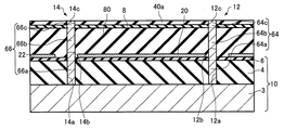
まず、本実施形態に係るテラヘルツ波検出装置について、図面を参照しながら説明する。図1は、本実施形態に係るテラヘルツ波検出装置100の単位セル102を模式的に示す断面図である。図2は、本実施形態に係るテラヘルツ波検出装置100の単位セル102を模式的に示す平面図である。図3は、本実施形態に係るテラヘルツ波検出装置100を模式的に示す平面図である。なお、図1は、図2のI−I線断面図である。また、図1〜図3では、互いに直交する3つの軸として、X軸、Y軸、およびZ軸を図示している。
1. First, a terahertz wave detection device according to this embodiment will be described with reference to the drawings. FIG. 1 is a cross-sectional view schematically showing a
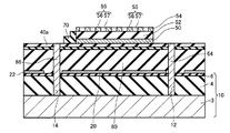
テラヘルツ波検出装置100は、図1〜図3に示すように、基板10と、反射層20と、支持部30,32と、支持基板(メンブレン)40と、第1金属層50と、焦電体層52と、第2金属層54と、配線層60,62と、コンタクト部64,66と、絶縁層70,72と、を含む。支持部30,32、支持基板40、金属層50,54、焦電体層52、配線層60,62、コンタクト部64,66、および絶縁層70,72は、単位セル102を構成している。なお、便宜上、図2では、絶縁層70,72を省略して図示している。また、便宜上、図3では、単位セル102を簡略化して図示している。
As shown in FIGS. 1 to 3, the terahertz
基板10の形状は、例えば、平板状である。基板10は、支持基板3と、層間絶縁層4と、第1保護層6と、を有している。支持基板3の厚さは、例えば、10μm以上500μm以下である。支持基板3の材質は、例えば、シリコンである。層間絶縁層4は、支持基板3上に設けられている。層間絶縁層4の厚さは、例えば、10nm以上10μm以下である。層間絶縁層4の材質は、例えば、酸化シリコンである。第1保護層6は、層間絶縁層4上に設けられている。第1保護層6の厚さは、例えば、10nm以上10μm以下である。第1保護層6の材質は、例えば、酸化アルミニウム(アルミナ)である。第1保護層6は、後述する犠牲層80をエッチングする際に、層間絶縁層4を保護することができる。
The shape of the
反射層20は、第1金属層50の下方に設けられている。図示の例では、反射層20は
、基板10上に設けられている。反射層20の厚さ(Z軸方向の大きさ)は、例えば、10nm以上1μm以下である。反射層20の材質は、例えば、金、銀、プラチナ、銅、アルミニウム、チタンである。反射層20は、焦電体層52において吸収されずに基板10に向かうテラヘルツ波を、焦電体層52に向けて反射させることができる。
The
なお、反射層20は、第1金属層50の下方に設けられていれば、支持基板3と層間絶縁層4との間に設けられていてもよいし、層間絶縁層4と第1保護層6との間に設けられていてもよい。
As long as the
また、図示の例では、基板10の、平面視において(Z軸方向からみて)単位セル102と重ならない領域には、層22が設けられている。層22は、反射層20と同じ材質である。反射層20と層22との間の距離D1(図1参照)は、例えば、1μm以上50μm以下である。
In the illustrated example, a
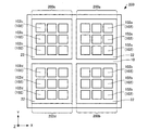
単位セル102は、基板10上に設けられている。単位セル102は、複数設けられている。図3に示す例では、9つの単位セル102が設けられているが、その数は特に限定されない。単位セル102は、例えば、マトリックス状に配列されている。隣り合う単位セル102の間の距離は、例えば、1μm以上50μm以下である。複数の単位セル102において、検出するテラヘルツ波の波長は、例えば、互いに同じである。
The
支持部30,32は、基板10上に設けられている。支持部30,32は、互いに離間している。支持部30,32の材質は、例えば、酸化シリコンである。支持部30,32は、支持基板40を基板10と離間して支持している。
The
支持基板40は、支持部30,32によって、基板10と離間して基板10の上方に支持されている。図示の例では、支持基板40は、反射層20と離間して設けられている。支持基板40と反射層20との間の距離は、例えば、100nm以上10μm以下である。
The
支持基板40は、例えば、二酸化シリコン層、窒化シリコン層、および二酸化シリコン層の3層構造を有している。図示の例では、支持基板40の下には、第2保護層8が設けられている。第2保護層8の厚さは、例えば、10nm以上10μm以下である。第2保護層8の材質は、例えば、酸化アルミニウムである。第2保護層8は、後述する犠牲層80をエッチングする際に、支持基板40を保護することができる。支持基板40は、基部42と、腕部44a,44bと、固定部46a,46bと、を有している。
The
基部42の形状は、例えば、平板状である。図2に示す例では、基部42の平面形状(Z軸方向からみた形状)は、正方形である。基部42のX軸方向の大きさは、例えば、5μm以上500μm以下である。基部42のY軸方向の大きさは、例えば、基部42のX軸方向の大きさと同じである。基部42の厚さは、例えば、10nm以上1μm以下である。基部42は、第1金属層50を支持している。
The shape of the
第1腕部44aは、基部42と第1固定部46aとを連結している。第2腕部44bは、基部42と第2固定部46bとを連結している。腕部44a,44bは、図2に示すように、基部42の互いに対向する面(側面)42a,42bから、互いに反対方向に延出し、直角に曲がって、固定部46a,46bに至っている。腕部44a,44bの幅W1(図2参照)は、例えば、500nm以上10μm以下である。第1腕部44aと基部42との間の距離D2(図2参照)は、例えば、500nm以上10μm以下である。第2腕部44bと基部42との間の距離は、例えば、D2と同じである。
The
固定部46a,46bは、支持部30,32上に設けられている。具体的には、第1固定部46aは、第1支持部30上に固定され、第2固定部46bは、第2支持部32上に固定されている。図2に示す例では、固定部46a,46bの平面形状は、正方形である。第1腕部44aのY軸方向の大きさと第1固定部46aのY軸方向の大きさとの和W3(図2参照)は、例えば、5μm以上500μm以下である。第2腕部44bのY軸方向の大きさと第2固定部46bのY軸方向の大きさとの和は、例えば、W3と同じである。
The fixing
第1金属層50は、基板10上方に設けられている。図示の例では、第1金属層50は、支持基板40の基部42上に設けられている。第1金属層50の厚さは、例えば、1nm以上500nm以下である。第1金属層50は、例えば、基部42側から順番に、イリジウム層、イリジウム酸化物層、および白金層を積層した3層構造を有している。第1金属層50は、焦電体層52に電気的に接続されている。第1金属層50は、焦電体層52の焦電流を検出するための一方の電極である。
The
焦電体層52は、第1金属層50上に設けられている。焦電体層52の厚さは、例えば、300nm以上700nm以下である。焦電体層52の材質は、焦電効果を発揮することができる誘電体である。具体的には、焦電体層52の材質は、チタン酸ジルコン酸鉛(PZT)である。焦電体層52は、焦電体層52に入射するテラヘルツ波を吸収して熱に変換し、かつ、変換された熱を電気信号に変換することができる。
The
第2金属層54は、焦電体層52上に設けられている。第2金属層54の平面形状は、例えば、正方形である。第2金属層54のX軸方向の大きさは、例えば、5μm以上500μm以下である。第2金属層54のY軸方向の大きさは、例えば、第2金属層54のX軸方向の大きさと同じである。第2金属層54のX軸方向の大きさおよびY軸方向の大きさが、10nmより小さいと、焦電体層52におけるテラヘルツ波の吸収効率が低下する場合がある。第2金属層54のX軸方向の大きさおよびY軸方向の大きさが、200μmより大きいと、支持部30,32によって、支持基板40を基板10と離間して支持できない場合がある。第2金属層54の厚さは、例えば、1nm以上500nm以下である。
The
第2金属層54は、例えば、焦電体層52側から順番に、白金層、イリジウム酸化物層、およびイリジウム層を積層した3層構造を有している。第2金属層54は、焦電体層52に電気的に接続されている。第2金属層54は、焦電体層52の焦電流を検出するための他方の電極である。金属層50,54のテラヘルツ波に対する反射率は、例えば、90%以上である。
For example, the
なお、金属層50,54の材質は、上記の例に限定されず、例えば、金、銅、鉄、アルミニウム、亜鉛、クロム、鉛、チタンなどの金属や、ニクロムなどの合金であってもよい。 In addition, the material of the metal layers 50 and 54 is not limited to said example, For example, metals, such as gold | metal | money, copper, iron, aluminum, zinc, chromium, lead, titanium, and alloys, such as nichrome, may be sufficient. .
第2金属層54は、単位構造55が所定の周期で設けられた周期構造を有している。単位構造55は、メタマテリアルの一部である。ここで、メタマテリアルとは、電磁波(テラヘルツ波)の波長に比べて十分に小さい単位構造が周期的に配列されていて、電磁波に対して均質な媒質として振舞うように構成された人工物質のことである。メタマテリアルは、単位構造の構造・配置によって、自由にその物性値(誘電率・透磁率)を調整することができる。
The
単位構造55は、焦電体層52上に第2金属層54が設けられている第1領域56と、焦電体層52上に第2金属層54が設けられていない第2領域57と、を有している。図示の例では、第1領域56の平面形状、および第2領域57の平面形状は、正方形である。第2領域57は、第2金属層54に開口部(第2金属層54を貫通する開口部)が設け
られることによって、形成される領域である。
The
単位構造55は、例えば、X軸方向に周期Tの長さで周期的に設けられている。言い換えると、X軸方向において、大きさ(幅)Lの第1領域56、大きさ(幅)Dの第2領域57が交互に配列され、LとDとの和はT(L+D=T)である。単位構造55は、例えば、Y軸方向に周期Tの長さで周期的に設けられている。言い換えると、Y軸方向において、幅Lの第1領域56、幅Dの第2領域57が交互に配列され、LとDとの和はT(L+D=T)である。
The
単位構造55の周期Tは、焦電体層52にて吸収されるテラヘルツ波の真空中における波長よりも短い。すなわち、単位構造55の第1領域56の幅Lおよび第2領域57の幅Dは、焦電体層52にて吸収されるテラヘルツ波の真空中における波長よりも短い。第1領域56の幅Lは、例えば、0.1μm以上3μm以下である。幅Lの値によって、焦電体層52において吸収されるテラヘルツ波の波長(周波数)が決定される。第2領域57の幅Dは、例えば、0.1μm以上3μm以下である。幅Dによって、焦電体層52において吸収されるテラヘルツ波の吸収率が決定される。
The period T of the
第1配線層60は、第1腕部44a上に設けられている。第1配線層60は、第1金属層50および第1コンタクト部64に接続されている。第2配線層62は、第2腕部44b上に設けられている。第2配線層62は、第2金属層54および第2コンタクト部66に接続されている。配線層60,62の幅W2(図2参照)は、例えば、500nm以上10μm以下である。配線層60,62の厚さは、例えば、10nm以上100nm以下である。配線層60,62の材質は、導電性であれば、特に限定されない。配線層60,62は、ワイヤーボンディングであってもよい。
The
第1コンタクト部64は、第1固定部46a、第2保護層8、第1支持部30、第1保護層6、および層間絶縁層4に形成された第1コンタクトホール12に設けられている。第2コンタクト部66は、第2固定部46b、第2保護層8、第2支持部32、第1保護層6、および層間絶縁層4に形成された第2コンタクトホール14に設けられている。コンタクト部64,66の厚さは、例えば、100nm以上10μm以下である。コンタクト部64,66の材質は、導電性であれば、特に限定されない。
The
コンタクト部64,66は、例えば支持基板3上に設けられた図示せぬ回路部と電気的に接続されている。コンタクト部64,66によって、金属層50,54と回路部とを電気的に接続させることができる。
The
絶縁層70,72は、焦電体層52を覆って設けられている。図示の例では、第1絶縁層70は、焦電体層52の側方および第1金属層50の側方に設けられている。第2絶縁層72は、焦電体層52の側方および第2金属層54の側方、並びに焦電体層52上および第2金属層54上に設けられている。第2絶縁層72の厚さ(第2金属層54上における第2絶縁層72の厚さ)は、例えば、1nm以上100nm以下である。絶縁層70,72の材質は、例えば、酸化アルミニウム、酸化シリコンである。絶縁層70,72は、焦電体層52および金属層50,54に異物が付着することを抑制することができる。さらに、絶縁層70,72は、焦電体層52および金属層50,54が酸化することを抑制することができる。
The insulating layers 70 and 72 are provided so as to cover the
次に、テラヘルツ波検出装置100の動作について説明する。
Next, the operation of the terahertz
テラヘルツ波検出装置100の単位セル102にテラヘルツ波が照射されると、第2金属層54の単位構造55の周期Tは、テラヘルツ波の波長よりも短いため、テラヘルツ波
は、焦電体層52に進入し、単位構造55と第1金属層50との間で多重反射する。具体的には、単位構造55の焦電体層52との接触面と、第1金属層50の焦電体層52との接触面と、の間で多重反射して共振現象が起こり、定在波が生じる。共振するテラヘルツ波の周波数(共振周波数)は、単位構造55の形状や大きさによって適宜変更することができる。このように、テラヘルツ波検出装置100では、焦電体層52内にテラヘルツ波を閉じ込めることができる。
When the
焦電体層52内に閉じ込められたテラヘルツ波が、焦電体層52を挟む単位構造55と第1金属層50との間を多重反射することにより、焦電体層52に誘電損失が生じ、これにより熱が発生する。このように、焦電体層52は、テラヘルツ波を吸収して熱に変換することができる。また、単位構造55の焦電体層52との接触面を構成する原子および電子、および第1金属層50の焦電体層52との接触面を構成する原子および電子が振動し、これにより熱が発生する。
The terahertz wave confined in the
焦電体層52では、発生した熱によって温度変化が生じる。そして、焦電体層52の温度変化に応じて、焦電体層52の電気分極量の変化分が、焦電流として金属層50,54に流れる。このように、焦電体層52は、温度変化を(熱を)電気信号に変換することができる。
In the
焦電体層52の焦電効果に応じて金属層50,54に流れる電流(電気信号)は、支持基板3に設けられた回路部(図示せず)に至る。回路部では、該電気信号からテラヘルツ波を検出する。以上により、テラヘルツ波検出装置100は、テラヘルツ波を検出することができる。
A current (electric signal) flowing in the metal layers 50 and 54 in accordance with the pyroelectric effect of the
なお、テラヘルツ波検出装置100では、隣り合う単位構造55において、一方の単位構造55と第1金属層50との間に生じた定在波と、他方の単位構造55と第1金属層50との間に生じた定在波と、の間で電気的カップリングが生じる。これにより、焦電体層52におけるテラヘルツ波の吸収率を向上させることができる。
In the terahertz
また、テラヘルツ波検出装置100では、単位構造55と第1金属層50との間だけでなく、例えば、隣り合う単位構造55間においてもテラヘルツ波が多重反射し、共振現象が生じる。
Further, in the terahertz
テラヘルツ波検出装置100は、例えば、以下の特徴を有する。
The terahertz
テラヘルツ波検出装置100では、第2金属層54は、単位構造55が所定の周期Tで設けられた周期構造を有し、焦電体層52は、焦電体層52に入射するテラヘルツ波を吸収して熱に変換し、かつ、変換された熱を電気信号に変換する。そのため、テラヘルツ波検出装置100では、テラヘルツ波を吸収して熱に変換する部分と、変換された熱を電気信号に変換する部分と、を別々に設けている場合に比べて、熱容量を小さくして、テラヘルツ波検出装置100の反応速度(応答速度)を速くすることができる。
In the terahertz
例えば、テラヘルツ波を吸収して熱に変換する第1部分と、変換された熱を電気信号に変換する第2部分と、を別々に設けている場合では、第1部分の熱を第2部分に伝える必要があり、その分タイムロスとなって、テラヘルツ波検出装置の反応速度が遅くなる場合がある。 For example, in the case where a first part that absorbs terahertz waves and converts it into heat and a second part that converts the converted heat into an electrical signal are provided separately, the heat of the first part is converted into the second part. Therefore, there is a case where a time loss is caused and the reaction speed of the terahertz wave detection device is slowed down.
さらに、テラヘルツ波検出装置100では、外部から電流や電圧を印加することなく、テラヘルツ波に起因する電気信号を検出することができるので、電流や電圧を印加することによるノイズが発生しない。したがって、テラヘルツ波検出装置100は、電気的なノ
イズによる検出感度の低下を抑制することができる。
Furthermore, since the terahertz
テラヘルツ波検出装置100では、単位構造55の所定の周期Tは、焦電体層52にて吸収されるテラヘルツ波の真空中における波長よりも短い。そのため、テラヘルツ波検出装置100の単位セル102に照射されたテラヘルツ波は、焦電体層52に進入し、単位構造55と第1金属層50との間で多重反射することができる。
In the terahertz
テラヘルツ波検出装置100では、第1金属層50および第2金属層54は、焦電体層52に電気的に接続されている。そのため、テラヘルツ波検出装置100では、焦電体層52の温度変化に応じて、焦電体層52の電気分極量の変化分は、焦電流として金属層50,54に流れることができる。
In the terahertz
テラヘルツ波検出装置100では、第1金属層50を支持する支持基板40と、支持基板40を基板10と離間して支持する支持部30,32と、を含む。そのため、テラヘルツ波検出装置100では、焦電体層52を基板10から熱的に分離することができる。したがって、テラヘルツ波検出装置100では、複数の単位セル102間において、熱が伝達することを抑制することができる。さらに、テラヘルツ波検出装置100では、テラヘルツ波の照射による焦電体層の温度変化を精度よく検出することができる 。
The terahertz
テラヘルツ波検出装置100では、焦電体層52の厚さは、例えば、300nm以上700nm以下である。そのため、テラヘルツ波検出装置100では、焦電体層52において、より確実に、テラヘルツ波を吸収し、テラヘルツ波検出装置100の反応速度を速くすることができる。焦電体層の厚さが300nmより小さい場合は、焦電体層において十分にテラヘルツ波を吸収できない場合がある。焦電体層の厚さが700nmより大きい場合は、焦電体層において完全に分極するまでに時間がかかり、テラヘルツ波検出装置の反応速度が遅くなる場合がある。さらに、焦電体層の厚さが700nmより大きい場合は、焦電体層にクラックが発生する場合がある。
In the terahertz
テラヘルツ波検出装置100では、第1金属層50、焦電体層52、および第2金属層54は、単位セル102を構成し、単位セル102は、複数設けられている。そのため、テラヘルツ波検出装置100では、例えば隣り合う単位セル102の間の距離を小さくすることにより、単位セルが1つしか設けられていない場合に比べて、テラヘルツ波検出装置100全体としてのテラヘルツ波の吸収効率を高くすることができる。これにより、テラヘルツ波検出装置100の高感度化を図ることができる。
In the terahertz
テラヘルツ波検出装置100では、第1金属層50の下方にテラヘルツ波を反射する反射層20を含む。そのため、テラヘルツ波検出装置100では、反射層20よって、焦電体層52において吸収されずに基板10に向かうテラヘルツ波を、焦電体層52に向けて反射させることができる。これにより、焦電体層52におけるテラヘルツ波の吸収効率を高くすることができ、テラヘルツ波検出装置100の高感度化を図ることができる。
The terahertz
2. テラヘルツ波検出装置の製造方法
次に、本実施形態に係るテラヘルツ波検出装置の製造方法について、図面を参照しながら説明する。図4〜図9は、本実施形態に係るテラヘルツ波検出装置100の製造工程を模式的に示す断面図であって、図1に対応している。
2. Method for Manufacturing Terahertz Wave Detection Device Next, a method for manufacturing the terahertz wave detection device according to the present embodiment will be described with reference to the drawings. 4 to 9 are cross-sectional views schematically showing the manufacturing process of the terahertz
図4に示すように、支持基板3上に、層間絶縁層4を形成する。層間絶縁層4は、例えば、CVD(Chemical Vapor Deposition)法により形成される。 As shown in FIG. 4, an interlayer insulating layer 4 is formed on the support substrate 3. The interlayer insulating layer 4 is formed by, for example, a CVD (Chemical Vapor Deposition) method.
次に、層間絶縁層4をパターニング(フォトリソグラフィーおよびエッチングによるパターニング)して、コンタクトホール12a,14aを形成する。次に、コンタクトホール12a,14aに、それぞれコンタクト部64a,66aを形成する。コンタクト部64a,66aは、例えば、めっき法、スパッタ法により形成される。
Next, the interlayer insulating layer 4 is patterned (patterning by photolithography and etching) to form
図5に示すように、層間絶縁層4上に、第1保護層6を形成する。第1保護層6は、例えば、CVD法、スパッタ法により形成される。これにより、支持基板3、層間絶縁層4、および第1保護層6を有する基板10を形成することができる。
As shown in FIG. 5, the first protective layer 6 is formed on the interlayer insulating layer 4. The first protective layer 6 is formed by, for example, a CVD method or a sputtering method. Thereby, the board |
次に、第1保護層6上に、反射層20および層22を形成する。反射層20および層22は、例えば、導電層(図示せず)をスパッタ法や真空蒸着法などにより成膜した後、該導電層をパターニングすることにより形成される。
Next, the
次に、第1保護層6上、反射層20上、および層22上に、犠牲層80を形成する。犠牲層80は、例えば、CVD法により形成される。犠牲層80材質は、例えば、酸化シリコンである。
Next, a
次に、犠牲層80および第1保護層6をパターニングして、コンタクトホール12b,14bを形成する。コンタクトホール12b,14bは、それぞれコンタクト部64a,66aが露出するように形成される。次に、コンタクトホール12b,14bに、それぞれコンタクト部64b,66bを形成する。コンタクト部64b,66bは、それぞれコンタクト部64a,66aに接続されるように形成される。コンタクト部64b,66bは、例えば、めっき法、スパッタ法により形成される。
Next, the
図6に示すように、犠牲層80上に第2保護層8を形成する。第2保護層8は、例えば、CVD法、スパッタ法により形成される。次に、第2保護層8上に、支持基板40となる層40aを形成する。層40aは、例えば、CVD法、スパッタ法により形成される。
As shown in FIG. 6, the second
次に、第2保護層8および層40aをパターニングして、コンタクトホール12c,14cを形成する。コンタクトホール12c,14cは、それぞれコンタクト部64b,66bが露出するように形成される。次に、コンタクトホール12c,14cに、それぞれコンタクト部64c,66cを形成する。コンタクト部64c,66cは、それぞれコンタクト部64b,66bに接続されるように形成される。コンタクト部64c,66cは、例えば、めっき法、スパッタ法により形成される。
Next, the second
以上の工程により、コンタクトホール12a,12b,12cからなる第1コンタクトホール12、およびコンタクトホール14a,14b,14cからなる第2コンタクトホール14を形成することができる。また、コンタクト部64a,64b,64cからなる第1コンタクト部64、およびコンタクト部66a,66b,66cからなる第2コンタクト部66を形成することができる。
Through the steps described above, the
図7に示すように、層40a上に、第1金属層50、焦電体層52、および第2金属層54を、この順で形成する。金属層50,54は、例えば、スパッタ法による成膜、およびパターニングによって形成される。第2金属層54は、第1領域56および第2領域57を有する単位構造55が複数設けられるように形成される。焦電体層52は、例えば、スパッタ法やゾルゲル法による成膜、およびパターニングによって形成される。
As shown in FIG. 7, the
次に、層40a上であって、第1金属層50の側方および焦電体層52の側方に、第1絶縁層70を形成する。第1絶縁層70は、例えば、スパッタ法やCVD法による成膜、およびパターニングによって形成される。
Next, the first insulating
図8に示すように、層40a上に第1配線層60を形成して、第1金属層50と第1コンタクト部64とを電気的に接続する。さらに、層40a上および第1絶縁層70上に第2配線層62を形成して、第2金属層54と第2コンタクト部66とを電気的に接続する。配線層60,62は、例えば、めっき法、スパッタ法により形成される。
As shown in FIG. 8, a
次に、第2金属層54上および焦電体層52上に第2絶縁層72を形成する。第2絶縁層72は、例えば、スパッタ法やCVD法による成膜、およびパターニングによって形成される。
Next, the second insulating
図9に示すように、層40aおよび第2保護層8をパターニングする。これにより、基部42、腕部44a,44b、および固定部46a,46bを有する支持基板40を形成することができる。
As shown in FIG. 9, the
図1に示すように、犠牲層80を除去する。犠牲層80の除去は、例えば、支持基板40をマスクとしたエッチングによって行う。これにより、支持部30,32を形成することができる。
As shown in FIG. 1, the
以上の工程により、テラヘルツ波検出装置100を製造することができる。
Through the above steps, the terahertz
3. テラヘルツ波検出装置の変形例
次に、本実施形態の変形例に係るテラヘルツ波検出装置について、図面を参照しながら説明する。図10は、本実施形態の変形例に係るテラヘルツ波検出装置200を模式的に示す平面図である。なお、便宜上、図10では、単位セル102を簡略化して図示している。また、図10では、互いに直交する3つの軸として、X軸、Y軸、およびZ軸を図示している。
3. Modification of Terahertz Wave Detection Device Next, a terahertz wave detection device according to a modification of the present embodiment will be described with reference to the drawings. FIG. 10 is a plan view schematically showing a terahertz
以下、本実施形態の変形例に係るテラヘルツ波検出装置200において、本実施形態に係るテラヘルツ波検出装置100の構成部材と同様の機能を有する部材については同一の符号を付し、その詳細な説明を省略する。
Hereinafter, in the terahertz
テラヘルツ波検出装置200では、単位構造55の第2領域57の幅Dが異なる複数の単位セル102が複数設けられている点において、上述したテラヘルツ波検出装置100と異なる。
The terahertz
テラヘルツ波検出装置200では、図10に示すように、4つの領域200a,200b,200c,200dを有し、領域200a,200b,200c,200dに、それぞれ単位セル102a,102b,102c,102dが設けられている。図示の例では、領域200a,200b,200c,200dの平面形状は、正方形である。領域200a,200b,200c,200dは、図10に示すように、基板10上に設けられた層22によって、区画された領域であってもよい。単位セル102a,102b,102c,102dは、それぞれ領域200a,200b,200c,200dにおいて複数設けられている。
As shown in FIG. 10, the terahertz
単位セル102a,102b,102c,102dでは、互いに、単位構造55の第2領域57の幅Dが異なっている。すなわち、テラヘルツ波検出装置200では、第2領域57の幅Dが異なる4種類の単位セル102が設けられている。なお、単位セル102の種類は、4種類に限定されない。
In the
テラヘルツ波検出装置200では、単位構造55の第2領域57の幅Dが異なる複数の
単位セル102が複数設けられている。そのため、テラヘルツ波検出装置200は、異なる周波数(異なる波長)のテラヘルツ波を検出することができる。
In the terahertz
テラヘルツ波検出装置200では、テラヘルツ波検出装置100と同様に、熱容量を小さくして、反応速度を速くすることができる。
In the terahertz
4. イメージング装置
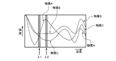
次に、本実施形態に係るイメージング装置300について、図面を参照しながら説明する。図11は、本実施形態に係るイメージング装置300を示すブロック図である。図12は、本実施形態に係るイメージング装置300のテラヘルツ波検出部320を模式的に示す平面図である。図13は、対象物のテラヘルツ帯でのスペクトルを示すグラフである。図14は、対象物の物質A、B、およびCの分布を示す画像の図である。
4). Imaging Device Next, an
イメージング装置300は、図11に示すように、テラヘルツ波を発生するテラヘルツ波発生部310と、テラヘルツ波発生部310から射出され、対象物Oを透過したテラヘルツ波または対象物Oで反射されたテラヘルツ波を検出するテラヘルツ波検出部320と、テラヘルツ波検出部320の検出結果に基づいて、対象物Oの画像、すなわち、画像データを生成する画像形成部330と、を含む。
As shown in FIG. 11, the
テラヘルツ波発生部310としては、例えば、量子カスケードレーザー、光伝導アンテナと短パルスレーザーとを用いた方式、非線形光学結晶を用いた差周波数発生方式を用いる。
As the terahertz
テラヘルツ波検出部320は、本発明に係るテラヘルツ波検出装置を有する。以下では、本発明に係るテラヘルツ波検出装置として、テラヘルツ波検出装置200を有する例について説明する。なお、便宜上、図12では、テラヘルツ波検出装置200を簡略化して図示している。
The terahertz
テラヘルツ波検出部320は、図12に示すように、複数の画素322を含む。図示の例では、画素322の形状は、正方形である。画素322は、マトリックス状に配置されている。画素322の数は、特に限定されない。画素322は、テラヘルツ波検出装置200により構成されている。
The terahertz
テラヘルツ波検出装置200では、上述のように、領域200a,200b,200c,200dに、それぞれ設けられた単位セル102a,102b,102c,102dによって、互いに異なる波長のテラヘルツ波を選択的に検出することができる。すなわち、各画素322において、4つの波長のテラヘルツ波を検出することができる。
In the terahertz
次に、イメージング装置300の使用例について説明する。
Next, a usage example of the
まず、分光イメージングの対象となる対象物Oが、3つの物質A、B、およびCで構成されているとする。イメージング装置300は、この対象物Oの分光イメージングを行う。また、ここでは、一例として、テラヘルツ波検出部320は、対象物Oで反射されたテラヘルツ波を検出することとする。
First, it is assumed that an object O to be subjected to spectral imaging is composed of three substances A, B, and C. The
また、テラヘルツ波検出部320の各画素322においては、テラヘルツ波検出装置200の領域200aに設けられた単位セル102aおよび領域200bに設けられた単位セル102bを使用する。単位セル102aにおいて検出される波長(吸収される波長)をλ1、単位セル102bにおいて検出される波長(吸収される波長)をλ2とし、対象物Oで反射されたテラヘルツ波の波長λ1の成分の強度をα1、波長λ2の成分の強度を
α2としたとき、その強度α2と強度α1の差分(α2−α1)が、物質Aと物質Bと物質Cとで、互いに顕著に区別できるように、単位セル102aにおいて検出される波長λ1、および単位セル102bで検出される波長λ2が設定されている。
In each
図13に示すように、物質Aにおいては、対象物Oで反射したテラヘルツ波の波長λ2の成分の強度α2と波長λ1の成分の強度α1との差分(α2−α1)は、正値となる。また、物質Bにおいては、強度α2と強度α1との差分(α2−α1)は、零となる。また、物質Cにおいては、強度α2と強度α1との差分(α2−α1)は、負値となる。 As shown in FIG. 13, in the substance A, the difference (α2−α1) between the intensity α2 of the component of the wavelength λ2 of the terahertz wave reflected by the object O and the intensity α1 of the component of the wavelength λ1 is a positive value. . In the substance B, the difference (α2−α1) between the strength α2 and the strength α1 is zero. In the substance C, the difference (α2−α1) between the strength α2 and the strength α1 is a negative value.
イメージング装置300により、対象物Oの分光イメージングを行う際は、まず、テラヘルツ波発生部310により、テラヘルツ波を発生し、そのテラヘルツ波を対象物Oに照射する。そして、対象物Oで反射されたテラヘルツ波をテラヘルツ波検出部320で、α1およびα2として検出する。この検出結果は、画像形成部330に送出される。なお、この対象物Oへのテラヘルツ波の照射および対象物Oで反射したテラヘルツ波の検出は、対象物Oの全体に対して行う。
When spectral imaging of the object O is performed by the
画像形成部330においては、前記検出結果に基づいて、単位セル102bにおいて検出されたテラヘルツ波の波長λ2の成分の強度α2と、単位セル102aにおいて検出されたテラヘルツ波の波長λ1の成分の強度α1と、の差分(α2−α1)を求める。そして、対象物Oのうち、前記差分が正値となる部位を物質A、前記差分が零となる部位を物質B、前記差分が負値となる部位を物質Cと判断し、特定する。
In the
また、画像形成部330では、図14に示すように、対象物Oの物質A、B、およびCの分布を示す画像の画像データを作成する。この画像データは、画像形成部330から図示しないモニターに送出され、そのモニターにおいて、対象物Oの物質A、B、およびCの分布を示す画像が表示される。この場合、例えば、対象物Oの物質Aの分布する領域は黒色、物質Bの分布する領域は灰色、物質Cの分布する領域は白色に色分けして表示される。このイメージング装置300では、以上のように、対象物Oを構成する各物質の同定と、その各部質の分布測定とを同時に行うことができる。イメージング装置300は、例えば、薬剤検査に用いられる。
In addition, the
なお、イメージング装置300の用途は、上記のものに限らず、例えば、人物に対してテラヘルツ波を照射し、その人物を透過または反射したテラヘルツ波を検出し、画像形成部330において処理を行うことにより、その人物が、拳銃、ナイフ、違法な薬物等を所持しているか否かを判別することもできる。
The application of the
イメージング装置300では、熱容量を小さくして、反応速度を速くすることができるテラヘルツ波検出装置200を含む。そのため、イメージング装置300は、反応速度を速くすることができる。
The
5. 計測装置
次に、本実施形態に係る計測装置400について、図面を参照しながら説明する。図15は、本実施形態に係る計測装置400を示すブロック図である。
5. Measuring Device Next, a measuring
以下、本実施形態に係る計測装置400において、本実施形態に係るイメージング装置300の構成部材と同様の機能を有する部材については同一の符号を付し、その詳細な説明を省略する。このことは、以下に示す本実施形態に係るカメラ500においても同様である。
Hereinafter, in the
計測装置400は、図15に示すように、テラヘルツ波を発生するテラヘルツ波発生部
310と、テラヘルツ波発生部310から射出され、対象物Oを透過するテラヘルツ波または対象物Oで反射されたテラヘルツ波を検出するテラヘルツ波検出部320と、テラヘルツ波検出部320の検出結果に基づいて、対象物Oを計測する計測部410と、を含む。
As shown in FIG. 15, the measuring
次に、計測装置400の使用例について説明する。計測装置400により、対象物Oの分光計測を行う際は、まず、テラヘルツ波発生部310により、テラヘルツ波を発生させ、そのテラヘルツ波を対象物Oに照射する。そして、対象物Oを透過したテラヘルツ波または対象物Oで反射されたテラヘルツ波をテラヘルツ波検出部320で検出する。この検出結果は、計測部410に送出される。なお、この対象物Oへのテラヘルツ波の照射および対象物Oを透過したテラヘルツ波または対象物Oで反射されたテラヘルツ波の検出は、対象物Oの全体に対して行う。
Next, a usage example of the measuring
計測部410においては、前記検出結果から、各画素322を構成するテラヘルツ波検出装置200の単位セル102a,102b,102c,102dにおいて検出されたテラヘルツ波のそれぞれの強度を把握し、対象物Oの成分およびその分布の分析等を行う。
In the
計測装置400では、熱容量を小さくして、反応速度を速くすることができるテラヘルツ波検出装置200を含む。そのため、計測装置400は、反応速度を速くすることができる。
The
6. カメラ
次に、本実施形態に係るカメラ500について、図面を参照しながら説明する。図16は、本実施形態に係るカメラ500を示すブロック図である。図17は、本実施形態に係るカメラ500を模式的に示す斜視図である。
6). Camera Next, the
カメラ500は、図16および図17に示すように、テラヘルツ波を発生するテラヘルツ波発生部310と、テラヘルツ波発生部310から射出され、対象物Oで反射されたテラヘルツ波または対象物Oを透過したテラヘルツ波を検出するテラヘルツ波検出部320と、テラヘルツ波検出部320の検出結果を記憶する記憶部510と、を含む。そして、これらの各部310,320,510は、カメラ500の筐体520に収められている。また、カメラ500は、対象物Oで反射したテラヘルツ波をテラヘルツ波検出部320に収束(結像)させるレンズ(光学系)530と、テラヘルツ波発生部310で発生したテラヘルツ波を筐体520の外部へ出射させるための窓部540と、を備える。レンズ530や窓部540は、テラヘルツ波を透過・屈折させるシリコン、石英、ポリエチレンなどの部材によって構成されている。なお、窓部540は、スリットのように単に開口が設けられている構成としてもよい。
As shown in FIGS. 16 and 17, the
次に、カメラ500の使用例について説明する。カメラ500により、対象物Oを撮像する際は、まず、テラヘルツ波発生部310により、テラヘルツ波を発生させ、そのテラヘルツ波を対象物Oに照射する。そして、対象物Oで反射されたテラヘルツ波をレンズ530によってテラヘルツ波検出部320に収束(結像させて)検出する。この検出結果は、記憶部510に送出され、記憶される。なお、この対象物Oへのテラヘルツ波の照射および対象物Oで反射されたテラヘルツ波の検出は、対象物Oの全体に対して行う。また、前記検出結果は、例えば、パーソナルコンピューター等の外部装置に送信することもできる。パーソナルコンピューターでは、前記検出結果に基づいて、各処理を行うことができる。
Next, a usage example of the
カメラ500では、熱容量を小さくして、反応速度を速くすることができるテラヘルツ波検出装置200を含む。そのため、カメラ500は、反応速度を速くすることができる
。
The
上述した実施形態および変形例は一例であって、これらに限定されるわけではない。例えば、各実施形態および各変形例を適宜組み合わせることも可能である。 The above-described embodiments and modifications are merely examples, and the present invention is not limited to these. For example, it is possible to appropriately combine each embodiment and each modification.
本発明は、実施の形態で説明した構成と実質的に同一の構成(例えば、機能、方法及び結果が同一の構成、あるいは目的及び効果が同一の構成)を含む。また、本発明は、実施の形態で説明した構成の本質的でない部分を置き換えた構成を含む。また、本発明は、実施の形態で説明した構成と同一の作用効果を奏する構成又は同一の目的を達成することができる構成を含む。また、本発明は、実施の形態で説明した構成に公知技術を付加した構成を含む。 The present invention includes configurations that are substantially the same as the configurations described in the embodiments (for example, configurations that have the same functions, methods, and results, or configurations that have the same objects and effects). In addition, the invention includes a configuration in which a non-essential part of the configuration described in the embodiment is replaced. In addition, the present invention includes a configuration that exhibits the same operational effects as the configuration described in the embodiment or a configuration that can achieve the same object. Further, the invention includes a configuration in which a known technique is added to the configuration described in the embodiment.
3…支持基板、4…層間絶縁層、6…第1保護層、8…第2保護層、10…基板、12…第1コンタクトホール、12a,12b,12c…コンタクトホール、14…第2コンタクトホール、14a,14b,14c…コンタクトホール、20…反射層、22…層、30…第1支持部、32…第2支持部、40…支持基板、42…基部、42a,42b…面、44a…第1腕部、44b…第2腕部、46a…第1固定部、46b…第2固定部、50…第1金属層、52…焦電体層、54…第2金属層、55…単位構想、56…第1領域、57…第2領域、60…第1配線、62…第2配線、64…第1コンタクト部、64a,64b,64c…コンタクト部、66…第2コンタクト部、66a,66b,66c…コンタクト部、70…第1絶縁層、72…第2絶縁層、80…犠牲層、100…テラヘルツ波検出装置、102,102a,102b,102c,102d…単位セル、200…テラヘルツ波検出装置、200a,200b,200c,200d…領域、300…イメージング装置、310…テラヘルツ波発生部、320…テラヘルツ波検出部、322…画素、330…画像形成部、400…計測装置、410…計測部、500…カメラ、510…記憶部、520…筐体、530…レンズ、540…窓部
DESCRIPTION OF SYMBOLS 3 ... Support substrate, 4 ... Interlayer insulation layer, 6 ... 1st protective layer, 8 ... 2nd protective layer, 10 ... Board | substrate, 12 ... 1st contact hole, 12a, 12b, 12c ... Contact hole, 14 ...
Claims (11)
前記基板上方に設けられた第1金属層と、
前記第1金属層上に設けられた焦電体層と、
前記焦電体層上に設けられた第2金属層と、
を含み、
前記第2金属層は、単位構造が所定の周期で設けられた周期構造を有し、
前記焦電体層は、前記焦電体層に入射するテラヘルツ波を吸収して熱に変換し、かつ、変換された熱を電気信号に変換する、ことを特徴とするテラヘルツ波検出装置。 A substrate,
A first metal layer provided above the substrate;
A pyroelectric layer provided on the first metal layer;
A second metal layer provided on the pyroelectric layer;
Including
The second metal layer has a periodic structure in which unit structures are provided at a predetermined period,
The terahertz wave detecting device, wherein the pyroelectric layer absorbs a terahertz wave incident on the pyroelectric layer and converts it into heat, and converts the converted heat into an electric signal.
前記支持基板を前記基板と離間して支持する支持部と、
を含む、ことを特徴とする請求項1ないし3のいずれか1項に記載のテラヘルツ波検出装置。 A support substrate for supporting the first metal layer;
A support portion for supporting the support substrate apart from the substrate;
The terahertz wave detection device according to claim 1, wherein the terahertz wave detection device includes:
前記単位セルは、複数設けられている、ことを特徴とする請求項1ないし5のいずれか1項に記載のテラヘルツ波検出装置。 The first metal layer, the pyroelectric layer, and the second metal layer constitute a unit cell,
The terahertz wave detection device according to claim 1, wherein a plurality of the unit cells are provided.
前記焦電体層上に前記第2金属層が設けられている領域と、
前記焦電体層上に前記第2金属層が設けられていない領域と、
を有し、
前記第2金属層が設けられていない領域の幅が異なる複数の前記単位セルが設けられている、ことを特徴とする請求項6に記載のテラヘルツ波検出装置。 The unit structure is
A region where the second metal layer is provided on the pyroelectric layer;
A region where the second metal layer is not provided on the pyroelectric layer;
Have
The terahertz wave detection device according to claim 6, wherein a plurality of the unit cells having different widths in a region where the second metal layer is not provided are provided.
前記テラヘルツ波発生部から射出され、対象物を透過した前記テラヘルツ波または対象物で反射された前記テラヘルツ波を検出する請求項1ないし8のいずれか1項に記載のテラヘルツ波検出装置を有するテラヘルツ波検出部と、
前記テラヘルツ波検出部の検出結果を記憶する記憶部と、
を含む、ことを特徴とするカメラ。 A terahertz wave generator for generating the terahertz wave;
The terahertz wave having the terahertz wave detection device according to claim 1, wherein the terahertz wave emitted from the terahertz wave generation unit and transmitted through the object or the terahertz wave reflected by the object is detected. A wave detector;
A storage unit for storing a detection result of the terahertz wave detection unit;
Including a camera.
前記テラヘルツ波発生部から射出され、対象物を透過した前記テラヘルツ波または対象物で反射された前記テラヘルツ波を検出する請求項1ないし8のいずれか1項に記載のテラヘルツ波検出装置を有するテラヘルツ波検出部と、
前記テラヘルツ波検出部の検出結果に基づいて、前記対象物の画像を生成する画像形成部と、
を含む、ことを特徴とするイメージング装置。 A terahertz wave generator for generating the terahertz wave;
The terahertz wave having the terahertz wave detection device according to claim 1, wherein the terahertz wave emitted from the terahertz wave generation unit and transmitted through the object or the terahertz wave reflected by the object is detected. A wave detector;
An image forming unit that generates an image of the object based on a detection result of the terahertz wave detection unit;
An imaging apparatus comprising:
前記テラヘルツ波発生部から射出され、対象物を透過した前記テラヘルツ波または対象物で反射された前記テラヘルツ波を検出する請求項1ないし8のいずれか1項に記載のテラヘルツ波検出装置を有するテラヘルツ波検出部と、
前記テラヘルツ波検出部の検出結果に基づいて、前記対象物を計測する計測部と、
を含む、ことを特徴とする計測装置。 A terahertz wave generator for generating the terahertz wave;
The terahertz wave having the terahertz wave detection device according to claim 1, wherein the terahertz wave emitted from the terahertz wave generation unit and transmitted through the object or the terahertz wave reflected by the object is detected. A wave detector;
Based on the detection result of the terahertz wave detection unit, a measurement unit that measures the object,
A measuring device comprising:
Priority Applications (3)
| Application Number | Priority Date | Filing Date | Title |
|---|---|---|---|
| JP2014194032A JP2016065767A (en) | 2014-09-24 | 2014-09-24 | Terahertz wave detection device, camera, imaging device and measurement device |
| CN201510601469.5A CN105445186A (en) | 2014-09-24 | 2015-09-18 | Terahertz wave detecting device, camera, imaging apparatus, and measuring apparatus |
| US14/863,371 US9638578B2 (en) | 2014-09-24 | 2015-09-23 | Terahertz wave detecting device, camera, imaging apparatus, and measuring apparatus |
Applications Claiming Priority (1)
| Application Number | Priority Date | Filing Date | Title |
|---|---|---|---|
| JP2014194032A JP2016065767A (en) | 2014-09-24 | 2014-09-24 | Terahertz wave detection device, camera, imaging device and measurement device |
Publications (2)
| Publication Number | Publication Date |
|---|---|
| JP2016065767A true JP2016065767A (en) | 2016-04-28 |
| JP2016065767A5 JP2016065767A5 (en) | 2017-09-28 |
Family
ID=55525506
Family Applications (1)
| Application Number | Title | Priority Date | Filing Date |
|---|---|---|---|
| JP2014194032A Withdrawn JP2016065767A (en) | 2014-09-24 | 2014-09-24 | Terahertz wave detection device, camera, imaging device and measurement device |
Country Status (3)
| Country | Link |
|---|---|
| US (1) | US9638578B2 (en) |
| JP (1) | JP2016065767A (en) |
| CN (1) | CN105445186A (en) |
Families Citing this family (9)
| Publication number | Priority date | Publication date | Assignee | Title |
|---|---|---|---|---|
| JP7288296B2 (en) * | 2017-12-13 | 2023-06-07 | キヤノン株式会社 | Terahertz wave camera and detection module |
| US10288563B1 (en) * | 2018-01-22 | 2019-05-14 | The Florida International University Board Of Trustees | Sensor platform based on toroidal resonances for rapid detection of biomolecules |
| US11237103B2 (en) * | 2018-05-31 | 2022-02-01 | Socovar Sec | Electronic device testing system, electronic device production system including same and method of testing an electronic device |
| CN108831988A (en) * | 2018-06-12 | 2018-11-16 | 中国科学院上海技术物理研究所 | A kind of adjustable non-refrigeration type terahertz detector of working frequency |
| CN109451252B (en) * | 2018-10-31 | 2020-12-25 | 中国科学院半导体研究所 | Compact terahertz wave array image sensor chip |
| US11749015B2 (en) | 2020-03-13 | 2023-09-05 | Fingerprint Cards Anacatum Ip Ab | Under display terahertz biometric imaging arrangement |
| WO2021183033A1 (en) * | 2020-03-13 | 2021-09-16 | Fingerprint Cards Ab | A terahertz biometric imaging package |
| US11922716B2 (en) | 2020-03-13 | 2024-03-05 | Fingerprint Cards Anacatum Ip Ab | Under display passive terahertz biometric imaging device |
| US11888233B2 (en) * | 2020-04-07 | 2024-01-30 | Ramot At Tel-Aviv University Ltd | Tailored terahertz radiation |
Citations (3)
| Publication number | Priority date | Publication date | Assignee | Title |
|---|---|---|---|---|
| JP2013171020A (en) * | 2012-02-23 | 2013-09-02 | Seiko Epson Corp | Thermal electromagnetic wave detecting element, manufacturing method thereof, thermal electromagnetic wave detector, and electronic apparatus |
| US20130314765A1 (en) * | 2012-05-25 | 2013-11-28 | The Trustees Of Boston College | Metamaterial Devices with Environmentally Responsive Materials |
| JP2014163674A (en) * | 2013-02-21 | 2014-09-08 | Seiko Epson Corp | Terahertz wave detection apparatus, camera, imaging device, and measuring device |
Family Cites Families (10)
| Publication number | Priority date | Publication date | Assignee | Title |
|---|---|---|---|---|
| WO2004051760A1 (en) * | 2002-12-05 | 2004-06-17 | Matsushita Electric Industrial Co., Ltd. | Pyroelectric device, method for manufacturing same and infrared sensor |
| CN1692504A (en) * | 2002-12-05 | 2005-11-02 | 松下电器产业株式会社 | Pyroelectric device, method for manufacturing same and infrared sensor |
| US7837833B2 (en) * | 2007-10-23 | 2010-11-23 | Honeywell Asca Inc. | Method for characterizing fibrous materials using stokes parameters |
| JP2009141661A (en) | 2007-12-06 | 2009-06-25 | Optical Comb Inc | Electromagnetic wave detecting element and electromagnetic wave detecting device |
| CN102564601A (en) * | 2010-12-22 | 2012-07-11 | 精工爱普生株式会社 | Thermal detector, thermal detection device, electronic instrument, and thermal detector manufacturing method |
| JP2013044703A (en) * | 2011-08-26 | 2013-03-04 | Konica Minolta Holdings Inc | Photosensor |
| JP2014235144A (en) | 2013-06-05 | 2014-12-15 | セイコーエプソン株式会社 | Terahertz wave detecting apparatus, camera, imaging apparatus, and measuring apparatus |
| JP2014235146A (en) | 2013-06-05 | 2014-12-15 | セイコーエプソン株式会社 | Terahertz wave detecting apparatus, camera, imaging apparatus, and measuring apparatus |
| JP2014235145A (en) | 2013-06-05 | 2014-12-15 | セイコーエプソン株式会社 | Terahertz wave detecting apparatus, camera, imaging apparatus, and measuring apparatus |
| JP6549119B2 (en) * | 2013-08-01 | 2019-07-24 | ザ リージェンツ オブ ザ ユニバーシティ オブ カリフォルニア | Pyroelectric Aluminum Nitride MEMS Infrared Sensor With Selective Wavelength Infrared Absorber |
-
2014
- 2014-09-24 JP JP2014194032A patent/JP2016065767A/en not_active Withdrawn
-
2015
- 2015-09-18 CN CN201510601469.5A patent/CN105445186A/en active Pending
- 2015-09-23 US US14/863,371 patent/US9638578B2/en not_active Expired - Fee Related
Patent Citations (3)
| Publication number | Priority date | Publication date | Assignee | Title |
|---|---|---|---|---|
| JP2013171020A (en) * | 2012-02-23 | 2013-09-02 | Seiko Epson Corp | Thermal electromagnetic wave detecting element, manufacturing method thereof, thermal electromagnetic wave detector, and electronic apparatus |
| US20130314765A1 (en) * | 2012-05-25 | 2013-11-28 | The Trustees Of Boston College | Metamaterial Devices with Environmentally Responsive Materials |
| JP2014163674A (en) * | 2013-02-21 | 2014-09-08 | Seiko Epson Corp | Terahertz wave detection apparatus, camera, imaging device, and measuring device |
Also Published As
| Publication number | Publication date |
|---|---|
| US9638578B2 (en) | 2017-05-02 |
| US20160084702A1 (en) | 2016-03-24 |
| CN105445186A (en) | 2016-03-30 |
Similar Documents
| Publication | Publication Date | Title |
|---|---|---|
| JP2016065767A (en) | Terahertz wave detection device, camera, imaging device and measurement device | |
| JP2014163674A (en) | Terahertz wave detection apparatus, camera, imaging device, and measuring device | |
| KR101910573B1 (en) | Infrared detector including broadband light absorber | |
| US10976477B2 (en) | Optical filter and spectrometer including sub-wavelength reflector, and electronic apparatus including the spectrometer | |
| US9239266B2 (en) | Terahertz wave detecting device, camera, imaging apparatus and measuring apparatus | |
| JP2009175124A (en) | Plasmon resonance detector | |
| US20140361170A1 (en) | Terahertz wave detecting device, camera, imaging apparatus and measuring apparatus | |
| JP2013231682A (en) | Optical device and detection apparatus | |
| KR101683257B1 (en) | Photodetector | |
| US20140361169A1 (en) | Terahertz wave detecting device, camera, imaging apparatus and measuring apparatus | |
| JP2014224810A (en) | Electromagnetic wave sensor device | |
| JP6292297B2 (en) | Terahertz wave detector | |
| CN105923600A (en) | Amplitude adjustable terahertz near field excitation type molecular sensor and production method thereof | |
| JP2015148541A (en) | Light conduction antenna, camera, imaging apparatus and measurement apparatus | |
| US20060104319A1 (en) | Device for reflecting and detecting electromagnetic radiation | |
| JP2015135264A (en) | Pyroelectric photodetector, pyroelectric photodetection device, and electronic apparatus | |
| JP2010101675A (en) | Infrared imaging element and method of manufacturing the same | |
| JP2009121833A (en) | Sensing method, and sensor and marker applying sensing method | |
| JP2013160708A (en) | Pyroelectric detector, pyroelectric detection device and electronic apparatus | |
| JP2016009778A (en) | Photoconductive antenna, terahertz wave generation device, camera, imaging device and measurement device | |
| JP2016219586A (en) | Photoconductive antenna, terahertz wave generation device, camera, imaging device, and measurement device | |
| JP2013253896A (en) | Photo detector, camera, and electronic apparatus | |
| JP2012173195A (en) | Thermal photodetector, thermal photodetection device, electronic appliance, and manufacturing method for thermal photodetector |
Legal Events
| Date | Code | Title | Description |
|---|---|---|---|
| A521 | Request for written amendment filed |
Free format text: JAPANESE INTERMEDIATE CODE: A523 Effective date: 20170817 |
|
| A621 | Written request for application examination |
Free format text: JAPANESE INTERMEDIATE CODE: A621 Effective date: 20170817 |
|
| A977 | Report on retrieval |
Free format text: JAPANESE INTERMEDIATE CODE: A971007 Effective date: 20180725 |
|
| A131 | Notification of reasons for refusal |
Free format text: JAPANESE INTERMEDIATE CODE: A131 Effective date: 20180801 |
|
| A761 | Written withdrawal of application |
Free format text: JAPANESE INTERMEDIATE CODE: A761 Effective date: 20180920 |