JP2016051099A - Liquid crystal display device - Google Patents
Liquid crystal display device Download PDFInfo
- Publication number
- JP2016051099A JP2016051099A JP2014177030A JP2014177030A JP2016051099A JP 2016051099 A JP2016051099 A JP 2016051099A JP 2014177030 A JP2014177030 A JP 2014177030A JP 2014177030 A JP2014177030 A JP 2014177030A JP 2016051099 A JP2016051099 A JP 2016051099A
- Authority
- JP
- Japan
- Prior art keywords
- liquid crystal
- crystal display
- polarizing plate
- display device
- array substrate
- Prior art date
- Legal status (The legal status is an assumption and is not a legal conclusion. Google has not performed a legal analysis and makes no representation as to the accuracy of the status listed.)
- Pending
Links
Images


Classifications
-
- B—PERFORMING OPERATIONS; TRANSPORTING
- B01—PHYSICAL OR CHEMICAL PROCESSES OR APPARATUS IN GENERAL
- B01F—MIXING, e.g. DISSOLVING, EMULSIFYING OR DISPERSING
- B01F21/00—Dissolving
- B01F21/20—Dissolving using flow mixing
- B01F21/22—Dissolving using flow mixing using additional holders in conduits, containers or pools for keeping the solid material in place, e.g. supports or receptacles
- B01F21/221—Dissolving using flow mixing using additional holders in conduits, containers or pools for keeping the solid material in place, e.g. supports or receptacles comprising constructions for blocking or redispersing undissolved solids
-
- G—PHYSICS
- G02—OPTICS
- G02F—OPTICAL DEVICES OR ARRANGEMENTS FOR THE CONTROL OF LIGHT BY MODIFICATION OF THE OPTICAL PROPERTIES OF THE MEDIA OF THE ELEMENTS INVOLVED THEREIN; NON-LINEAR OPTICS; FREQUENCY-CHANGING OF LIGHT; OPTICAL LOGIC ELEMENTS; OPTICAL ANALOGUE/DIGITAL CONVERTERS
- G02F1/00—Devices or arrangements for the control of the intensity, colour, phase, polarisation or direction of light arriving from an independent light source, e.g. switching, gating or modulating; Non-linear optics
- G02F1/01—Devices or arrangements for the control of the intensity, colour, phase, polarisation or direction of light arriving from an independent light source, e.g. switching, gating or modulating; Non-linear optics for the control of the intensity, phase, polarisation or colour
- G02F1/13—Devices or arrangements for the control of the intensity, colour, phase, polarisation or direction of light arriving from an independent light source, e.g. switching, gating or modulating; Non-linear optics for the control of the intensity, phase, polarisation or colour based on liquid crystals, e.g. single liquid crystal display cells
- G02F1/133—Constructional arrangements; Operation of liquid crystal cells; Circuit arrangements
- G02F1/1333—Constructional arrangements; Manufacturing methods
- G02F1/1335—Structural association of cells with optical devices, e.g. polarisers or reflectors
- G02F1/13363—Birefringent elements, e.g. for optical compensation
-
- B—PERFORMING OPERATIONS; TRANSPORTING
- B05—SPRAYING OR ATOMISING IN GENERAL; APPLYING FLUENT MATERIALS TO SURFACES, IN GENERAL
- B05B—SPRAYING APPARATUS; ATOMISING APPARATUS; NOZZLES
- B05B12/00—Arrangements for controlling delivery; Arrangements for controlling the spray area
- B05B12/08—Arrangements for controlling delivery; Arrangements for controlling the spray area responsive to condition of liquid or other fluent material to be discharged, of ambient medium or of target ; responsive to condition of spray devices or of supply means, e.g. pipes, pumps or their drive means
- B05B12/081—Arrangements for controlling delivery; Arrangements for controlling the spray area responsive to condition of liquid or other fluent material to be discharged, of ambient medium or of target ; responsive to condition of spray devices or of supply means, e.g. pipes, pumps or their drive means responsive to the weight of a reservoir or container for liquid or other fluent material; responsive to level or volume of liquid or other fluent material in a reservoir or container
-
- B—PERFORMING OPERATIONS; TRANSPORTING
- B05—SPRAYING OR ATOMISING IN GENERAL; APPLYING FLUENT MATERIALS TO SURFACES, IN GENERAL
- B05B—SPRAYING APPARATUS; ATOMISING APPARATUS; NOZZLES
- B05B7/00—Spraying apparatus for discharge of liquids or other fluent materials from two or more sources, e.g. of liquid and air, of powder and gas
- B05B7/24—Spraying apparatus for discharge of liquids or other fluent materials from two or more sources, e.g. of liquid and air, of powder and gas with means, e.g. a container, for supplying liquid or other fluent material to a discharge device
- B05B7/26—Apparatus in which liquids or other fluent materials from different sources are brought together before entering the discharge device
-
- G—PHYSICS
- G02—OPTICS
- G02F—OPTICAL DEVICES OR ARRANGEMENTS FOR THE CONTROL OF LIGHT BY MODIFICATION OF THE OPTICAL PROPERTIES OF THE MEDIA OF THE ELEMENTS INVOLVED THEREIN; NON-LINEAR OPTICS; FREQUENCY-CHANGING OF LIGHT; OPTICAL LOGIC ELEMENTS; OPTICAL ANALOGUE/DIGITAL CONVERTERS
- G02F1/00—Devices or arrangements for the control of the intensity, colour, phase, polarisation or direction of light arriving from an independent light source, e.g. switching, gating or modulating; Non-linear optics
- G02F1/01—Devices or arrangements for the control of the intensity, colour, phase, polarisation or direction of light arriving from an independent light source, e.g. switching, gating or modulating; Non-linear optics for the control of the intensity, phase, polarisation or colour
- G02F1/13—Devices or arrangements for the control of the intensity, colour, phase, polarisation or direction of light arriving from an independent light source, e.g. switching, gating or modulating; Non-linear optics for the control of the intensity, phase, polarisation or colour based on liquid crystals, e.g. single liquid crystal display cells
- G02F1/133—Constructional arrangements; Operation of liquid crystal cells; Circuit arrangements
- G02F1/1333—Constructional arrangements; Manufacturing methods
- G02F1/133308—Support structures for LCD panels, e.g. frames or bezels
- G02F1/133331—Cover glasses
-
- G—PHYSICS
- G02—OPTICS
- G02F—OPTICAL DEVICES OR ARRANGEMENTS FOR THE CONTROL OF LIGHT BY MODIFICATION OF THE OPTICAL PROPERTIES OF THE MEDIA OF THE ELEMENTS INVOLVED THEREIN; NON-LINEAR OPTICS; FREQUENCY-CHANGING OF LIGHT; OPTICAL LOGIC ELEMENTS; OPTICAL ANALOGUE/DIGITAL CONVERTERS
- G02F1/00—Devices or arrangements for the control of the intensity, colour, phase, polarisation or direction of light arriving from an independent light source, e.g. switching, gating or modulating; Non-linear optics
- G02F1/01—Devices or arrangements for the control of the intensity, colour, phase, polarisation or direction of light arriving from an independent light source, e.g. switching, gating or modulating; Non-linear optics for the control of the intensity, phase, polarisation or colour
- G02F1/13—Devices or arrangements for the control of the intensity, colour, phase, polarisation or direction of light arriving from an independent light source, e.g. switching, gating or modulating; Non-linear optics for the control of the intensity, phase, polarisation or colour based on liquid crystals, e.g. single liquid crystal display cells
- G02F1/133—Constructional arrangements; Operation of liquid crystal cells; Circuit arrangements
- G02F1/1333—Constructional arrangements; Manufacturing methods
- G02F1/1335—Structural association of cells with optical devices, e.g. polarisers or reflectors
- G02F1/133528—Polarisers
- G02F1/133531—Polarisers characterised by the arrangement of polariser or analyser axes
-
- G—PHYSICS
- G02—OPTICS
- G02F—OPTICAL DEVICES OR ARRANGEMENTS FOR THE CONTROL OF LIGHT BY MODIFICATION OF THE OPTICAL PROPERTIES OF THE MEDIA OF THE ELEMENTS INVOLVED THEREIN; NON-LINEAR OPTICS; FREQUENCY-CHANGING OF LIGHT; OPTICAL LOGIC ELEMENTS; OPTICAL ANALOGUE/DIGITAL CONVERTERS
- G02F1/00—Devices or arrangements for the control of the intensity, colour, phase, polarisation or direction of light arriving from an independent light source, e.g. switching, gating or modulating; Non-linear optics
- G02F1/01—Devices or arrangements for the control of the intensity, colour, phase, polarisation or direction of light arriving from an independent light source, e.g. switching, gating or modulating; Non-linear optics for the control of the intensity, phase, polarisation or colour
- G02F1/13—Devices or arrangements for the control of the intensity, colour, phase, polarisation or direction of light arriving from an independent light source, e.g. switching, gating or modulating; Non-linear optics for the control of the intensity, phase, polarisation or colour based on liquid crystals, e.g. single liquid crystal display cells
- G02F1/133—Constructional arrangements; Operation of liquid crystal cells; Circuit arrangements
- G02F1/1333—Constructional arrangements; Manufacturing methods
- G02F1/1343—Electrodes
- G02F1/134309—Electrodes characterised by their geometrical arrangement
- G02F1/134372—Electrodes characterised by their geometrical arrangement for fringe field switching [FFS] where the common electrode is not patterned
-
- G—PHYSICS
- G02—OPTICS
- G02F—OPTICAL DEVICES OR ARRANGEMENTS FOR THE CONTROL OF LIGHT BY MODIFICATION OF THE OPTICAL PROPERTIES OF THE MEDIA OF THE ELEMENTS INVOLVED THEREIN; NON-LINEAR OPTICS; FREQUENCY-CHANGING OF LIGHT; OPTICAL LOGIC ELEMENTS; OPTICAL ANALOGUE/DIGITAL CONVERTERS
- G02F2202/00—Materials and properties
- G02F2202/28—Adhesive materials or arrangements
-
- G—PHYSICS
- G02—OPTICS
- G02F—OPTICAL DEVICES OR ARRANGEMENTS FOR THE CONTROL OF LIGHT BY MODIFICATION OF THE OPTICAL PROPERTIES OF THE MEDIA OF THE ELEMENTS INVOLVED THEREIN; NON-LINEAR OPTICS; FREQUENCY-CHANGING OF LIGHT; OPTICAL LOGIC ELEMENTS; OPTICAL ANALOGUE/DIGITAL CONVERTERS
- G02F2413/00—Indexing scheme related to G02F1/13363, i.e. to birefringent elements, e.g. for optical compensation, characterised by the number, position, orientation or value of the compensation plates
- G02F2413/05—Single plate on one side of the LC cell
Abstract
Description
本発明の実施形態は、液晶表示装置に関する。 Embodiments described herein relate generally to a liquid crystal display device.
近年、偏光サングラスをかけて眺めても表示面が見えなくなることのない液晶表示装置が検討されている。このような偏光サングラス対応が可能な液晶表示装置として、液晶表示パネルの表示面に配置された偏光体が有する保護膜のうち、表示面側に配置された保護膜が位相差値を有する構成が開示されている。 In recent years, a liquid crystal display device in which a display surface is not invisible even when viewed with polarized sunglasses has been studied. As a liquid crystal display device capable of supporting such polarized sunglasses, a configuration in which the protective film disposed on the display surface side has a retardation value among the protective films included in the polarizer disposed on the display surface of the liquid crystal display panel. It is disclosed.
本実施形態の目的は、信頼性の低下を抑制することが可能な液晶表示装置を提供することである。 An object of the present embodiment is to provide a liquid crystal display device capable of suppressing a decrease in reliability.
本実施形態によれば、アレイ基板と、前記アレイ基板に対向する対向基板と、前記アレイ基板と前記対向基板との間に保持された液晶分子を含むネガ型の液晶層と、前記アレイ基板の表面に接着された位相差板と、前記位相差板に貼合され、第1吸収軸を備える第1偏光板と、前記対向基板の表面に接着され、前記液晶分子の初期配向方向と平行かつ前記第1吸収軸と直交する第2吸収軸を備える第2偏光板と、前記第2偏光板に対向するカバー部材と、前記第2偏光板と前記カバー部材とを接着する紫外線硬化樹脂と、を備える液晶表示装置が提供される。 According to this embodiment, an array substrate, a counter substrate facing the array substrate, a negative liquid crystal layer including liquid crystal molecules held between the array substrate and the counter substrate, and the array substrate A retardation plate bonded to the surface, a first polarizing plate bonded to the retardation plate and provided with a first absorption axis, and bonded to the surface of the counter substrate, parallel to the initial alignment direction of the liquid crystal molecules; A second polarizing plate having a second absorption axis perpendicular to the first absorption axis, a cover member facing the second polarizing plate, an ultraviolet curable resin for bonding the second polarizing plate and the cover member, A liquid crystal display device is provided.
以下、本実施形態について、図面を参照しながら説明する。なお、開示はあくまで一例に過ぎず、当業者において、発明の主旨を保っての適宜変さらについて容易に想到し得るものについては、当然に本発明の範囲に含有されるものである。また、図面は、説明をより明確にするため、実際の態様に比べて、各部の幅、厚さ、形状等について模式的に表される場合があるが、あくまで一例であって、本発明の解釈を限定するものではない。また、本明細書と各図において、既出の図に関して前述したものと同一又は類似した機能を発揮する構成要素には同一の参照符号を付し、重複する詳細な説明を適宜省略することがある。 Hereinafter, the present embodiment will be described with reference to the drawings. It should be noted that the disclosure is merely an example, and those skilled in the art can easily conceive of appropriate changes while maintaining the gist of the invention are naturally included in the scope of the present invention. In addition, for the sake of clarity, the drawings may be schematically represented with respect to the width, thickness, shape, etc. of each part as compared to actual aspects, but are merely examples, and The interpretation is not limited. In addition, in the present specification and each drawing, components that perform the same or similar functions as those described above with reference to the previous drawings are denoted by the same reference numerals, and repeated detailed description may be omitted as appropriate. .
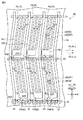
図1は、本実施形態の液晶表示装置を構成する液晶表示パネルPNLの構成及び等価回路を概略的に示す図である。 FIG. 1 is a diagram schematically showing a configuration and an equivalent circuit of a liquid crystal display panel PNL constituting the liquid crystal display device of the present embodiment.
すなわち、液晶表示パネルPNLは、アクティブマトリクスタイプの透過型であり、アレイ基板ARと、アレイ基板ARに対向配置された対向基板CTと、アレイ基板ARと対向基板CTとの間に保持された液晶層LQと、を備えている。アレイ基板ARと対向基板CTとは、これらの間に所定のセルギャップを形成した状態でシール材SEによって貼り合わせられている。図示した例では、シール材SEは、矩形枠状の閉ループ形状をなすように形成されている。液晶層LQは、シール材SEによって囲まれた内側でアレイ基板ARと対向基板CTとの間に保持されている。液晶表示パネルPNLは、シール材SEによって囲まれた内側に、画像を表示するアクティブエリアACTを備えている。アクティブエリアACTは、例えば、略長方形状であり、マトリクス状に配置された複数の画素PXによって構成されている。一例では、アクティブエリアACTは、第1方向Xに対して略平行な短辺TSHと、第2方向Yに対して略平行な長辺TLOと、を有している。なお、第1方向Xは、第2方向Yと直交している。また、液晶表示パネルPNL(あるいは、アレイ基板AR及び対向基板CT)も長方形状に形成され、第1方向Xに対して略平行な短辺LSHと、第2方向Yに対して略平行な長辺LLOと、を有している。 That is, the liquid crystal display panel PNL is an active matrix type transmissive type, and the liquid crystal held between the array substrate AR, the counter substrate CT disposed to face the array substrate AR, and the array substrate AR and the counter substrate CT. And a layer LQ. The array substrate AR and the counter substrate CT are bonded together with a sealant SE in a state where a predetermined cell gap is formed between them. In the illustrated example, the sealing material SE is formed to have a rectangular frame-shaped closed loop shape. The liquid crystal layer LQ is held between the array substrate AR and the counter substrate CT on the inner side surrounded by the sealing material SE. The liquid crystal display panel PNL includes an active area ACT that displays an image on the inner side surrounded by the seal material SE. The active area ACT has, for example, a substantially rectangular shape and includes a plurality of pixels PX arranged in a matrix. In one example, the active area ACT has a short side TSH substantially parallel to the first direction X and a long side TLO substantially parallel to the second direction Y. The first direction X is orthogonal to the second direction Y. The liquid crystal display panel PNL (or the array substrate AR and the counter substrate CT) is also formed in a rectangular shape, and has a short side LSH substantially parallel to the first direction X and a length substantially parallel to the second direction Y. Side LLO.
アレイ基板ARは、アクティブエリアACTにおいて、例えば、短辺TSHと平行な方向(あるいは第1方向X)に沿って延出したゲート配線G、長辺TLOと平行な方向(あるいは第2方向Y)に沿って延出したソース配線S、各画素PXにおいてゲート配線G及びソース配線Sと電気的に接続されたスイッチング素子SW、各画素PXにおいてスイッチング素子SWと電気的に接続された画素電極PE、コモン電位の共通電極CEなどを備えている。 In the active area ACT, the array substrate AR has, for example, a gate wiring G extending along a direction parallel to the short side TSH (or the first direction X) and a direction parallel to the long side TLO (or the second direction Y). A source line S extending along the line, a switching element SW electrically connected to the gate line G and the source line S in each pixel PX, a pixel electrode PE electrically connected to the switching element SW in each pixel PX, A common electrode CE having a common potential is provided.
なお、液晶表示パネルPNLの詳細な構成については後述するが、本実施形態の液晶表示パネルPNLは、主として横電界を利用するモードを適用可能に構成され、画素電極PE及び共通電極CEの双方がアレイ基板ARに備えられている。 Although a detailed configuration of the liquid crystal display panel PNL will be described later, the liquid crystal display panel PNL of the present embodiment is configured to be able to apply a mode that mainly uses a lateral electric field, and both the pixel electrode PE and the common electrode CE are provided. It is provided in the array substrate AR.
駆動ICチップ2及びフレキシブル・プリンテッド・サーキット(FPC)基板3などの液晶表示パネルPNLの駆動に必要な信号供給源は、アクティブエリアACTよりも外側の周辺エリアPRPに位置している。図示した例では、駆動ICチップ2及びFPC基板3は、対向基板CTの基板端部CTEよりも外側に延出したアレイ基板ARの実装部MTに実装されている。周辺エリアPRPは、アクティブエリアACTを囲むエリアであり、シール材SEが配置されるエリアを含み、矩形枠状に形成されている。
Signal supply sources necessary for driving the liquid crystal display panel PNL such as the driving IC chip 2 and the flexible printed circuit (FPC)
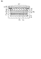
図2は、図1に示したアレイ基板ARにおける画素の構成例を対向基板CTの側から見た概略平面図である。ただし、図中には説明に必要な主要部のみを図示している。 FIG. 2 is a schematic plan view of a configuration example of pixels in the array substrate AR shown in FIG. 1 as viewed from the counter substrate CT side. However, only the main parts necessary for explanation are shown in the figure.
アレイ基板ARは、ゲート配線G1乃至G3、ソース配線S1乃至S4、スイッチング素子SW1乃至SW6、共通電極CE、画素電極PE1乃至PE6、第1配向膜AL1、などを備えている。 The array substrate AR includes gate lines G1 to G3, source lines S1 to S4, switching elements SW1 to SW6, a common electrode CE, pixel electrodes PE1 to PE6, a first alignment film AL1, and the like.
ゲート配線G1乃至G3は、第1方向Xに対して略平行に延出している。ソース配線S1乃至S4は、第2方向Yに対して略平行に延出し、ゲート配線G1乃至G3と交差している。なお、ゲート配線G1乃至G3及びソース配線S1乃至S4は、必ずしも直線的に延出していなくても良く、一部が屈曲していてもよい。これらのゲート配線G1乃至G3及びソース配線S1乃至S4は、画素PX1乃至PX6を区画している。ゲート配線G1乃至G3及びソース配線S1乃至S4は、例えば、モリブデン、クロム、タングステン、アルミニウム、銅、チタン、ニッケル、タンタル、銀あるいはこれらの合金によって形成されているが、特に限定されるものではなく、その他の金属や合金、またはこれらの積層膜で形成されていてもよい。 The gate wirings G1 to G3 extend substantially parallel to the first direction X. The source lines S1 to S4 extend substantially parallel to the second direction Y and intersect the gate lines G1 to G3. Note that the gate wirings G1 to G3 and the source wirings S1 to S4 do not necessarily extend linearly, and some of them may be bent. These gate lines G1 to G3 and source lines S1 to S4 partition the pixels PX1 to PX6. The gate wirings G1 to G3 and the source wirings S1 to S4 are made of, for example, molybdenum, chromium, tungsten, aluminum, copper, titanium, nickel, tantalum, silver, or alloys thereof, but are not particularly limited. , Other metals and alloys, or a laminated film thereof.
第1方向Xに並んだ画素PX1乃至PX3は互いに異なる色の色画素であり、また、画素PX4乃至PX6も互いに異なる色の色画素である。一例として、第2方向Yに並んだ画素PX1及びPX4は同一色の画素であり、例えば緑色(G)画素である。第2方向Yに並んだ画素PX2及びPX5は同一色の画素であり、例えば青色(B)画素である。第2方向Yに並んだ画素PX3及びPX6は同一色の画素であり、例えば赤色(R)画素である。 The pixels PX1 to PX3 arranged in the first direction X are different color pixels, and the pixels PX4 to PX6 are also different color pixels. As an example, the pixels PX1 and PX4 arranged in the second direction Y are pixels of the same color, for example, green (G) pixels. The pixels PX2 and PX5 arranged in the second direction Y are the same color pixels, for example, blue (B) pixels. The pixels PX3 and PX6 arranged in the second direction Y are the same color pixels, for example, red (R) pixels.
画素PX1はゲート配線G1及びゲート配線G2とソース配線S1及びソース配線S2とで規定され、画素PX2はゲート配線G1及びゲート配線G2とソース配線S2及びソース配線S3とで規定され、画素PX3はゲート配線G1及びゲート配線G2とソース配線S3及びソース配線S4とで規定されている。これらの画素PX1乃至PX3は、第2方向Yに対して時計回りに鋭角に交差する第1延出方向D1に延出している。各画素PX1乃至PX3の両側に位置するソース配線S1乃至S4は第1延出方向D1に延出している。 The pixel PX1 is defined by the gate wiring G1, the gate wiring G2, the source wiring S1, and the source wiring S2, the pixel PX2 is defined by the gate wiring G1, the gate wiring G2, the source wiring S2, and the source wiring S3, and the pixel PX3 is a gate. It is defined by the wiring G1, the gate wiring G2, the source wiring S3, and the source wiring S4. These pixels PX1 to PX3 extend in the first extending direction D1 that intersects the second direction Y clockwise at an acute angle. The source lines S1 to S4 located on both sides of each pixel PX1 to PX3 extend in the first extending direction D1.
画素PX4はゲート配線G2及びゲート配線G3とソース配線S1及びソース配線S2とで規定され、画素PX5はゲート配線G2及びゲート配線G3とソース配線S2及びソース配線S3とで規定され、画素PX6はゲート配線G2及びゲート配線G3とソース配線S3及びソース配線S4とで規定されている。これらの画素PX4乃至PX6は、第2方向Yに対して反時計回りに鋭角に交差する第2延出方向D2に延出している。各画素PX4乃至PX6の両側に位置するソース配線S1乃至S4は第2延出方向D2に延出している。なお、第2方向Yと第1延出方向D1とのなす角度θ1は、第2方向Yと第2延出方向D2とのなす角度θ2とほぼ同一であり、例えば5°〜15°程度である。 The pixel PX4 is defined by the gate line G2, the gate line G3, the source line S1, and the source line S2, the pixel PX5 is defined by the gate line G2, the gate line G3, the source line S2, and the source line S3, and the pixel PX6 is the gate. It is defined by the wiring G2, the gate wiring G3, the source wiring S3, and the source wiring S4. These pixels PX4 to PX6 extend in the second extending direction D2 that intersects the second direction Y counterclockwise at an acute angle. The source lines S1 to S4 located on both sides of each pixel PX4 to PX6 extend in the second extending direction D2. The angle θ1 formed by the second direction Y and the first extending direction D1 is substantially the same as the angle θ2 formed by the second direction Y and the second extending direction D2, and is, for example, about 5 ° to 15 °. is there.
共通電極CEは、アレイ基板ARの略全域に亘って延在し、画素PX1乃至PX6に共通に形成されている。すなわち、共通電極CEは、ゲート配線G1乃至G3の上方を跨いで第2方向Yに延在するとともに、ソース配線S1乃至S4の上方を跨いで第1方向Xに延在し、画素PX1乃至PX6のそれぞれに配置されている。 The common electrode CE extends over substantially the entire area of the array substrate AR and is formed in common for the pixels PX1 to PX6. That is, the common electrode CE extends in the second direction Y over the gate lines G1 to G3, and extends in the first direction X over the source lines S1 to S4, and the pixels PX1 to PX6. Are arranged in each.
画素PX1には、スイッチング素子SW1及び画素電極PE1が配置されている。スイッチング素子SW1は、ゲート配線G2及びソース配線S1と電気的に接続されている。画素電極PE1は、ソース配線S1とソース配線S2との間に位置し、スイッチング素子SW1と電気的に接続されている。画素PX2には、スイッチング素子SW2及び画素電極PE2が配置されている。スイッチング素子SW2は、ゲート配線G2及びソース配線S2と電気的に接続されている。画素電極PE2は、ソース配線S2とソース配線S3との間に位置し、スイッチング素子SW2と電気的に接続されている。画素PX3には、スイッチング素子SW3及び画素電極PE3が配置されている。スイッチング素子SW3は、ゲート配線G2及びソース配線S3と電気的に接続されている。画素電極PE3は、ソース配線S3とソース配線S4との間に位置し、スイッチング素子SW3と電気的に接続されている。 In the pixel PX1, the switching element SW1 and the pixel electrode PE1 are arranged. The switching element SW1 is electrically connected to the gate line G2 and the source line S1. The pixel electrode PE1 is located between the source line S1 and the source line S2, and is electrically connected to the switching element SW1. In the pixel PX2, a switching element SW2 and a pixel electrode PE2 are arranged. The switching element SW2 is electrically connected to the gate line G2 and the source line S2. The pixel electrode PE2 is located between the source line S2 and the source line S3, and is electrically connected to the switching element SW2. In the pixel PX3, a switching element SW3 and a pixel electrode PE3 are arranged. The switching element SW3 is electrically connected to the gate line G2 and the source line S3. The pixel electrode PE3 is located between the source line S3 and the source line S4, and is electrically connected to the switching element SW3.
同様に、画素PX4には、ゲート配線G3及びソース配線S1と電気的に接続されたスイッチング素子SW4、及び、スイッチング素子SW4と電気的に接続された画素電極PE4が配置されている。画素PX5には、ゲート配線G3及びソース配線S2と電気的に接続されたスイッチング素子SW5、及び、スイッチング素子SW5と電気的に接続された画素電極PE5が配置されている。画素PX6には、ゲート配線G3及びソース配線S3と電気的に接続されたスイッチング素子SW6、及び、スイッチング素子SW6と電気的に接続された画素電極PE6が配置されている。 Similarly, in the pixel PX4, a switching element SW4 electrically connected to the gate line G3 and the source line S1, and a pixel electrode PE4 electrically connected to the switching element SW4 are arranged. In the pixel PX5, a switching element SW5 electrically connected to the gate line G3 and the source line S2 and a pixel electrode PE5 electrically connected to the switching element SW5 are arranged. In the pixel PX6, a switching element SW6 electrically connected to the gate line G3 and the source line S3, and a pixel electrode PE6 electrically connected to the switching element SW6 are arranged.
スイッチング素子SW1乃至SW6は、例えば薄膜トランジスタ(TFT)である。このようなスイッチング素子SW1乃至SW6は、例えば、ポリシリコン(p−Si)、アモルファスシリコン(a−Si)、有機物半導体、または酸化物半導体等によって形成される半導体層を備えている。 The switching elements SW1 to SW6 are, for example, thin film transistors (TFTs). Such switching elements SW1 to SW6 include a semiconductor layer formed of, for example, polysilicon (p-Si), amorphous silicon (a-Si), an organic semiconductor, or an oxide semiconductor.
画素電極PE1乃至PE6は、それぞれ共通電極CEの上方に位置している。画素電極PE1乃至PE3は、それぞれ第1延出方向D1に延出した画素形状に対応した島状に形成されている。また、画素電極PE1乃至PE3は、それぞれ第1延出方向D1に延出した複数のスリットSLAを有している。画素電極PE4乃至PE6は、それぞれ第2延出方向D2に延出した画素形状に対応した島状に形成されている。また、画素電極PE4乃至PE6は、それぞれ第2延出方向D2に延出した複数のスリットSLBを有している。各スリットSLA及びSLBは、いずれも共通電極CEと向かい合っている。図示した例では、画素電極PE1乃至PE3は各々2本のスリットSLAを有し、画素電極PE4乃至PE6各々2本のスリットSLBを有している。1つの画素電極が有するスリットの本数は、特に限定されるものではなく、1本でも良いし、3本以上であってもよい。 The pixel electrodes PE1 to PE6 are respectively located above the common electrode CE. The pixel electrodes PE1 to PE3 are each formed in an island shape corresponding to the pixel shape extending in the first extending direction D1. Further, the pixel electrodes PE1 to PE3 each have a plurality of slits SLA extending in the first extending direction D1. The pixel electrodes PE4 to PE6 are each formed in an island shape corresponding to the pixel shape extending in the second extending direction D2. Further, the pixel electrodes PE4 to PE6 each have a plurality of slits SLB extending in the second extending direction D2. Each of the slits SLA and SLB faces the common electrode CE. In the illustrated example, each of the pixel electrodes PE1 to PE3 has two slits SLA, and each of the pixel electrodes PE4 to PE6 has two slits SLB. The number of slits included in one pixel electrode is not particularly limited, and may be one or three or more.
第1配向膜AL1は、スリットSLAの長軸(図2に示した例では第1延出方向D1)及びスリットSLBの長軸(図2に示した例では第2延出方向D2)に対して45°以上の鋭角に交差する方向に沿って配向処理されている。第1配向膜AL1の配向方向R1は、第1方向Xに対して略平行な方向であり、第1延出方向D1あるいは第2延出方向D2に対して90°未満、例えば75°〜85°の角度をもって交差する方向である。 The first alignment film AL1 is formed with respect to the long axis of the slit SLA (first extending direction D1 in the example shown in FIG. 2) and the long axis of the slit SLB (second extending direction D2 in the example shown in FIG. 2). Orientation treatment is performed along a direction intersecting an acute angle of 45 ° or more. The alignment direction R1 of the first alignment film AL1 is a direction substantially parallel to the first direction X and is less than 90 °, for example, 75 ° to 85 with respect to the first extending direction D1 or the second extending direction D2. Crossing direction with an angle of °.
図3は、図2に示した画素PX1乃至PX3を含む液晶表示パネルPNLの構成を概略的に示す断面図である。 FIG. 3 is a cross-sectional view schematically showing the configuration of the liquid crystal display panel PNL including the pixels PX1 to PX3 shown in FIG.
液晶表示パネルPNLは、アレイ基板AR、対向基板CT、及び液晶層LQを備えている。さらに、第1光学素子OD1及び第2光学素子OD2は、液晶表示パネルPNLの外面に配置されている。 The liquid crystal display panel PNL includes an array substrate AR, a counter substrate CT, and a liquid crystal layer LQ. Further, the first optical element OD1 and the second optical element OD2 are disposed on the outer surface of the liquid crystal display panel PNL.
アレイ基板ARは、第1絶縁基板10、第1絶縁膜11、共通電極CE、第2絶縁膜12、画素電極PE1乃至PE3、第1配向膜AL1等を備えている。第1絶縁基板10は、ガラス、樹脂等の光透過性及び絶縁性を有する材料によって形成されている。
The array substrate AR includes a first insulating
第1絶縁膜11は、第1絶縁基板10の上に形成されている。また、図示しないゲート配線やソース配線、スイッチング素子などは、第1絶縁基板10と第1絶縁膜11との間に形成されている。
The first insulating
共通電極CEは、第1絶縁膜11の上に形成されている。共通電極CEは、透明な導電材料、例えば、インジウム・ティン・オキサイド(ITO)やインジウム・ジンク・オキサイド(IZO)などによって形成されている。共通電極CEは、第2絶縁膜12によって覆われている。
The common electrode CE is formed on the first insulating
画素電極PE1乃至PE3は、第2絶縁膜12の上に形成され、共通電極CEと対向している。画素電極PE1乃至PE3には、それぞれスリットSLAが形成されている。画素電極PE1乃至PE3は、透明な導電材料、例えば、ITOやIZOなどによって形成されている。
The pixel electrodes PE1 to PE3 are formed on the second insulating
第1配向膜AL1は、画素電極PE1乃至PE3を覆うとともに、第2絶縁膜12の上にも形成されている。第1配向膜AL1は、水平配向性を示す材料によって形成され、アレイ基板ARの液晶層LQに接する面に配置されている。
The first alignment film AL1 covers the pixel electrodes PE1 to PE3 and is also formed on the second insulating
一方、対向基板CTは、第2絶縁基板20、遮光層BM、カラーフィルタCF1、カラーフィルタCF2、カラーフィルタCF3、オーバーコート層OC、第2配向膜AL2などを備えている。第2絶縁基板20は、ガラス、樹脂等の光透過性及び絶縁性を有する材料によって形成されている。
On the other hand, the counter substrate CT includes a second insulating
遮光層BMは、第2絶縁基板20のアレイ基板ARに対向する内面に形成されている。遮光層BMは、光透過率が低く反射率が低い、黒色の樹脂材料や遮光性の金属材料によって形成される。
The light shielding layer BM is formed on the inner surface of the second insulating
カラーフィルタCF1乃至CF3のそれぞれは、第2絶縁基板20の内面に形成されている。カラーフィルタCF1は、緑色に着色された樹脂材料によって形成されている。カラーフィルタCF2は、青色に着色された樹脂材料によって形成されている。カラーフィルタCF3は、赤色に着色された樹脂材料によって形成されている。なお、これらのカラーフィルタCF1乃至CF3とは異なる色(例えば、透明、白色など)のカラーフィルタがさらに追加されても良い。
Each of the color filters CF1 to CF3 is formed on the inner surface of the second insulating
オーバーコート層OCは、カラーフィルタCF1乃至CF3を覆っている。オーバーコート層OCは、例えば透明な樹脂材料によって形成される。 The overcoat layer OC covers the color filters CF1 to CF3. The overcoat layer OC is formed of, for example, a transparent resin material.
第2配向膜AL2は、オーバーコート層OCを覆っている。第2配向膜AL2は、水平配向性を示す材料によって形成され、対向基板CTの液晶層LQに接する面に配置されている。このような第1配向膜AL1及び第2配向膜AL2は、液晶層LQの液晶分子を初期配向させるための配向処理がなされている。第1配向膜AL1の配向方向R1は、図2に示した通り、第1方向Xと平行である。第2配向膜AL2の配向方向R2は、配向方向R1と平行かつ同じ向きである。配向処理としては、例えば、ラビング処理や光配向処理等が挙げられる。 The second alignment film AL2 covers the overcoat layer OC. The second alignment film AL2 is formed of a material exhibiting horizontal alignment, and is disposed on the surface in contact with the liquid crystal layer LQ of the counter substrate CT. Such first alignment film AL1 and second alignment film AL2 are subjected to alignment treatment for initial alignment of the liquid crystal molecules of the liquid crystal layer LQ. The alignment direction R1 of the first alignment film AL1 is parallel to the first direction X as shown in FIG. The alignment direction R2 of the second alignment film AL2 is parallel to and in the same direction as the alignment direction R1. Examples of the alignment treatment include rubbing treatment and optical alignment treatment.
液晶層LQは、アレイ基板ARの第1配向膜AL1と対向基板CTの第2配向膜AL2との間に封入された液晶分子LMを含んでいる。このような液晶層LQは、誘電率異方性が負(ネガ型)の液晶組成物によって構成されている。液晶分子LMは、第1配向膜AL1及び第2配向膜AL2から配向規制力を受け、第1配向膜AL1及び第2配向膜AL2と液晶層LQとの界面に対して略平行に初期配向している。図2に示した例では、液晶分子LMの初期配向方向は、第1方向Xに平行である。 The liquid crystal layer LQ includes liquid crystal molecules LM sealed between the first alignment film AL1 of the array substrate AR and the second alignment film AL2 of the counter substrate CT. Such a liquid crystal layer LQ is composed of a liquid crystal composition having a negative (negative) dielectric anisotropy. The liquid crystal molecules LM receive an alignment regulating force from the first alignment film AL1 and the second alignment film AL2, and are initially aligned substantially parallel to the interface between the first alignment film AL1, the second alignment film AL2, and the liquid crystal layer LQ. ing. In the example shown in FIG. 2, the initial alignment direction of the liquid crystal molecules LM is parallel to the first direction X.
第1光学素子OD1は、アレイ基板ARの表面に接着されている。第1光学素子OD1は、位相差板RE及び第1偏光板PL1を含んでいる。第2光学素子OD2は、対向基板CTの表面に接着されており、第2偏光板PL2を含んでいる。第1光学素子OD1及び第2光学素子OD2は、本実施形態に限定されず、他の機能層を含んでいてもよい。 The first optical element OD1 is bonded to the surface of the array substrate AR. The first optical element OD1 includes a retardation plate RE and a first polarizing plate PL1. The second optical element OD2 is bonded to the surface of the counter substrate CT and includes a second polarizing plate PL2. The first optical element OD1 and the second optical element OD2 are not limited to the present embodiment, and may include other functional layers.
このような構成の液晶表示パネルPNLに対して、第1光学素子OD1に対向する位置にバックライトユニットBLが配置されている。バックライトユニットBLとしては、種々の形態が適用可能であるが、詳細な構造については説明を省略する。 The backlight unit BL is arranged at a position facing the first optical element OD1 with respect to the liquid crystal display panel PNL having such a configuration. Although various forms are applicable as the backlight unit BL, the description of the detailed structure is omitted.
図4は、液晶表示パネルPNL及びカバー部材CGを含む液晶表示装置の構成を概略的に示す断面図である。 FIG. 4 is a cross-sectional view schematically showing the configuration of the liquid crystal display device including the liquid crystal display panel PNL and the cover member CG.
液晶表示装置は、箱型の筐体FRの中に、バックライトユニットBL、液晶表示パネルPNL、第1光学素子OD1の位相差板RE及び第1偏光板PL1、第2光学素子OD2の第2偏光板PL2、及び紫外線硬化樹脂UCを収容している。 The liquid crystal display device includes a backlight unit BL, a liquid crystal display panel PNL, a retardation plate RE of the first optical element OD1, a first polarizing plate PL1, and a second optical element OD2 in a box-shaped casing FR. The polarizing plate PL2 and the ultraviolet curable resin UC are accommodated.
カバー部材CGは、液晶表示パネルPNLの対向基板CTと対向する側に配置されている。カバー部材CGは、光透過性を有する、ガラスや樹脂等によって形成されている。カバー部材CGは、筐体FRに接着されるなどして固定されている。一例では、カバー部材CGは、液晶表示パネルPNLと対向する側に遮光層SHを備えている。遮光層SHは、アクティブエリアACTを規定するとともに、アクティブエリアACTよりも外側の領域を遮光する。 The cover member CG is disposed on the side facing the counter substrate CT of the liquid crystal display panel PNL. The cover member CG is formed of glass, resin, or the like having optical transparency. The cover member CG is fixed by being adhered to the housing FR. In one example, the cover member CG includes a light shielding layer SH on the side facing the liquid crystal display panel PNL. The light shielding layer SH defines the active area ACT and shields an area outside the active area ACT.
バックライトユニットBLは、筐体FRの底面に配置されている。液晶表示パネルPNLは、バックライトユニットBLに対向している。位相差板REは、アレイ基板ARのバックライトユニットBLに対向する表面ARaに接着されている。第1偏光板PL1は、位相差板REに貼合されている。第2偏光板PL2は、対向基板CTのカバー部材CGに対向する表面CTaに接着されている。これらの位相差板RE、第1偏光板PL1、及び、第2偏光板PL2は、いずれもアクティブエリアACTの全体に亘って配置されている。 The backlight unit BL is disposed on the bottom surface of the housing FR. The liquid crystal display panel PNL faces the backlight unit BL. The phase difference plate RE is bonded to the surface ARa facing the backlight unit BL of the array substrate AR. The first polarizing plate PL1 is bonded to the retardation plate RE. The second polarizing plate PL2 is bonded to the surface CTa facing the cover member CG of the counter substrate CT. The retardation plate RE, the first polarizing plate PL1, and the second polarizing plate PL2 are all disposed over the entire active area ACT.
紫外線硬化樹脂UCは、第2偏光板PL2とカバー部材CGとを接着している。紫外線硬化樹脂UCは、アクティブエリアACTの全体に亘って配置されている。紫外線硬化樹脂UCをアクティブエリアACTの全体に亘って配置するのに必要な量を塗布した際、一部の紫外線硬化樹脂UCは、アクティブエリアACTよりも外側に広がる。近年では、アクティブエリアACTの外側の額縁幅が小さくなる傾向があるため、紫外線硬化樹脂UCを第2偏光板PL2の表面HFのみに留めることが困難となりつつある。このため、図示した例では、紫外線硬化樹脂UCは、第2偏光板PL2の表面HF及び側面LFに接触している。さらに、紫外線硬化樹脂UCは、第2偏光板PL2から露出した対向基板CTの一部の表面CTaにも接触している。 The ultraviolet curable resin UC bonds the second polarizing plate PL2 and the cover member CG. The ultraviolet curable resin UC is disposed over the entire active area ACT. When an amount necessary for disposing the ultraviolet curable resin UC over the entire active area ACT is applied, a part of the ultraviolet curable resin UC spreads outside the active area ACT. In recent years, since the frame width outside the active area ACT tends to be small, it is becoming difficult to keep the ultraviolet curable resin UC only on the surface HF of the second polarizing plate PL2. For this reason, in the illustrated example, the ultraviolet curable resin UC is in contact with the surface HF and the side surface LF of the second polarizing plate PL2. Further, the ultraviolet curable resin UC is also in contact with a part of the surface CTa of the counter substrate CT exposed from the second polarizing plate PL2.
位相差板REは、例えば、液晶表示装置の視野角補償等のために備えられる。一般に、位相差板REは、液晶表示パネルPNLと第1偏光板PL1との間、及び、液晶表示パネルPNLと第2偏光板PL2との間の少なくとも一方に配置される。本実施形態では、位相差板REは、液晶表示パネルPNLと第1偏光板PL1との間のみに配置される。このため、位相差板REは、紫外線硬化樹脂UCと接触することはない。なお、位相差板REの位相差値や遅相軸方向は特に限定されるものではなく、液晶表示パネルPNLの性能や第1偏光板PL1の第1吸収軸AB1の方向に合わせて適宜選択できる。一例では、このような位相差板REは、第1偏光板PL1と予め一体化され、その遅相軸と第1偏光板PL1の第1吸収軸AB1とが所定のなす角度で交差するように設定されている。 The phase difference plate RE is provided, for example, for viewing angle compensation of a liquid crystal display device. In general, the retardation plate RE is disposed between the liquid crystal display panel PNL and the first polarizing plate PL1 and at least one between the liquid crystal display panel PNL and the second polarizing plate PL2. In the present embodiment, the retardation film RE is disposed only between the liquid crystal display panel PNL and the first polarizing plate PL1. For this reason, the phase difference plate RE does not come into contact with the ultraviolet curable resin UC. The phase difference value and the slow axis direction of the retardation plate RE are not particularly limited, and can be appropriately selected according to the performance of the liquid crystal display panel PNL and the direction of the first absorption axis AB1 of the first polarizing plate PL1. . In one example, such a retardation plate RE is integrated with the first polarizing plate PL1 in advance, and the slow axis thereof intersects the first absorption axis AB1 of the first polarizing plate PL1 at a predetermined angle. Is set.
次に、本実施形態の液晶表示装置の使用形態について、図5に一例を挙げて説明する。 Next, the usage pattern of the liquid crystal display device of this embodiment will be described with reference to FIG.
図5は、第1偏光板PL1の第1吸収軸AB1の方向、液晶分子LMの初期配向方向、第2偏光板PL2の第2吸収軸AB2の方向、及び偏光サングラスSGの第3吸収軸AB3の方向の相互関係を概略的に示した図である。 FIG. 5 shows the direction of the first absorption axis AB1 of the first polarizing plate PL1, the initial alignment direction of the liquid crystal molecules LM, the direction of the second absorption axis AB2 of the second polarizing plate PL2, and the third absorption axis AB3 of the polarizing sunglasses SG. It is the figure which showed the mutual relationship of the direction of.
液晶表示装置は、使用者によってアクティブエリアACTが縦長になるように把持されている。また、使用者は、正面からアクティブエリアACTを見ている。すなわち、アクティブエリアACTの短辺TSHが水平方向と略平行になり、長辺TLOが鉛直方向と略平行になる。同様に、第1偏光板PL1、液晶表示パネルPNL、第2偏光板PL2、及びカバー部材CGは、いずれも水平方向と略平行な短辺と、鉛直方向と略平行な長辺とを有している。なお、図1で示したように、本実施形態において、ゲート配線Gは、アクティブエリアACTの短辺TSHに対して略平行に延出している。また、ソース配線Sは、アクティブエリアACTの長辺TLOに対して略平行に延出している。従って、液晶表示装置の使用時、水平方向とはゲート配線Gの延出方向(あるいは第1方向X)に相当し、鉛直方向とはソース配線Sの延出方向(あるいは第2方向Y)に相当する。なお、第1偏光板PL1、液晶表示パネルPNL、第2偏光板PL2、及びカバー部材CGを貫通する破線の矢印は、使用者が視認する液晶表示装置からの出射光LTの経路を示している。 The liquid crystal display device is held by the user so that the active area ACT is vertically long. In addition, the user looks at the active area ACT from the front. That is, the short side TSH of the active area ACT is substantially parallel to the horizontal direction, and the long side TLO is substantially parallel to the vertical direction. Similarly, each of the first polarizing plate PL1, the liquid crystal display panel PNL, the second polarizing plate PL2, and the cover member CG has a short side substantially parallel to the horizontal direction and a long side substantially parallel to the vertical direction. ing. As shown in FIG. 1, in the present embodiment, the gate wiring G extends substantially in parallel to the short side TSH of the active area ACT. The source line S extends substantially parallel to the long side TLO of the active area ACT. Accordingly, when the liquid crystal display device is used, the horizontal direction corresponds to the extending direction (or the first direction X) of the gate wiring G, and the vertical direction is the extending direction (or the second direction Y) of the source wiring S. Equivalent to. In addition, the broken-line arrow which penetrates 1st polarizing plate PL1, liquid crystal display panel PNL, 2nd polarizing plate PL2, and cover member CG has shown the path | route of the emitted light LT from the liquid crystal display device which a user visually recognizes. .
第1偏光板PL1の第1吸収軸AB1は、第2方向Yと平行である。液晶分子LMの初期配向方向は、第1方向Xと平行である。第2偏光板PL2の第2吸収軸AB2は、第1吸収軸AB1と直交する位置関係にあり、第1方向Xと平行である。すなわち、第1偏光板PL1と第2偏光板PL2は、クロスニコルの位置関係で配置されている。また、第2吸収軸AB2は、アクティブエリアACTの短辺TSHと平行であり、また、ゲート配線Gの延出方向とも平行である。液晶分子LMの初期配向方向は、第2吸収軸AB2と平行である。 The first absorption axis AB1 of the first polarizing plate PL1 is parallel to the second direction Y. The initial alignment direction of the liquid crystal molecules LM is parallel to the first direction X. The second absorption axis AB2 of the second polarizing plate PL2 is in a positional relationship orthogonal to the first absorption axis AB1, and is parallel to the first direction X. That is, the first polarizing plate PL1 and the second polarizing plate PL2 are arranged in a crossed Nicols positional relationship. The second absorption axis AB2 is parallel to the short side TSH of the active area ACT, and is also parallel to the extending direction of the gate wiring G. The initial alignment direction of the liquid crystal molecules LM is parallel to the second absorption axis AB2.
一方、偏光サングラスSGの第3吸収軸AB3は、太陽光の水面等での反射光を遮断するために、水平方向(あるいは第1方向X)と平行である。カバー部材CGを通過して液晶表示装置の外部へ出射された出射光LTは、第2吸収軸AB2と略垂直な直線偏光である。従って、このような出射光LTの偏光方向は、偏光サングラスSGの第3吸収軸AB3と略直交する。このため、液晶表示装置から出射された出射光LTは、偏光サングラスSGを通して視認される。 On the other hand, the third absorption axis AB3 of the polarized sunglasses SG is parallel to the horizontal direction (or the first direction X) in order to block the reflected light on the water surface of sunlight. The outgoing light LT that passes through the cover member CG and is emitted to the outside of the liquid crystal display device is linearly polarized light that is substantially perpendicular to the second absorption axis AB2. Therefore, the polarization direction of such emitted light LT is substantially orthogonal to the third absorption axis AB3 of the polarized sunglasses SG. For this reason, the emitted light LT emitted from the liquid crystal display device is visually recognized through the polarized sunglasses SG.
以下に、上記構成の液晶表示装置における動作について説明する。 The operation of the liquid crystal display device having the above configuration will be described below.
画素電極PEと共通電極CEとの間に電位差を形成するような電圧が印加されていないOFF時においては、液晶層LQに電圧が印加されていない。つまり、画素電極PEと共通電極CEとの間には、電界が形成されていない。このため、液晶層LQに含まれる液晶分子LMは、図2に実線で示したように、第1配向膜AL1及び第2配向膜AL2の配向規制力によりX−Y平面内において第1方向Xに初期配向している。 At the time of OFF when a voltage that forms a potential difference is not applied between the pixel electrode PE and the common electrode CE, no voltage is applied to the liquid crystal layer LQ. That is, no electric field is formed between the pixel electrode PE and the common electrode CE. Therefore, the liquid crystal molecules LM included in the liquid crystal layer LQ are aligned in the first direction X in the XY plane by the alignment regulating force of the first alignment film AL1 and the second alignment film AL2, as shown by the solid line in FIG. Is initially oriented.
OFF時には、バックライトユニットBLからのバックライト光の一部は、第1偏光板PL1を透過し、液晶表示パネルPNLに入射する。このとき、液晶表示パネルPNLに入射する光は、例えば第1偏光板PL1の第1吸収軸AB1と直交する直線偏光である。このような直線偏光の偏光状態は、OFF時の液晶表示パネルPNLを通過した際にほとんど変化しない。このため、液晶表示パネルPNLを透過した直線偏光のほとんどが、第2偏光板PL2によって吸収される(黒表示)。 When OFF, a part of the backlight light from the backlight unit BL passes through the first polarizing plate PL1 and enters the liquid crystal display panel PNL. At this time, the light incident on the liquid crystal display panel PNL is, for example, linearly polarized light orthogonal to the first absorption axis AB1 of the first polarizing plate PL1. The polarization state of such linearly polarized light hardly changes when it passes through the liquid crystal display panel PNL when OFF. For this reason, most of the linearly polarized light transmitted through the liquid crystal display panel PNL is absorbed by the second polarizing plate PL2 (black display).
一方、画素電極PEと共通電極CEとの間に電位差を形成するような電圧が印加されたON時においては、液晶層LQに電圧が印加される。つまり、画素電極PEと共通電極CEとの間には、X−Y平面に対して略平行な横電界(あるいはフリンジ電界)が形成される。このため、液晶分子LMは、図2に破線で示したように、X−Y平面内において、初期配向方向とは異なる方位に配向する。ネガ型の液晶材料においては、例えば画素PX3の液晶分子LMは、X−Y平面内において、フリンジ電界と略垂直な方向に配向するように反時計回りに回転し、画素PX6の液晶分子LMは、X−Y平面内において、フリンジ電界と略垂直な方向に配向するように時計回りに回転する。このとき、液晶分子LMは、電界の大きさに応じた方向に配向する。 On the other hand, when the voltage that forms a potential difference is applied between the pixel electrode PE and the common electrode CE, the voltage is applied to the liquid crystal layer LQ. That is, a lateral electric field (or fringe electric field) substantially parallel to the XY plane is formed between the pixel electrode PE and the common electrode CE. For this reason, the liquid crystal molecules LM are aligned in an azimuth different from the initial alignment direction in the XY plane, as indicated by a broken line in FIG. In the negative liquid crystal material, for example, the liquid crystal molecules LM of the pixel PX3 rotate counterclockwise so as to be aligned in a direction substantially perpendicular to the fringe electric field in the XY plane, and the liquid crystal molecules LM of the pixel PX6 are , Rotate clockwise in the XY plane so as to be oriented in a direction substantially perpendicular to the fringe electric field. At this time, the liquid crystal molecules LM are aligned in a direction corresponding to the magnitude of the electric field.
ON時には、第1偏光板PL1の第1吸収軸AB1と直交する直線偏光は、液晶表示パネルPNLに入射し、その偏光状態は、液晶層LQを通過する際に液晶分子LMの配向状態に応じて変化する。このため、ON時においては、液晶層LQを通過した少なくとも一部の光は、第2偏光板PL2を透過する(白表示)。 When ON, linearly polarized light orthogonal to the first absorption axis AB1 of the first polarizing plate PL1 is incident on the liquid crystal display panel PNL, and the polarization state depends on the alignment state of the liquid crystal molecules LM when passing through the liquid crystal layer LQ. Change. For this reason, at the time of ON, at least a part of the light that has passed through the liquid crystal layer LQ is transmitted through the second polarizing plate PL2 (white display).
このような構成により、ノーマリーブラックモードが実現される。 With such a configuration, a normally black mode is realized.
図2を参照して説明した構成の液晶表示装置では、第2方向Yに隣接する画素(例えば、画素PX1と画素PX4)は、同一色を表示する一方で、それぞれのスリットの延出方向が異なる画素電極を備えている。このため、第2方向Yに隣接する画素の液晶分子LMは、ON時にはそれぞれ異なる方向に配向する。つまり、第2方向Yに隣接し同一色を表示する画素は、疑似的に2種類のドメインを形成する。このような液晶表示装置は、奇数行目の画素と偶数行目の画素とで互いに視野角を補償するため、広視野角化が可能となる。 In the liquid crystal display device having the configuration described with reference to FIG. 2, the pixels adjacent to the second direction Y (for example, the pixel PX1 and the pixel PX4) display the same color, but the extending direction of each slit is Different pixel electrodes are provided. For this reason, the liquid crystal molecules LM of the pixels adjacent in the second direction Y are aligned in different directions when turned on. That is, pixels adjacent to the second direction Y and displaying the same color form two types of domains in a pseudo manner. In such a liquid crystal display device, since the viewing angle is compensated for between the odd-numbered pixels and the even-numbered pixels, the viewing angle can be increased.
なお、本実施形態において、アレイ基板ARと第1偏光板PL1との間に配置された位相差板REは、例えば、視野角補償フィルムとして機能する。すなわち、位相差板REは、OFF時の黒表示、あるいは、ON時の白表示の際に、液晶表示装置を正面方向から観察した場合に限らず、液晶表示装置を斜め方向から観察した場合であっても、液晶表示パネルPNLを透過した光に対して適度に位相差を付与し、見栄えの差異を補償している。 In the present embodiment, the retardation plate RE disposed between the array substrate AR and the first polarizing plate PL1 functions as a viewing angle compensation film, for example. That is, the phase difference plate RE is not limited to the case where the liquid crystal display device is observed from the front direction during black display when OFF or white display when ON, but when the liquid crystal display device is observed from an oblique direction. Even in such a case, an appropriate phase difference is given to the light transmitted through the liquid crystal display panel PNL to compensate for the difference in appearance.
以上のように、本実施形態によれば、位相差板REがアレイ基板ARの表面に接着される一方で、対向基板CTの表面に接着された第2偏光板PL2は紫外線硬化樹脂UCによってカバー部材CGと接着されている。このため、位相差板REは、紫外線硬化樹脂UCが塗布されてから硬化するまでの過程において、紫外線硬化樹脂原料に接触する恐れがない。したがって、位相差板REの紫外線硬化樹脂原料による変質あるいは破損を抑制することが可能となる。これにより、信頼性の低下を抑制することが可能な液晶表示装置を提供できる。発明者は、本実施形態の構成の液晶表示装置について、−40℃から+85℃まで温度を急変させる温度急変試験を250サイクル行ったところ、位相差板REの変質及び破損が発生していないことを確認した。 As described above, according to the present embodiment, the retardation film RE is bonded to the surface of the array substrate AR, while the second polarizing plate PL2 bonded to the surface of the counter substrate CT is covered with the ultraviolet curable resin UC. It is bonded to the member CG. For this reason, the retardation film RE is not likely to come into contact with the ultraviolet curable resin raw material in the process from application of the ultraviolet curable resin UC to curing. Therefore, it is possible to suppress the deterioration or breakage of the retardation film RE due to the ultraviolet curable resin material. Thereby, the liquid crystal display device which can suppress the fall of reliability can be provided. The inventor conducted 250 cycles of the temperature sudden change test for suddenly changing the temperature from −40 ° C. to + 85 ° C. with respect to the liquid crystal display device having the configuration of the present embodiment. It was confirmed.
また、本実施形態によれば、位相差板REが紫外線硬化樹脂原料と接触しないため、耐薬品性の高い位相差板REを使用する必要がない。従って、位相差板REの材料選択の自由度を向上することが可能となる。また、紫外線硬化樹脂UCについても、位相差板REの耐薬品性を考慮することなく、材料を選択できるため、材料選択の自由度を向上することが可能となる。さらには、位相差板RE及び紫外線硬化樹脂UCの材料選択の自由度が向上したことにより、より安価な材料の選択が可能となり、液晶表示装置のコストを削減することが可能となる。 Moreover, according to this embodiment, since the phase difference plate RE does not contact the ultraviolet curable resin material, it is not necessary to use the phase difference plate RE having high chemical resistance. Therefore, it is possible to improve the degree of freedom in selecting the material for the retardation plate RE. Moreover, since the material can be selected for the ultraviolet curable resin UC without considering the chemical resistance of the retardation plate RE, the degree of freedom in selecting the material can be improved. Furthermore, since the degree of freedom in selecting the material for the retardation plate RE and the ultraviolet curable resin UC is improved, it is possible to select a cheaper material and reduce the cost of the liquid crystal display device.
さらに、偏光サングラスSGの第3吸収軸AB3は、第2偏光板PL2の第2吸収軸AB2と略平行になる。このため、本実施形態によれば、使用者は偏光サングラスSGを掛けた状態であっても、液晶表示装置の表示画面を視認することができる。すなわち、偏光サングラス対応の液晶表示装置を提供することができる。 Further, the third absorption axis AB3 of the polarized sunglasses SG is substantially parallel to the second absorption axis AB2 of the second polarizing plate PL2. For this reason, according to the present embodiment, the user can visually recognize the display screen of the liquid crystal display device even when the user wears the polarized sunglasses SG. That is, a liquid crystal display device compatible with polarized sunglasses can be provided.
次に、本実施形態の変形例について説明する。 Next, a modification of this embodiment will be described.
図6は、液晶表示パネルPNL及びカバー部材CGを含む液晶表示装置の他の構成を概略的に示す断面図である。 FIG. 6 is a cross-sectional view schematically showing another configuration of the liquid crystal display device including the liquid crystal display panel PNL and the cover member CG.
ここに示した変形例は、図4に示した実施形態と比較して、カバー部材CGが液晶表示パネルPNLに対向する面にタッチセンサTPを備えている点で相違している。なお、他の構成については、図4に示した実施形態と同一であり、同一の参照符号を付して説明を省略する。 The modification shown here is different from the embodiment shown in FIG. 4 in that the cover member CG includes a touch sensor TP on the surface facing the liquid crystal display panel PNL. In addition, about another structure, it is the same as embodiment shown in FIG. 4, The same referential mark is attached | subjected and description is abbreviate | omitted.
すなわち、カバー部材CGは、支持体SP及びタッチセンサTPを備えている。支持体SPは、光透過性を有するガラスや樹脂等によって形成されている。タッチセンサTPは、支持体SPの液晶表示パネルPNLと対向する面に形成されている。このようなカバー部材CGは、紫外線硬化樹脂UCにより、第2偏光板PL2に接着されている。 That is, the cover member CG includes a support SP and a touch sensor TP. The support SP is made of light-transmitting glass or resin. The touch sensor TP is formed on the surface of the support SP that faces the liquid crystal display panel PNL. Such a cover member CG is bonded to the second polarizing plate PL2 with an ultraviolet curable resin UC.
このような変形例においても、上記したのと同様の効果が得られる。 Even in such a modification, the same effect as described above can be obtained.
なお、本実施形態においては、第1電極として共通電極CEが配置され、スリットを有する第2電極として画素電極PEが配置された例について説明したが、第1電極として画素電極PEが配置され、スリットを有する第2電極として共通電極CEが配置されても良い。 In the present embodiment, the example in which the common electrode CE is disposed as the first electrode and the pixel electrode PE is disposed as the second electrode having the slit has been described. However, the pixel electrode PE is disposed as the first electrode, The common electrode CE may be disposed as a second electrode having a slit.
以上説明したように、本実施形態によれば、信頼性の低下を抑制することが可能な液晶表示装置を提供することが可能である。 As described above, according to this embodiment, it is possible to provide a liquid crystal display device capable of suppressing a decrease in reliability.
なお、本発明のいくつかの実施形態を説明したが、これらの実施形態は、例として提示したものであり、発明の範囲を限定することは意図していない。これらの新規な実施形態は、その他の様々な形態で実施されることが可能であり、発明の要旨を逸脱しない範囲で、種々の省略、置き換え、変更を行うことができる。これらの実施形態やその変形は、発明の範囲や要旨に含まれるとともに、特許請求の範囲に記載された発明とその均等の範囲に含まれる。 In addition, although some embodiment of this invention was described, these embodiment is shown as an example and is not intending limiting the range of invention. These novel embodiments can be implemented in various other forms, and various omissions, replacements, and changes can be made without departing from the spirit of the invention. These embodiments and modifications thereof are included in the scope and gist of the invention, and are included in the invention described in the claims and the equivalents thereof.
PNL…液晶表示パネル AR…アレイ基板 CT…対向基板 G…ゲート配線 S…ソース配線 PX…画素 PE…画素電極 SLA…スリット LM…液晶分子 OD1…第1光学素子 OD2…第2光学素子 PL1…第1偏光板 AB1…第1吸収軸 PL2…第2偏光板 AB2…第2吸収軸 AB3…第3吸収軸 RE…位相差板 CG…カバー部材 UC…紫外線硬化樹脂 TP…タッチパネル ACT…アクティブエリア TSH…アクティブエリアの短辺 TLO…アクティブエリアの長辺
PNL ... Liquid crystal display panel AR ... Array substrate CT ... Counter substrate G ... Gate wiring S ... Source wiring PX ... Pixel PE ... Pixel electrode SLA ... Slit LM ... Liquid crystal molecule OD1 ... First optical element OD2 ... Second optical element PL1 ... First DESCRIPTION OF
Claims (6)
前記アレイ基板に対向する対向基板と、
前記アレイ基板と前記対向基板との間に保持された液晶分子を含むネガ型の液晶層と、
前記アレイ基板の表面に接着された位相差板と、
前記位相差板に貼合され、第1吸収軸を備える第1偏光板と、
前記対向基板の表面に接着され、前記液晶分子の初期配向方向と平行かつ前記第1吸収軸と直交する第2吸収軸を備える第2偏光板と、
前記第2偏光板に対向するカバー部材と、
前記第2偏光板と前記カバー部材とを接着する紫外線硬化樹脂と、
を備える液晶表示装置。 An array substrate;
A counter substrate facing the array substrate;
A negative liquid crystal layer containing liquid crystal molecules held between the array substrate and the counter substrate;
A retardation plate adhered to the surface of the array substrate;
A first polarizing plate bonded to the retardation plate and provided with a first absorption axis;
A second polarizing plate that is bonded to the surface of the counter substrate and has a second absorption axis that is parallel to the initial alignment direction of the liquid crystal molecules and orthogonal to the first absorption axis;
A cover member facing the second polarizing plate;
An ultraviolet curable resin for bonding the second polarizing plate and the cover member;
A liquid crystal display device comprising:
Priority Applications (5)
| Application Number | Priority Date | Filing Date | Title |
|---|---|---|---|
| JP2014177030A JP2016051099A (en) | 2014-09-01 | 2014-09-01 | Liquid crystal display device |
| US14/838,573 US9874781B2 (en) | 2014-09-01 | 2015-08-28 | Display device having a polarizer absorption axis which is parallel to a direction of initial alignment of liquid crystal molecules |
| US15/847,031 US10222654B2 (en) | 2014-09-01 | 2017-12-19 | Liquid crystal display device comprising first and second pixel electrodes respectively having first and second slits each having a long axis that extends in different directions |
| US16/254,893 US11325078B2 (en) | 2014-09-01 | 2019-01-23 | Display device |
| US17/704,390 US11911730B2 (en) | 2014-09-01 | 2022-03-25 | Display device |
Applications Claiming Priority (1)
| Application Number | Priority Date | Filing Date | Title |
|---|---|---|---|
| JP2014177030A JP2016051099A (en) | 2014-09-01 | 2014-09-01 | Liquid crystal display device |
Publications (2)
| Publication Number | Publication Date |
|---|---|
| JP2016051099A true JP2016051099A (en) | 2016-04-11 |
| JP2016051099A5 JP2016051099A5 (en) | 2017-10-05 |
Family
ID=55402320
Family Applications (1)
| Application Number | Title | Priority Date | Filing Date |
|---|---|---|---|
| JP2014177030A Pending JP2016051099A (en) | 2014-09-01 | 2014-09-01 | Liquid crystal display device |
Country Status (2)
| Country | Link |
|---|---|
| US (4) | US9874781B2 (en) |
| JP (1) | JP2016051099A (en) |
Families Citing this family (3)
| Publication number | Priority date | Publication date | Assignee | Title |
|---|---|---|---|---|
| CN205334883U (en) * | 2016-01-26 | 2016-06-22 | 京东方科技集团股份有限公司 | Display panel , polaroid and display device |
| TWI648582B (en) * | 2017-09-25 | 2019-01-21 | 友達光電股份有限公司 | Pixel structure |
| US11025892B1 (en) | 2018-04-04 | 2021-06-01 | James Andrew Aman | System and method for simultaneously providing public and private images |
Citations (14)
| Publication number | Priority date | Publication date | Assignee | Title |
|---|---|---|---|---|
| JP2007304436A (en) * | 2006-05-12 | 2007-11-22 | Nec Lcd Technologies Ltd | Display device, polarization element, anti-glare film, and its manufacturing method |
| JP2009115834A (en) * | 2007-11-01 | 2009-05-28 | Hitachi Displays Ltd | Liquid crystal display |
| JP2009237414A (en) * | 2008-03-28 | 2009-10-15 | Sony Corp | Liquid crystal display |
| US20100207862A1 (en) * | 2009-02-13 | 2010-08-19 | Apple Inc. | Pseudo Multi-Domain Design for Improved Viewing Angle and Color Shift |
| JP2012078736A (en) * | 2010-10-06 | 2012-04-19 | Sumitomo Chemical Co Ltd | Light diffusion film and manufacturing method for the same, light diffusion polarization plate, and liquid crystal display device |
| JP2012113305A (en) * | 2010-11-24 | 2012-06-14 | Samsung Mobile Display Co Ltd | Display substrate, display panel, and display device |
| JP2012163763A (en) * | 2011-02-07 | 2012-08-30 | Japan Display East Co Ltd | Liquid crystal display device |
| JP2013044955A (en) * | 2011-08-24 | 2013-03-04 | Japan Display Central Co Ltd | Liquid crystal device |
| JP2013045021A (en) * | 2011-08-25 | 2013-03-04 | Japan Display Central Co Ltd | Liquid crystal display device |
| WO2013146567A1 (en) * | 2012-03-30 | 2013-10-03 | シャープ株式会社 | Liquid crystal display panel |
| US20140016043A1 (en) * | 2012-07-13 | 2014-01-16 | Apple Inc. | Touch Screen Display with Transparent Electrical Shielding Layer |
| JP2014026130A (en) * | 2012-07-27 | 2014-02-06 | Japan Display Inc | Liquid crystal display device and electronic equipment |
| US20140055373A1 (en) * | 2012-08-27 | 2014-02-27 | Microsoft Corporation | Touch sensing liquid crystal display compatible with linearly polarized sunglasses |
| JP2014078024A (en) * | 2013-11-29 | 2014-05-01 | Japan Display Inc | Liquid crystal panel and electronic device |
Family Cites Families (14)
| Publication number | Priority date | Publication date | Assignee | Title |
|---|---|---|---|---|
| JP3041169B2 (en) | 1993-09-14 | 2000-05-15 | シャープ株式会社 | Liquid crystal display |
| JPH08262428A (en) | 1995-03-28 | 1996-10-11 | Casio Comput Co Ltd | Liquid crystal display element |
| JP2001084100A (en) * | 1999-08-27 | 2001-03-30 | Internatl Business Mach Corp <Ibm> | Touch sensor type liquid crystal display device and liquid crystal display device |
| JP2007279323A (en) | 2006-04-05 | 2007-10-25 | Toshiba Matsushita Display Technology Co Ltd | Liquid crystal display device |
| US8159639B2 (en) * | 2008-02-04 | 2012-04-17 | Fujifilm Corporation | VA-mode liquid crystal display device |
| JP2009282424A (en) | 2008-05-26 | 2009-12-03 | Epson Imaging Devices Corp | Liquid crystal display, electronic equipment, and polarizing body |
| US8692948B2 (en) * | 2010-05-21 | 2014-04-08 | Apple Inc. | Electric field shielding for in-cell touch type thin-film-transistor liquid crystal displays |
| JP5530987B2 (en) * | 2011-08-09 | 2014-06-25 | 株式会社ジャパンディスプレイ | Liquid crystal display |
| JP5677923B2 (en) * | 2011-09-28 | 2015-02-25 | 株式会社ジャパンディスプレイ | Liquid crystal display |
| JP5624966B2 (en) * | 2011-10-21 | 2014-11-12 | 株式会社ジャパンディスプレイ | Liquid crystal display |
| JP5699069B2 (en) * | 2011-11-21 | 2015-04-08 | 株式会社ジャパンディスプレイ | Liquid crystal display |
| JP6039914B2 (en) * | 2012-04-06 | 2016-12-07 | 株式会社ジャパンディスプレイ | Liquid crystal display |
| KR101937446B1 (en) * | 2012-04-19 | 2019-01-11 | 삼성디스플레이 주식회사 | Liquid crystal display |
| JP5926608B2 (en) * | 2012-05-08 | 2016-05-25 | 株式会社ジャパンディスプレイ | Liquid crystal display device and manufacturing method thereof |
-
2014
- 2014-09-01 JP JP2014177030A patent/JP2016051099A/en active Pending
-
2015
- 2015-08-28 US US14/838,573 patent/US9874781B2/en active Active
-
2017
- 2017-12-19 US US15/847,031 patent/US10222654B2/en active Active
-
2019
- 2019-01-23 US US16/254,893 patent/US11325078B2/en active Active
-
2022
- 2022-03-25 US US17/704,390 patent/US11911730B2/en active Active
Patent Citations (14)
| Publication number | Priority date | Publication date | Assignee | Title |
|---|---|---|---|---|
| JP2007304436A (en) * | 2006-05-12 | 2007-11-22 | Nec Lcd Technologies Ltd | Display device, polarization element, anti-glare film, and its manufacturing method |
| JP2009115834A (en) * | 2007-11-01 | 2009-05-28 | Hitachi Displays Ltd | Liquid crystal display |
| JP2009237414A (en) * | 2008-03-28 | 2009-10-15 | Sony Corp | Liquid crystal display |
| US20100207862A1 (en) * | 2009-02-13 | 2010-08-19 | Apple Inc. | Pseudo Multi-Domain Design for Improved Viewing Angle and Color Shift |
| JP2012078736A (en) * | 2010-10-06 | 2012-04-19 | Sumitomo Chemical Co Ltd | Light diffusion film and manufacturing method for the same, light diffusion polarization plate, and liquid crystal display device |
| JP2012113305A (en) * | 2010-11-24 | 2012-06-14 | Samsung Mobile Display Co Ltd | Display substrate, display panel, and display device |
| JP2012163763A (en) * | 2011-02-07 | 2012-08-30 | Japan Display East Co Ltd | Liquid crystal display device |
| JP2013044955A (en) * | 2011-08-24 | 2013-03-04 | Japan Display Central Co Ltd | Liquid crystal device |
| JP2013045021A (en) * | 2011-08-25 | 2013-03-04 | Japan Display Central Co Ltd | Liquid crystal display device |
| WO2013146567A1 (en) * | 2012-03-30 | 2013-10-03 | シャープ株式会社 | Liquid crystal display panel |
| US20140016043A1 (en) * | 2012-07-13 | 2014-01-16 | Apple Inc. | Touch Screen Display with Transparent Electrical Shielding Layer |
| JP2014026130A (en) * | 2012-07-27 | 2014-02-06 | Japan Display Inc | Liquid crystal display device and electronic equipment |
| US20140055373A1 (en) * | 2012-08-27 | 2014-02-27 | Microsoft Corporation | Touch sensing liquid crystal display compatible with linearly polarized sunglasses |
| JP2014078024A (en) * | 2013-11-29 | 2014-05-01 | Japan Display Inc | Liquid crystal panel and electronic device |
Also Published As
| Publication number | Publication date |
|---|---|
| US20180120617A1 (en) | 2018-05-03 |
| US11911730B2 (en) | 2024-02-27 |
| US20160062194A1 (en) | 2016-03-03 |
| US9874781B2 (en) | 2018-01-23 |
| US20190151807A1 (en) | 2019-05-23 |
| US20220250014A1 (en) | 2022-08-11 |
| US11325078B2 (en) | 2022-05-10 |
| US10222654B2 (en) | 2019-03-05 |
Similar Documents
| Publication | Publication Date | Title |
|---|---|---|
| US10134906B2 (en) | Display device | |
| TW201814464A (en) | Display device | |
| US20220250014A1 (en) | Display device | |
| US20170307945A1 (en) | Display device and electronic apparatus | |
| JP2015114669A (en) | Liquid crystal display device | |
| JP2015079235A (en) | Display device | |
| JP2013152409A (en) | Liquid crystal display device | |
| JP5306718B2 (en) | Liquid crystal display device and electronic device | |
| JP2017090502A (en) | Liquid crystal display device | |
| JP2017111328A (en) | Liquid crystal display | |
| JP2015121583A (en) | Liquid crystal display panel | |
| US20150160510A1 (en) | Liquid crystal display device | |
| JP2018063318A (en) | Electro-optic device, and electronic apparatus | |
| JP2015049391A (en) | Liquid crystal display device | |
| JP2017016014A (en) | Liquid crystal display device | |
| JP2019174736A (en) | Display device | |
| JP7391736B2 (en) | Display devices and semiconductor substrates | |
| JP2012032539A (en) | Liquid crystal display device | |
| JP6723080B2 (en) | Liquid crystal display | |
| JP2016224305A (en) | Liquid crystal display device | |
| JP2016071148A (en) | Liquid crystal display device | |
| JP5305271B2 (en) | Liquid crystal display | |
| JP2016057452A (en) | Liquid crystal display | |
| JP2014153605A (en) | Liquid crystal display device | |
| JP5222918B2 (en) | Liquid crystal display |
Legal Events
| Date | Code | Title | Description |
|---|---|---|---|
| A521 | Request for written amendment filed |
Free format text: JAPANESE INTERMEDIATE CODE: A523 Effective date: 20170823 |
|
| A621 | Written request for application examination |
Free format text: JAPANESE INTERMEDIATE CODE: A621 Effective date: 20170823 |
|
| A131 | Notification of reasons for refusal |
Free format text: JAPANESE INTERMEDIATE CODE: A131 Effective date: 20180724 |
|
| A977 | Report on retrieval |
Free format text: JAPANESE INTERMEDIATE CODE: A971007 Effective date: 20180725 |
|
| A521 | Request for written amendment filed |
Free format text: JAPANESE INTERMEDIATE CODE: A523 Effective date: 20180914 |
|
| A131 | Notification of reasons for refusal |
Free format text: JAPANESE INTERMEDIATE CODE: A131 Effective date: 20190219 |
|
| A02 | Decision of refusal |
Free format text: JAPANESE INTERMEDIATE CODE: A02 Effective date: 20190827 |