JP2016013631A - Optical writing device and image forming device - Google Patents
Optical writing device and image forming device Download PDFInfo
- Publication number
- JP2016013631A JP2016013631A JP2014135824A JP2014135824A JP2016013631A JP 2016013631 A JP2016013631 A JP 2016013631A JP 2014135824 A JP2014135824 A JP 2014135824A JP 2014135824 A JP2014135824 A JP 2014135824A JP 2016013631 A JP2016013631 A JP 2016013631A
- Authority
- JP
- Japan
- Prior art keywords
- linear expansion
- optical writing
- writing device
- adjusting member
- glass substrate
- Prior art date
- Legal status (The legal status is an assumption and is not a legal conclusion. Google has not performed a legal analysis and makes no representation as to the accuracy of the status listed.)
- Granted
Links
Images


Abstract
Description
本発明は、光書込み装置及び画像形成装置に関し、特に、複数の原因によって低下し得る光書込み装置の書き込み精度を低コストで向上させる技術に関する。 The present invention relates to an optical writing apparatus and an image forming apparatus, and more particularly to a technique for improving the writing accuracy of an optical writing apparatus that can be lowered due to a plurality of causes at a low cost.
近年、画像形成装置の小型化と低コスト化を目的として、有機LED(OLED: Organic Light Emitting Diode)を用いた光書込み装置(PH: Print Head)が提案されている。OLEDは、TFT(Thin Film Transistor)基板上で主走査方向に沿ってライン状に配置され、同じく主走査方向に沿って設けられた電源配線によって電気的に並列に接続される(図8)。 In recent years, an optical writing device (PH: Print Head) using an organic LED (OLED: Organic Light Emitting Diode) has been proposed for the purpose of reducing the size and cost of the image forming apparatus. OLEDs are arranged in a line along the main scanning direction on a TFT (Thin Film Transistor) substrate, and are electrically connected in parallel by power supply wirings also provided along the main scanning direction (FIG. 8).
OLEDは、有機EL(Organic Electro-Luminescence)とも呼ばれており、電流駆動型の発光素子であり、電源配線を経由して駆動電流を供給すると、配線抵抗により電源配線に沿って電圧降下が発生する(図9)。
一方、OLEDの駆動電流を生成する駆動回路は、OLED毎に隣接配置されており、電源配線の電位を基準として駆動電流を生成する。このため、電源配線の電圧降下は基準電位の低下を招き、各OLEDの駆動電流量を変動させるので、発光輝度が変動して画像ムラを発生させる。
OLED, also called organic EL (Organic Electro-Luminescence), is a current-driven light-emitting element. When drive current is supplied via power supply wiring, a voltage drop occurs along the power supply wiring due to wiring resistance. (FIG. 9).
On the other hand, the drive circuit for generating the drive current of the OLED is arranged adjacent to each OLED, and generates the drive current with reference to the potential of the power supply wiring. For this reason, the voltage drop in the power supply wiring causes a decrease in the reference potential, and the drive current amount of each OLED is fluctuated, so that the light emission luminance fluctuates and image unevenness occurs.
このような問題に対して、例えば、電源配線の低インピーダンス化する対策が提案されている(特許文献1)。このようにすれば、駆動電流による電圧降下を抑制することができるので、画像ムラを改善することができる。 For example, a countermeasure for reducing the impedance of the power supply wiring has been proposed (Patent Document 1). In this way, voltage drop due to the drive current can be suppressed, so that image unevenness can be improved.
しかしながら、画像ムラを惹起する原因は電源配線における電圧降下のみに止まらない。
図10は、OLEDを用いた光書込み装置の概略構成を示す断面図である。図10に示されるように、光書込み装置1000は、OLEDパネル1001とロッドレンズアレイ1002をホルダー1003に収容したものであって、OLEDパネル1001上には多数のOLED1004が主走査方向に沿ってライン状に実装されている。OLED1004が出射した光ビームLは、ロッドレンズアレイ1002によって感光体ドラム1010の外周面上に集光される。
However, the cause of image unevenness is not limited to the voltage drop in the power supply wiring.
FIG. 10 is a cross-sectional view showing a schematic configuration of an optical writing device using an OLED. As shown in FIG. 10, an
OLEDパネル1001は、製造プロセス中で高温に曝されるため、ベース基板の材料として線膨張係数の小さい耐熱ガラスが採用される。一方、ロッドレンズアレイ1002は、多数のロッドレンズを樹脂で集成してライン状に配列した長尺上の部材であり、樹脂部分の線膨張係数がOLEDパネルを構成するガラス基板の線膨張係数よりも大きくなっている。
Since the
光書込み装置1000が配設される画像形成装置の内部には定着装置などの熱源が併設されており、機内温度が上昇するとOLEDパネル1001とロッドレンズアレイ1002もまた昇温する。すると、OLEDパネル1001とロッドレンズアレイ1002との線膨張係数の違いに起因して、OLEDパネル1001上に実装されたOLED1004とロッドレンズアレイ1002との位置関係がOLED1004毎に様々に変動する。
A heat source such as a fixing device is provided inside the image forming apparatus in which the
その結果として、感光体ドラム1010の外周面上における光ビームLの形状がOLED1004毎に変動して集光ムラ(光量ムラ)が発生し、画像の劣化が惹き起こされるという問題がある。
このような問題は、上記の従来技術によっては解決されないため、別個の対策が必要になるが、画質劣化の原因毎に個別に対策を施したのでは大幅なコストアップを招いてしまい現実的ではない。
As a result, there is a problem in that the shape of the light beam L on the outer peripheral surface of the
Such a problem cannot be solved by the above-mentioned conventional technology, so a separate measure is required. However, if measures are taken individually for each cause of image quality degradation, a significant increase in cost is incurred. Absent.
本発明は、上述のような問題に鑑みて為されたものであって、電源配線における電圧降下、並びにOLEDパネルとロッドレンズアレイとの線膨張差に起因して発生する画質劣化を低コストで防止することができる光書込み装置及び画像形成装置を提供することを目的とする。 The present invention has been made in view of the above-described problems, and reduces image quality degradation caused by a voltage drop in a power supply wiring and a linear expansion difference between an OLED panel and a rod lens array at a low cost. An object of the present invention is to provide an optical writing apparatus and an image forming apparatus that can be prevented.
上記目的を達成するため、本発明に係る光書込み装置は、ガラス基板と、前記ガラス基板上にライン状に配列された複数の電流駆動型発光素子と、前記発光素子に沿って延設された薄膜配線であって、給電点から各発光素子への電流供給経路となる電源線と、前記発光素子の出射光を集光するロッドレンズアレイと、導電性を有すると共に、前記ガラス基板よりも線膨張係数が大きい線膨張調整部材と、を備え、前記線膨張調整部材は、前記ガラス基板に対して直接又は間接的に固定されており、且つ、前記給電点から各発光素子への電流供給経路となるように、前記電源線に電気的に並列接続されていることを特徴とする。 In order to achieve the above object, an optical writing device according to the present invention includes a glass substrate, a plurality of current-driven light emitting elements arranged in a line on the glass substrate, and extended along the light emitting element. A thin-film wiring, which is a power supply line serving as a current supply path from the feeding point to each light emitting element, a rod lens array for condensing the light emitted from the light emitting element, and having conductivity, more wire than the glass substrate. A linear expansion adjusting member having a large expansion coefficient, the linear expansion adjusting member being directly or indirectly fixed to the glass substrate, and a current supply path from the feeding point to each light emitting element. In other words, the power supply line is electrically connected in parallel.
このようにすれば、線膨張調整部材の線膨張によって、ガラス基板とロッドレンズアレイとの線膨張差を低減すると共に、電流供給経路のインピーダンスを低減することができるので、線膨張差に起因する画質の劣化と電源配線における電圧降下に起因する画質の劣化とを低コストで解消することができる。
また、前記ガラス基板の前記発光素子が実装された主面に封着され、前記発光素子を封止する封止部材を備え、前記線膨張調整部材は、前記封止部材に固定されることによって、前記ガラス基板に間接的に固定されていれば、線膨張調整部材がガラス基板に直接固定されるのみならず、封止部材を介しても固定される。従って、線膨張調整部材がより強固にガラス基板に固定されるので、線膨張時における線膨張調整部材の伸張圧縮力をより確実にガラス基板に作用させることができる。
In this way, the linear expansion of the linear expansion adjusting member can reduce the linear expansion difference between the glass substrate and the rod lens array and reduce the impedance of the current supply path. It is possible to eliminate image quality degradation and image quality degradation caused by a voltage drop in the power supply wiring at low cost.
The glass substrate includes a sealing member that is sealed to the main surface of the glass substrate on which the light emitting element is mounted and seals the light emitting element, and the linear expansion adjusting member is fixed to the sealing member. If it is indirectly fixed to the glass substrate, the linear expansion adjusting member is not only directly fixed to the glass substrate but also fixed via a sealing member. Therefore, since the linear expansion adjusting member is more firmly fixed to the glass substrate, the expansion and compression force of the linear expansion adjusting member at the time of linear expansion can be applied to the glass substrate more reliably.
この場合において、前記ガラス基板と前記封止部材、並びに前記線膨張調整部材と前記封止部材は、何れも前記ガラス基板と前記ロッドレンズアレイとの線膨張差に関わらず接着状態を維持できる強度で接着されるべきことは言うまでもない。
また、前記電源線と前記線膨張調整部材とは導電性接着剤によって電気的に接続されていても良い。電源線と線膨張調整部材とを機械的に圧着すると、振動や衝撃、変形等によって両者が離隔して電流が途絶したり、接触抵抗によって電流が阻害されたりする恐れがあるのに対して、より確実に低抵抗で両者を電気的に接続することができる。
In this case, the glass substrate and the sealing member, and the linear expansion adjusting member and the sealing member are both strong enough to maintain an adhesive state regardless of the linear expansion difference between the glass substrate and the rod lens array. Needless to say, it should be glued.
The power supply line and the linear expansion adjusting member may be electrically connected by a conductive adhesive. When the power supply line and the linear expansion adjustment member are mechanically pressure-bonded, the current may be interrupted due to vibration, impact, deformation, etc., or the current may be interrupted by contact resistance. Both can be electrically connected with low resistance more reliably.
また、前記線膨張調整部材は板金部材としても良く、前記ガラス基板との線膨張差に起因して反らない程度の剛性を有すべきことは言うまでもない。具体的には、前記線膨張調整部材は、ステンレス鋼とアルミニウムとの何れかからなるのが望ましい。
また、前記線膨張調整部材は、前記ガラス基板とは反対側に放熱リブが形成されていれば、発光素子やその駆動回路、或いはドライバーICからの発熱に起因して、ガラス基板とロッドレンズアレイとの間に線膨張差が発生するのを防止することができる。
Further, it goes without saying that the linear expansion adjusting member may be a sheet metal member and should have a rigidity that does not warp due to a difference in linear expansion from the glass substrate. Specifically, the linear expansion adjusting member is preferably made of either stainless steel or aluminum.
Further, if the linear expansion adjusting member has a heat radiating rib formed on the side opposite to the glass substrate, the glass substrate and the rod lens array are caused by heat generated from the light emitting element, its driving circuit, or the driver IC. It is possible to prevent a difference in linear expansion from occurring.
この場合において、前記放熱リブが、前記線膨張調整部材の長手方向に沿って延設されていれば、ガラス基板と線膨張調整部材との線膨張差に起因するガラス基板の反りを軽減して、画質の劣化を抑制することができる。
また、前記線膨張調整部材は、更に、前記ロッドレンズアレイの側面のうち、前記発光素子の光出射方向と配列方向との何れにも平行な側面に固定されており、前記ガラス基板、前記線膨張調整部材、前記ロッドレンズアレイの順に線膨張係数が大きくなっていれば、ガラス基板と線膨張調整部材との間の線膨張差と、ロッドレンズアレイと線膨張調整部材との線膨張差と、の何れも小さくすることができるので、ガラス基板とロッドレンズアレイとの線膨張差を縮小させる際に、ガラス基板やロッドレンズアレイに加わる機械的負荷を低減して、これら部材の劣化や破損を防止することができる。
In this case, if the heat dissipating rib extends along the longitudinal direction of the linear expansion adjusting member, the warpage of the glass substrate due to the difference in linear expansion between the glass substrate and the linear expansion adjusting member is reduced. Deterioration of image quality can be suppressed.
Further, the linear expansion adjusting member is further fixed to a side surface parallel to both the light emitting direction and the arrangement direction of the light emitting elements among the side surfaces of the rod lens array, and the glass substrate, the line If the linear expansion coefficient increases in the order of the expansion adjustment member and the rod lens array, the linear expansion difference between the glass substrate and the linear expansion adjustment member, and the linear expansion difference between the rod lens array and the linear expansion adjustment member Therefore, when reducing the linear expansion difference between the glass substrate and the rod lens array, the mechanical load applied to the glass substrate and the rod lens array is reduced, and these members are deteriorated or damaged. Can be prevented.
この場合において、前記線膨張調整部材が一体形成されていれば、線膨張調整部材の追加による部品点数の増大を抑えることによって、部品コストの増大を軽減することができる。
また、前記線膨張調整部材は、外側面が絶縁部材で覆われていれば、線膨張調整部材と光書込みの対象となる感光体との間の放電を防止することができるので、放電による静電潜像への悪影響を防止することができる。
In this case, if the linear expansion adjusting member is integrally formed, an increase in the component cost can be reduced by suppressing an increase in the number of components due to the addition of the linear expansion adjusting member.
Further, if the outer surface of the linear expansion adjusting member is covered with an insulating member, it is possible to prevent discharge between the linear expansion adjusting member and the photosensitive member to be optically written. An adverse effect on the electrostatic latent image can be prevented.
また、前記発光素子はOLEDであるのが望ましい。
本発明に係る画像形成装置は、本発明に係る光書込み装置を備えることを特徴とする。このようにすれば、上述のような効果をそのまま得ることができる。
The light emitting element is preferably an OLED.
An image forming apparatus according to the present invention includes the optical writing device according to the present invention. If it does in this way, the above effects can be acquired as it is.
以下、本発明に係る光書込み装置及び画像形成装置の実施の形態について、図面を参照しながら説明する。
[1]画像形成装置の構成
まず、本実施の形態に係る画像形成装置の構成について説明する。
図1は、本実施の形態に係る画像形成装置の主要な構成を示す図である。図1に示されるように、画像形成装置1は、所謂タンデム型のカラープリンター装置であって、画像形成部100及び給紙部120を備えている。
Embodiments of an optical writing device and an image forming apparatus according to the present invention will be described below with reference to the drawings.
[1] Configuration of Image Forming Apparatus First, the configuration of the image forming apparatus according to the present embodiment will be described.
FIG. 1 is a diagram illustrating a main configuration of the image forming apparatus according to the present embodiment. As shown in FIG. 1, the
画像形成部100は作像部101Y〜101K、制御部102、中間転写ベルト103、2次転写ローラー対104、定着装置105、排紙ローラー対106、排紙トレイ107、クリーニングブレード108及びタイミングローラー対109を備えている。また、画像形成部100にはY(イエロー)、M(マゼンタ)、C(シアン)、K(ブラック)各色のトナーを供給するトナーカートリッジ110Y〜110Kが装着されている。
The
作像部101Y〜101Kは、それぞれトナーカートリッジ110Y〜110Kからトナーの供給を受けて、制御部102の制御の下、YMCK各色のトナー像を形成する。例えば、作像部101Yは、感光体ドラム111、帯電装置112、光書込み装置113、現像装置114及び清掃装置115を備えている。制御部102の制御の下、帯電装置112は感光体ドラム111の外周面を一様に帯電させる。
The
制御部102は、受け付けたジョブに含まれるプリント用の画像データに基づいて、内蔵するASIC(Application Specific Integrated Circuit。以下、「輝度信号出力部」という。)により、光書込み装置113を発光させるためのデジタル輝度信号を生成する。光書込み装置113は、後述のように、主走査方向にライン状に配列された発光素子(OLED)を備えており、制御部102が生成したデジタル輝度信号に従って各OLEDを発光させることにより、感光体ドラム111の外周面に光書込みを行い、静電潜像を形成する。
The
現像装置114は、感光体ドラム111の外周面にトナーを供給して、静電潜像を現像(顕像化)する。1次転写ローラー116には、1次転写電圧が印加されており、静電吸着により、感光体ドラム111の外周面上に担持されたトナー像を中間転写ベルト103に静電転写(1次転写)する。その後、清掃装置115は、クリーニングブレードにて感光体ドラム111の外周面上に残留するトナーを掻き取り、更に、除電ランプにより感光体ドラム111の外周面を除電露光することによって電荷を除去する。
The developing
同様にして、作像部101M〜101KもまたMCK各色のトナー像を形成する。これらのトナー像は互いに重なり合うように中間転写ベルト103上に順次、1次転写され、カラートナー像が形成される。中間転写ベルト103は無端状の回転体であって、矢印A方向に回転走行し、1次転写されたトナー像を2次転写ローラー対104まで搬送する。
給紙部120は、記録シートSを格納する給紙カセット121を備え、画像形成部100に記録シートSを1枚ずつ供給する。供給された記録シートSは、中間転写ベルト103がトナー像を搬送するのに並行して搬出され、タイミングローラー対109を経由して、2次転写ローラー対104まで搬送される。タイミングローラー対109は、トナー像が2次転写ローラー対104に到達するタイミングに合わせて記録シートSを搬送する。
Similarly, the
The
2次転写ローラー対104は、2次転写電圧を印加された1対のローラーからなっており、このローラー対は互いに圧接して2次転写ニップ部を形成している。この転写ニップ部において中間転写ベルト103上のトナー像が記録シートS上に静電転写(2次転写)される。トナー像を転写された記録シートSは定着装置105へ搬送される。また、2次転写後、中間転写ベルト103上に残った残留トナーは、更に矢印A方向に搬送された後、クリーニングブレード108によって掻き取られ、廃棄される。
The secondary
定着装置105はトナー像を加熱、溶融して、記録シートSに圧着する。トナー像を融着された記録シートSは排紙ローラー対106によって排紙トレイ107上に排出される。
制御部102は、パソコン(PC: Personal Computer)等、他の装置から印刷ジョブを受け付けると、上述のように画像形成装置1各部の動作を制御して、印刷ジョブを実行させる。
The fixing
When receiving a print job from another device such as a personal computer (PC), the
[2]光書込み装置113の構成
次に、光書込み装置113の構成について説明する。
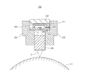
図2は、光書込み装置113主要な構成を示す断面図である。図2に示されるように、光書込み装置113は、OLEDパネル200とロッドレンズアレイ(SLA: Selfoc Lens Array)220をホルダー230に収容したものであって、OLEDパネル200上には多数のOLED201が主走査方向に沿ってライン状に実装されている。
[2] Configuration of
FIG. 2 is a cross-sectional view showing the main configuration of the
OLED201はそれぞれ光ビームLを出射し、ロッドレンズアレイ220は感光体ドラム111の外周面上に光ビームLを集光する。OLED201が封止カバー202によって覆われる一方、封止カバー202の外部には薄膜配線203が形成されており、外部電源から給電を受けて各OLED201に電流を供給する経路の一部となっている。
OLEDパネル200には導電性接着剤211によって線膨張調整部材210が接着されている。線膨張調整部材210は導電性を有する板金部材であって、その材料としては、ステンレス鋼(SUS 410: Steel Use Stainless 410)やアルミニウム(Al)を用いることができる。また、導電性接着剤211は導電性粒子を含んだ接着剤で、少なくとも固着後に導電性を有する。
Each
A linear
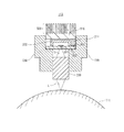
図3は、OLEDパネル200の概略平面図であり、併せてA−A´線における断面図とC−C´線における断面図も示されている。図2に示されたOLEDパネル200の断面は、D−D´線における断面である。また、概略平面図部分は後述する封止板を取り外した状態を示しており、封止カバー202がE−E´線における断面になっている。
図3に示されるように、OLEDパネル200は、TFT基板300、封止カバー202及びドライバーIC(Integrated Circuit)303等を備えている。TFT基板300は、ガラス基板301上にシリコン半導体材料を用いたTFT回路302を形成した後、OLED201を積層したものであって、多数のOLED201が主走査方向に沿ってライン状に配列されている。なお、ライン状に配列されたOLED201は、一列になっていても良いし、千鳥配置になっていても良い。
FIG. 3 is a schematic plan view of the
As shown in FIG. 3, the
また、TFT基板300のOLED201が配設された基板面は封止領域となっており、封止カバー202が封着されている。これによって、封止領域が、外気に触れないように乾燥窒素等を封入した状態で、封止される。なお、吸湿のため、封止領域内に吸湿剤を併せて封入しても良い。なお、封止カバー202は、例えば、封止ガラスであっても良いし、ガラス以外の材料からなっていても良い。
Further, the substrate surface on which the
TFT基板300の封止領域外にはドライバーIC303が実装されている。制御部102の輝度信号出力部310はフレキシブルワイヤー311を介してドライバーIC303にデジタル輝度信号を入力する。ドライバーIC303はデジタル輝度信号をアナログ輝度信号に変換してOLED201毎の駆動回路に入力する。駆動回路は輝度信号に応じてOLED201の駆動電流を生成する。なお、本実施の形態において、アナログ輝度信号は電圧信号である。
A
TFT回路302のうち、各OLED201に電流を供給する電源配線の一部203は、TFT基板300の封止領域外に形成されている。図4は、TFT回路302の概略構成を示す図である。図4に示されるように、TFT回路302は、給電点(図示省略)において定電圧Vcを供給する定圧電源400に電気的に接続された電源配線401であって、各OLED201に電流を供給するための電源配線401を備えている。
In the
駆動回路430は、電源配線401と各接続点402において接続されており、DAC401が出力するアナログ輝度信号に応じて、OLED201に供給する駆動電流量を制御する。駆動回路430からOLED201に供給された駆動電流は、最終的に接地端子420へ流される。
m番目の駆動回路430は接続点電位Vc(m)と、DAC(Digital to Analogue Converter)410が出力するアナログ輝度信号との電位差Vg(m)に応じた駆動電流をm番目のOLED201に供給する。OLED201は、駆動電流量に応じた発光量で発光する。DAC410は、ドライバーIC内に実装されており、輝度信号出力部310が出力したデジタル輝度信号をアナログ輝度信号に変換して各駆動回路430に順次、アナログ輝度信号を出力する。
The
The
電源配線401は、給電点(若しくは、定圧電源400)から各接続点402に向かう回路上において、電源配線203と電気的に並列接続されている。図2、3に示されるように、導電性の線膨張調整部材210は、導電性接着剤211によって電源配線203に電気的に並列接続されている。
このようにすれば、給電点から各接続点402に向かう回路のインピーダンスを低減させることができるので、電源配線401に電流が流れることによって発生する各接続点電位Vc(m)の電圧降下を抑制することができる。
The
In this way, since the impedance of the circuit from the feeding point to each
[3]温度変化に起因する画質劣化を防止するための構成
次に、温度変化に起因する画質劣化を防止するための構成について説明する。
本実施の形態に係る線膨張調整部材210は、封止カバー202やTFT基板300よりも線膨張係数が大きくなっており、温度変化によって、封止カバー202やTFT基板300よりも大きく膨張、収縮する。
[3] Configuration for Preventing Image Quality Degradation Caused by Temperature Change Next, a configuration for preventing image quality degradation caused by temperature change will be described.
The linear
また、図2に示されるように、線膨張調整部材210は、薄層の導電性接着剤211によって封止カバー202の上面全体に接着されている。封止カバー202は非導電性の接着剤によってTFT基板300に広範囲に亘って接着されている。また、線膨張調整部材210と封止カバー202、並びに封止カバー202とTFT基板300は、何れも十分な接着強度で接着されている。
Further, as shown in FIG. 2, the linear
このため、線膨張調整部材210が温度変化によって、膨張、収縮すると、封止カバー202が伸張、圧縮されるので、TFT基板300もまた伸張されたり圧縮されたりする。従って、温度変化に起因するTFT基板300の膨張、収縮が促進されるので、ロッドレンズアレイ220との線膨張差が小さくなる。すると、TFT基板300とロッドレンズアレイ220との線膨張差に起因するOLED201の出射光のスポット形状の変形が抑制されるので、当該スポット形状の変形に起因する画質の劣化が防止される。
For this reason, when the linear
例えば、TFT基板300のガラス基板部分の線膨張係数が約5ppm/℃であり、ロッドレンズアレイ220の線膨張係数は約19ppm/℃であるような場合を考えると、温度が1℃上昇する毎に、基準点から100mmの位置において、TFT基板300は0.5μm伸張するのに対して、ロッドレンズアレイ220は1.9μm伸張する。このため、線膨張差は1.4μmとなる。
For example, considering the case where the linear expansion coefficient of the glass substrate portion of the
解像度が1200dpiの光書込み装置ではOLED201のピッチが1.2μmであるため、1.4μmの線膨張差が発生するとOLED201の出射光のビーム形状が変形してしまい実用に耐えない。
これに対して、本実施の形態によれば、線膨張係数が約11ppm/℃であるステンレス鋼や、約23ppm/℃であるアルミニウムからなる線膨張調整部材210を用いてTFT基板300を伸張、圧縮させれば、温度変化に起因する線膨張差を小さくすることができるので、ビーム形状の変形を抑制して、画質向上を図ることができる。
In the optical writing device having a resolution of 1200 dpi, the pitch of the
In contrast, according to the present embodiment, the
[4]変形例
以上、本発明を実施の形態に基づいて説明してきたが、本発明が上述の実施の形態に限定されないのは勿論であり、以下のような変形例を実施することができる。なお、以下の変形例においては、上記実施の形態において対応する部材がある部材に上記実施の形態と同じ符号が付されている。
[4] Modifications As described above, the present invention has been described based on the embodiments. However, the present invention is not limited to the above-described embodiments, and the following modifications can be implemented. . In the following modifications, the same reference numerals as those in the above embodiment are given to members having corresponding members in the above embodiment.
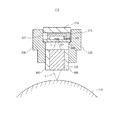
(1)TFT基板300やロッドレンズアレイ220は、環境温度の変化の他に、OLED201の発熱によっても温度変化する。このため、OLED201からロッドレンズアレイ220に伝導する熱量を低減することができれば、ロッドレンズアレイ220の熱膨張を抑えて、ロッドレンズアレイ220とTFT基板との線膨張差に起因する画質の劣化を防止することができる。
(1) The temperature of the
図5は、本変形例に係る光書込み装置113の主要な構成を示す断面図である。図5に示されるように、本変形例に係る光書込み装置113は、線膨張調整部材210に放熱フィン500が形成されていることを特徴とする。このようにすれば、OLED201を含むTFT基板300が発生させる熱が原因となって、ロッドレンズアレイ220とTFT基板300との間に線膨張差が生じるのを抑制して、画質の劣化を防止することができる。
FIG. 5 is a cross-sectional view showing the main configuration of the
また、放熱フィン500は、線膨張調整部材210の長手方向に沿って延設されている。このようにすれば、線膨張調整部材210とTFT基板300との線膨張差に起因して、線膨張調整部材210がその長手方向に沿ってTFT基板300側へ反るのを防止することができるので、TFT基板300の湾曲によってOLED201の出射光のスポット形状が変形して、画質が劣化するのを防止することができる。
Further, the
(2)TFT基板300とロッドレンズアレイ220との線膨張差を小さくするためには、TFT基板300を伸張、圧縮するのみならず、これに併せてロッドレンズアレイ220も圧縮、伸張するのが効果的である。
図6は、本変形例に係る光書込み装置113の主要な構成を示す断面図である。図6に示されるように、本変形例に係る光書込み装置113は、TFT基板300を伸張、圧縮する線膨張調整部材210に加えて、ロッドレンズアレイ220を圧縮、伸張する線膨張調整部材600を備えていることを特徴とする。線膨張調整部材600は、ロッドレンズアレイ220の長手方向であって、且つ光軸に平行な側面の全面に亘って接着、固定されている。
(2) In order to reduce the linear expansion difference between the
FIG. 6 is a cross-sectional view showing the main configuration of the
なお、線膨張調整部材600の線膨張係数は、線膨張調整部材210の線膨張係数と同一であって、且つ、TFT基板300の線膨張係数とロッドレンズアレイ220の線膨張係数との中間とするのが望ましい。このようにすれば、TFT基板300のみを伸張、圧縮させる場合と比較して、TFT基板300の伸張量、圧縮量を少なくすることができる。
The linear expansion coefficient of the linear
従って、伸張、圧縮によってTFT基板300に加わる機械的な負荷を低減することができると共に、TFT基板300を伸張、圧縮させる線膨張調整部材210に加わる機械的な負荷を低減することができる。従って、線膨張調整部材210として剛性のより低い材料を採用することが可能になる。更に、線膨張調整部材210、600に同じ材料を用いることができるという意味において、材料コストを低減することができる。
Therefore, the mechanical load applied to the
また、線膨張調整部材600よりも線膨張調整部材210の方が、線膨張係数が大きくても、TFT基板300とロッドレンズアレイ220との線膨張差をある程度、低減する効果を得ることができるのは言うまでも無い。逆に、線膨張調整部材600よりも線膨張調整部材210の方が、線膨張係数が小さい場合には、TFT基板300とロッドレンズアレイ220との線膨張差を更に小さくする効果がある。
Further, even if the linear
線膨張調整部材210、600にどのような線膨張係数を有する材料を用いるかについては、TFT基板300とロッドレンズアレイ220との線膨張差の許容範囲と、これらの部材に要求される伸張、圧縮に対する耐久性と、の兼ね合いによって決定すべきである。
(3)上記変形例においては、TFT基板300とロッドレンズアレイ220とで個別に線膨張調整部材210、600を設ける場合について説明したが、本発明がこれに限定されないのは言うまでも無く、次のようにしても良い。すなわち、上記変形例における線膨張調整部材210、600を一体化すれば、部品点数が削減されるので、光書込み装置113の部品コストを低減することができる。
Regarding the material having the linear expansion coefficient used for the linear
(3) In the above modification, the case where the linear
図7は、本変形例に係る光書込み装置113の主要な構成を示す断面図である。図7に示されるように、本変形例に係る光書込み装置113は、対向して配置された1対の線膨張調整部材700を備えている。線膨張調整部材700は、何れも長手方向に直交する断面形状がクランク状になっており、段部700aを有している。TFT基板300はロッドレンズアレイ220側の主面が、短手方向の両縁部において段部700aに接着、固定される。
FIG. 7 is a cross-sectional view showing the main configuration of the
線膨張調整部材700は、TFT基板300とロッドレンズアレイ220との何れに対しても、ロッドレンズアレイ220の長手方向であって、且つ光軸に平行な側面の全面に亘って接着、固定されている。これによって、ロッドレンズアレイ220は1対の線膨張調整部材700に挟持されることになる。
本変形例においては、線膨張係数の大小関係が
ロッドレンズアレイ220 > 線膨張調整部材700 > TFT基板300
となっており、温度変化に起因するロッドレンズアレイ220やTFT基板300の膨張、収縮が線膨張調整部材700によって規制される。従って、ロッドレンズアレイ220とTFT基板300との線膨張差に起因する画質の劣化を防止することができる。
The linear
In this modification, the magnitude relationship between the linear expansion coefficients is as follows:
Thus, the expansion and contraction of the
また、TFT基板300のTFT回路302が形成された主面上においては、当該主面の短手方向における両縁部に薄膜配線203が形成されており、給電点から各OLED201までの電流供給経路になっている。薄膜配線203は何れも導電性接着剤211によって1対の線膨張調整部材700のそれぞれに電気的に並列接続されている。本実施の形態において、1対の線膨張調整部材700は何れも導電性を有しているので、給電点から各OLED201までの電流供給経路のインピーダンスを更に低下させることができる。
Further, on the main surface of the
従って、電源配線における電圧低下に起因するOLED201の光量ムラを低減することができるので、画質の向上を図ることができる。
なお、1対の線膨張調整部材700の外側面は、全面に亘ってホルダー230に覆われている。ホルダー230は絶縁性の材料からなっており、導電性の線膨張調整部材700と感光体ドラム111との間における放電を防止する。従って、感光体度ドラム111の外周面上に形成される静電潜像に及ぼす放電の悪影響を防止して、高画質を実現することができる。
Therefore, the unevenness in the amount of light of the
The outer surfaces of the pair of linear
また、光書込み装置113のメンテナンス時において、保守作業員が線膨張調整部材700に直接触れて感電事故が発生するのも防止することができる。なお、ホルダー230に代えて、線膨張調整部材700の外側面に絶縁膜を形成しても良い。
(4)上記実施の形態においては、タンデム型のカラープリンター装置を例にとって説明したが、本発明がこれに限定されないのは言うまでも無く、タンデム型以外の方式のカラープリンター装置やモノクロプリンター装置に本発明を適用しても良い。
In addition, during maintenance of the
(4) In the above embodiment, the tandem type color printer apparatus has been described as an example. However, it goes without saying that the present invention is not limited to this, and a color printer apparatus or monochrome printer apparatus of a system other than the tandem type. The present invention may be applied to.
また、スキャナー装置を備えたコピー装置や、更にファクシミリ通信機能を備えたファクシミリ装置、或いはこれらの機能を兼ね備えた複合機(MFP: Multi-Function Peripheral)に本発明を適用しても同様の効果を得ることができる。 The same effect can be obtained by applying the present invention to a copying machine equipped with a scanner, a facsimile machine equipped with a facsimile communication function, or a multi-function peripheral (MFP) having these functions. Can be obtained.
本発明に係る光書込み装置及び画像形成装置に関し、特に、複数の原因によって低下し得る書き込み精度を低コストで向上させることができる装置として有用である。 The optical writing apparatus and the image forming apparatus according to the present invention are particularly useful as an apparatus that can improve writing accuracy that can be lowered due to a plurality of causes at low cost.
1……………………………画像形成装置
113、1000…………光書込み装置
201………………………OLED
202………………………封止カバー
203………………………薄膜配線
210、600、700…線膨張調整部材
211………………………導電性接着剤
220………………………ロッドレンズアレイ
300………………………TFT基板
401………………………電源配線
402………………………接続点
500………………………放熱フィン
1 ………………………………
202... ......
Claims (14)
前記ガラス基板上にライン状に配列された複数の電流駆動型発光素子と、
前記発光素子に沿って延設された薄膜配線であって、給電点から各発光素子への電流供給経路となる電源線と、
前記発光素子の出射光を集光するロッドレンズアレイと、
導電性を有すると共に、前記ガラス基板よりも線膨張係数が大きい線膨張調整部材と、を備え、
前記線膨張調整部材は、
前記ガラス基板に対して直接又は間接的に固定されており、且つ、前記給電点から各発光素子への電流供給経路となるように、前記電源線に電気的に並列接続されている
ことを特徴とする光書込み装置。 A glass substrate;
A plurality of current-driven light emitting elements arranged in a line on the glass substrate;
A thin-film wiring extending along the light-emitting element, a power line serving as a current supply path from a feeding point to each light-emitting element;
A rod lens array for condensing the light emitted from the light emitting element;
A linear expansion adjusting member having electrical conductivity and having a larger linear expansion coefficient than the glass substrate,
The linear expansion adjusting member is
It is fixed directly or indirectly to the glass substrate, and is electrically connected in parallel to the power supply line so as to be a current supply path from the feeding point to each light emitting element. Optical writing device.
前記線膨張調整部材は、前記封止部材に固定されることによって、前記ガラス基板に間接的に固定されている
ことを特徴とする請求項1に記載の光書込み装置。 A sealing member for sealing the light emitting element, which is sealed to a main surface of the glass substrate on which the light emitting element is mounted;
The optical writing device according to claim 1, wherein the linear expansion adjusting member is indirectly fixed to the glass substrate by being fixed to the sealing member.
ことを特徴とする請求項2に記載の光書込み装置。 The glass substrate and the sealing member, and the linear expansion adjusting member and the sealing member are bonded with a strength that can maintain the bonding state regardless of the linear expansion difference between the glass substrate and the rod lens array. The optical writing device according to claim 2, wherein:
ことを特徴とする請求項1から3の何れかに記載の光書込み装置。 4. The optical writing device according to claim 1, wherein the power supply line and the linear expansion adjusting member are electrically connected by a conductive adhesive.
ことを特徴とする請求項1から4の何れかに記載の光書込み装置。 The optical writing device according to claim 1, wherein the linear expansion adjusting member is a sheet metal member.
ことを特徴とする請求項5に記載の光書込み装置。 6. The optical writing device according to claim 5, wherein the linear expansion adjusting member has a rigidity that does not warp due to a difference in linear expansion from the glass substrate.
ことを特徴とする請求項5又は6に記載の光書込み装置 7. The optical writing device according to claim 5, wherein the linear expansion adjusting member is made of either stainless steel or aluminum.
ことを特徴とする請求項1から6の何れかに記載の光書込み装置。 The optical writing device according to claim 1, wherein the linear expansion adjusting member has a heat radiating rib formed on a side opposite to the glass substrate.
ことを特徴とする請求項8に記載の光書込み装置。 The optical writing device according to claim 8, wherein the heat radiating rib extends along a longitudinal direction of the linear expansion adjusting member.
前記ガラス基板、前記線膨張調整部材、前記ロッドレンズアレイの順に線膨張係数が大きくなる
ことを特徴とする請求項1に記載の光書込み装置。 The linear expansion adjusting member is further fixed to a side surface parallel to both the light emitting direction and the arrangement direction of the light emitting elements among the side surfaces of the rod lens array.
The optical writing device according to claim 1, wherein a linear expansion coefficient increases in the order of the glass substrate, the linear expansion adjusting member, and the rod lens array.
ことを特徴とする請求項10に記載の光書込み装置。 The optical writing device according to claim 10, wherein the linear expansion adjusting member is integrally formed.
ことを特徴とする請求項11に記載の光書込み装置。 The optical writing device according to claim 11, wherein an outer surface of the linear expansion adjusting member is covered with an insulating member.
ことを特徴とする請求項1から12の何れかに記載の光書込み装置。 The optical writing device according to claim 1, wherein the light emitting element is an OLED.
ことを特徴とする画像形成装置。 An image forming apparatus comprising the optical writing device according to claim 1.
Priority Applications (1)
| Application Number | Priority Date | Filing Date | Title |
|---|---|---|---|
| JP2014135824A JP6365019B2 (en) | 2014-07-01 | 2014-07-01 | Optical writing apparatus and image forming apparatus |
Applications Claiming Priority (1)
| Application Number | Priority Date | Filing Date | Title |
|---|---|---|---|
| JP2014135824A JP6365019B2 (en) | 2014-07-01 | 2014-07-01 | Optical writing apparatus and image forming apparatus |
Publications (2)
| Publication Number | Publication Date |
|---|---|
| JP2016013631A true JP2016013631A (en) | 2016-01-28 |
| JP6365019B2 JP6365019B2 (en) | 2018-08-01 |
Family
ID=55230245
Family Applications (1)
| Application Number | Title | Priority Date | Filing Date |
|---|---|---|---|
| JP2014135824A Active JP6365019B2 (en) | 2014-07-01 | 2014-07-01 | Optical writing apparatus and image forming apparatus |
Country Status (1)
| Country | Link |
|---|---|
| JP (1) | JP6365019B2 (en) |
Cited By (2)
| Publication number | Priority date | Publication date | Assignee | Title |
|---|---|---|---|---|
| JP2017170811A (en) * | 2016-03-24 | 2017-09-28 | コニカミノルタ株式会社 | Optical writing device and image formation apparatus |
| JP2018158484A (en) * | 2017-03-22 | 2018-10-11 | コニカミノルタ株式会社 | Optical writing apparatus and image forming apparatus |
Citations (4)
| Publication number | Priority date | Publication date | Assignee | Title |
|---|---|---|---|---|
| US4875057A (en) * | 1988-09-01 | 1989-10-17 | Eastman Kodak Company | Modular optical printhead for hard copy printers |
| JPH07147621A (en) * | 1993-11-22 | 1995-06-06 | Kyocera Corp | Image forming device |
| JP2010111102A (en) * | 2008-11-10 | 2010-05-20 | Seiko Epson Corp | Line head and image formaing apparatus |
| JP2014113747A (en) * | 2012-12-10 | 2014-06-26 | Konica Minolta Inc | Optical print head and image formation apparatus |
-
2014
- 2014-07-01 JP JP2014135824A patent/JP6365019B2/en active Active
Patent Citations (4)
| Publication number | Priority date | Publication date | Assignee | Title |
|---|---|---|---|---|
| US4875057A (en) * | 1988-09-01 | 1989-10-17 | Eastman Kodak Company | Modular optical printhead for hard copy printers |
| JPH07147621A (en) * | 1993-11-22 | 1995-06-06 | Kyocera Corp | Image forming device |
| JP2010111102A (en) * | 2008-11-10 | 2010-05-20 | Seiko Epson Corp | Line head and image formaing apparatus |
| JP2014113747A (en) * | 2012-12-10 | 2014-06-26 | Konica Minolta Inc | Optical print head and image formation apparatus |
Cited By (2)
| Publication number | Priority date | Publication date | Assignee | Title |
|---|---|---|---|---|
| JP2017170811A (en) * | 2016-03-24 | 2017-09-28 | コニカミノルタ株式会社 | Optical writing device and image formation apparatus |
| JP2018158484A (en) * | 2017-03-22 | 2018-10-11 | コニカミノルタ株式会社 | Optical writing apparatus and image forming apparatus |
Also Published As
| Publication number | Publication date |
|---|---|
| JP6365019B2 (en) | 2018-08-01 |
Similar Documents
| Publication | Publication Date | Title |
|---|---|---|
| US7541619B2 (en) | Electro-optical device, image forming apparatus, and image reader | |
| JP6123702B2 (en) | Optical writing apparatus and image forming apparatus | |
| CN110361947B (en) | Optical writing device and image forming apparatus | |
| US10031437B2 (en) | Light emitting device and image forming device | |
| JP6288038B2 (en) | Light emitting device, optical writing device, and image forming apparatus | |
| JP6825416B2 (en) | Optical writing device and image forming device equipped with it | |
| JP6365019B2 (en) | Optical writing apparatus and image forming apparatus | |
| JP2007261064A (en) | Image forming apparatus | |
| US20170168413A1 (en) | Optical writing device and image forming device | |
| KR101425490B1 (en) | Exposure head and producing method thereof, cartridge, and image forming apparatus | |
| JP4840304B2 (en) | Light emitting device and image forming apparatus having the same | |
| US20110242260A1 (en) | Optical head and image forming apparatus | |
| US20190064733A1 (en) | Optical scanning device and image forming device having the same | |
| JP2009099379A (en) | Light-emitting device and electronic equipment | |
| JP2007290330A (en) | Image forming apparatus | |
| JP6569502B2 (en) | Organic EL module, optical writing device, and image forming apparatus | |
| JP6750442B2 (en) | Optical writing device and image forming apparatus | |
| US20220197177A1 (en) | Exposure head and image forming apparatus | |
| JP6950487B2 (en) | Optical writing device and image forming device | |
| US10663919B2 (en) | Image forming apparatus including optical print head | |
| JP6699459B2 (en) | Optical writing device and image forming apparatus | |
| US9594327B2 (en) | Optical writing device and image forming apparatus | |
| JP2014217986A (en) | Light-emitting device, optical writing device, and image forming device | |
| JP2016099582A (en) | Light emitting device and image forming apparatus | |
| JP6264061B2 (en) | Optical writing apparatus and image forming apparatus |
Legal Events
| Date | Code | Title | Description |
|---|---|---|---|
| A621 | Written request for application examination |
Free format text: JAPANESE INTERMEDIATE CODE: A621 Effective date: 20170419 |
|
| A977 | Report on retrieval |
Free format text: JAPANESE INTERMEDIATE CODE: A971007 Effective date: 20180214 |
|
| A131 | Notification of reasons for refusal |
Free format text: JAPANESE INTERMEDIATE CODE: A131 Effective date: 20180220 |
|
| A521 | Request for written amendment filed |
Free format text: JAPANESE INTERMEDIATE CODE: A523 Effective date: 20180329 |
|
| TRDD | Decision of grant or rejection written | ||
| A01 | Written decision to grant a patent or to grant a registration (utility model) |
Free format text: JAPANESE INTERMEDIATE CODE: A01 Effective date: 20180605 |
|
| A61 | First payment of annual fees (during grant procedure) |
Free format text: JAPANESE INTERMEDIATE CODE: A61 Effective date: 20180618 |
|
| R150 | Certificate of patent or registration of utility model |
Ref document number: 6365019 Country of ref document: JP Free format text: JAPANESE INTERMEDIATE CODE: R150 |