JP2016005161A - Imaging device and driving method thereof - Google Patents
Imaging device and driving method thereof Download PDFInfo
- Publication number
- JP2016005161A JP2016005161A JP2014125047A JP2014125047A JP2016005161A JP 2016005161 A JP2016005161 A JP 2016005161A JP 2014125047 A JP2014125047 A JP 2014125047A JP 2014125047 A JP2014125047 A JP 2014125047A JP 2016005161 A JP2016005161 A JP 2016005161A
- Authority
- JP
- Japan
- Prior art keywords
- amplifier
- signal
- current
- pixel
- switch
- Prior art date
- Legal status (The legal status is an assumption and is not a legal conclusion. Google has not performed a legal analysis and makes no representation as to the accuracy of the status listed.)
- Pending
Links
Images


Abstract
Description
本発明は、撮像装置及びその駆動方法に関する。 The present invention relates to an imaging apparatus and a driving method thereof.
特許文献1には、行列状に画素が設けられた画素アレイの各列から信号を読み出すための読み出し回路が記載されている。特許文献1に記載の読み出し回路は、画素アレイの各行に接続された増幅回路と、増幅回路の後段に接続された保持容量とを有している。この読み出し回路では、画素アレイから信号を読み出す際、増幅回路から出力された信号を保持容量に保持させる期間以外は増幅回路を非動作状態とすることにより、消費電力の低減が図られている。
しかしながら、低消費電力化はバッテリー駆動の長時間化や動作に伴う発熱の抑制等の様々なメリットがあるため、さらに消費電力の低い撮像装置やその駆動方法が求められている。 However, since low power consumption has various merits such as longer battery driving and suppression of heat generation due to operation, an imaging device with lower power consumption and its driving method are required.
本発明の目的は、より消費電力の低い撮像装置及びその駆動方法を提供することにある。 An object of the present invention is to provide an imaging apparatus with lower power consumption and a driving method thereof.
本発明の一観点によれば、光電変換により生成された信号電荷を電圧信号として出力する画素と、前記画素からの出力信号が入力される増幅器、前記増幅器に電流を供給する電流源及び前記増幅器の入力端子と出力端子との間の導通と非導通とを切り替えるスイッチを有する増幅回路を含む読み出し回路とを有する撮像装置の駆動方法であって、前記スイッチを導通状態とし、前記増幅器の前記入力端子及び前記出力端子の電位をリセットするステップと、前記スイッチを非導通状態とし、前記画素からの前記出力信号を増幅するステップとを有し、前記増幅器の前記入力端子及び前記出力端子の電位をリセットするステップにおいて前記増幅器に供給する前記電流の平均値が、前記出力信号を増幅するステップにおいて前記増幅器に供給する前記電流の平均値よりも小さくなるように、前記電流源を制御することを特徴とする撮像装置の駆動方法が提供される。 According to one aspect of the present invention, a pixel that outputs a signal charge generated by photoelectric conversion as a voltage signal, an amplifier that receives an output signal from the pixel, a current source that supplies current to the amplifier, and the amplifier And a readout circuit including an amplifier circuit having a switch that switches between conduction and non-conduction between an input terminal and an output terminal of the imaging device, wherein the switch is turned on, and the input of the amplifier Resetting the potential of the terminal and the output terminal; and setting the switch to a non-conductive state and amplifying the output signal from the pixel, the potentials of the input terminal and the output terminal of the amplifier being The average value of the current supplied to the amplifier in the resetting step is supplied to the amplifier in the step of amplifying the output signal. As less than the mean value of the current, the driving method of the imaging device and controls the current source is provided.
本発明の他の一観点によれば、光電変換素子により生成された信号電荷を電圧信号として出力する画素と、前記画素からの出力信号が入力される増幅器、前記増幅器に電流を供給する電流源及び前記増幅器の入力端子と出力端子との間の導通と非導通とを切り替えるスイッチを有する増幅回路を含む読み出し回路と、前記スイッチを導通状態として前記増幅器の前記入力端子及び前記出力端子の電位をリセットする際に前記増幅器へ供給する前記電流の平均値が、前記スイッチを非導通状態として前記画素から読み出した信号を増幅する際に前記増幅器へ供給する前記電流の平均値よりも小さくなるように、前記電流源を制御する制御手段とを有することを特徴とする撮像装置が提供される。 According to another aspect of the present invention, a pixel that outputs a signal charge generated by a photoelectric conversion element as a voltage signal, an amplifier that receives an output signal from the pixel, and a current source that supplies current to the amplifier And a readout circuit including an amplifier circuit having a switch that switches between conduction and non-conduction between the input terminal and the output terminal of the amplifier, and the potentials of the input terminal and the output terminal of the amplifier are set to the conduction state, The average value of the current supplied to the amplifier when resetting is smaller than the average value of the current supplied to the amplifier when a signal read from the pixel is amplified with the switch turned off. There is provided an imaging device comprising a control means for controlling the current source.
また、本発明の更に他の一観点によれば、画素信号及びリセット信号を電圧信号として出力する画素と、前記画素から前記画素信号が入力される第1の増幅器と、前記第1の増幅器に電流を供給する第1の電流源と、前記第1の増幅器の前記入力端子と前記第1の増幅器の出力端子との間の導通と非導通とを切り替える第1のスイッチとを有する第1の増幅回路と、前記画素から前記リセット信号が入力される第2の増幅器と、前記第2の増幅器に電流を供給する第2の電流源と、前記第2の増幅器の前記入力端子と前記第2の増幅器の出力端子との間の導通と非導通とを切り替える第2のスイッチとを有する第2の増幅回路と、前記第1のスイッチを導通状態として前記第1の増幅器の前記入力端子及び前記出力端子の電位をリセットする際に前記第1の増幅器へ供給する前記電流の平均値が前記第1のスイッチを非導通状態として前記画素信号を増幅する際に前記第1の増幅器へ供給する前記電流の平均値よりも小さくなるように前記第1の電流源を制御し、前記第2のスイッチを導通状態として前記第2の増幅器の前記入力端子及び前記出力端子の電位をリセットする際に前記第2の増幅器へ供給する前記電流の平均値が前記第2のスイッチを非導通状態として前記リセット信号を増幅する際に前記第2の増幅器へ供給する前記電流の平均値よりも小さくなるように前記第2の電流源を制御する制御手段とを有することを特徴とする撮像装置が提供される。 According to still another aspect of the present invention, a pixel that outputs a pixel signal and a reset signal as a voltage signal, a first amplifier that receives the pixel signal from the pixel, and the first amplifier A first current source that supplies current; and a first switch that switches between conduction and non-conduction between the input terminal of the first amplifier and the output terminal of the first amplifier. An amplifier circuit; a second amplifier to which the reset signal is input from the pixel; a second current source for supplying a current to the second amplifier; the input terminal of the second amplifier; A second amplifier circuit having a second switch for switching between conduction and non-conduction with the output terminal of the amplifier, and the input terminal of the first amplifier and the first switch with the first switch in a conduction state Reset the output terminal potential The average value of the current supplied to the first amplifier is smaller than the average value of the current supplied to the first amplifier when the pixel signal is amplified with the first switch in a non-conductive state. Controlling the first current source to supply the second amplifier when the second switch is turned on to reset the potential of the input terminal and the output terminal of the second amplifier. The second current source is controlled so that the average value of the current is smaller than the average value of the current supplied to the second amplifier when the reset signal is amplified when the second switch is turned off. There is provided an image pickup apparatus having a control means.
また、本発明の更に他の一観点によれば、増幅器と、前記増幅器に電流を供給する電流源と、一方の端子に信号が与えられ、他方の端子が前記増幅器の入力端子に接続された容量と、前記増幅器の前記入力端子と前記増幅器の出力端子との間の導通と非導通とを切り替えるスイッチと、前記スイッチが導通状態のときに前記増幅器に供給する前記電流の平均値が、前記スイッチが非導通状態のときに前記増幅器に供給する前記電流の平均値よりも小さくなるように、前記電流源を制御する制御手段とを有することを特徴とする増幅回路が提供される。 According to still another aspect of the present invention, an amplifier, a current source that supplies current to the amplifier, a signal is given to one terminal, and the other terminal is connected to an input terminal of the amplifier. Capacitance, a switch that switches between conduction and non-conduction between the input terminal of the amplifier and the output terminal of the amplifier, and an average value of the current supplied to the amplifier when the switch is in a conduction state, There is provided an amplifying circuit comprising control means for controlling the current source so as to be smaller than an average value of the current supplied to the amplifier when the switch is in a non-conducting state.
本発明によれば、撮像装置の消費電力を低減することができる。 According to the present invention, the power consumption of the imaging apparatus can be reduced.
[第1実施形態]
本発明の第1実施形態による増幅回路及びその駆動方法について図1乃至図3を用いて説明する。
[First Embodiment]
An amplifier circuit and a driving method thereof according to a first embodiment of the present invention will be described with reference to FIGS.
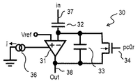
図1は、本実施形態による増幅回路の構成を示す回路図である。図2は、本実施形態による増幅回路に用いられる増幅器の一例を示す回路図である。図3は本実施形態による増幅回路の駆動方法を示すタイミング図である。 FIG. 1 is a circuit diagram showing the configuration of the amplifier circuit according to the present embodiment. FIG. 2 is a circuit diagram showing an example of an amplifier used in the amplifier circuit according to the present embodiment. FIG. 3 is a timing diagram illustrating a method of driving the amplifier circuit according to the present embodiment.
はじめに、本実施形態による増幅回路の構成について図1及び図2を用いて説明する。 First, the configuration of the amplifier circuit according to the present embodiment will be described with reference to FIGS.
本実施形態による増幅回路30は、図1に示すように、増幅器31と、クランプ容量32と、帰還容量33と、スイッチ34と、定電流源36とを有している。クランプ容量32の一方の端子は増幅回路30の入力端子37を構成し、クランプ容量32の他方の端子は増幅器31の反転入力端子に接続されている。増幅器31の非反転入力端子には、基準電圧である電圧Vrefが入力されている。増幅回路30の出力端子38を構成する増幅器31の出力端子と、増幅器31の反転入力端子との間には、帰還容量33とスイッチ34とが並列に接続されている。スイッチ34は、例えばN型MOSトランジスタであり、主ノードであるソース及びドレインの一方が増幅器31の反転入力端子に接続され、ソース及びドレインの他方が増幅器31の出力端子に接続されている。
As shown in FIG. 1, the
スイッチ34の導通状態は、スイッチ34の制御ノード(N型MOSトランジスタのゲート)に印加される信号(クランプパルス信号pc0r)によって制御される。ここでは、クランプパルス信号pc0rがHighレベル(以下、「Hレベル」と表記する)のとき、スイッチ34が導通状態(オン状態)になるものとする。また、クランプパルス信号pc0rがLowレベル(以下、「Lレベル」と表記する)のとき、スイッチ34が非導通状態(オフ状態)になるものとする。
The conduction state of the
増幅器31は、例えば図2に示す回路により構成される。図2に示す増幅器31は、1段の差動増幅回路であり、P型MOSトランジスタ40,41と、N型MOSトランジスタ42,43とを有している。P型MOSトランジスタ40,41のソースは、電源電圧線に接続されている。P型MOSトランジスタ40,41のゲートは、P型MOSトランジスタ41のドレイン及びN型MOSトランジスタ43のドレインに接続されている。P型MOSトランジスタ40のドレインは、N型MOSトランジスタ42のドレインに接続されている。N型MOSトランジスタ42,43のソースは、電流源36を構成するN型MOSトランジスタ44のドレインに接続されている。N型MOSトランジスタ44のソースは、接地電圧線に接続されている。
The
図2の増幅器31では、N型MOSトランジスタ42のゲートが増幅器31の反転入力端子(図中、「in−」)を構成し、N型MOSトランジスタ43のゲートが増幅器31の非反転入力端子(図中、「in+」)を構成する。また、P型MOSトランジスタ40のドレインとN型MOSトランジスタ42のドレインとの接続ノードが、増幅器31の出力端子38(図中、「out」)を構成する。N型MOSトランジスタ44のゲートは、電流源36の電流制御用のバイアス端子であり、このゲートに印加される信号VB_tailによって電流源36を流れる電流Iが制御される。
In the
なお、クランプパルス信号pc0r及び信号VB_tailは、後述する駆動方法に従い、図示しない制御手段により適宜制御される。 The clamp pulse signal pc0r and the signal VB_tail are appropriately controlled by a control unit (not shown) according to a driving method described later.
次に、本実施形態による増幅回路の駆動方法について図1乃至図3を用いて説明する。 Next, the driving method of the amplifier circuit according to the present embodiment will be explained with reference to FIGS.
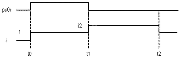
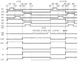
本実施形態による増幅回路の駆動方法は、増幅器31のオフセットレベルをクランプ容量32にクランプするためのクランプ動作と、入力信号を増幅する増幅動作とを含む。図3のタイミング図において、時刻t0〜時刻t1がクランプ動作の期間に相当し、時刻t1〜時刻t2が増幅動作の期間に相当する。
The driving method of the amplifier circuit according to the present embodiment includes a clamp operation for clamping the offset level of the
まず、増幅動作に先立ち、増幅器31のクランプ動作を行う。すなわち、時刻t0において、クランプパルス信号pc0rをHレベルとし、スイッチ34を導通状態にする。また、同じく時刻t0において、信号VB_tailのレベルを、電流源36の電流Iが電流i1となるように制御して、増幅器31を動作させる(以下、「第1の動作モード」と呼ぶ)。これにより、増幅器31は電圧フォロワ状態となり、出力端子の電圧は電圧Vrefにほぼ等しくなる。そして、増幅器31の反転入力端子の電位は、電圧Vrefに対して増幅器31のオフセット電圧を加えたオフセットレベルとなり、クランプ容量32にクランプされる。こうして、増幅器31の入力端子及び出力端子の電位をリセットする。
First, the
次いで、入力信号の増幅動作を行う。すなわち、時刻t1において、クランプパルス信号pc0rをLレベルとし、スイッチ34を非導通状態にする。また、信号VB_tailのレベルを、N型MOSトランジスタ44の電流Iが電流i2となるように制御して、増幅器31を動作させる(以下、「第2の動作モード」と呼ぶ)。これにより、増幅器31が増幅可能な状態となり、入力端子37からクランプ容量32を介して入力された電圧信号が増幅されて出力端子38から出力される。
Next, an input signal amplification operation is performed. That is, at time t1, the clamp pulse signal pc0r is set to L level, and the
次いで、増幅信号を他の回路へ出力した後、時刻t2において、信号VB_tailを所定のレベルに設定し、N型MOSトランジスタ44に流れる電流量を減らすことにより、増幅器31による消費電力を低減する。図3においては、時刻t2に、電流Iを電流i1とした例を示しているが、電流Iの供給を停止しても良い。
Next, after the amplified signal is output to another circuit, at time t2, the signal VB_tail is set to a predetermined level, and the amount of current flowing through the N-
ここで、本実施形態による増幅回路の駆動方法では、第1の動作モード時に電流源36により供給する電流i1を、第2の動作モード時に電流源36により供給する電流i2よりも小さい値に設定する。第1の動作モード時における電流源36の電流i1は、第2の動作モード時における電流源36の電流i2よりも小さければ特に限定されるものではないが、例えば、第2の動作モード時における電流源36の電流i2の半分程度とすることができる。
Here, in the driving method of the amplifier circuit according to the present embodiment, the current i1 supplied from the
これにより、クランプ動作から増幅動作までの一連の動作の際に電流源36の電流Iを増幅動作時の電流(本実施形態の電流i2に相当)と同じにする場合と比較して、消費電流を低減することができる。例えば、電流i1を電流i2の半分程度(i1=i2/2)とした本発明者等による試作検討結果では、消費電力を約1/2に抑制できることが確認された。
As a result, compared to the case where the current I of the
第2の動作モード時では、信号増幅精度を維持する観点から、電流源36により供給する電流i2を減少して消費電流の低減を図るには限界がある。本実施形態のように、第2の動作モード時における電流i2はそのままに、第1の動作モード時における電流i1を低減することにより、信号増幅精度の維持と消費電流の低減との双方を実現することができる。
In the second operation mode, there is a limit in reducing the current consumption by reducing the current i2 supplied from the
なお、第1の動作モード時の電流i1を小さくしすぎると、トータルの消費電流は大幅に抑制できる反面、増幅器31のオフセット電圧の除去が不十分になる。逆に、第2の動作モード時の電流i2に対して僅かしか電流i1を減少しなければ、消費電流の低減効果を十分に得ることはできない。第1の動作モード時の電流i1を第2の動作モード時の電流i2と比較してどの程度減少させるかについては、消費電力の低減効果に加えて、増幅回路30に求められる特性等をも考慮して適宜決定することが望ましい。本発明者等による試作検討結果では、第1の動作モード時の電流i1を、第2の動作モード時の電流i2のおよそ10%〜25%程度に低減しても、増幅器31のオフセット除去量が実用上問題のないレベルに収まることが確認された。
Note that if the current i1 in the first operation mode is too small, the total current consumption can be significantly suppressed, but the offset voltage of the
図3のタイミング図では、時刻t1において、クランプパルス信号pc0rのHレベルからLレベル遷移と、増幅器31の電流Iの電流i1から電流i2への切り替えとを、同じタイミングで行っているが、これらは必ずしも同じタイミングで行う必要はない。例えば、クランプ解除にあたるクランプパルス信号pc0rのLレベルへの遷移よりも少し前に、電流i1から電流i2へ切り替えるようにしてもよい。クランプ解除前に短時間でも増幅時と同じ定電流値に変化しておくことにより、増幅器31のオフセットレベルへのクランプ動作をより確実に行うことができる。これにより、時刻t0〜時刻t1の間において供給電流を低減したことに伴い生じうるクランプエラーを抑制することができる。
In the timing chart of FIG. 3, at time t1, the transition from the H level to the L level of the clamp pulse signal pc0r and the switching of the current I of the
少なくともクランプ動作時に増幅器31に供給される電流の平均値が増幅動作時に増幅器31に供給される電流の平均値よりも小さくなるように電流源の制御を行うことで、消費電流低減の効果は得ることができる。増幅器31の電流Iを電流i1から電流i2へ切り替えるタイミングは、所望の消費電流低減効果が得られる範囲内で適宜変更が可能である。
By controlling the current source so that at least the average value of the current supplied to the
なお、本実施形態の増幅回路30では、反転入力端子と出力端子の間に帰還容量33を接続しているが、他の容量で保持した信号を増幅する抵抗型など、他の構成の増幅器であってもよい。
In the
このように、本実施形態によれば、クランプ動作時に増幅器に供給する電流を、増幅動作時に増幅器に供給する電流よりも少なくしてトータルの消費電流を低減するので、増幅回路の消費電力を低減することができる。 As described above, according to the present embodiment, the current supplied to the amplifier during the clamp operation is less than the current supplied to the amplifier during the amplification operation to reduce the total current consumption, thereby reducing the power consumption of the amplifier circuit. can do.
[第2実施形態]
本発明の第2実施形態による撮像装置及びその駆動方法について図4乃至図8を用いて説明する。図1乃至図3に示す第1実施形態による増幅回路と同様の構成要素には同一の符号を付し説明を省略し或いは簡潔にする。
[Second Embodiment]
An image pickup apparatus and a driving method thereof according to the second embodiment of the present invention will be described with reference to FIGS. The same components as those of the amplifier circuit according to the first embodiment shown in FIGS. 1 to 3 are denoted by the same reference numerals, and description thereof is omitted or simplified.
図4は、本実施形態による撮像装置の構成を示す概略図である。図5は、本実施形態による撮像装置の画素の構成の一例を示す回路図である。図6は、本実施形態による撮像装置の信号読み出し回路の構成の一例を示す回路図である。図7は、本実施形態による撮像装置の増幅回路の増幅器の構成の一例を示す回路図である。図8は、本実施形態による撮像装置の駆動方法を示すタイミング図である。 FIG. 4 is a schematic diagram illustrating the configuration of the imaging apparatus according to the present embodiment. FIG. 5 is a circuit diagram illustrating an example of a pixel configuration of the imaging apparatus according to the present embodiment. FIG. 6 is a circuit diagram illustrating an example of the configuration of the signal readout circuit of the imaging apparatus according to the present embodiment. FIG. 7 is a circuit diagram showing an example of the configuration of the amplifier of the amplifier circuit of the imaging apparatus according to the present embodiment. FIG. 8 is a timing diagram illustrating the driving method of the imaging apparatus according to the present embodiment.
はじめに、本実施形態による撮像装置の構成について図4乃至図7を用いて説明する。 First, the configuration of the imaging apparatus according to the present embodiment will be described with reference to FIGS. 4 to 7.
本実施形態による撮像装置100は、図4に示すように、画素アレイ10、垂直走査回路11、タイミングジェネレータ(以下、「TG」と表記する)12、読み出し回路70、水平転送回路13、水平走査回路14、出力アンプ15を有している。
As illustrated in FIG. 4, the
画素アレイ10は、行方向及び列方向に沿って2次元マトリクス状に配列された複数の画素20を有している。図4には図面の簡略化のために4行4列の画素アレイ10を示しているが、行方向及び列方向に配置される画素20の数は特に限定されるものではない。なお、本明細書において、行方向とは図面において横方向を示し、列方向とは図面において縦方向を示すものとする。一例では、行方向が撮像装置における水平方向に対応し、列方向が撮像装置における垂直方向に対応する。
The
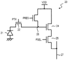
画素20は、例えば図5に示すように、光電変換素子であるフォトダイオード21、転送MOSトランジスタ22、リセットMOSトランジスタ23、増幅MOSトランジスタ24、選択MOSトランジスタ25を、それぞれ有している。
For example, as illustrated in FIG. 5, the
フォトダイオード21のアノードは接地電圧線に接続され、カソードは転送MOSトランジスタ22のソースに接続されている。転送MOSトランジスタ22のドレインは、リセットMOSトランジスタ23のソース及び増幅MOSトランジスタ24のゲートに接続されている。転送MOSトランジスタ22のドレイン、リセットMOSトランジスタ23のソース及び増幅MOSトランジスタ24のゲートの接続ノードは、フローティングディフュージョン領域(以下、「FD領域」という)26を構成する。リセットMOSトランジスタ23及び増幅MOSトランジスタ24のドレインは、電源電圧線(VDD)に接続されている。増幅MOSトランジスタ24のソースは、選択MOSトランジスタ25のドレインに接続されている。転送MOSトランジスタ22、リセットMOSトランジスタ23、増幅MOSトランジスタ24、選択MOSトランジスタ25は、フォトダイオード21から画素信号を読み出すための画素内読み出し回路を構成する。
The anode of the
なお、トランジスタのソース及びドレインの呼称は、トランジスタの導電型や着目する機能等に応じて異なることがあり、上述のソースとドレインとは逆の名称で呼ばれることもある。また、本明細書では、MOSトランジスタをスイッチと呼ぶこともある。この場合、ソース及びドレインを主ノード、ゲートを制御ノードと呼ぶものとする。 Note that the names of the source and the drain of the transistor may differ depending on the conductivity type of the transistor, the function of interest, and the like, and the above-described source and drain may be referred to as opposite names. In this specification, the MOS transistor is sometimes called a switch. In this case, the source and drain are called the main node, and the gate is called the control node.
画素アレイ10の各行には、行方向に延在して、信号線TX、信号線RES、信号線SEL(いずれも図示せず)が、それぞれ配置されている。信号線TXは、行方向に並ぶ画素20の転送MOSトランジスタ22のゲートにそれぞれ接続され、これら画素20に共通の信号線をなしている。信号線RESは、行方向に並ぶ画素20のリセットMOSトランジスタ23のゲートにそれぞれ接続され、これら画素20に共通の信号線をなしている。信号線SELは、行方向に並ぶ画素20の選択MOSトランジスタ25のゲートにそれぞれ接続され、これら画素20に共通の信号線をなしている。なお、図4では、図面の簡略化のために、信号線TX、信号線RES、信号線SELをまとめて1本の信号線readとして表している。また、信号線readの名称には、行番号に対応した番号をそれぞれ付記している(read1,read2,read3,read4)。
In each row of the
垂直走査回路11は、TG12からのタイミング信号に基づいて画素20を行ごとに選択して、当該行に属する各画素20から画素信号を出力させるための制御を行うものである。信号線read(信号線TX、信号線RES、信号線SEL)は、垂直走査回路11に接続されている。信号線TXには、垂直走査回路11から、転送MOSトランジスタ22を駆動するための転送パルス信号PTXが出力される。信号線RESには、垂直走査回路11から、リセットMOSトランジスタ23を駆動するためのリセットパルス信号PRESが出力される。信号線SELには、垂直走査回路11から、選択MOSトランジスタ25を駆動するための選択パルス信号PSELが出力される。これら信号線にHレベルの信号が印加されると、対応するトランジスタが導通状態(オン状態)となる。また、Lレベルの信号が印加されると、対応するトランジスタが非導通状態(オフ状態)となる。
The
画素アレイ10の各列には、列方向に延在して、垂直信号線27がそれぞれ配置されている。垂直信号線27は、列方向に並ぶ画素20のそれぞれの選択MOSトランジスタ25のソースに接続され、これら画素20に共通の信号線をなしている。各列の垂直信号線27には、増幅MOSトランジスタ24の負荷手段としての定電流源28と、読み出し回路70とが接続されている。
In each column of the
読み出し回路70は、図4に示すように、増幅回路30と、ラインメモリ60とを有している。増幅回路30及びラインメモリ60は、例えば図6に示す回路により構成することができる。
As shown in FIG. 4, the
図6に示す増幅回路30は、図1の増幅回路30において、帰還容量33を、選択的に接続可能な複数の帰還容量33a,33b,33c,33d,33eに変更したものである。すなわち、増幅器31の反転入力端子と出力端子との間には、帰還容量33aとスイッチ35aとの直列接続体が、スイッチ34と並列に接続されている。同様に、帰還容量33bとスイッチ35bとの直列接続体、帰還容量33cとスイッチ35cとの直列接続体、帰還容量33dとスイッチ35dとの直列接続体及び帰還容量33eとスイッチ35eとの直列接続体が、スイッチ34と並列に接続されている。
The
帰還容量33a,33b,33c,33d,33eは、互いに異なる容量値を有している。例えば、帰還容量33a,33b,33c,33d,33eの容量値は、クランプ容量32の容量値をC0として、それぞれ、C0,C0/2,C0/4,C0/8,C0/16に設定されている。
The
スイッチ35a,35b,35c,35d,35eの導通状態は、スイッチ34の制御ノードに印加される信号(制御パルス信号PGCa,PGCb,PGCc,PGCd,PGCe)によって制御される。制御パルス信号PGCがHレベルのとき、対応するスイッチ35がオン状態となり、対応する帰還容量33が増幅器31の反転入力端子と出力端子との間に接続される。制御パルス信号PGCによる感度切り替えによって帰還容量33のいずれか1つを選択することにより、増幅回路30による電圧増幅率を、1倍、2倍、4倍、8倍、16倍に切り替えることができる。
The conduction states of the
このように、本実施形態の増幅回路30は、被写体の明るさに応じて増幅回路30のゲインを切り替えることを可能とし、撮像装置として広ダイナミックレンジを実現したものである。
As described above, the
増幅回路30による電圧増幅率が上がることで、出力アンプ15で発生するノイズの影響を相対的に軽減し、被写体が暗いときのS/N比の悪化を抑制することが可能である。その一方で、増幅段の電圧増幅率が上がるにつれて、増幅器31に対して高い開ループゲインが要求される。
By increasing the voltage amplification factor by the
そこで、本実施形態の増幅回路30においては、増幅器31を、図7に示すようなカスコード型の高利得増幅回路としている。
Therefore, in the
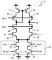
図7に示す増幅器31は、P型MOSトランジスタ40,41,45,46と、N型MOSトランジスタ42,43,47,48,49,50,51,52とを有している。電源電圧線と接地電圧線との間に、P型MOSトランジスタ40,45、N型MOSトランジスタ47,42,49,51が、この順で直列に接続されている。同様に、電源電圧線と接地電圧線との間に、P型MOSトランジスタ41,46、N型MOSトランジスタ48,43,50,52が、この順で直列に接続されている。P型MOSトランジスタ40,41のゲートは、P型MOSトランジスタ46のドレインとN型MOSトランジスタ48のソースとの接続ノードに接続されている。N型MOSトランジスタ42のソースとN型MOSトランジスタ49のドレインとの接続ノードは、N型MOSトランジスタ43のソースとN型MOSトランジスタ50のドレインとの接続ノードに接続されている。
The
図7に示す増幅器31では、N型MOSトランジスタ42のゲートが増幅器31の反転入力端子(図中、「in−」)を構成し、N型MOSトランジスタ43のゲートが増幅器31の非反転入力端子(図中、「in+」)を構成する。また、P型MOSトランジスタ45のドレインとN型MOSトランジスタ47のドレインとの接続ノードが、増幅器31の出力端子38(図中、「out」)を構成する。
In the
信号VB_Hは、ゲート接地P型MOSトランジスタ45,46へのバイアス電圧である。信号VB_Lは、ゲート接地NMOSトランジスタ47,48へのバイアス電圧である。図7に示す増幅器31は、テレスコピック・カスコード型となっているが、例えば電源電圧が低い場合は、フォールデッド・カスコード型の増幅回路を用いてもよい。
The signal VB_H is a bias voltage to the common-gate P-
N型MOSトランジスタ51,52は、図2のN型MOSトランジスタ44に対応する定電流源として機能するものである。本実施形態の増幅器31は、これらN型MOSトランジスタ51,52により構成される2つの定電流源を有しているともいえる。これらN型MOSトランジスタ51,52は、ゲートに印加される信号VB_tailの信号レベルにより、流れる電流i1,i2を制御することができる。或いは、N型MOSトランジスタ51,52のサイズ(ゲート幅)を変えておき、一定の信号レベルの信号VB_tailによって、N型MOSトランジスタ52には電流i1が流れ、NMOSトランジスタ51には電流i2が流れるようにしてもよい。なお、N型MOSトランジスタ51,52の電流量の制御方法は、特に限定されるものではなく、これらの組み合わせや他の方法を用いてもよい。
The N-
N型MOSトランジスタ49,50は、N型MOSトランジスタ51,52により構成される2つの定電流源の導通/非導通を制御するためのスイッチである。N型MOSトランジスタ49は、このゲートに印加される信号Icon2により、導通/非導通が制御される。N型MOSトランジスタ50は、このゲートに印加される信号Icon1により、導通/非導通が制御される。
The N-
N型MOSトランジスタ49,50は、ゲートに印加される信号Hレベルのときオン状態となり、Lレベルのときオフ状態となる。すなわち、信号Icon1がHレベルで信号Icon2がLレベルのとき、増幅器31には電流i1が流れて動作状態となる。信号Icon1がLレベルで信号Icon2がHレベルのとき、増幅器31には電流i2が流れて動作状態となる。信号Icon1,Icon2がともにHレベルのとき、増幅器31には電流i1+i2が流れて動作状態となる。信号Icon1,Icon2がともにLレベルのとき、増幅器31に電流は流れず非動作状態となる。
The N-
本実施形態の撮像装置を、例えばデジタルカメラの撮像系に適用する場合、デジタルカメラのISO感度調整手段として、図6の増幅回路を利用することが好適である。なお、本実施形態では、ゲインの切り替えを帰還容量の切り替えによって行っているが、クランプ容量の切り替えによって行ってもよく、また、両者を併用してもよい。 When the imaging apparatus of the present embodiment is applied to, for example, an imaging system of a digital camera, it is preferable to use the amplifier circuit of FIG. 6 as the ISO sensitivity adjustment unit of the digital camera. In this embodiment, the gain is switched by switching the feedback capacitor. However, the gain may be switched by switching the clamp capacitor, or both may be used in combination.
ラインメモリ60は、図6に示すように、スイッチ61N,61S,63N,63Sと、容量62N,62Sとを有している。スイッチ61N,61Sの一方の主ノードは、増幅回路30の出力端子38に接続されている。スイッチ61Nの他方の主ノードは、スイッチ63Nの一方の主ノード及び容量62Nの一方の端子に接続されている。スイッチ61Sの他方の主ノードは、スイッチ63Sの一方の主ノード及び容量62Sの一方の端子に接続されている。スイッチ63N,63Sの他方の端子は、水平転送回路13に接続されている。容量62N,62Sの他方の端子は、固定電圧線(例えば接地電圧線)に接続されている。容量62N,62Sは、画素20から読み出され増幅回路30により増幅されたリセット信号及び画素信号を、水平転送回路13により転送する前に一時的に保持するための信号保持容量である。
As shown in FIG. 6, the
読み出し回路70は、水平転送回路13に接続されている。水平転送回路13は、水平走査回路14及び出力アンプ15に接続されている。水平走査回路14は、TG12に接続されている。
The
次に、本実施形態による撮像装置の駆動方法について図4乃至図9を用いて説明する。なお、以下の説明では、1つの画素20の読み出し動作について主に説明するが、同じ行に属する異なる列の複数の画素20についてのラインメモリ60までの信号読み出し動作は、並行して同時に行われる。
Next, the driving method of the imaging apparatus according to the present embodiment will be described with reference to FIGS. In the following description, the read operation of one
まず、時刻t0において、リセットパルス信号PRESをHレベルとし、リセットMOSトランジスタ23をオン状態とする。これにより、FD領域26がリセットMOSトランジスタ30を介して電源電圧線に電気的に接続され、FD領域26がリセットレベルの電位(リセット電位)にリセットされる。
First, at time t0, the reset pulse signal PRES is set to H level, and the reset MOS transistor 23 is turned on. As a result, the
また、同じく時刻t0において、信号Icon1をHレベルとし、クランプ動作時用の定電流回路のスイッチであるN型MOSトランジスタ50をオン状態とする。このとき、信号VB_tailに所定の電圧を印加しておき、N型MOSトランジスタ52にクランプ動作時用の電流i1が流れるようにしておく。また、信号Icon2はLレベルとし、増幅動作時用の定電流回路のスイッチであるN型MOSトランジスタ49は、オフ状態のままとする(i2=0)。これにより、増幅器31には、N型MOSトランジスタ50,52を介して電流i1が流れ、増幅器31が動作状態(第1の動作モード)となる。このときの増幅器31への供給電流Iは、I=i1である。
Similarly, at time t0, the signal Icon1 is set to the H level, and the N-
また、同じく時刻t0において、クランプパルス信号pc0rをHレベルとし、スイッチ34をオン状態とする。これにより、増幅器31は電圧フォロワ状態となり、出力端子の電圧は電圧Vrefにほぼ等しくなる。そして、増幅器31の反転入力端子の電位は、電圧Vrefに対して増幅器31のオフセット電圧を加えたオフセットレベルとなる。こうして、増幅器31の入力端子及び出力端子の電位をリセットする。
Similarly, at time t0, the clamp pulse signal pc0r is set to the H level, and the
次いで、FD領域26のリセットが完了後、時刻t1において、リセットパルス信号PRESをLレベルとし、FD領域26を信号読み出し可能なようにフローティング状態とする。
Next, after the reset of the
次いで、時刻t2において、選択パルス信号PSELをHレベルとし、選択MOSトランジスタ25をオンとする。これにより、増幅MOSトランジスタ24は、ソースに垂直信号線27及び選択MOSトランジスタ25を介して定電流源28からバイアス電流が供給された状態となり、ソースフォロワ回路を構成する。そしてこれによって、垂直信号線27には、増幅MOSトランジスタ24の入力ノードの電位、すなわちリセット電位であるFD領域26の電位に基づく信号(リセット信号)が、選択MOSトランジスタ25を介して出力される。
Next, at time t2, the selection pulse signal PSEL is set to H level, and the
これにより、増幅回路30の入力端子37がリセット信号の電位となり、増幅器31の反転入力端子がオフセットレベルの電位となり、この電位関係が基準としてクランプ容量32にクランプされる。
As a result, the
次いで、増幅器31のクランプ動作が完了後、時刻t3において、クランプパルス信号pc0rをLレベルとし、スイッチ34をオフ状態とする。これにより、増幅器31の反転入力端子と出力端子とが帰還容量33を介して接続され、増幅器31が増幅可能な状態となる。
Next, after the clamp operation of the
また、同じく時刻t3において、また、信号Icon2をHレベルとし、増幅動作時用の定電流回路のスイッチであるN型MOSトランジスタ49をオン状態とする。このとき、信号VB_tailに所定の電圧を印加しておき、N型MOSトランジスタ49に増幅動作時用の定電流i2が流れるようにしておく。また、信号Icon1はLレベルに切り替え、クランプ動作時用の定電流回路のスイッチであるN型MOSトランジスタ50はオフ状態にする(i1=0)。これにより、増幅器31には、N型MOSトランジスタ49,51を介して電流i2が流れ、増幅器31が動作状態(第2の動作モード)となる。このときの増幅器31への供給電流Iは、I=i2である。
Similarly, at time t3, the signal Icon2 is set to the H level, and the N-
垂直信号線27に出力された画素20からのリセット信号は、クランプ容量32を介して増幅器31の反転入力端子に入力されている。これにより、増幅器31は、クランプ容量32を介して垂直信号線27から与えられたリセット信号を増幅し、出力端子38から出力する。このとき、増幅器31の帰還経路には帰還容量33が接続されているため、クランプ容量32と帰還容量33との比によってゲインが決定される。
The reset signal from the
次いで、時刻t4において、信号PTNをHレベルとしてスイッチ61Nをオン状態とし、増幅回路30の出力端子38をラインメモリ60の容量62Nに接続する。これにより、増幅回路30により増幅されたリセット信号を、容量62Nに書き込む。
Next, at time t4, the signal PTN is set to H level to turn on the
次いで、容量62Nへのリセット信号の書き込み完了後、時刻t5において、信号PTNをLレベルとしてスイッチ61Nをオフ状態とする。これにより、リセット信号は、容量62Nにより保持された状態となる。
Next, after completing the writing of the reset signal to the
次いで、時刻t6において、転送パルス信号PTXをHレベルとし、転送MOSトランジスタ22をオン状態とする。これにより、フォトダイオード21において光電変換により生成された信号電荷が、FD領域26に転送される。そして、垂直信号線27には、フォトダイオード21から転送された信号電荷の量に応じたFD領域26の電位に基づく信号(画素信号)が、選択MOSトランジスタ25を介して出力される。
Next, at time t6, the transfer pulse signal PTX is set to H level, and the transfer MOS transistor 22 is turned on. Thereby, the signal charge generated by the photoelectric conversion in the
次いで、FD領域26への信号電荷の転送完了後、時刻t7において、転送パルス信号PTXをLレベルとし、転送MOSトランジスタ22をオフ状態とする。
Next, after the transfer of the signal charge to the
垂直信号線27に出力された画素信号は、クランプ容量32を介して増幅器31の反転入力端子に入力されている。これにより、増幅器31は、クランプ容量32を介して垂直信号線27から与えられた画素信号を増幅し、出力端子38から出力する。このとき、増幅器31の帰還経路には帰還容量33が接続されているため、クランプ容量32と帰還容量33との比によってゲインが決定される。
The pixel signal output to the
次いで、時刻t8において、信号PTSをHレベルとしてスイッチ61Sをオン状態とし、増幅回路30の出力端子38をラインメモリ60の容量62Sに接続する。これにより、増幅回路30により増幅された画素信号を、容量62Sに書き込む。
Next, at time t8, the signal PTS is set to H level to turn on the switch 61S, and the
次いで、容量62Sへの画素信号の書き込み完了後、時刻t9において、信号PTSをLレベルとしてスイッチ61Sをオフ状態とする。これにより、画素信号は、容量62Sにより保持された状態となる。 Next, after completing the writing of the pixel signal to the capacitor 62S, at time t9, the signal PTS is set to L level to turn off the switch 61S. As a result, the pixel signal is held by the capacitor 62S.
次いで、時刻t10において、信号Icon2をLレベルにして増幅動作時の定電流回路をオフにして、増幅器31をパワーダウンする。
Next, at time t10, the signal Icon2 is set to L level, the constant current circuit during the amplification operation is turned off, and the
次いで、水平走査回路14により水平転送回路13を制御し、容量62Nに蓄積された画素リセット信号と、容量62Sに蓄積された画素信号とを、水平転送回路13へ列ごとに順次読み出す。そして、水平転送回路13へ読み出された出力信号を、順次出力アンプ15或いはチップ外のICへ転送し、相関二重サンプリング処理等の信号処理を行い、画像信号を取得する。
Next, the
上述の本実施形態による撮像装置の駆動方法において、時刻t0〜時刻t3において増幅器31に供給する電流i1及び時刻t3〜時刻t10において増幅器31に供給する電流i2の設定方法は、第1実施形態の場合と同様である。増幅器31の電流i1,i2をこのように設定することで、信号増幅精度を維持しつつ、消費電流を低減することができる。
In the driving method of the image pickup apparatus according to the present embodiment described above, the setting method of the current i1 supplied to the
なお、図8のタイミング図では、時刻t3において、クランプパルス信号pc0r、信号Icon1、信号Icon2を同時に遷移しているが、これら信号は必ずしも同時に遷移する必要はない。例えば、クランプ解除にあたるクランプパルス信号pc0rのLレベルへの遷移よりも少し前に、信号Icon1及び信号Icon2を遷移するようにしてもよい。クランプ解除前に短時間でも増幅時と同じ定電流値に変化させておくことにより、増幅器31のオフセットレベルへのクランプ動作をより確実に行うことができる。これにより、時刻t0〜時刻t3の間において供給電流を低減したことに伴い生じうるクランプエラーを抑制することができる。
In the timing chart of FIG. 8, the clamp pulse signal pc0r, the signal Icon1 and the signal Icon2 are simultaneously changed at the time t3, but these signals are not necessarily changed simultaneously. For example, the signal Icon1 and the signal Icon2 may be shifted slightly before the transition to the L level of the clamp pulse signal pc0r for releasing the clamp. By changing the constant current value to the same constant value as that at the time of amplification for a short time before releasing the clamp, the clamp operation to the offset level of the
少なくともクランプ動作時に増幅器31に供給される電流の平均値が増幅動作時に増幅器31に供給される電流の平均値よりも小さくなるように電流源の制御を行うことで、消費電流低減の効果は得ることができる。増幅器31の電流Iを電流i1から電流i2へ切り替えるタイミングは、所望の消費電流低減効果が得られる範囲内で適宜変更が可能である。
By controlling the current source so that at least the average value of the current supplied to the
本実施形態による撮像装置の駆動方法によれば、消費電力を大幅に低減することができる。増幅器31のクランプ時の供給電流を増幅時の供給電流よりも減らす場合、クランプ時と増幅時の供給電流を同じにする場合と比較すると、増幅器31のオフセットが除去しにくい方向ではある。しかしながら、多少オフセット量が増加しても使用できるアナログ回路は多く存在し、何より、オフセット量と消費電力のバランスの良いところを選択できるというフレキシビリティの高い増幅回路の駆動方法を実現することができる。
According to the driving method of the imaging apparatus according to the present embodiment, power consumption can be significantly reduced. When the supply current at the time of clamping of the
本実施形態では、増幅回路30に2つの定電流源を設け、クランプ動作時と増幅動作時とでこれら定電流源をスイッチにより切り替えることで、クランプ時における電流i1と増幅時における電流i2とを変化している。これは、1つの定電流源を用いて電流値を変化する場合よりも短時間で所望の定電流量を得られるからである。
In the present embodiment, two constant current sources are provided in the
定電流を1つの定電流源によって切り替えようとした場合、例えば図7の回路では、信号VB_tailの電圧値を変化させることになる。しかしながら、この方法では、所望の定電流量になるまでに、本実施形態の方法と比較して、より多くの時間を要する。これは、エリアセンサは通常のICとは異なり、列数に対応して例えば数千もの読み出し回路を有しており、各列に存在する信号VB_tailを変化する際に配線のCR時定数によって遅延が発生し、所望の電圧値に変化するまでに時間がかかるからである。電流値が定まらなければノイズの少ない正しい信号読み出しができないため、結果、撮像装置のフレームレートに影響を与えてしまう。 When switching the constant current by one constant current source, for example, in the circuit of FIG. 7, the voltage value of the signal VB_tail is changed. However, this method requires more time than the method of the present embodiment until a desired constant current amount is obtained. This is because, unlike a normal IC, an area sensor has, for example, thousands of readout circuits corresponding to the number of columns, and is delayed by the CR time constant of the wiring when the signal VB_tail existing in each column is changed. This is because it takes time to occur and change to a desired voltage value. If the current value is not determined, correct signal readout with less noise cannot be performed, and as a result, the frame rate of the imaging apparatus is affected.
また、信号VB_tailにより電流値を制御するMOSトランジスタのサイズは、増幅器31に必要な定電流量やダイナミックレンジの設計要件等に応じて決定される。これに対し、本実施形態における信号Icon1,Icon2で制御されるN型MOSトランジスタ49,50は、単なるスイッチであり、比較的自由にサイズを決めることが可能である。このスイッチを必要最低限のオン抵抗となるようなサイズとすれば、当該トランジスタのMOS容量を小さくすることができ、ひいては寄生容量を低減することができる。そして、信号VB_tailを常に所定の一定電圧を保ったままとすれば、結果として相対的に、2つの定電流源を用意して切り替える本実施形態の方式は、読み出し時間の増大を抑えるのに有効な手法となる。
The size of the MOS transistor that controls the current value by the signal VB_tail is determined according to the constant current amount necessary for the
また、本実施形態の撮像装置においては、設定ゲイン毎に消費電力低減モードを用いるか否かを適宜使い分けるのも有効である。 In the imaging apparatus of this embodiment, it is also effective to properly use whether or not to use the power consumption reduction mode for each set gain.
前述の通り、信号PGCa〜信号PGCeを制御することにより、増幅回路30のゲインを変更することが可能である。例えば、信号PGCa〜信号PGCeの総てをHレベルとしたときの増幅率を1倍とすると、信号PGCeのみをHレベルとし信号PGCa〜信号PGCdをLレベルとした場合には、最大で入力信号を16倍とするゲインをかけることが可能となる。しかしながら、このような高ゲイン設定時に実際に図8の駆動方法を行うと、増幅器31のオフセットレベル差が大きくなる。このためオフセットレベル差がオフセットクランプエラーとなって、撮像装置においては列ごとのオフセットばらつきとして見えてしまう可能性がある。
As described above, the gain of the
実際のカメラにおいては低ISO設定で撮影することの方が高ISO設定で撮影する頻度よりも多い。そのため、高ゲイン設定の読み出し時に消費電力低減よりも画質を優先する場合にはクランプ動作時に流す電流を増幅動作時と同じとする読み出しを行い、低ゲイン設定の読み出し時には本実施形態の駆動方法を用いて消費電力の低減を行ってもよい。 In an actual camera, shooting with a low ISO setting is more frequent than shooting with a high ISO setting. For this reason, when priority is given to image quality over power consumption reduction when reading high gain settings, reading is performed with the same current applied during clamp operation as during amplification operation, and the driving method of this embodiment is used when reading low gain settings. It may be used to reduce power consumption.
なお、本実施形態による撮像装置の駆動方法には、供給電流の低減に伴う効果として、消費電力の低減効果だけでなく、増幅器31の動作に伴う発熱や、ホットキャリアの発生及びその再結合による発光を低減する効果もある。そのため、本実施形態による撮像装置及びその駆動方法は、長時間蓄積を行う撮影が存在するカメラ用の光電変換装置に特に有用である。
Note that in the driving method of the imaging apparatus according to the present embodiment, not only the effect of reducing the power consumption, but also the heat generated by the operation of the
このように、本実施形態によれば、撮像装置の読み出し回路において、増幅器のクランプ動作時に供給する電流を増幅動作時に供給する電流よりも少なくしてトータルの消費電流を低減するので、撮像装置の読み出し動作時の消費電力を低減することができる。 As described above, according to the present embodiment, in the readout circuit of the imaging apparatus, the current supplied during the clamp operation of the amplifier is less than the current supplied during the amplification operation, thereby reducing the total current consumption. Power consumption during the read operation can be reduced.
[第3実施形態]
本発明の第3実施形態による撮像装置の駆動方法について図9を用いて説明する。図1乃至図3に示す第1実施形態による増幅回路及びその駆動方法並びに図4乃至図8に示す第2実施形態による撮像装置及びその駆動方法と同様の構成要素には同一の符号を付し説明を省略し或いは簡潔にする。
[Third Embodiment]
A driving method of the imaging apparatus according to the third embodiment of the present invention will be described with reference to FIG. Components similar to those of the amplifier circuit and the driving method thereof according to the first embodiment shown in FIGS. 1 to 3 and the imaging device and the driving method thereof according to the second embodiment shown in FIGS. 4 to 8 are denoted by the same reference numerals. The explanation is omitted or simplified.
図9は、本実施形態による撮像装置の駆動方法を示すタイミング図である。 FIG. 9 is a timing diagram illustrating the driving method of the imaging apparatus according to the present embodiment.
本実施形態では、図4乃至図7に示す第2実施形態による撮像装置の他の駆動方法について説明する。 In the present embodiment, another driving method of the imaging apparatus according to the second embodiment shown in FIGS. 4 to 7 will be described.
本実施形態による撮像装置の駆動方法では、図9に示すように、時刻t0から時刻t10までの間、信号Icon1をHレベルとして電流i1を流し、時刻t3から時刻t10までの間、信号Icon2をHレベルとして電流i2を流している。すなわち、クランプ動作時である時刻t0〜時刻t3における増幅器31への供給電流Iをi1とし、増幅モード時である時刻t3〜時刻t10における増幅器31への供給電流Iをi1+i2としている。
In the driving method of the image pickup apparatus according to the present embodiment, as shown in FIG. 9, the signal Icon1 is set to the H level from time t0 to time t10, the current i1 is supplied, and the signal Icon2 is applied from time t3 to time t10. The current i2 is supplied as the H level. That is, the supply current I to the
この場合、信号増幅精度の維持のために必要な増幅動作時の供給電流をIaとして、例えば、I1=I2=Ia/2に設定する。これにより、t0〜時刻t3における増幅器31への供給電流IはIa/2となり、時刻t3〜時刻t10における増幅器31への供給電流IはIaとなり、第2実施形態の場合と同じ供給電流となる。
In this case, for example, I 1 = I 2 = Ia / 2 is set as Ia, which is the supply current during the amplification operation necessary for maintaining the signal amplification accuracy. As a result, the supply current I to the
また、本実施形態による撮像装置の駆動方法では、N型MOSトランジスタ49に流す電流i2の値が小さくなるため、N型MOSトランジスタ49に求められる電流駆動能力、すなわちN型MOSトランジスタ49のサイズを小さくすることができる。これにより、増幅器31に必要な回路面積が小さくなり、チップサイズを縮小することができる。
Further, in the driving method of the image pickup apparatus according to the present embodiment, since the value of the current i2 flowing through the N-
なお、電流i1と電流i2とは必ずしも同じである必要はなく、電流I=i1+i2が信号増幅精度の維持のために必要な増幅動作時の供給電流Ia以上になる範囲で、適宜変更が可能である。 Note that the current i1 and the current i2 do not necessarily have to be the same, and can be appropriately changed as long as the current I = i1 + i2 becomes equal to or higher than the supply current Ia during the amplification operation necessary for maintaining the signal amplification accuracy. is there.
このように、本実施形態によれば、撮像装置の読み出し回路において、増幅器のクランプ動作時に供給する電流を増幅動作時に供給する電流よりも少なくしてトータルの消費電流を低減するので、撮像装置の読み出し動作時の消費電力を低減することができる。 As described above, according to the present embodiment, in the readout circuit of the imaging apparatus, the current supplied during the clamp operation of the amplifier is less than the current supplied during the amplification operation, thereby reducing the total current consumption. Power consumption during the read operation can be reduced.
[第4実施形態]
本発明の第4実施形態による撮像装置の駆動方法について図10及び図11を用いて説明する。図1乃至図3に示す第1実施形態による増幅回路及びその駆動方法並びに図4乃至図9に示す第2及び第3実施形態による撮像装置及びその駆動方法と同様の構成要素には同一の符号を付し説明を省略し或いは簡潔にする。
[Fourth Embodiment]
A driving method of the imaging apparatus according to the fourth embodiment of the present invention will be described with reference to FIGS. Components similar to those of the amplifier circuit and the driving method thereof according to the first embodiment shown in FIGS. 1 to 3 and the imaging device and the driving method thereof according to the second and third embodiments shown in FIGS. The description is omitted or simplified.
図10は、本実施形態による撮像装置の信号読み出し回路の構成の一例を示す回路図である。図11は、本実施形態による撮像装置の駆動方法を示すタイミング図である。 FIG. 10 is a circuit diagram illustrating an example of the configuration of the signal readout circuit of the imaging apparatus according to the present embodiment. FIG. 11 is a timing diagram illustrating the driving method of the imaging apparatus according to the present embodiment.
はじめに、本実施形態による撮像装置の構成について図10を用いて説明する。 First, the configuration of the imaging apparatus according to the present embodiment will be described with reference to FIG.
本実施形態による撮像装置100は、読み出し回路70の構成が異なるほかは、図4及び図5に示す第2実施形態による撮像装置と同様である。
The
本実施形態による撮像装置100の読み出し回路70は、図10に示すように、増幅器31を含む増幅回路30の後段に、増幅器64Sを含む増幅回路30Sと、増幅器64Nを含む増幅回路30Nと、の2系統の増幅回路を更に有している。
As shown in FIG. 10, the
増幅回路30は、図1に示す第1実施形態による増幅回路30と同様、増幅器31と、クランプ容量32と、帰還容量33と、スイッチ34とを有している。クランプ容量32の一方の端子は増幅回路30の入力端子37を構成し、クランプ容量32の他方の端子は増幅器31の反転入力端子に接続されている。増幅器31の非反転入力端子には、基準電圧である電圧Vrefが入力されている。増幅回路30の出力端子38を構成する増幅器31の出力端子と、増幅器31の反転入力端子との間には、帰還容量33とスイッチ34とが並列に接続されている。スイッチ34の導通状態は、スイッチ34の制御ノードに印加されるクランプパルス信号pc0rによって制御される。なお、本実施形態による撮像装置の増幅回路30として、図6及び図7に示す第2実施形態による撮像装置の増幅回路30を用いてもよい。
Similarly to the
増幅回路30Sは、増幅器64S、容量65S、スイッチ66S,67S,68S、電流源69Sを有している。増幅回路30Sの入力端子であるスイッチ66Sの一方の端子は、増幅回路30の出力端子38に接続されている。スイッチ66Sの他方の端子は、スイッチ68Sの一方の端子及び容量65Sの一方の端子に接続されている。容量65Sの他方の端子は、増幅器64Sの反転入力端子及びスイッチ67Sの一方の端子に接続されている。増幅器64Sの非反転入力端子には、基準電圧である電圧Vrefが入力されている。増幅回路30Sの出力端子を構成する増幅器64Sの出力端子には、スイッチ67Sの他方の端子及びスイッチ68Sの他方の端子が接続されている。増幅器64Sの出力端子は、ラインメモリ60のスイッチ61Sに接続されている。
The amplifier circuit 30S includes an amplifier 64S, a
スイッチ66S,67S,68S,61S,63Sは、それぞれ、制御信号SV1,SV2,SV3,SV4,SV5により制御される。これら信号がHレベルのとき、対応するスイッチが導通状態(オン状態)となる。また、これら信号がLレベルのとき、対応するスイッチが非導通状態(オフ状態)となる。 The switches 66S, 67S, 68S, 61S, 63S are controlled by control signals SV1, SV2, SV3, SV4, SV5, respectively. When these signals are at the H level, the corresponding switch is turned on (on state). Further, when these signals are at the L level, the corresponding switch is turned off (off state).
同様に、増幅回路30Nは、増幅器64N、容量65N、スイッチ66N,67N,68N、電流源69Nを有している。増幅回路30Nの入力端子であるスイッチ66Nの一方の端子は、増幅回路30の出力端子38に接続されている。スイッチ66Nの他方の端子は、スイッチ68Nの一方の端子及び容量65Nの一方の端子に接続されている。容量65Nの他方の端子は、増幅器64Nの反転入力端子及びスイッチ67Nの一方の端子に接続されている。増幅器64Nの非反転入力端子には、基準電圧である電圧Vrefが入力されている。増幅回路30Nの出力端子を構成する増幅器64Nの出力端子には、スイッチ67Nの他方の端子及びスイッチ68Nの他方の端子が接続されている。増幅器64Nの出力端子は、ラインメモリ60のアナログスイッチ61Nに接続されている。
Similarly, the
スイッチ66N,67N,68N,61N,63Nは、それぞれ、制御信号SR1,SR2,SR3,SR4,SR5により制御される。これら信号がHレベルのとき、対応するスイッチが導通状態(オン状態)となる。また、これら信号がLレベルのとき、対応するスイッチが非導通状態(オフ状態)となる。
増幅器64S,64Nは、例えば図2に示すような1段の差動増幅回路により構成され、この場合、電流源69S,69Nは、図2のN型MOSトランジスタ44に対応する。
The
次に、本実施形態による撮像装置の駆動方法について図11を用いて説明する。ここでは、画素アレイ10の第m行目、第n列目の画素20からの信号を読み出す場合の動作について、増幅回路30S,30Nの駆動方法を中心に説明する。画素20からの信号読み出し及び増幅回路30の駆動方法は、第2及び第3実施形態による撮像装置の駆動方法と同様であるため、適宜説明を省略する。
Next, the driving method of the imaging apparatus according to the present embodiment will be described with reference to FIG. Here, an operation in the case of reading a signal from the
まず、時刻t101において、信号Icon1をHレベルとし、増幅回路30S,30Nの定電流源69S,69Nに、クランプ動作時用の定電流i1をそれぞれ流す。なお、定電流源69Sから増幅器64Sへ供給される電流i1と、定電流源69Nから増幅回路64Nへ供給される電流i1とは、必ずしも同じである必要はない。
First, at time t101, the signal Icon1 is set to H level, and the constant current i1 for clamping operation is supplied to the constant current sources 69S and 69N of the
また、同じく時刻t101において、信号SV2及びSR2をHレベルとしてスイッチ67S,67Nをオン状態とし、容量65Sの他方の端子を増幅器64Sの出力端子に、また、容量65Nの他方の端子を増幅器64Nの出力端子に、それぞれ接続する。信号SV3,SR3,SV4,SR4はLレベルとし、スイッチ68S,68N,61S,61Nは、オフ状態としておく。
Similarly, at time t101, the signals SV2 and SR2 are set to the H level to turn on the
次いで、時刻t102において、信号SR1をHレベルとしてスイッチ66Nをオン状態とし、増幅回路30の出力端子38から出力されたリセット信号を、スイッチ66Nを介して容量65Nに書き込む。
Next, at time t102, the signal SR1 is set to H level to turn on the
次いで、時刻t103において、信号SR1をLレベルとしてスイッチ66Nをオフ状態とし、リセット信号を容量65Nにより保持する。この際、このリセット信号は、増幅器64Nのオフセットレベルに対してクランプされていることになる。
Next, at time t103, the signal SR1 is set to L level, the
ここで、時刻t102から時刻103において信号SR1をHレベルとするタイミングは、図8及び図9に示すタイミング図の時刻t4から時刻t5において信号PTNをHレベルとするタイミングに対応する。すなわち、時刻t102において、増幅回路30の出力端子38には、増幅されたリセット信号が出力されている。
Here, the timing at which the signal SR1 is set at the H level from the time t102 to the time 103 corresponds to the timing at which the signal PTN is set at the H level from the time t4 to the time t5 in the timing diagrams shown in FIGS. That is, at time t102, the amplified reset signal is output to the
次いで、時刻t104において、信号SV1をHレベルとしてスイッチ66Sをオン状態とし、増幅回路30の出力端子38から出力された画素信号を、スイッチ66Sを介して容量65Sに書き込む。
Next, at time t104, the signal SV1 is set to the H level, the switch 66S is turned on, and the pixel signal output from the
次いで、時刻t105において、信号SV1をLレベルとしてスイッチ66Sをオフ状態とし、画素信号を容量65Sにより保持する。この際、この画素信号は、増幅器64Sのオフセットレベルに対してクランプされていることになる。
Next, at time t105, the signal SV1 is set to L level, the switch 66S is turned off, and the pixel signal is held by the
ここで、時刻t104から時刻105において信号SV1をHレベルとするタイミングは、図8及び図9に示すタイミング図の時刻t8から時刻t9において信号PTSをHレベルとするタイミングに対応する。すなわち、時刻t104において、増幅回路30の出力端子38には、増幅された画素信号が出力されている。
Here, the timing at which the signal SV1 is at the H level from the time t104 to the time 105 corresponds to the timing at which the signal PTS is at the H level from the time t8 to the time t9 in the timing charts shown in FIGS. That is, at time t104, the amplified pixel signal is output to the
次いで、時刻t106において、信号SV2,SR2,Icon1をLレベルとし、代わりに信号Icon2をHレベルとし、増幅回路30S,30Nの定電流源69S,69Nに、増幅動作時用の定電流i2をそれぞれ流す。なお、定電流源69Sから増幅器64Sへ供給される電流i2と、定電流源69Nから増幅回路64Nへ供給される電流i2とは、必ずしも同じである必要はない。
Next, at time t106, the signals SV2, SR2, and Icon1 are set to L level, and the signal Icon2 is set to H level, and the constant current sources 69S and 69N of the
次いで、時刻t107において、信号SV3,SR3をHレベルとし、スイッチ68S,68Nをオン状態とする。これにより、増幅器64Sの反転入力端子と出力端子との間に容量65Sが、増幅器64Nの反転入力端子と出力端子との間に容量65Nが、それぞれ接続された状態となる。これにより、一定時刻の後、増幅器64Sの出力端子の電圧は、増幅器64Sの非反転入力端子の電圧Vrefとは無関係に、容量65Sに書き込まれた画素信号のレベルとなる。同様に、増幅器64Nの出力端子の電圧は、増幅器64Nの非反転入力端子の電圧Vrefとは無関係に、容量65Nに書き込まれた画素リセット信号のレベルとなる。
Next, at time t107, the signals SV3 and SR3 are set to the H level, and the
次いで、時刻t108において、信号SV4,SR4をHレベルとし、スイッチ61S,61Nをオン状態とする。これにより、増幅器64Sの出力端子と容量62Sとが接続され、容量62Sには画素信号が書き込まれる。また、増幅器64Nの出力端子と容量62Nとが接続され、容量62Nにはリセット信号が書き込まれる。
Next, at time t108, the signals SV4 and SR4 are set to the H level, and the
次いで、容量62S,62Nへの書き込みが終了した後、時刻t109において、信号SV4,SR4をLレベルとし、スイッチ61S,61Nをオフ状態とする。これにより、画素信号及びリセット信号は、それぞれ容量62S及び容量62Nに保持された状態となる。
Next, after the writing to the
次いで、時刻t110において、信号SV3,SR3をLレベルとしてスイッチ68S,68Nをオフ状態とする。
Next, at time t110, the signals SV3 and SR3 are set to L level, and the
このようにして時刻t110までの駆動を行うことにより、ラインメモリ60の各列の容量62Sにはm行目の画素からの画素信号がそれぞれ保持され、各列の容量62Nには第m行目の画素からのリセット信号がそれぞれ保持されたことになる。
By driving in this way until time t110, the pixel signal from the m-th row pixel is held in the capacitor 62S of each column of the
次いで、時刻t10以降、各列の信号SV5,SR5を順次Hレベルとしてスイッチ63S,63Nをオン状態とし、容量62Sに保持された画素信号と、容量62Nに保持されたリセット信号とを、水平転送回路13へ列ごとに順次読み出す。
Next, after time t10, the signals SV5 and SR5 of each column are sequentially set to H level to turn on the
その後、第(m+1)行の画素の読み出しのために、上述した第m行目の読み出し動作と同じ読み出し動作を、図11に示すように繰り返す(時刻t201〜時刻t210)。 Thereafter, in order to read out the pixels in the (m + 1) th row, the same read operation as the above-described read operation in the mth row is repeated as shown in FIG. 11 (time t201 to time t210).
このとき、信号Icon2は、図11に実線で示したように、第(m+1)行目の読み出し動作の開始時刻である時刻t201においてLレベルとしてもよいが、図11に点線で示したように時刻t110においてLレベルとしてもよい。すなわち、第m行目の読み出し動作の時刻t109においてスイッチ61S及び61Nをオフ状態とした時点で容量62S,62Nに信号は保持されるため、時刻109〜時刻t201の期間に増幅器64S,64Nに流れる定電流i2を停止しても問題ない。このようにすることで、増幅器64S,64Nの消費電流が更に低減され、更なる低消費電力化を図ることができる。
At this time, the signal Icon2 may be at the L level at time t201, which is the start time of the read operation of the (m + 1) th row as shown by the solid line in FIG. 11, but as shown by the dotted line in FIG. It may be at the L level at time t110. That is, since the signals are held in the
第m行目の画素20の画素信号及び画素リセット信号の水平転送回路13への読み出し動作は、第(m+1)行目の画素の読み出し動作において信号SV4,SR4をHレベルにするまで(時刻t208まで)のタイミングで行えばよい。容量62S,62Nからの読み出し前にスイッチ61S,61Nがオンになると、容量62S,62Nに蓄積されていた第m行目の信号が第(m+1)行目の信号によって上書きされてしまうからである。
The readout operation of the pixel signal and the pixel reset signal of the
換言すると、第(m+1)行目の画素についての時刻t201〜時刻t207までの動作は、図11に示すように、第m行目の画素の水平転送回路13への読み出し動作と並行して行うことができる。これにより、読み出し時間を短縮化することができる。
In other words, the operation from the time t201 to the time t207 for the pixel of the (m + 1) th row is performed in parallel with the reading operation of the pixel of the mth row to the
本実施形態の駆動方法において、時刻t101〜時刻t106において増幅器64S,64Nに流す電流i1及び時刻t6〜時刻t10において増幅器64S,64Nに流す電流i2の設定方法は、第1実施形態の場合と同様である。増幅器64S,64Nの電流i1,i2をこのように設定することで、信号増幅精度を維持しつつ、消費電流を低減することができる。
In the driving method of the present embodiment, the setting method of the current i1 that flows to the
このように、本実施形態によれば、撮像装置の読み出し回路において、増幅器のクランプ動作時に供給する電流を増幅動作時に供給する電流よりも少なくしてトータルの消費電流を低減するので、撮像装置の読み出し動作時の消費電力を低減することができる。 As described above, according to the present embodiment, in the readout circuit of the imaging apparatus, the current supplied during the clamp operation of the amplifier is less than the current supplied during the amplification operation, thereby reducing the total current consumption. Power consumption during the read operation can be reduced.
[第5実施形態]
本発明の第5実施形態による撮像システムについて図12を用いて説明する。図1乃至図3に示す第1実施形態による増幅回路及びその駆動方法並びに図4乃至図11に示す第2乃至第4実施形態による撮像装置及びその駆動方法と同様の構成要素には同一の符号を付し説明を省略し或いは簡潔にする。
[Fifth Embodiment]
An imaging system according to a fifth embodiment of the present invention will be described with reference to FIG. Components similar to those of the amplifier circuit and the driving method thereof according to the first embodiment shown in FIGS. 1 to 3 and the imaging device and the driving method thereof according to the second to fourth embodiments shown in FIGS. The description is omitted or simplified.
図12は、本実施形態による撮像システムの構成の一例を示す概略図である。 FIG. 12 is a schematic diagram illustrating an example of the configuration of the imaging system according to the present embodiment.
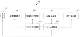
本実施形態による撮像システム800は、例えば、光学部810、撮像装置100、映像信号処理部830、記録・通信部840、タイミング制御部850、システム制御部860、及び再生・表示部870を含む。撮像装置100は、先の実施形態で説明した撮像装置100が用いられる。
The imaging system 800 according to the present embodiment includes, for example, an
レンズ等の光学系である光学部810は、被写体からの光を撮像装置100の、複数の画素20が2次元マトリクス状に配列された画素アレイ10に結像させ、被写体の像を形成する。撮像装置100は、タイミング制御部850からの信号に基づくタイミングで、画素アレイ10に結像された光に応じた信号を出力する。撮像装置100から出力された信号は、映像信号処理部830に入力され、映像信号処理部830が、プログラム等によって定められた方法に従って信号処理を行う。映像信号処理部830での処理によって得られた信号は画像データとして記録・通信部840に送られる。記録・通信部840は、画像を形成するための信号を再生・表示部870に送り、再生・表示部870に動画や静止画像を再生・表示させる。記録・通信部840は、また、映像信号処理部830からの信号を受けて、システム制御部860と通信を行うほか、不図示の記録媒体に、画像を形成するための信号を記録する動作も行う。
An
システム制御部860は、撮像システムの動作を統括的に制御するものであり、光学部810、タイミング制御部850、記録・通信部840、及び再生・表示部870の駆動を制御する。また、システム制御部860は、例えば記録媒体である不図示の記憶装置を備え、ここに撮像システムの動作を制御するのに必要なプログラム等が記録される。また、システム制御部860は、例えばユーザの操作に応じて駆動モードを切り替える信号を撮像システム内に供給する。具体的な例としては、読み出す行やリセットする行の変更、電子ズームに伴う画角の変更や、電子防振に伴う画角のずらし等である。タイミング制御部850は、システム制御部860による制御に基づいて撮像装置100及び映像信号処理部830の駆動タイミングを制御する。
The system control unit 860 comprehensively controls the operation of the imaging system, and controls driving of the
このようにして、第2乃至第4実施形態による撮像装置を用いて撮像システムを構成することにより、低消費電力の撮像システムを実現することができる。 In this way, by configuring the imaging system using the imaging devices according to the second to fourth embodiments, an imaging system with low power consumption can be realized.
[変形実施形態]
本発明は上記実施形態に限らず種々の変形が可能である。
[Modified Embodiment]
The present invention is not limited to the above embodiment, and various modifications can be made.
例えば、上記第2実施形態では、増幅器31に電流を供給する定電流源を2つ設けた例を示したが、定電流源を3つ以上設けるようにしてもよい。
For example, in the second embodiment, two constant current sources that supply current to the
また、上記第2乃至第4実施形態では、1つのフォトダイオードと4つのMOSトランジスタとにより単位画素が構成される撮像装置について説明したが、単位画素の構成はこれに限定されるものではない。例えば、単位画素に複数の固体撮像素子が含まれる撮像装置や、単位画素の画素内読み出し回路を構成するMOSトランジスタの数の異なる撮像装置等においても同様に適用することができる。 In the second to fourth embodiments, the image pickup apparatus in which the unit pixel is configured by one photodiode and four MOS transistors has been described. However, the configuration of the unit pixel is not limited to this. For example, the present invention can be similarly applied to an imaging apparatus in which a unit pixel includes a plurality of solid-state imaging elements, an imaging apparatus having a different number of MOS transistors that constitute an in-pixel readout circuit of a unit pixel, and the like.
また、上記第2実施形態では、図6示したようなゲインの変更が可能な増幅回路を用いて信号読み出し回路を構成した撮像装置を示したが、図1に示す第1実施形態による増幅回路を用いて信号読み出し回路を構成してもよい。 Further, in the second embodiment, the image pickup apparatus in which the signal readout circuit is configured using the amplifier circuit capable of changing the gain as shown in FIG. 6 is shown. However, the amplifier circuit according to the first embodiment shown in FIG. The signal readout circuit may be configured using
また、上記第4実施形態では、増幅回路30を第1実施形態による増幅回路により構成したが、第1実施形態による増幅回路の代わりに、増幅器31へ供給する電流値の切り替え機能を持たない定電流源を用いた増幅回路を用いてもよい。この場合も、増幅回路30S,30Nにおいて消費電力の低減効果は得られる。
Further, in the fourth embodiment, the
また、上記第4実施形態では、増幅回路30S,30Nの前段に増幅回路30を設けたが、増幅回路30を設けずに、垂直信号線27に直に増幅回路30S,30Nを接続するようにしてもよい。
In the fourth embodiment, the
また、第2乃至第4実施形態の撮像装置を適用しうる撮像システムは、第5実施形態に記載のものに限定されるものではなく、撮像装置を用いる種々の撮像システムに広く適用することができる。 The imaging system to which the imaging device of the second to fourth embodiments can be applied is not limited to that described in the fifth embodiment, and can be widely applied to various imaging systems using the imaging device. it can.
また、第2乃至第4実施形態では第1実施形態の増幅回路を用いた撮像装置を示し、第5実施形態では第2乃至第4実施形態の撮像装置を用いた撮像システムを示したが、第1実施形態の増幅回路の用途はこれらに限定されるものではない。第1実施形態の増幅回路を他の電子デバイスの増幅回路に適用するようにしてもよい。 In the second to fourth embodiments, an imaging device using the amplifier circuit of the first embodiment is shown. In the fifth embodiment, an imaging system using the imaging device of the second to fourth embodiments is shown. Applications of the amplifier circuit of the first embodiment are not limited to these. The amplifier circuit of the first embodiment may be applied to amplifier circuits of other electronic devices.
上記実施形態は、本発明を適用しうる幾つかの態様を例示したものに過ぎず、本発明の趣旨を逸脱しない範囲で適宜修正や変形を行うことを妨げるものではない。 The above embodiments are merely examples of some aspects to which the present invention can be applied, and do not prevent appropriate modifications and variations from being made without departing from the spirit of the present invention.
10 画素アレイ
20 画素
30,30S,30N 増幅回路
31,64S,64N 増幅器
32 クランプ容量
33 帰還容量
34 スイッチ
36,69S,69N 電流源
60 ラインメモリ
70 読み出し回路
62S,62N,65S,65N 容量
10
Claims (12)
前記スイッチを導通状態とし、前記増幅器の前記入力端子及び前記出力端子の電位をリセットするステップと、
前記スイッチを非導通状態とし、前記画素からの前記出力信号を増幅するステップとを有し、
前記増幅器の前記入力端子及び前記出力端子の電位をリセットするステップにおいて前記増幅器に供給する前記電流の平均値が、前記出力信号を増幅するステップにおいて前記増幅器に供給する前記電流の平均値よりも小さくなるように、前記電流源を制御する
ことを特徴とする撮像装置の駆動方法。 A pixel that outputs a signal charge generated by photoelectric conversion as a voltage signal, an amplifier to which an output signal from the pixel is input, a current source that supplies current to the amplifier, and an input terminal and an output terminal of the amplifier And a readout circuit including an amplifier circuit having a switch for switching between conduction and non-conduction of the imaging device,
Bringing the switch into a conductive state and resetting the potential of the input terminal and the output terminal of the amplifier;
Setting the switch in a non-conductive state and amplifying the output signal from the pixel,
The average value of the current supplied to the amplifier in the step of resetting the potential of the input terminal and the output terminal of the amplifier is smaller than the average value of the current supplied to the amplifier in the step of amplifying the output signal. As described above, the current source is controlled. A method for driving an imaging apparatus.
前記増幅器の前記入力端子及び前記出力端子の電位をリセットするステップでは、前記第1の定電流源から前記増幅器へ前記電流を供給し、
前記出力信号を増幅するステップでは、前記第2の定電流源から前記増幅器へ前記電流を供給する
ことを特徴とする請求項1記載の撮像装置の駆動方法。 The current source includes a first constant current source and a second constant current source,
In the step of resetting the potential of the input terminal and the output terminal of the amplifier, the current is supplied from the first constant current source to the amplifier,
The method of driving an imaging apparatus according to claim 1, wherein in the step of amplifying the output signal, the current is supplied from the second constant current source to the amplifier.
前記増幅器の前記入力端子及び前記出力端子の電位をリセットするステップでは、前記第1の定電流源及び第2の定電流源の一方から前記増幅器へ前記電流を供給し、
前記出力信号を増幅するステップでは、第1の定電流源及び第2の定電流源の双方から前記増幅器へ前記電流を供給する
ことを特徴とする請求項1記載の撮像装置の駆動方法。 The current source includes a first constant current source and a second constant current source,
In the step of resetting the potential of the input terminal and the output terminal of the amplifier, the current is supplied to the amplifier from one of the first constant current source and the second constant current source,
The method for driving an imaging apparatus according to claim 1, wherein in the step of amplifying the output signal, the current is supplied from both the first constant current source and the second constant current source to the amplifier.
前記画素からの前記出力信号を第1の増幅率で増幅する際は、前記増幅器の前記入力端子及び前記出力端子の電位をリセットするステップにおいて前記増幅器へ供給する電流の平均値が、前記出力信号を増幅するステップにおいて前記増幅器に供給する電流の平均値よりも小さくなるようにし、
前記画素からの前記出力信号を前記第1の増幅率よりも大きい第2の増幅率で増幅する際は、前記増幅器の前記入力端子及び前記出力端子の電位をリセットするステップ及び前記出力信号を増幅するステップにおいて前記増幅器へ供給する電流を同じにする
ことを特徴とする請求項1乃至3のいずれか1項に記載の撮像装置の駆動方法。 The amplifier circuit has a gain switching function,
When amplifying the output signal from the pixel with a first amplification factor, the average value of the current supplied to the amplifier in the step of resetting the potential of the input terminal and the output terminal of the amplifier is the output signal. In the step of amplifying the current to be smaller than the average value of the current supplied to the amplifier,
When amplifying the output signal from the pixel with a second amplification factor larger than the first amplification factor, resetting the potentials of the input terminal and the output terminal of the amplifier and amplifying the output signal The driving method of the imaging apparatus according to claim 1, wherein the current supplied to the amplifier is the same in the step of performing.
前記画素からの出力信号が入力される増幅器、前記増幅器に電流を供給する電流源及び前記増幅器の入力端子と出力端子との間の導通と非導通とを切り替えるスイッチを有する増幅回路を含む読み出し回路と、
前記スイッチを導通状態として前記増幅器の前記入力端子及び前記出力端子の電位をリセットする際に前記増幅器へ供給する前記電流の平均値が、前記スイッチを非導通状態として前記画素から読み出した信号を増幅する際に前記増幅器へ供給する前記電流の平均値よりも小さくなるように、前記電流源を制御する制御手段と
を有することを特徴とする撮像装置。 A pixel that outputs the signal charge generated by the photoelectric conversion element as a voltage signal;
A readout circuit including an amplifier that receives an output signal from the pixel, a current source that supplies current to the amplifier, and an amplifier circuit that switches between conduction and non-conduction between the input terminal and the output terminal of the amplifier When,
The average value of the current supplied to the amplifier when the switch is turned on and the potential of the input terminal and the output terminal of the amplifier is reset, the signal read from the pixel is amplified with the switch turned off. And a control means for controlling the current source so as to be smaller than an average value of the current supplied to the amplifier.
ことを特徴とする請求項5記載の撮像装置。 The imaging apparatus according to claim 5, wherein the current source includes a plurality of constant current sources.
ことを特徴とする請求項5又は6記載の撮像装置。 The imaging apparatus according to claim 5, wherein the amplifier circuit further includes a first capacitor having one terminal connected to the pixel and the other terminal connected to the input terminal of the amplifier. .
ことを特徴とする請求項5乃至7のいずれか1項に記載の撮像装置。 8. The read circuit according to claim 5, further comprising a second capacitor connected to an output terminal of the amplifier circuit and temporarily holding an output signal of the amplifier circuit. The imaging device according to item.
前記画素から前記画素信号が入力される第1の増幅器と、前記第1の増幅器に電流を供給する第1の電流源と、前記第1の増幅器の前記入力端子と前記第1の増幅器の出力端子との間の導通と非導通とを切り替える第1のスイッチとを有する第1の増幅回路と、
前記画素から前記リセット信号が入力される第2の増幅器と、前記第2の増幅器に電流を供給する第2の電流源と、前記第2の増幅器の前記入力端子と前記第2の増幅器の出力端子との間の導通と非導通とを切り替える第2のスイッチとを有する第2の増幅回路と、
前記第1のスイッチを導通状態として前記第1の増幅器の前記入力端子及び前記出力端子の電位をリセットする際に前記第1の増幅器へ供給する前記電流の平均値が前記第1のスイッチを非導通状態として前記画素信号を増幅する際に前記第1の増幅器へ供給する前記電流の平均値よりも小さくなるように前記第1の電流源を制御し、前記第2のスイッチを導通状態として前記第2の増幅器の前記入力端子及び前記出力端子の電位をリセットする際に前記第2の増幅器へ供給する前記電流の平均値が前記第2のスイッチを非導通状態として前記リセット信号を増幅する際に前記第2の増幅器へ供給する前記電流の平均値よりも小さくなるように前記第2の電流源を制御する制御手段と
を有することを特徴とする撮像装置。 A pixel that outputs a pixel signal and a reset signal as a voltage signal;
A first amplifier to which the pixel signal is input from the pixel; a first current source for supplying a current to the first amplifier; the input terminal of the first amplifier; and an output of the first amplifier. A first amplifier circuit having a first switch for switching between conduction and non-conduction with the terminal;
A second amplifier to which the reset signal is input from the pixel; a second current source for supplying a current to the second amplifier; the input terminal of the second amplifier; and an output of the second amplifier. A second amplifier circuit having a second switch for switching between conduction and non-conduction with the terminal;
When the first switch is turned on and the potential of the input terminal and the output terminal of the first amplifier is reset, the average value of the current supplied to the first amplifier is not the first switch. The first current source is controlled to be smaller than the average value of the current supplied to the first amplifier when the pixel signal is amplified in the conductive state, and the second switch is set in the conductive state. When resetting the potential of the input terminal and the output terminal of the second amplifier, the average value of the current supplied to the second amplifier makes the second switch non-conductive and amplifies the reset signal. And a control means for controlling the second current source so as to be smaller than an average value of the current supplied to the second amplifier.
ことを特徴とする請求項9に記載の撮像装置。 The imaging apparatus according to claim 9, further comprising a third amplifier circuit connected between the pixel and the first amplifier circuit and the second amplifier circuit.
前記増幅器に電流を供給する電流源と、
一方の端子に信号が与えられ、他方の端子が前記増幅器の入力端子に接続された容量と、
前記増幅器の前記入力端子と前記増幅器の出力端子との間の導通と非導通とを切り替えるスイッチと、
前記スイッチが導通状態のときに前記増幅器に供給する前記電流の平均値が、前記スイッチが非導通状態のときに前記増幅器に供給する前記電流の平均値よりも小さくなるように、前記電流源を制御する制御手段と
を有することを特徴とする増幅回路。 An amplifier;
A current source for supplying current to the amplifier;
A signal is applied to one terminal and the other terminal is connected to the input terminal of the amplifier;
A switch for switching between conduction and non-conduction between the input terminal of the amplifier and the output terminal of the amplifier;
The current source is set such that an average value of the current supplied to the amplifier when the switch is conductive is smaller than an average value of the current supplied to the amplifier when the switch is non-conductive. An amplifier circuit comprising: control means for controlling.
前記撮像装置へ被写体の像を結像する光学系と
を有することを特徴とする撮像システム。 The imaging device according to any one of claims 5 to 10,
An imaging system comprising: an optical system that forms an image of a subject on the imaging device.
Priority Applications (1)
| Application Number | Priority Date | Filing Date | Title |
|---|---|---|---|
| JP2014125047A JP2016005161A (en) | 2014-06-18 | 2014-06-18 | Imaging device and driving method thereof |
Applications Claiming Priority (1)
| Application Number | Priority Date | Filing Date | Title |
|---|---|---|---|
| JP2014125047A JP2016005161A (en) | 2014-06-18 | 2014-06-18 | Imaging device and driving method thereof |
Publications (1)
| Publication Number | Publication Date |
|---|---|
| JP2016005161A true JP2016005161A (en) | 2016-01-12 |
Family
ID=55224145
Family Applications (1)
| Application Number | Title | Priority Date | Filing Date |
|---|---|---|---|
| JP2014125047A Pending JP2016005161A (en) | 2014-06-18 | 2014-06-18 | Imaging device and driving method thereof |
Country Status (1)
| Country | Link |
|---|---|
| JP (1) | JP2016005161A (en) |
Cited By (2)
| Publication number | Priority date | Publication date | Assignee | Title |
|---|---|---|---|---|
| CN111741240A (en) * | 2020-08-21 | 2020-10-02 | 深圳市汇顶科技股份有限公司 | Image sensor, fingerprint detection device and electronic equipment |
| US11837013B2 (en) | 2020-08-21 | 2023-12-05 | Shenzhen GOODIX Technology Co., Ltd. | Image sensor, fingerprint detection apparatus and electronic device |
-
2014
- 2014-06-18 JP JP2014125047A patent/JP2016005161A/en active Pending
Cited By (2)
| Publication number | Priority date | Publication date | Assignee | Title |
|---|---|---|---|---|
| CN111741240A (en) * | 2020-08-21 | 2020-10-02 | 深圳市汇顶科技股份有限公司 | Image sensor, fingerprint detection device and electronic equipment |
| US11837013B2 (en) | 2020-08-21 | 2023-12-05 | Shenzhen GOODIX Technology Co., Ltd. | Image sensor, fingerprint detection apparatus and electronic device |
Similar Documents
| Publication | Publication Date | Title |
|---|---|---|
| JP6351404B2 (en) | Imaging apparatus and imaging system | |
| JP5311954B2 (en) | Driving method of solid-state imaging device | |
| JP6319946B2 (en) | Solid-state imaging device and imaging system | |
| JP6057931B2 (en) | Photoelectric conversion device and imaging system using the same | |
| US8199235B2 (en) | Image sensing device and imaging system | |
| CN102164252B (en) | Solid-state image pickup apparatus and driving method therefor | |
| US9432607B2 (en) | Solid-state imaging apparatus and imaging system | |
| JP2014222863A (en) | Imaging apparatus | |
| JP2015056876A (en) | Solid-state imaging device, method for driving the same, and imaging system | |
| US9596425B2 (en) | Driving method for an image pickup apparatus, image pickup apparatus, and image pickup system | |
| US9554068B2 (en) | Solid-state imaging apparatus and camera | |
| JP6230343B2 (en) | Solid-state imaging device, driving method thereof, and imaging system | |
| US10044964B2 (en) | Column signal processing unit with driving method for photoelectric conversion apparatus, photoelectric conversion apparatus, and image pickup system | |
| JP2015198315A (en) | Solid state imaging device and imaging system | |
| JP5119000B2 (en) | Solid-state imaging device | |
| US9018574B2 (en) | Driving an image apparatus by simultaneous application of two reset voltages | |
| US9001247B2 (en) | Imaging system and method for driving imaging system | |
| JP2016005161A (en) | Imaging device and driving method thereof | |
| JP2017005393A (en) | Imaging apparatus and imaging system | |
| JP2013197951A (en) | Solid state image pickup device | |
| JP2004165825A (en) | Solid-state imaging apparatus and drive method therefor | |
| JP2015165621A (en) | Imaging apparatus and imaging system | |
| JP2017103561A (en) | Solid-state imaging element and imaging system |