JP2015530630A - Coating patterning method - Google Patents
Coating patterning method Download PDFInfo
- Publication number
- JP2015530630A JP2015530630A JP2015518434A JP2015518434A JP2015530630A JP 2015530630 A JP2015530630 A JP 2015530630A JP 2015518434 A JP2015518434 A JP 2015518434A JP 2015518434 A JP2015518434 A JP 2015518434A JP 2015530630 A JP2015530630 A JP 2015530630A
- Authority
- JP
- Japan
- Prior art keywords
- layer
- solvent
- substrate
- soluble
- carbon
- Prior art date
- Legal status (The legal status is an assumption and is not a legal conclusion. Google has not performed a legal analysis and makes no representation as to the accuracy of the status listed.)
- Ceased
Links
- 238000000034 method Methods 0.000 title claims abstract description 69
- 238000000576 coating method Methods 0.000 title description 30
- 239000011248 coating agent Substances 0.000 title description 23
- 238000000059 patterning Methods 0.000 title description 12
- 239000000758 substrate Substances 0.000 claims abstract description 96
- 239000002904 solvent Substances 0.000 claims abstract description 63
- 239000000463 material Substances 0.000 claims abstract description 22
- OKTJSMMVPCPJKN-UHFFFAOYSA-N Carbon Chemical compound [C] OKTJSMMVPCPJKN-UHFFFAOYSA-N 0.000 claims description 104
- 229910052799 carbon Inorganic materials 0.000 claims description 76
- 239000002245 particle Substances 0.000 claims description 25
- 239000000203 mixture Substances 0.000 claims description 14
- 229910002804 graphite Inorganic materials 0.000 claims description 13
- 239000010439 graphite Substances 0.000 claims description 13
- 239000003575 carbonaceous material Substances 0.000 claims description 8
- 229920000642 polymer Polymers 0.000 claims description 6
- 230000005540 biological transmission Effects 0.000 claims description 5
- 239000007787 solid Substances 0.000 claims description 4
- PZNSFCLAULLKQX-UHFFFAOYSA-N Boron nitride Chemical compound N#B PZNSFCLAULLKQX-UHFFFAOYSA-N 0.000 claims description 3
- 229920001343 polytetrafluoroethylene Polymers 0.000 claims description 3
- 239000004810 polytetrafluoroethylene Substances 0.000 claims description 3
- 229910052582 BN Inorganic materials 0.000 claims description 2
- NINIDFKCEFEMDL-UHFFFAOYSA-N Sulfur Chemical compound [S] NINIDFKCEFEMDL-UHFFFAOYSA-N 0.000 claims description 2
- 239000004927 clay Substances 0.000 claims description 2
- 229920006254 polymer film Polymers 0.000 claims description 2
- 229910052717 sulfur Inorganic materials 0.000 claims description 2
- 239000011593 sulfur Substances 0.000 claims description 2
- 229910003481 amorphous carbon Inorganic materials 0.000 claims 1
- 239000002195 soluble material Substances 0.000 claims 1
- 239000010410 layer Substances 0.000 description 183
- 239000000976 ink Substances 0.000 description 21
- 229920000139 polyethylene terephthalate Polymers 0.000 description 12
- 239000005020 polyethylene terephthalate Substances 0.000 description 12
- 238000007639 printing Methods 0.000 description 10
- 239000010408 film Substances 0.000 description 9
- 238000005406 washing Methods 0.000 description 9
- 230000008569 process Effects 0.000 description 8
- 239000000523 sample Substances 0.000 description 8
- 230000003287 optical effect Effects 0.000 description 7
- XLYOFNOQVPJJNP-UHFFFAOYSA-N water Substances O XLYOFNOQVPJJNP-UHFFFAOYSA-N 0.000 description 7
- 229910021389 graphene Inorganic materials 0.000 description 6
- 230000033001 locomotion Effects 0.000 description 6
- 238000000151 deposition Methods 0.000 description 5
- 239000004005 microsphere Substances 0.000 description 5
- 239000000853 adhesive Substances 0.000 description 4
- 230000001070 adhesive effect Effects 0.000 description 4
- 239000004744 fabric Substances 0.000 description 4
- 238000010438 heat treatment Methods 0.000 description 4
- 229920002120 photoresistant polymer Polymers 0.000 description 4
- 229920003229 poly(methyl methacrylate) Polymers 0.000 description 4
- 239000004926 polymethyl methacrylate Substances 0.000 description 4
- 238000013459 approach Methods 0.000 description 3
- 230000008901 benefit Effects 0.000 description 3
- 238000004140 cleaning Methods 0.000 description 3
- 239000004020 conductor Substances 0.000 description 3
- 239000000945 filler Substances 0.000 description 3
- 239000006260 foam Substances 0.000 description 3
- 239000007788 liquid Substances 0.000 description 3
- 239000002052 molecular layer Substances 0.000 description 3
- -1 polypropylene Polymers 0.000 description 3
- 239000004695 Polyether sulfone Substances 0.000 description 2
- 239000004697 Polyetherimide Substances 0.000 description 2
- 239000004642 Polyimide Substances 0.000 description 2
- 239000004743 Polypropylene Substances 0.000 description 2
- 239000004372 Polyvinyl alcohol Substances 0.000 description 2
- 238000001237 Raman spectrum Methods 0.000 description 2
- 238000010521 absorption reaction Methods 0.000 description 2
- 230000015572 biosynthetic process Effects 0.000 description 2
- 239000002041 carbon nanotube Substances 0.000 description 2
- 229910021393 carbon nanotube Inorganic materials 0.000 description 2
- 239000011247 coating layer Substances 0.000 description 2
- 239000002131 composite material Substances 0.000 description 2
- 229920001971 elastomer Polymers 0.000 description 2
- 238000005516 engineering process Methods 0.000 description 2
- 238000005530 etching Methods 0.000 description 2
- 239000011521 glass Substances 0.000 description 2
- 230000001939 inductive effect Effects 0.000 description 2
- 239000006233 lamp black Substances 0.000 description 2
- 238000004519 manufacturing process Methods 0.000 description 2
- 229910052751 metal Inorganic materials 0.000 description 2
- 239000002184 metal Substances 0.000 description 2
- 229910044991 metal oxide Inorganic materials 0.000 description 2
- 150000004706 metal oxides Chemical class 0.000 description 2
- CWQXQMHSOZUFJS-UHFFFAOYSA-N molybdenum disulfide Chemical compound S=[Mo]=S CWQXQMHSOZUFJS-UHFFFAOYSA-N 0.000 description 2
- 229910052982 molybdenum disulfide Inorganic materials 0.000 description 2
- 239000002048 multi walled nanotube Substances 0.000 description 2
- 239000004745 nonwoven fabric Substances 0.000 description 2
- 238000000879 optical micrograph Methods 0.000 description 2
- 239000003973 paint Substances 0.000 description 2
- 229920003023 plastic Polymers 0.000 description 2
- 239000004033 plastic Substances 0.000 description 2
- 229920001230 polyarylate Polymers 0.000 description 2
- 229920006393 polyether sulfone Polymers 0.000 description 2
- 229920001601 polyetherimide Polymers 0.000 description 2
- 239000011112 polyethylene naphthalate Substances 0.000 description 2
- 229920001721 polyimide Polymers 0.000 description 2
- 229920001155 polypropylene Polymers 0.000 description 2
- 239000004814 polyurethane Substances 0.000 description 2
- 229920002451 polyvinyl alcohol Polymers 0.000 description 2
- 239000000843 powder Substances 0.000 description 2
- 239000002356 single layer Substances 0.000 description 2
- 239000000126 substance Substances 0.000 description 2
- 238000002834 transmittance Methods 0.000 description 2
- 230000005641 tunneling Effects 0.000 description 2
- TWDJIKFUVRYBJF-UHFFFAOYSA-N Cyanthoate Chemical compound CCOP(=O)(OCC)SCC(=O)NC(C)(C)C#N TWDJIKFUVRYBJF-UHFFFAOYSA-N 0.000 description 1
- 239000004677 Nylon Substances 0.000 description 1
- 238000013019 agitation Methods 0.000 description 1
- 229910052782 aluminium Inorganic materials 0.000 description 1
- 230000003667 anti-reflective effect Effects 0.000 description 1
- 230000001680 brushing effect Effects 0.000 description 1
- 230000008859 change Effects 0.000 description 1
- 239000003795 chemical substances by application Substances 0.000 description 1
- 229910052802 copper Inorganic materials 0.000 description 1
- 230000000593 degrading effect Effects 0.000 description 1
- 230000001419 dependent effect Effects 0.000 description 1
- 230000008021 deposition Effects 0.000 description 1
- 238000003795 desorption Methods 0.000 description 1
- 238000001514 detection method Methods 0.000 description 1
- 238000011161 development Methods 0.000 description 1
- 238000011156 evaluation Methods 0.000 description 1
- 239000006261 foam material Substances 0.000 description 1
- 229910052737 gold Inorganic materials 0.000 description 1
- 238000007646 gravure printing Methods 0.000 description 1
- 238000007654 immersion Methods 0.000 description 1
- 239000004615 ingredient Substances 0.000 description 1
- 238000007641 inkjet printing Methods 0.000 description 1
- 230000001788 irregular Effects 0.000 description 1
- 238000007644 letterpress printing Methods 0.000 description 1
- 239000011159 matrix material Substances 0.000 description 1
- 238000005259 measurement Methods 0.000 description 1
- 238000001000 micrograph Methods 0.000 description 1
- 238000002156 mixing Methods 0.000 description 1
- 238000012986 modification Methods 0.000 description 1
- 230000004048 modification Effects 0.000 description 1
- 239000002086 nanomaterial Substances 0.000 description 1
- 229910052759 nickel Inorganic materials 0.000 description 1
- 229920001778 nylon Polymers 0.000 description 1
- 238000007645 offset printing Methods 0.000 description 1
- 239000011368 organic material Substances 0.000 description 1
- 238000007649 pad printing Methods 0.000 description 1
- 230000000737 periodic effect Effects 0.000 description 1
- JTJMJGYZQZDUJJ-UHFFFAOYSA-N phencyclidine Chemical compound C1CCCCN1C1(C=2C=CC=CC=2)CCCCC1 JTJMJGYZQZDUJJ-UHFFFAOYSA-N 0.000 description 1
- 230000000704 physical effect Effects 0.000 description 1
- 229920003207 poly(ethylene-2,6-naphthalate) Polymers 0.000 description 1
- 239000004417 polycarbonate Substances 0.000 description 1
- 229920000515 polycarbonate Polymers 0.000 description 1
- 229910021420 polycrystalline silicon Inorganic materials 0.000 description 1
- 229920000728 polyester Polymers 0.000 description 1
- 229920006267 polyester film Polymers 0.000 description 1
- 229920000098 polyolefin Polymers 0.000 description 1
- 229920005591 polysilicon Polymers 0.000 description 1
- 229920002635 polyurethane Polymers 0.000 description 1
- 230000009467 reduction Effects 0.000 description 1
- 230000003252 repetitive effect Effects 0.000 description 1
- 238000007650 screen-printing Methods 0.000 description 1
- 229910052709 silver Inorganic materials 0.000 description 1
- 238000005507 spraying Methods 0.000 description 1
- 238000003756 stirring Methods 0.000 description 1
- 239000010409 thin film Substances 0.000 description 1
- 229910052719 titanium Inorganic materials 0.000 description 1
- 238000012876 topography Methods 0.000 description 1
- ITRNXVSDJBHYNJ-UHFFFAOYSA-N tungsten disulfide Chemical compound S=[W]=S ITRNXVSDJBHYNJ-UHFFFAOYSA-N 0.000 description 1
- 238000001429 visible spectrum Methods 0.000 description 1
- 239000002759 woven fabric Substances 0.000 description 1
Images


Classifications
-
- G—PHYSICS
- G06—COMPUTING; CALCULATING OR COUNTING
- G06F—ELECTRIC DIGITAL DATA PROCESSING
- G06F3/00—Input arrangements for transferring data to be processed into a form capable of being handled by the computer; Output arrangements for transferring data from processing unit to output unit, e.g. interface arrangements
- G06F3/01—Input arrangements or combined input and output arrangements for interaction between user and computer
- G06F3/03—Arrangements for converting the position or the displacement of a member into a coded form
- G06F3/041—Digitisers, e.g. for touch screens or touch pads, characterised by the transducing means
- G06F3/044—Digitisers, e.g. for touch screens or touch pads, characterised by the transducing means by capacitive means
-
- B—PERFORMING OPERATIONS; TRANSPORTING
- B05—SPRAYING OR ATOMISING IN GENERAL; APPLYING FLUENT MATERIALS TO SURFACES, IN GENERAL
- B05D—PROCESSES FOR APPLYING FLUENT MATERIALS TO SURFACES, IN GENERAL
- B05D1/00—Processes for applying liquids or other fluent materials
- B05D1/32—Processes for applying liquids or other fluent materials using means for protecting parts of a surface not to be coated, e.g. using stencils, resists
- B05D1/322—Removable films used as masks
- B05D1/327—Masking layer made of washable film
-
- G—PHYSICS
- G06—COMPUTING; CALCULATING OR COUNTING
- G06F—ELECTRIC DIGITAL DATA PROCESSING
- G06F3/00—Input arrangements for transferring data to be processed into a form capable of being handled by the computer; Output arrangements for transferring data from processing unit to output unit, e.g. interface arrangements
- G06F3/01—Input arrangements or combined input and output arrangements for interaction between user and computer
- G06F3/03—Arrangements for converting the position or the displacement of a member into a coded form
- G06F3/041—Digitisers, e.g. for touch screens or touch pads, characterised by the transducing means
- G06F3/046—Digitisers, e.g. for touch screens or touch pads, characterised by the transducing means by electromagnetic means
-
- H—ELECTRICITY
- H01—ELECTRIC ELEMENTS
- H01B—CABLES; CONDUCTORS; INSULATORS; SELECTION OF MATERIALS FOR THEIR CONDUCTIVE, INSULATING OR DIELECTRIC PROPERTIES
- H01B13/00—Apparatus or processes specially adapted for manufacturing conductors or cables
- H01B13/0036—Details
-
- H—ELECTRICITY
- H01—ELECTRIC ELEMENTS
- H01L—SEMICONDUCTOR DEVICES NOT COVERED BY CLASS H10
- H01L29/00—Semiconductor devices adapted for rectifying, amplifying, oscillating or switching, or capacitors or resistors with at least one potential-jump barrier or surface barrier, e.g. PN junction depletion layer or carrier concentration layer; Details of semiconductor bodies or of electrodes thereof ; Multistep manufacturing processes therefor
- H01L29/02—Semiconductor bodies ; Multistep manufacturing processes therefor
- H01L29/12—Semiconductor bodies ; Multistep manufacturing processes therefor characterised by the materials of which they are formed
- H01L29/16—Semiconductor bodies ; Multistep manufacturing processes therefor characterised by the materials of which they are formed including, apart from doping materials or other impurities, only elements of Group IV of the Periodic System
- H01L29/1606—Graphene
-
- G—PHYSICS
- G06—COMPUTING; CALCULATING OR COUNTING
- G06F—ELECTRIC DIGITAL DATA PROCESSING
- G06F2203/00—Indexing scheme relating to G06F3/00 - G06F3/048
- G06F2203/041—Indexing scheme relating to G06F3/041 - G06F3/045
- G06F2203/04102—Flexible digitiser, i.e. constructional details for allowing the whole digitising part of a device to be flexed or rolled like a sheet of paper
-
- G—PHYSICS
- G06—COMPUTING; CALCULATING OR COUNTING
- G06F—ELECTRIC DIGITAL DATA PROCESSING
- G06F2203/00—Indexing scheme relating to G06F3/00 - G06F3/048
- G06F2203/041—Indexing scheme relating to G06F3/041 - G06F3/045
- G06F2203/04103—Manufacturing, i.e. details related to manufacturing processes specially suited for touch sensitive devices
-
- Y—GENERAL TAGGING OF NEW TECHNOLOGICAL DEVELOPMENTS; GENERAL TAGGING OF CROSS-SECTIONAL TECHNOLOGIES SPANNING OVER SEVERAL SECTIONS OF THE IPC; TECHNICAL SUBJECTS COVERED BY FORMER USPC CROSS-REFERENCE ART COLLECTIONS [XRACs] AND DIGESTS
- Y10—TECHNICAL SUBJECTS COVERED BY FORMER USPC
- Y10T—TECHNICAL SUBJECTS COVERED BY FORMER US CLASSIFICATION
- Y10T428/00—Stock material or miscellaneous articles
- Y10T428/24—Structurally defined web or sheet [e.g., overall dimension, etc.]
- Y10T428/24802—Discontinuous or differential coating, impregnation or bond [e.g., artwork, printing, retouched photograph, etc.]
- Y10T428/24893—Discontinuous or differential coating, impregnation or bond [e.g., artwork, printing, retouched photograph, etc.] including particulate material
Abstract
物品の形成方法が提供される。この方法は、表面を有する基板をもたらすことを含み得る。この方法は、基板の表面上に又は表面を覆って溶剤可溶性層をパターンで形成する工程を更に含んでよく、パターンは、溶剤可溶性層によって覆われる表面の1つ以上の第1部分と、溶剤可溶性層のない表面の1つ以上の第2部分と、を画定する。この方法は、第1部分の少なくとも1つ及び第2部分の少なくとも1つの上に又はそれらの部分を覆って第2層を形成する工程を更に含んでよく、第2層を形成する工程は、第1部分の少なくとも1つ及び第2部分の少なくとも1つの上に又はそれらの部分を覆って剥離性材料をバフィングすることを含む。この方法は、基板に溶剤を塗布することによって溶剤可溶性層を除去する工程を更に含み得る。【選択図】図1aA method of forming an article is provided. The method can include providing a substrate having a surface. The method may further comprise forming a solvent-soluble layer in a pattern on or over the surface of the substrate, the pattern comprising one or more first portions of the surface covered by the solvent-soluble layer, and a solvent. One or more second portions of the surface without the soluble layer. The method may further include forming a second layer on or over at least one of the first portions and at least one of the second portions, and forming the second layer comprises: Buffing the peelable material onto or over at least one of the first portion and at least one of the second portion. The method may further include removing the solvent soluble layer by applying a solvent to the substrate. [Selection] Figure 1a
Description
本出願は、その開示が参照として本明細書に全体で組み込まれた、2012年6月22日に出願された米国特許仮出願第61/663,097号の利益を主張する。 This application claims the benefit of US Provisional Application No. 61 / 663,097, filed June 22, 2012, the disclosure of which is incorporated herein by reference in its entirety.
本開示は、炭素コーティングのパターニング方法及びこのようなパターン化された炭素コーティングを有する物品に関する。 The present disclosure relates to a method for patterning a carbon coating and an article having such a patterned carbon coating.
グラフェン又はグラフェン様コーティングをパターニングするための様々な方法が知られている。例えば、このような方法は、Paolo Sessi,Jeffrey R.Guest,Matthias Bode and Nathan P.Guisinger,Nano Lett.,Patterning Graphene at the Nanometer Scale via Hydrogen Desorption,2009,9(12),pp 4343〜4347、Alexander Sinitskii and James M.Tour,J.Am.Chem.Soc.,Patterning Graphene through the Self−Assembled Templates:Toward Periodic Two−Dimensional Graphene Nanostructures with Semiconductor Properties,2010,132(42),pp 14730〜14732、及びLaura J.Cote,Rodolfo Cruz−Silva and Jiaxing Huang,J.Am.Chem.Soc.,Flash Reduction and Patterning of Graphite Oxide and Its Polymer Composite,2009,131(31),pp 11027〜11032に記載されている。 Various methods are known for patterning graphene or graphene-like coatings. For example, such a method is described in Paulo Sessi, Jeffrey R. et al. Guest, Matthias Body and Nathan P.M. Guisinger, Nano Lett. , Patterning graph at the Nanometer Scale Via Desorption, 2009, 9 (12), pp 4343-4347, Alexander Sinitskiii and James M., et al. Tour, J. et al. Am. Chem. Soc. , Patterning graph through the Self-Assembled Templates: Howard Periodic Two-Dimensional Nanostructure with 7th, 14th. Cote, Rodolfo Cruz-Silva and Jiaxing Huang, J. MoI. Am. Chem. Soc. , Flash Reduction and Patterning of Graphite Oxide and Its Polymer Composite, 2009, 131 (31), pp 11027-11032.
本開示の一部の態様は、物品の形成方法を提供する。この方法は、表面を有する基板を用意する工程を含み得る。この方法は、基板の表面上に又は表面を覆って溶剤可溶性層をパターンで形成する工程を更に含んでよく、パターンは、溶剤可溶性層によって覆われる表面の1つ以上の第1部分と、溶剤可溶性層のない表面の1つ以上の第2部分と、を画定する。この方法は、第1部分の少なくとも1つ及び第2部分の少なくとも1つの上に又はそれらの部分を覆って第2層を形成する工程を更に含んでよく、第2層を形成する工程は、第1部分の少なくとも1つ及び第2部分の少なくとも1つの上に又はそれらの部分を覆って剥離性材料をバフィングすることを含む。この方法は、基板に溶剤を塗布することによって溶剤可溶性層を除去し、それによってパターン化層を形成する工程を更に含み得る。 Some aspects of the present disclosure provide a method of forming an article. The method can include providing a substrate having a surface. The method may further comprise forming a solvent-soluble layer in a pattern on or over the surface of the substrate, the pattern comprising one or more first portions of the surface covered by the solvent-soluble layer, and a solvent. One or more second portions of the surface without the soluble layer. The method may further include forming a second layer on or over at least one of the first portions and at least one of the second portions, and forming the second layer comprises: Buffing the peelable material onto or over at least one of the first portion and at least one of the second portion. The method can further include removing the solvent soluble layer by applying a solvent to the substrate, thereby forming a patterned layer.
本開示の一部の態様は、物品の別の形成方法を提供する。この方法は、表面を有する基板を用意する工程を含み得る。この方法は、基板の表面上に又は表面を覆って溶剤可溶性層をパターンで形成する工程を更に含んでよく、パターンは、溶剤可溶性層によって覆われる表面の1つ以上の第1部分と、溶剤可溶性層のない表面の1つ以上の第2部分と、を画定する。この方法は、少なくとも1つの第1部分及び少なくとも1つの第2部分に又はそれらの部分を覆って炭素層を形成する工程を更に含んでよく、炭素層を形成する工程は、第1部分の少なくとも1つ及び第2部分の少なくとも1つの上に又はそれらの部分を覆って導電性炭素材料をバフィングすることを含む。この方法は、基板に溶剤を塗布することによって溶剤可溶性層を除去し、それによってパターン化炭素層を形成する工程を更に含み得る。 Some aspects of the present disclosure provide another method of forming an article. The method can include providing a substrate having a surface. The method may further comprise forming a solvent-soluble layer in a pattern on or over the surface of the substrate, the pattern comprising one or more first portions of the surface covered by the solvent-soluble layer, and a solvent. One or more second portions of the surface without the soluble layer. The method may further include forming a carbon layer on or over the at least one first portion and the at least one second portion, the forming the carbon layer comprising at least the first portion. Buffing the conductive carbon material over or over at least one of the one and second portions. The method can further include removing the solvent soluble layer by applying a solvent to the substrate, thereby forming a patterned carbon layer.
上記の本開示の概要は、本発明のそれぞれの実施形態を説明することを目的としたものではない。本発明の他の特徴、目的、及び利点は、その説明文から、また特許請求の範囲から明らかとなるであろう。 The above summary of the present disclosure is not intended to describe each embodiment of the present invention. Other features, objects, and advantages of the invention will be apparent from the description and from the claims.
本開示の様々な実施形態についての以降の詳細な説明を添付の図面と共に検討することで、本開示はより完全に理解され得る。
グラフェン膜及び他のナノグラファイト状薄膜は、並外れた材料特性を有する。近年、グラフェン様炭素(GLC)は、比較的安価な方法を使用して基板上に堆積されて、高い光透過性、導電率、高い機械的柔軟性、及び非常に高い熱伝導率を有する物品を提供できることが実証されている。 Graphene films and other nanographitic thin films have exceptional material properties. In recent years, graphene-like carbon (GLC) has been deposited on substrates using relatively inexpensive methods and has high light transmission, electrical conductivity, high mechanical flexibility, and very high thermal conductivity Has been proven to be able to provide
グラフェン膜、GLC膜、又は他のナノグラファイト状薄膜を使用する多くの用途について、膜をパターニングすることが望ましい場合がある。例えば、電子用途では、グラファイト状膜をパターニングして所定の電極構成又はタッチセンサアレイのパターンを描くことが望ましい場合がある。 For many applications that use graphene films, GLC films, or other nanographitic films, it may be desirable to pattern the film. For example, in electronic applications, it may be desirable to pattern a graphite-like film to draw a predetermined electrode configuration or touch sensor array pattern.
コーティング又は膜をパターニングするための様々なリソグラフィ方法が知られている。例えば、このような方法は、多くの場合に、パターン化されるコーティングの上に犠牲フォトレジスト層を堆積させ、次にフォトレジストコーティング上に所望のパターンの写真ネガ(すなわちマスク)を適用し、フォトレジストコーティングの部分を選択的に重合させるように露光することを含む。一連の溶剤洗浄及び/又はエッチング工程を含む現像プロセスが(例えば犠牲層を除去するために)続き、下部コーティングに所望のパターンが形成される。 Various lithographic methods are known for patterning coatings or films. For example, such methods often deposit a sacrificial photoresist layer over the coating to be patterned, and then apply a desired pattern of photographic negative (ie, mask) over the photoresist coating, Exposing a portion of the photoresist coating to selectively polymerize. A development process including a series of solvent cleaning and / or etching steps follows (eg, to remove the sacrificial layer) to form the desired pattern in the bottom coating.
前述の方法は、多くの欠点を有する。例えば、フォトレジスト方法は、時間のかかる多段階の方法である。更に、このような方法は、多くの場合に高価な溶剤及びエッチング材料を使用し、これらは腐食性及び/又は有害であるため、使用時に煩わしい安全措置を必要とし、廃棄の問題が生じる。また、このような溶剤及びエッチング剤の使用は、下にある基板材料を損傷し、及び/又はパターン化犠牲層を早く劣化させることがある。 The above method has a number of drawbacks. For example, the photoresist method is a time-consuming multi-step method. In addition, such methods often use expensive solvents and etching materials, which are corrosive and / or harmful, necessitating cumbersome safety measures during use and creating disposal problems. Also, the use of such solvents and etchants may damage the underlying substrate material and / or quickly degrade the patterned sacrificial layer.
したがって、簡単で、より安価で、より環境に優しい、炭素コーティング(例えばグラフェン又はGLCコーティング)のパターニング方法が望まれる。 Thus, a simple, cheaper and more environmentally friendly carbon coating (eg, graphene or GLC coating) patterning method is desired.
一部の実施形態では、本開示は、その表面上にパターン化層(例えばパターン化カーボンナノ層)を有する基板を含む物品の製造方法に関する。一般に、本開示の方法は、パターン化層によって覆われずに残される基板の領域上に犠牲層を(例えば所望のパターン化層の逆のパターンで)パターニングし、対象の基板表面領域全体の上に第2層(例えば炭素層)を形成し、基板を洗浄して犠牲層及びそれに付着した第2層の部分を除去し、所望のパターン化層を残すことを含み得る。有利なことに、本開示の方法は、このような犠牲層の物理的一体性を損なうことなく(それによって生じるパターン化層の質に影響を及ぼすことなく)パターン化犠牲層を覆うように層を塗布できる。更に、本開示の方法は、上に配置された層(例えば炭素層)を劣化させることなく、パターン化犠牲層の除去を容易にすることができる。また更に、溶剤として水を使用して実施できる、本開示の方法は、腐食性若しくは有害な溶剤、エッチング剤、又は他の好ましくない化学物質を使用せずに用いられ得る。その上、本開示の方法は、例えば、場合によりロールの形態の可撓性基板を、連続的又は半連続的にフィルムライン上の一連のステーションで加工するプロセスのような大量生産プロセスと適合性を有し得る。 In some embodiments, the present disclosure relates to a method of manufacturing an article that includes a substrate having a patterned layer (eg, a patterned carbon nanolayer) on its surface. In general, the disclosed method patterns a sacrificial layer (eg, in the reverse pattern of the desired patterned layer) over the area of the substrate that remains uncovered by the patterned layer, over the entire target substrate surface area. Forming a second layer (eg, a carbon layer) and cleaning the substrate to remove the sacrificial layer and portions of the second layer deposited thereon, leaving a desired patterned layer. Advantageously, the method of the present disclosure provides a layer over a patterned sacrificial layer without compromising the physical integrity of such sacrificial layer (without affecting the quality of the resulting patterned layer). Can be applied. Furthermore, the disclosed method can facilitate removal of the patterned sacrificial layer without degrading the layer (eg, carbon layer) disposed thereon. Still further, the disclosed method, which can be performed using water as a solvent, can be used without the use of corrosive or harmful solvents, etchants, or other undesirable chemicals. Moreover, the disclosed method is compatible with mass production processes such as, for example, processes in which flexible substrates, optionally in the form of rolls, are processed continuously or semi-continuously at a series of stations on a film line. Can have.
本開示の方法を使用して製造される物品は、パターン化された視覚的に透明な導体(例えばタッチセンシティブオーバレイ用のパターン化された透明な導電体)を必要とする多くの電子用途にとって特に好適になる関連特性を有し得る。例えば、パターン化層がパターン化炭素層である実施形態では、本開示のパターン化層は、高い導電率(例えば104Ω/平方未満のシート抵抗)と共に高い光透過率(例えば可視波長にわたって少なくとも80%の透過率)を有する物品を提供するように適応され得る。 Articles manufactured using the disclosed method are particularly suited for many electronic applications that require patterned visually transparent conductors (eg, patterned transparent conductors for touch-sensitive overlays). It may have relevant properties that make it suitable. For example, in embodiments where the patterned layer is a patterned carbon layer, the patterned layer of the present disclosure has high light transmission (eg, at least over visible wavelengths) with high conductivity (eg, sheet resistance of less than 10 4 Ω / square). 80% transmission) can be adapted to provide an article.
本明細書で使用するところの「カーボンナノ層」とは、約1000ナノメートル未満の平均の厚さを有する炭素質材料の層を指す。 As used herein, “carbon nanolayer” refers to a layer of carbonaceous material having an average thickness of less than about 1000 nanometers.
本明細書で使用するところの「剥離性材料」とは、剪断力を加えるとフレーク、スケール、シート、又は層に崩壊する材料(例えば粒子)を指す。 As used herein, a “peelable material” refers to a material (eg, particles) that disintegrates into flakes, scales, sheets, or layers when a shear force is applied.
本明細書で使用するところの「グラファイト状炭素プレートレット」とは、約1570〜1580cm−1を中心とした鋭く、強度の大きなバンド(Gピーク)と、約1320〜1360cm−1を中心としたより広く、強度の弱いバンド(Dピーク)と、を含む2つの吸収バンドを示す、一次のレーザーラマンスペクトルを有するグラファイト状炭素材料のことを指す。 The term "graphitic carbon platelets" as used herein, sharply centered about 1570~1580Cm -1, a major band intensity (G peak), centered about 1320~1360Cm -1 It refers to a graphite-like carbon material having a first-order laser Raman spectrum that exhibits two absorption bands including a broader and weaker band (D peak).
本明細書で使用するところの「ナノ結晶性グラファイト」とは、それぞれ約1591cm−1及び1619cm−1を中心とした強度の弱いバンドのペア(Gピーク)と、約1320〜1360cm−1を中心とした鋭く、強度の大きなバンド(Dピーク)と、を含む2つの吸収バンドを示す、一次のレーザーラマンスペクトルを有するグラファイト状炭素材料のことを指す。 Center: as used as "nanocrystalline graphite" is respectively about 1591cm -1 and 1619cm -1 center and the strength of the weak band pair (G peak), about 1320~1360Cm -1 herein The graphitic carbon material having a first-order laser Raman spectrum showing two absorption bands including a sharp and strong band (D peak).
本明細書及び付属する実施形態で使用するところの単数形「a」、「an」、及び「the」は、内容によってそうでないことが明らかに示されないかぎりは複数の指示対象物を含む。本明細書及び付属する実施形態で使用するところの「又は」なる用語は、内容によってそうでないことが明らかに示されないかぎりは一般的に「及び/又は」を含む意味で用いられる。 As used herein and in the accompanying embodiments, the singular forms “a”, “an”, and “the” include plural referents unless the content clearly dictates otherwise. As used herein and in the accompanying embodiments, the term “or” is generally employed in its sense including “and / or” unless the content clearly dictates otherwise.
本明細書で使用するとき、端点による数範囲の詳細説明は、その範囲内に包含される全ての数及び範囲を含む(例えば、1〜5は、1、1.5、2、2.75、3、3.8、4、及び5を含む)。 As used herein, a detailed description of a numerical range by endpoints includes all numbers and ranges subsumed within that range (eg, 1 to 5 is 1, 1.5, 2, 2.75). 3, 3.8, 4, and 5).
特に指示がない限り、明細書及び実施形態に使用されている成分の量、性質の測定値などを表す全ての数は、全ての例において、用語「約」により修飾されていることを理解されたい。したがって、特に指示がない限り、先行の本明細書及び添付の実施形態の列挙に記載の数値的パラメーターは、本開示の教示を利用して当業者により得ることが求められる所望の性質に応じて変化し得る近似値である。少なくとも特許請求の範囲への均等論の適用を制限する試みとしてではなく、各数的パラメーターは、少なくとも、報告された有効数字の数を考慮して、通常の四捨五入を適用することによって解釈されなければならない。 Unless otherwise indicated, it is understood that all numbers representing amounts of ingredients, properties measurements, etc. used in the specification and embodiments are modified by the term “about” in all examples. I want. Accordingly, unless otherwise indicated, the numerical parameters set forth in the preceding specification and the enumeration of the appended embodiments are dependent on the desired properties sought to be obtained by those skilled in the art using the teachings of the present disclosure. Approximate value that can change. At least not as an attempt to limit the application of doctrine of equivalence to the claims, each numerical parameter should be interpreted by applying the usual rounding, at least taking into account the number of significant figures reported. I must.
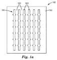
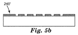
一部の実施形態では、本開示は、その1つ以上の表面(例えば主面)上にパターン化層(例えば炭素層)を有する基板を含む物品を提供する。図1a及び1bは、基板120上に配置されたパターン化層110を含む物品100の概略平面図及び概略側面図又は断面図をそれぞれ示す。パターン化層110は、パターン化層110によって覆われた領域130及び露出した、つまりパターン化層110によって覆われていない領域140を画定する。
In some embodiments, the present disclosure provides an article that includes a substrate having a patterned layer (eg, a carbon layer) on one or more surfaces (eg, a major surface) thereof. FIGS. 1 a and 1 b show a schematic top view and a schematic side view or cross-sectional view, respectively, of an
様々な実施形態では、基板は、剛性又は可撓性のものであり得る。基板は、自立性を有するのに少なくとも充分な機械的一体性を有し得る。基板は1層のみの材料で本質的に構成されてもよく、又は多層構造を有してもよい。基板は任意の形状及び厚さを有し得る。 In various embodiments, the substrate can be rigid or flexible. The substrate can have at least sufficient mechanical integrity to be self-supporting. The substrate may consist essentially of only one layer of material or may have a multilayer structure. The substrate can have any shape and thickness.
一部の実施形態では、基板は、例えばポリプロピレン(PP)などのポリオレフィン、例えばポリエチレンテレフタレート(PET)、ポリメチルメタクリレート(PMMA)などの様々なポリエステル、及びポリエチレンナフタレート(PEN)、ポリエーテルスルホン(PES)、ポリカーボネート(PC)、ポリエーテルイミド(PEI)、ポリアリレート(PAR)、ポリイミド(PI)、ポリウレタン(PU)、ポリシリコーンなどの他のポリマー、又はこれらの組み合わせなどから選択されるプラスチック基板であってよい。また、基板は、金属(例えば、Al、Cu、Ni、Ag、Au、Ti、及び/又はCr)、金属酸化物、ガラス、複合材料、紙、布地、不織布、又はこれらの組み合わせであってもよい。様々な実施形態では、基板は、PET又はPENなどの透明なポリマーフィルムを含み得る。 In some embodiments, the substrate is a polyolefin such as polypropylene (PP), various polyesters such as polyethylene terephthalate (PET), polymethyl methacrylate (PMMA), and polyethylene naphthalate (PEN), polyethersulfone ( Plastic substrate selected from PES), polycarbonate (PC), polyetherimide (PEI), polyarylate (PAR), polyimide (PI), polyurethane (PU), other polymers such as polysilicon, or combinations thereof It may be. Further, the substrate may be a metal (for example, Al, Cu, Ni, Ag, Au, Ti, and / or Cr), a metal oxide, glass, a composite material, paper, a fabric, a nonwoven fabric, or a combination thereof. Good. In various embodiments, the substrate can include a transparent polymer film, such as PET or PEN.
例示的な実施形態では、パターン化層は、任意の剥離性材料(例えば剥離性粒子)から形成されるか、又はこれらを含むことができる。一部の実施形態では、パターン化層は、元素状炭素の任意の形態若しくは種類から形成されるか、又はこれらを含むことができる。炭素層に有用な例示的な炭素としては、グラファイト、カーボンブラック、ランプブラック、又は当業者には周知の他の導電性炭素材料などの導電性炭素が挙げられる。様々な実施形態では、剥離性炭素粒子を使用してパターン化層を形成してもよい。有用な剥離性炭素粒子の例としては、HSAG300グラファイト粒子(Timcal Graphite and Carbon(Bodio,Switzerland)から入手可能)がある。他の有用な材料としては、これらに限定されるものではないが、SUPER P及びENSACO(Timcal)、並びにAsbury Carbon(Asbury,New Jersey)から入手可能なM850が挙げられる。炭素粒子はまた、多層カーボンナノチューブなどのカーボンナノチューブを含んでもよい。一部の実施形態では、パターン化層の形成に使用される炭素粒子は、0.4〜3.0のモース硬度を有してよく、最大寸法が約100マイクロメートル未満であってよい。一部の実施形態では、パターン化層は、高分子ミクロスフェア及び/又は他のミクロスフェアなどの更なる成分を含み得る。本開示は、主にパターン化炭素層を使用する実施形態に関して記載されるが、本開示の物品は、MoS2(二硫化モリブデン)、WS2(二硫化タングステン)、粘土、及びh−BN(六方晶窒化ホウ素)、ポリテトラフルオロエチレン(PTFE)、イオウ、並びにこれらの組み合わせなどの、他の剥離性材料から形成されたパターン化層を代替的又は追加的に含み得ることを理解すべきである。このように、本開示の方法は、半導体性、半金属、及び絶縁コーティングのパターニングに対応する。 In an exemplary embodiment, the patterned layer can be formed from or include any peelable material (eg, peelable particles). In some embodiments, the patterned layer can be formed from or include any form or type of elemental carbon. Exemplary carbons useful in the carbon layer include conductive carbon such as graphite, carbon black, lamp black, or other conductive carbon materials well known to those skilled in the art. In various embodiments, peelable carbon particles may be used to form the patterned layer. An example of a useful exfoliating carbon particle is HSAG300 graphite particles (available from Timcal Graphite and Carbon, Bodio, Switzerland). Other useful materials include, but are not limited to, SUPER P and ENSACO (Timcal), and M850 available from Asbury Carbon (Asbury, New Jersey). The carbon particles may also include carbon nanotubes such as multi-walled carbon nanotubes. In some embodiments, the carbon particles used to form the patterned layer may have a Mohs hardness of 0.4 to 3.0 and a maximum dimension of less than about 100 micrometers. In some embodiments, the patterned layer may include additional components such as polymeric microspheres and / or other microspheres. Although the present disclosure will be described primarily with respect to embodiments using a patterned carbon layer, the articles of the present disclosure may include MoS 2 (molybdenum disulfide), WS 2 (tungsten disulfide), clay, and h-BN ( It should be understood that patterned layers formed from other peelable materials such as hexagonal boron nitride), polytetrafluoroethylene (PTFE), sulfur, and combinations thereof may alternatively or additionally be included. is there. Thus, the disclosed method accommodates patterning of semiconducting, semi-metallic, and insulating coatings.
下記により詳細に述べるように、様々な実施形態において、パターン化層は、炭素粒子を含む乾燥組成物を塗布することにより基板上に形成することができる。本開示の目的では、「乾燥」とは、液体を含まないか又は実質的に含まないことを意味する。したがって、パターン化炭素層を形成する乾燥組成物は、液体又はペースト状ではなく、固体粒子状のものとして与えることができる。 As described in more detail below, in various embodiments, the patterned layer can be formed on the substrate by applying a dry composition comprising carbon particles. For purposes of this disclosure, “dry” means free or substantially free of liquid. Therefore, the dry composition forming the patterned carbon layer can be provided as a solid particulate form rather than a liquid or paste form.
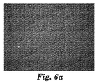
パターン化炭素層を使用する様々な実施形態では、本明細書に開示される塗布方法の結果として、パターン化炭素層は、一方で単層のグラフェンと異なり、他方でナノ結晶性グラファイトと異なる特徴的な形態を有し得る。図2は、本開示の一部の実施形態によるパターン化炭素層の走査型トンネル顕微鏡(STM)画像150である。この画像の縮尺は、正方形の画像の各辺の長さが6マイクロメートルであるようなものである。この画像は、グラファイト状炭素プレートレット160がナノ結晶性グラファイト170に包埋されている形態を示している。
In various embodiments that use a patterned carbon layer, as a result of the coating methods disclosed herein, the patterned carbon layer is different on the one hand from monolayer graphene and on the other hand from nanocrystalline graphite. May have a typical form. FIG. 2 is a scanning tunneling microscope (STM)
一部の実施形態では、パターン化層は、500マイクロメートル未満、100マイクロメートル未満、3マイクロメートル未満、1000ナノメートル未満、200ナノメートル未満、又は更には50ナノメートル未満の平均の厚さで基板上に、又は基板を覆って形成することができる。一部の実施形態では、パターン化層は、25ナノメートル〜3マイクロメートル、50ナノメートル〜1000ナノメートル、又は100ナノメートル〜500ナノメートルの範囲の平均の厚さで基板上に、又は基板を覆って形成することができる。様々な実施形態において、パターン化層は、1000ナノメートル未満、200ナノメートル未満、50ナノメートル未満、10ナノメートル未満、又は更には1ナノメートル未満の平均の厚さで基板上に形成されるカーボンナノ層であってよい。例示的な実施形態では、パターン化層は、均一な厚さを有し得る。本開示の目的では、「均一な厚さ」とは、基板の平面内で物品の所望の寸法にわたって比較的一定の厚さのコーティングを有することを意味する。この層の均一性は、例えば光学濃度計を用いた光学的評価によって評価することができる。均一性を評価するには、透過率指示値(又は反射率)を、6つの点で取り、比較することによって変動を求める。一部の実施形態では、パターン化炭素層の厚さの変動は、10%以下、5%以下、又は3%以下である。評価される波長は、層及び基板の物理的特性に依存し、コーティングの均一性を正確に評価するよう適切に選択される。例えば、通常の光条件下で視認されるコーティングは、可視光の中間点として一般に認められている、550nmなどの可視光範囲内の光波長を用いて評価される。 In some embodiments, the patterned layer has an average thickness of less than 500 micrometers, less than 100 micrometers, less than 3 micrometers, less than 1000 nanometers, less than 200 nanometers, or even less than 50 nanometers. It can be formed on or over the substrate. In some embodiments, the patterned layer is on the substrate with an average thickness in the range of 25 nanometers to 3 micrometers, 50 nanometers to 1000 nanometers, or 100 nanometers to 500 nanometers, or a substrate Can be formed. In various embodiments, the patterned layer is formed on the substrate with an average thickness of less than 1000 nanometers, less than 200 nanometers, less than 50 nanometers, less than 10 nanometers, or even less than 1 nanometer. It may be a carbon nanolayer. In an exemplary embodiment, the patterned layer can have a uniform thickness. For purposes of this disclosure, “uniform thickness” means having a relatively constant thickness of coating over the desired dimensions of the article in the plane of the substrate. The uniformity of this layer can be evaluated, for example, by optical evaluation using an optical densitometer. To evaluate the uniformity, the transmittance indication value (or reflectance) is taken at six points and the variation is obtained by comparison. In some embodiments, the variation in the thickness of the patterned carbon layer is 10% or less, 5% or less, or 3% or less. The wavelength to be evaluated depends on the physical properties of the layer and the substrate and is appropriately selected to accurately evaluate the uniformity of the coating. For example, a coating that is visible under normal light conditions is evaluated using a light wavelength in the visible light range, such as 550 nm, which is generally accepted as the midpoint of visible light.
再度、図1を参照すると、パターン化層は、層110によって覆われた領域130及び層110によって露出された領域140を画定するパターン110(例えば導電パターン)で基板上に形成され得る。一般に、パターン110は、離間したストリップ、線、パッド、格子などとして提供されてもよい。例えば、図1に示すように、パターン110は、比較的細いトレースによって結合された一連の形状(例えば、多角形、円)を含んでもよいが、バー(均一又は不均一な幅)及び/又は多角形、円形(例えば、円、楕円)のアレイなどの任意の好適な構成で提供されてもよい。代替的又は追加的に、パターン110は、例えば、正方格子、長方形(非正方)格子、又は正六角網などの、2次元メッシュを有する1つ以上の領域を含んでもよく、パターン特徴(例えば線)は、メッシュ内に囲まれた開放領域(すなわちセル)を画定する。メッシュセルの他の有用な形状としては、ランダムなセル形状、及び不規則多角形が挙げられ得る。
Referring again to FIG. 1, a patterned layer may be formed on the substrate with a pattern 110 (eg, a conductive pattern) that defines a
パターン110は、炭素層パターン110によって覆われた基板表面の合計表面積(すなわちパターン被覆表面積)に関して説明され得る。一部の実施形態では、パターン被覆表面積は、少なくとも50%、少なくとも30%、少なくとも10%、少なくとも5%、又は少なくとも1%であり得る。基板表面の残りは、パターン化されていない合計表面積である。
The
一部の実施形態では、パターンを含む特徴(例えば線)の幅は、パターンの選択によって異なり得る。例えば、パターン化特徴(例えば線の幅)は、5000マイクロメートル未満、500マイクロメートル未満、50マイクロメートル未満、25マイクロメートル未満、10マイクロメートル未満、5マイクロメートル未満、又は更には1マイクロメートル未満であり得る。一部の実施形態では、パターン化特徴(例えば線の幅)は、1〜500マイクロメートル、1〜100マイクロメートル、又は1〜50マイクロメートルの範囲である。例示的な実施形態では、特徴間の間隔は、5mm未満、1mm未満、100マイクロメートル未満、50マイクロメートル未満、又は更には10マイクロメートル未満であり得る。特徴間の間隔は、10マイクロメートル〜5mm、10マイクロメートル〜100マイクロメートル、又は10マイクロメートル〜50マイクロメートルの範囲であり得る。 In some embodiments, the width of a feature (eg, line) that includes a pattern can vary depending on the choice of pattern. For example, the patterning feature (eg, line width) is less than 5000 micrometers, less than 500 micrometers, less than 50 micrometers, less than 25 micrometers, less than 10 micrometers, less than 5 micrometers, or even less than 1 micrometer It can be. In some embodiments, the patterning feature (eg, line width) ranges from 1 to 500 micrometers, 1 to 100 micrometers, or 1 to 50 micrometers. In exemplary embodiments, the spacing between features can be less than 5 mm, less than 1 mm, less than 100 micrometers, less than 50 micrometers, or even less than 10 micrometers. The spacing between features can range from 10 micrometers to 5 mm, 10 micrometers to 100 micrometers, or 10 micrometers to 50 micrometers.
様々な実施形態において、本開示のパターン化層は、参照として本明細書に全体で組み込まれた、米国特許第6,511,701号に述べられるように形成された炭素層であってもよい。 In various embodiments, the patterned layer of the present disclosure may be a carbon layer formed as described in US Pat. No. 6,511,701, incorporated herein by reference in its entirety. .
様々な実施形態では、本開示の物品は、パターン化層を有する基板の1つ以上の表面上に形成された1つ以上の更なる層又は材料を(パターン化層に加えて)含み得る。例えば、被覆層は、パターン化層が被覆層と基板との間に存在するように基板上に配置され得る。追加的又は代替的に、物品は、1つ以上の充填材及び/又は接着剤を含み得る。好適な被覆層、充填材、及び接着剤としては、金属酸化物、塗布可能な有機物質、光学接着剤などが挙げられる。追加的又は代替的に、物品は、1つ以上のハードコート層、1つ以上の反射防止層、及び/又は1つ以上の絶縁層を含み得る。本開示による様々な構成では、基板、任意の被覆層、任意の充填材、任意の接着剤、他の任意の層などは、可視スペクトルにおいて透明又は実質的に透明である。 In various embodiments, the articles of the present disclosure may include (in addition to the patterned layer) one or more additional layers or materials formed on one or more surfaces of the substrate having the patterned layer. For example, the cover layer can be disposed on the substrate such that the patterned layer is between the cover layer and the substrate. Additionally or alternatively, the article can include one or more fillers and / or adhesives. Suitable coating layers, fillers, and adhesives include metal oxides, applicable organic materials, optical adhesives, and the like. Additionally or alternatively, the article can include one or more hardcoat layers, one or more anti-reflective layers, and / or one or more insulating layers. In various configurations according to the present disclosure, the substrate, optional covering layer, optional filler, optional adhesive, other optional layer, etc. are transparent or substantially transparent in the visible spectrum.
例示的な実施形態では、基板の表面上に又は表面を覆って配置されたパターン化層を含み得る、本開示の物品は、物品を電子用途での使用に好適にする特性を示し得る。例えば、物品は、容量性及び/又は誘導性タッチスクリーン用、特にタッチスクリーンを通して画像を見ることができるように可視光線を透過するタッチスクリーン用の検出要素として有用であり得る。この点において、本開示の物品は、透明又は実質的に透明であってもよく、パターン化炭素層は、導電性を有する物品を提供できる。 In an exemplary embodiment, an article of the present disclosure that may include a patterned layer disposed on or over the surface of the substrate may exhibit properties that make the article suitable for use in electronic applications. For example, the article can be useful as a sensing element for capacitive and / or inductive touch screens, particularly for touch screens that transmit visible light so that images can be viewed through the touch screen. In this regard, the articles of the present disclosure may be transparent or substantially transparent, and the patterned carbon layer can provide an article having conductivity.
一部の実施形態では、本開示の物品は、可視光波長にわたって比較的高い透過率を有し得る。例えば、物品の透過率(%)は、550nm又は可視波長範囲(400〜700nm)にわたって少なくとも30%、少なくとも50%、少なくとも60%、少なくとも70%、少なくとも80%、又は更には少なくとも90%であり得る。 In some embodiments, the articles of the present disclosure may have a relatively high transmittance over visible light wavelengths. For example, the transmission (%) of the article is at least 30%, at least 50%, at least 60%, at least 70%, at least 80%, or even at least 90% over the 550 nm or visible wavelength range (400-700 nm). obtain.
炭素パターン化層を使用する例示的な実施形態では、炭素パターン化層は、導電性を有する本開示の物品を提供できる。例えば、パターン化炭素層は、物品に105オーム/平方以下、104オーム/平方以下、103オーム/平方以下、又は更には102オーム/平方以下のシート抵抗を与えることができる。 In an exemplary embodiment using a carbon patterned layer, the carbon patterned layer can provide an article of the present disclosure that is electrically conductive. For example, the patterned carbon layer can give the article a sheet resistance of 10 5 ohm / square or less, 10 4 ohm / square or less, 10 3 ohm / square or less, or even 10 2 ohm / square or less.
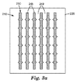
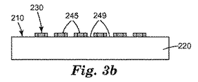
本開示は、更に、上述した物品を形成する方法に関する。図2〜4bを参照すると、この方法は、溶剤可溶性層230を所望のパターンで基板220の表面210上に又は表面210を覆って堆積させることを含み得る。次に、この方法は、第2層がパターン化溶剤可溶性層230の少なくとも一部を覆うように、第2層240を主面210の上に堆積させることを含み得る。この方法は、溶剤を主面210に塗布して溶剤可溶性層230の少なくとも一部を除去し、それによってパターン化層240’を形成することを更に含み得る。本開示の方法は、基板が静止した状態で、又は基板が適当な搬送装置(例えば、基板の移動ウェブ)によって搬送されつつある間に、前述の操作のいずれかを行うことに対応できる点が認識されるはずである。
The present disclosure further relates to a method of forming the article described above. With reference to FIGS. 2-4b, the method may include depositing a solvent
一部の実施形態では、本開示の方法は、基板の1つ以上の表面(例えば主面)上に又は表面を覆ってパターン化溶剤可溶性層を形成することを含み得る。例えば、再度、図3a〜3bを参照すると、溶剤可溶性層230は、表面210の1つ以上の第1部分245が溶剤可溶性層230によって覆われ、1つ以上の第2部分249が溶剤可溶性層230を含まないように、表面210上にパターンで形成され得る。様々な実施形態では、溶剤可溶性層230は、所望のパターン化層の逆のパターンで形成され得る。この点において、上述したパターン化層を有するように、溶剤可溶性層230は、離間したストリップ、線、パッド、格子などとして提供され得る。代替的又は追加的に、パターン化溶剤可溶性層230は、パターン化炭素層に関して上述したような2次元メッシュとして提供されてもよい。
In some embodiments, the methods of the present disclosure can include forming a patterned solvent soluble layer on or over one or more surfaces (eg, the major surface) of the substrate. For example, referring again to FIGS. 3 a-3 b, the solvent-
一般に、本開示の溶剤可溶性層は、適切な溶剤で洗浄することにより素早く除去できるように配合され得る。このように、本開示の方法は、高速で実施可能なプロセスでのパターン化層の形成に対応できる。一部の実施形態では、溶剤可溶性層は、水溶性であってもよい。様々な実施形態では、溶剤可溶性層は、水溶性インクを含み得る。例えば、溶剤可溶性層は、水溶性被膜形成ポリマーと、溶解性促進剤と、米国特許第4,895,630号に記載されるような被膜形成剤中で不溶性である固体粒子と、の組み合わせとして配合される、水溶性インクを含み得る。水溶性インクの代わりとして、又はそれに加えて、溶剤可溶性層は、ポリビニルアルコール(PVA)又はポリメタクリル酸メチル(PMMA)を含み得る。 In general, the solvent soluble layers of the present disclosure can be formulated so that they can be quickly removed by washing with a suitable solvent. As described above, the method of the present disclosure can correspond to the formation of the patterned layer in a process that can be performed at high speed. In some embodiments, the solvent soluble layer may be water soluble. In various embodiments, the solvent soluble layer can include a water soluble ink. For example, the solvent-soluble layer is a combination of a water-soluble film-forming polymer, a solubility promoter, and solid particles that are insoluble in the film-forming agent as described in US Pat. No. 4,895,630. It may contain a water-soluble ink that is formulated. As an alternative to or in addition to water-soluble inks, the solvent-soluble layer can comprise polyvinyl alcohol (PVA) or polymethyl methacrylate (PMMA).
様々な実施形態では、溶剤可溶性層は、溶剤可溶性層を含む材料を堆積させるのに好適な任意の方法又は装置を使用して基板上に形成され得る。例えば、本開示の溶剤可溶性層に好適な堆積方法には、スクリーン印刷、フレキソ印刷、活版印刷、グラビア印刷、パッド印刷、リソグラフ印刷、オフセット印刷、電子写真印刷、又はインクジェット印刷が挙げられ得る。溶剤可溶性層の堆積は、ロールツーロール法又は一部分ずつのいずれかで実施され得る。 In various embodiments, the solvent soluble layer can be formed on the substrate using any method or apparatus suitable for depositing a material comprising the solvent soluble layer. For example, suitable deposition methods for the solvent soluble layers of the present disclosure may include screen printing, flexographic printing, letterpress printing, gravure printing, pad printing, lithographic printing, offset printing, electrophotographic printing, or inkjet printing. The deposition of the solvent soluble layer can be performed either in a roll-to-roll process or in portions.
例示的な実施形態では、溶剤可溶性層は、少なくとも50nm、少なくとも100nm、少なくとも500nm、少なくとも1マイクロメートル、少なくとも2.5マイクロメートル、又は更には少なくとも5マイクロメートルの平均の厚さで基板上に形成され得る。一部の実施形態では、溶剤可溶性層は、50ナノメートル〜3マイクロメートル、又は100ナノメートル〜2.5マイクロメートルの範囲の平均の厚さで基板上に形成され得る。 In exemplary embodiments, the solvent soluble layer is formed on the substrate with an average thickness of at least 50 nm, at least 100 nm, at least 500 nm, at least 1 micrometer, at least 2.5 micrometers, or even at least 5 micrometers. Can be done. In some embodiments, the solvent soluble layer may be formed on the substrate with an average thickness in the range of 50 nanometers to 3 micrometers, or 100 nanometers to 2.5 micrometers.
一部の実施形態では、本開示の方法は、パターン化溶剤可溶性層を有する基板の表面(例えば主面)上に第2層を形成することを更に含み得る。第2層は、基板のパターン化されていない部分(すなわちパターン化溶剤可溶性層のない部分)に、直接(すなわち露出したコーティングされていない基板上に)又は間接的に(すなわち基板上に配置された1つ以上のコーティング上に)形成されてもよい。同様に、第2層は、パターン化された部分(すなわち溶剤可溶性層によって覆われた部分)に、直接(すなわち露出したコーティングされていない溶剤可溶性層上に)及び/又は間接的に(すなわち溶剤可溶性層上に配置された1つ以上のコーティング又は層上に)形成されてもよい。引き続き図3a〜5bを参照すると、例示的な実施形態では、第2層240は、第2層が基板210の第1部分245及び第2部分249を共に覆うように基板上に形成され得る。あるいは、第2層240は、第1部分245及び/又は第2部分249の1つ以上の区分のみを覆ってもよい。
In some embodiments, the methods of the present disclosure can further include forming a second layer on the surface (eg, major surface) of the substrate having the patterned solvent soluble layer. The second layer is disposed on the unpatterned portion of the substrate (ie, the portion without the patterned solvent soluble layer), directly (ie, on the exposed uncoated substrate) or indirectly (ie, on the substrate). On one or more coatings). Similarly, the second layer can be formed directly on the patterned portion (ie, the portion covered by the solvent soluble layer), directly (ie, on the exposed uncoated solvent soluble layer) and / or indirectly (ie, solvent). May be formed on one or more coatings or layers disposed on the soluble layer. With continued reference to FIGS. 3 a-5 b, in an exemplary embodiment, the
一部の実施形態では、第2層を形成することは、かなりの量の剥離性材料(例えば上述したような剥離性導電性炭素材料)を基板の表面上にバフィングすることを含み得る。本明細書で使用するところの「バフィング」とは、対象主面(例えば基板の対象主面)に垂直な圧力を、運動(例えば、回転運動、横運動、これらの組み合わせ)と組み合わせて前記主面に対して平行な平面内において作用させる任意の操作のことを指す。例示的な実施形態では、剥離性材料は、粒子、並びに場合により高分子ミクロスフェア及び/又は他のミクロスフェアなどの更なる成分を含む乾燥組成物として塗布することができる。したがって、塗布される組成物は、液体又はペースト状ではなく、固体粒子状のものとして与えられる。炭素粒子を使用する実施形態では、炭素粒子は、炭素の任意の形態又は種類であってもよい。例示的な炭素には、導電性炭素、例えばグラファイト、カーボンブラック、ランプブラック、又は他の導電性炭素材料が挙げられる。有用な剥離性炭素粒子の例としては、HSAG300グラファイト粒子(Timcal Graphite and Carbon(Bodio,Switzerland)から入手可能)がある。他の有用な材料としては、これらに限定されるものではないが、SUPER P及びENSACO(Timcal)、並びにAsbury Carbon(Asbury,New Jersey)より入手可能なM850が挙げられる。炭素粒子は、多層カーボンナノチューブを含むカーボンナノチューブであってもよく又はこれを含んでもよい。炭素粒子は、0.4〜3.0のモース硬度を有し、最大寸法は約100マイクロメートル未満であり得る。 In some embodiments, forming the second layer can include buffing a substantial amount of a peelable material (eg, a peelable conductive carbon material as described above) onto the surface of the substrate. As used herein, “buffing” refers to a pressure that is perpendicular to a target main surface (eg, a target main surface of a substrate) combined with movement (eg, rotational movement, lateral movement, a combination thereof). It refers to any operation that acts in a plane parallel to the surface. In an exemplary embodiment, the peelable material can be applied as a dry composition comprising particles and optionally further components such as polymeric microspheres and / or other microspheres. Therefore, the composition to be applied is given as solid particles, not liquid or paste. In embodiments that use carbon particles, the carbon particles may be any form or type of carbon. Exemplary carbons include conductive carbon, such as graphite, carbon black, lamp black, or other conductive carbon materials. An example of a useful exfoliating carbon particle is HSAG300 graphite particles (available from Timcal Graphite and Carbon, Bodio, Switzerland). Other useful materials include, but are not limited to, SUPER P and ENSACO (Timcal), and M850 available from Asbury Carbon (Asbury, New Jersey). The carbon particles may be or may include carbon nanotubes including multi-walled carbon nanotubes. The carbon particles can have a Mohs hardness of 0.4 to 3.0 and a maximum dimension can be less than about 100 micrometers.
第2層のバフィングは、表面に乾燥粒子を塗布するのに適した、当該技術分野では周知の任意のバフィング装置(例えば、電動サンダー、電動バファー、オービタルサンダー、ランダムオービタルサンダー)を使用するか、又は手動で(すなわち手で)行うことができる。例示的なバフィング装置は、対象表面に垂直な圧力を作用させると共に前記対象表面に対して平行な平面内で回転するように構成することができるモーター駆動式バフィングアプリケーター(例えば、ディスク、ホイール)を含み得る。バフィングアプリケーターは、バフィング操作の間に対象表面と接触するか、又は接触することを意図したバフィング表面を有し得る。一部の実施形態では、バフィング表面は、金属、ポリマー、ガラス、発泡材(例えば独立気泡型発泡材)、布地、紙、ゴム、又はこれらの組み合わせを含み得る。様々な実施形態において、バフィング表面は、表面に粒子を塗布するための任意の適当な材料で形成することができるアプリケーターパッドを含み得る。アプリケーターパッドは、例えば、織布若しくは不織布又はセルロース材料で形成することができる。アプリケーターパッドは、独立気泡型又は開放気泡型の発泡材料で形成することもできる。他の場合では、アプリケーターパッドは、ブラシ、又はナイロン若しくはポリウレタン製の毛の配列で形成することができる。アプリケーターパッドは、毛、布地、発泡材、及び/又は他の構造体を含むかによらず、塗布される組成物の粒子が入り込んでアプリケーターパッドによって運び去られるようなトポグラフィーを有し得る。 The second layer buffing uses any buffing device known in the art suitable for applying dry particles to the surface (eg, electric sander, electric buffer, orbital sander, random orbital sander), Or it can be done manually (ie by hand). An exemplary buffing device includes a motor driven buffing applicator (eg, disc, wheel) that can be configured to exert a pressure normal to the target surface and rotate in a plane parallel to the target surface. May be included. The buffing applicator may have a buffing surface that contacts or is intended to contact the target surface during the buffing operation. In some embodiments, the buffing surface can include metal, polymer, glass, foam (eg, closed cell foam), fabric, paper, rubber, or combinations thereof. In various embodiments, the buffing surface can include an applicator pad that can be formed of any suitable material for applying particles to the surface. The applicator pad can be formed of, for example, a woven or non-woven fabric or a cellulosic material. The applicator pad can also be formed of a closed cell or open cell foam material. In other cases, the applicator pad can be formed of a brush or an array of hair made of nylon or polyurethane. The applicator pad may have a topography that allows particles of the composition to be applied to enter and be carried away by the applicator pad, regardless of whether it includes bristles, fabrics, foams, and / or other structures.
一部の実施形態では、バフィングアプリケーターは、対象表面に対して平行なパターンで動くと共に、対象表面に垂直な回転軸を中心として回転するように構成することができる。パターンは、単純なオービタル運動又はランダムなオービタル運動を含み得る。バフィングアプリケーターの回転は、毎分100オービットの高さ、毎分1,000オービットの高さ、又は更には毎分10,000オービットの高さで行うことができる。バフィングアプリケーターは、少なくとも0.1g/cm2、少なくとも1g/cm2、少なくとも10g/cm2、少なくとも20g/cm2(少なくとも0.0098kPa、少なくとも0.098kPa、少なくとも0.98kPa、少なくとも2.0kPa)、又は更には少なくとも30g/cm2(少なくとも2.9kPa)の圧力で、対象表面に垂直な方向で適用され得る。 In some embodiments, the buffing applicator can be configured to move in a pattern parallel to the target surface and to rotate about an axis of rotation perpendicular to the target surface. The pattern can include simple orbital motion or random orbital motion. The buffing applicator can be rotated at a height of 100 orbits per minute, 1,000 orbits per minute, or even 10,000 orbits per minute. The buffing applicator is at least 0.1 g / cm 2 , at least 1 g / cm 2 , at least 10 g / cm 2 , at least 20 g / cm 2 (at least 0.0098 kPa, at least 0.098 kPa, at least 0.98 kPa, at least 2.0 kPa) Or even at a pressure of at least 30 g / cm 2 (at least 2.9 kPa) and in a direction perpendicular to the surface of interest.
第2層は、多くの方法で基板の表面上に又は表面を覆って形成され得る。一手法では、第2層の形成に使用される組成物を最初に表面に直接塗布し、次いでバフィングアプリケーターを組成物及び表面に接触させることができる。別の手法では、組成物を最初にバフィング装置のバフィング表面に塗布し、次いで粒子が装填されたバフィング表面を基板の表面と接触させることができる。更に別の手法では、組成物の一部を表面に直接塗布し、組成物の別の部分をバフィング装置のバフィング表面に塗布した後、粒子が装填されたバフィング表面を表面及び組成物の残りの部分と接触させることができる。 The second layer can be formed on or over the surface of the substrate in a number of ways. In one approach, the composition used to form the second layer can be first applied directly to the surface, and then a buffing applicator is contacted with the composition and the surface. In another approach, the composition can be first applied to the buffing surface of the buffing device and then the buffing surface loaded with particles can be brought into contact with the surface of the substrate. In yet another approach, a portion of the composition is applied directly to the surface, another portion of the composition is applied to the buffing surface of the buffing device, and the buffing surface loaded with particles is then applied to the surface and the rest of the composition. Can be in contact with the part.
一部の実施形態では、本開示のバフィング操作を用いて高品質の薄層(例えばカーボンナノ層)を基板の表面上に又は表面を覆って製造することができる。バフィングされた層の厚さは、バフィング時間を調節することによって調節することができる。一般的にコーティングの厚さは、特定の急速な初期の増大の後、バフィング時間と共に直線的に増大し得る。第2層のコーティング厚さは、バフィング操作において使用される組成物の量を調節することによって調節することもできる。 In some embodiments, high quality thin layers (eg, carbon nanolayers) can be produced on or over the surface of the substrate using the buffing operations of the present disclosure. The thickness of the buffed layer can be adjusted by adjusting the buffing time. In general, the coating thickness may increase linearly with buffing time after a certain rapid initial increase. The coating thickness of the second layer can also be adjusted by adjusting the amount of composition used in the buffing operation.
本明細書に述べられるバフィングを使用することによって、均一な厚さ、高い透明度、及び適当なシート抵抗を有する高品質、低コストの炭素の層を製造することができる。更に、前述したように、本開示のバフコーティングプロセスによって製造される炭素層は、一方で単層のグラフェンと異なり、他方でナノ結晶性グラファイトと異なる特徴的な形態を有し得る。例えば、本開示の炭素層は、グラファイト状炭素プレートレットがナノ結晶性グラファイト中に包埋された形態を有し得る。 By using the buffing described herein, a high quality, low cost carbon layer with uniform thickness, high transparency, and appropriate sheet resistance can be produced. Furthermore, as previously mentioned, the carbon layer produced by the buff coating process of the present disclosure may have a characteristic morphology that is different from single-layer graphene on the one hand and from nanocrystalline graphite on the other hand. For example, the carbon layer of the present disclosure may have a form in which graphitic carbon platelets are embedded in nanocrystalline graphite.
様々な実施形態では、本明細書に記載のバフィングプロセスは、第2層が基板のパターン化されていない部分と溶剤可溶性層の特徴の上面及び側面とに実質的にぴったり一致するように、第2層を基板及びパターン化溶剤可溶性層の全露出面上に形成することができる。更に、このようにぴったり一致する第2層は、溶剤可溶性層を損傷する(例えばパターン特徴を変化させる)ことなく形成され得る。この点において、驚いたことに、本開示のバフィング方法は、溶剤可溶性層の厚さに比べて大きな毛、布地、及び/又は他の表面構造を含む、バフィングアプリケーターパッドの高速反復運動を伴い得るが、溶剤可溶性層を摩耗又は損傷しないことが分かった。したがって、犠牲溶剤可溶性層の物理的一体性は、炭素層形成プロセスにわたって実質的に維持され、鮮明なエッジ解像力を示すパターン化層をもたらすことができる。 In various embodiments, the buffing process described herein may be such that the second layer substantially conforms to the unpatterned portion of the substrate and the top and sides of the features of the solvent soluble layer. Two layers can be formed on all exposed surfaces of the substrate and the patterned solvent soluble layer. Further, such a closely matching second layer can be formed without damaging the solvent soluble layer (eg, changing pattern features). In this regard, surprisingly, the buffing method of the present disclosure can involve high-speed repetitive motion of the buffing applicator pad, including bristles, fabrics, and / or other surface structures that are larger than the thickness of the solvent-soluble layer. However, it has been found that it does not wear or damage the solvent soluble layer. Thus, the physical integrity of the sacrificial solvent soluble layer can be substantially maintained throughout the carbon layer formation process, resulting in a patterned layer that exhibits sharp edge resolution.
例示的な実施形態では、第2層の基板に対する固着性は、バフィング操作の前、その間、又はその後で、層の接着性が向上するような温度にまで基板を加熱することによって促進することができる。基板への熱入力の例示的な方法としては、オーブン加熱、ヒートランプ加熱(例えば赤外線)、又は基板と接触した加熱板が挙げられる。 In an exemplary embodiment, the adhesion of the second layer to the substrate may be promoted by heating the substrate to a temperature such that the adhesion of the layer is improved before, during or after the buffing operation. it can. Exemplary methods of heat input to the substrate include oven heating, heat lamp heating (eg, infrared), or a heating plate in contact with the substrate.
様々な実施形態では、第2層は、米国特許第6,511,701号に記載される方法に基づいて基板上に堆積され得る。 In various embodiments, the second layer can be deposited on the substrate based on the method described in US Pat. No. 6,511,701.
一部の実施形態では、第2層の形成後に、本開示の方法は、基板から溶剤可溶性層を除去してパターン化層を形成することを含み得る。一般に、溶剤可溶性層の除去は、溶剤によって溶剤可溶性層を溶解させるか、ないしは別の方法で基板から除去するように、溶剤を基板に塗布することを含み得る。溶剤の塗布は、溶剤浸漬、すすぎ、洗浄、噴霧、はけ塗りなどのいずれか又は全てを含み得る。溶剤の塗布は、基板及び溶剤の一方又は両方のかき混ぜ、振動、振盪、撹拌などのいずれか又は全てによって向上され得る。様々な実施形態では、前述の除去プロセスは、溶剤可溶性層の除去に加えて、除去時に溶剤可溶性層に付着している第2層の部分も除去し得る。驚いたことに、かつ有利なことに、本開示の溶剤除去プロセスは、パターン化層を損傷又は劣化させないことが分かった。すなわち、溶剤可溶性層及びそれに付着する第2層の任意の部分の除去後に得られるパターン化層は、高品質であり、優れたエッジ解像力を示す。 In some embodiments, after forming the second layer, the disclosed method can include removing the solvent soluble layer from the substrate to form a patterned layer. In general, removal of the solvent soluble layer may include applying the solvent to the substrate such that the solvent soluble layer is dissolved by the solvent or otherwise removed from the substrate. Solvent application may include any or all of solvent immersion, rinsing, cleaning, spraying, brushing, and the like. Solvent application can be improved by any or all of agitation, shaking, shaking, stirring, etc. of one or both of the substrate and solvent. In various embodiments, the removal process described above may remove portions of the second layer that are attached to the solvent-soluble layer during removal, in addition to removing the solvent-soluble layer. Surprisingly and advantageously, it has been found that the solvent removal process of the present disclosure does not damage or degrade the patterned layer. That is, the patterned layer obtained after removal of any part of the solvent-soluble layer and the second layer adhering thereto is of high quality and exhibits excellent edge resolution.
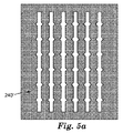
図5a〜5bは、溶剤可溶性層230及びそれに付着する第2層240の部分を基板220から除去した後の基板220の概略平面図及び概略側面図をそれぞれ示す。図示するように、犠牲溶剤可溶性層230によって形成されたパターン化特徴のほぼ逆である層パターン240’が、基板220の表面210上に形成され得る。
FIGS. 5 a-5 b show a schematic plan view and a schematic side view, respectively, of the
本開示の物品は、第2層が炭素層である実施形態において、例えば、検出要素としてパターン化された透明な導電体を用いるタッチセンシティブオーバレイとして使用され得る。これらには、ディスクリートマトリックスタッチセンサ(米国特許第6,813,957号、同第6,762,752号、同第6,188,391号、同第5,844,506号、同第5,386,219号、及び同第5,007,085号、並びに国際公開第01/27868号、同第01/100074号、及び同第01/52416号に開示されるものなど)、ディスクリートバーセンサ(米国特許第5,650,597号及び米国特許出願公開第2003/0103043号に開示されるものなど)、ディスクリートパッドセンサ(米国特許第4,789,767号に開示されるものなど)、及び他のディスクリート検出要素センサ、並びに導通パターン化検出層センサ(米国特許第4,198,539号に開示されるものなど)が挙げられる。これらの種類のセンサは、容量型、投影型、及び/又は誘導型検出技術において有利に使用されることができ、手持ち式装置(例えば、パームトップコンピュータ、電子手帳、携帯電話、音楽プレーヤなど)、タブレットコンピュータ、カーナビディスプレイ、タッチ入力モニタ、公開情報キオスク、現金自動預払機、ゲーム及びエンタテインメント装置などを含む、オンスクリーン入力から恩恵を受ける様々な用途で使用されることができる。 The article of the present disclosure can be used in embodiments where the second layer is a carbon layer, for example, as a touch-sensitive overlay using a patterned transparent conductor as the sensing element. These include discrete matrix touch sensors (US Pat. Nos. 6,813,957, 6,762,752, 6,188,391, 5,844,506, 386,219, and 5,007,085, and those disclosed in WO01 / 27868, 01/100074, and 01/52416), discrete bar sensors ( U.S. Pat. No. 5,650,597 and U.S. Patent Application Publication No. 2003/0103043), Discrete Pad Sensors (such as those disclosed in U.S. Pat. No. 4,789,767), and others Discrete sensing element sensors as well as conductive patterned sensing layer sensors (such as those disclosed in US Pat. No. 4,198,539). It is below. These types of sensors can be advantageously used in capacitive, projection, and / or inductive detection technologies, and handheld devices (eg, palmtop computers, electronic notebooks, cell phones, music players, etc.) Can be used in a variety of applications that benefit from on-screen input, including tablet computers, car navigation displays, touch input monitors, public information kiosks, automated teller machines, games and entertainment devices, and the like.
本開示の動作を以下の詳細な実施例に関して更に説明する。これらの実施例は、様々な具体的かつ好ましい実施形態及び技術を更に例示するために与えられるものである。しかしながら、本開示の範囲内で多くの変更及び改変がなされ得ることは理解されるべきである。 The operation of the present disclosure will be further described with respect to the following detailed examples. These examples are given to further illustrate various specific and preferred embodiments and techniques. However, it should be understood that many variations and modifications may be made within the scope of the present disclosure.
(実施例1)
75マイクロメートル厚のPET基板(Cadillac Plastics,Inc.(Toronto,Canada)から入手したMelinex(登録商標)Polyester Film 393)膜の表面上に、標準的なフレキソ技術を使用して20フィート/分(約6.1メートル/分)の速度で水溶性インクパターンを印刷した。ローラーに取り付けたゴム製のスタンプは、(1〜5ミリメートル)寸法の特徴及び間隙を有した。水溶性インクは、約250cPの粘度を有し、概ね米国特許第4,895,630号に記載されるような組成物から構成された。
Example 1
A 75 micrometer thick PET substrate (Melinex® Polyester Film 393) obtained from Cadillac Plastics, Inc. (Toronto, Canada) on the surface of a film using standard flexo technology at 20 feet / minute ( A water-soluble ink pattern was printed at a speed of about 6.1 meters / minute). The rubber stamp attached to the roller had (1-5 millimeters) dimensional features and gaps. The water-soluble ink had a viscosity of about 250 cP and was generally composed of a composition as described in US Pat. No. 4,895,630.
水溶性インクパターンの印刷後、グラファイト粉末(TIMCAL Ltd.(Switzerland)から入手したTIMREX(登録商標)HSAG 300)を約20秒間バフィングすることにより、印刷されたPET基板被膜層の8インチ×11インチ(約20.3センチメートル×27.9センチメートル)区画を炭素層でコーティングした。グラファイト粉末のバフィングは、概ね米国特許第6,511,701号に記載されるようなオービタル仕上げサンダー(Makita USA,Inc.(La Mirada,California)から入手したModel BO4900V Finishing Sander)に取り付けたペイントパッド(Shur−Line(Huntersville,North Carolina)から入手したShur−Line(登録商標)ペイントパッド)を使用して達成した。 After printing the water-soluble ink pattern, the printed PET substrate coating layer is 8 inches × 11 inches by buffing graphite powder (TIMREX® HSAG 300 obtained from TIMCAL Ltd. (Switzerland)) for about 20 seconds. The compartment (about 20.3 cm x 27.9 cm) was coated with a carbon layer. Graphite powder buffing is generally applied to a paint pad attached to an orbital finish sander (Model BO4900V Finishing Sander obtained from Makita USA, Inc. (La Mirada, Calif.)) As described in US Pat. No. 6,511,701. (Shur-Line® paint pad obtained from Shur-Line (Huntersville, North Carolina)).
驚いたことに、バフィングは、インクパターンを明らかに損なうことはなかった。次に、炭素コーティングした物品を、水を使用してペーパータオルで優しく拭き取ることにより洗浄した。直ちに、水溶性インクパターン上の炭素コーティング領域を除去し、水溶性インクがない部分の炭素コーティング領域は無傷で残した。これにより、水溶性インク適用範囲の逆パターンを有する、非常に明確なエッジを備えた、PET基板上のパターン化炭素コーティングが生じた。こうして、驚くほど簡単にPET上のパターン化炭素コーティングを得た。 Surprisingly, the buffing did not apparently damage the ink pattern. The carbon coated article was then washed by gently wiping with a paper towel using water. Immediately, the carbon coating area on the water-soluble ink pattern was removed, and the carbon coating area where there was no water-soluble ink was left intact. This resulted in a patterned carbon coating on the PET substrate with a very clear edge with a reverse pattern of water-soluble ink coverage. Thus, a patterned carbon coating on PET was obtained surprisingly easily.
パターンの電気シート抵抗を手持ち式2プローブメーターで測定し、103Ω/[]未満を検出した。 The electrical sheet resistance of the pattern was measured with a hand-held 2-probe meter, and less than 10 3 Ω / [] was detected.
(実施例2)
実施例2は、水溶性インクで印刷されたPET基板を、Magentaミクロスフェア(Tartan Color & Chemicals(Ontario,Canada)から入手したMP−MG5518)と15:85の重量比で混合したグラファイト粉末(TIMREX(登録商標)HSAG 300)を使用してバフィングした以外は、実施例1と同じ方法で調製した。
(Example 2)
Example 2 is a graphite powder (TIMREX) obtained by mixing a PET substrate printed with water-soluble ink with Magenta microspheres (MP-MG5518 obtained from Tartan Color & Chemicals, Ontario, Canada) at a weight ratio of 15:85. (Registered trademark) HSAG 300) was used in the same manner as in Example 1 except that buffing was performed.
実施例1の場合と同様に、バフィングは、水溶性インクパターンを明らかに損なうことはなかった。得られたパターンの特徴の幅は、1ミリメートル〜5ミリメートルの範囲であった。 As in Example 1, buffing did not clearly impair the water-soluble ink pattern. The resulting pattern feature widths ranged from 1 millimeter to 5 millimeters.
パターンの電気シート抵抗を手持ち式2プローブメーターで測定し、約104オーム/[]を検出した。 The electrical sheet resistance of the pattern was measured with a hand-held 2-probe meter and detected approximately 10 4 ohm / [].
(実施例3)
実施例3は、水溶性インクパターンを約5mmの特徴の間隔及び約40マイクロメートルの特徴の幅で印刷した以外は、実施例2と同じ方法で調製した。バフィング後、炭素コーティングした物品を水で洗浄し、パターン化炭素コーティングを現出させた。水溶性インクパターンの印刷後及び洗浄後の試料の8倍の倍率での光学顕微鏡写真を図6A及び6Bにそれぞれ示す。水溶性インクパターンの印刷後及び洗浄後の試料の100倍の倍率での光学顕微鏡写真を図7A及び7Bにそれぞれ示す。パターン化炭素コーティングの品質は、水溶性インクパターンの品質に詳細に従うことを観察した。
(Example 3)
Example 3 was prepared in the same manner as Example 2, except that a water-soluble ink pattern was printed with a feature spacing of about 5 mm and a feature width of about 40 micrometers. After buffing, the carbon coated article was washed with water to reveal a patterned carbon coating. Optical micrographs at 8 × magnification of the sample after printing and washing the water-soluble ink pattern are shown in FIGS. 6A and 6B, respectively. FIGS. 7A and 7B show optical micrographs at 100 × magnification of the sample after printing and washing the water-soluble ink pattern, respectively. It was observed that the quality of the patterned carbon coating closely follows the quality of the water-soluble ink pattern.
(実施例4)
グラファイト粉末の代わりに二硫化モリブデン粉末(MoS2、6マイクロメートルの平均粒度、Rose Mill(Hartford,CT)から入手)をPET基板上にバフィングした以外は、実施例1の方法を繰り返した。印刷されたインクパターンをMoS2粉末でコーティングした後、非常に均一なMoS2層を観察した。水で洗浄後、コーティングされたPETは、約40マイクロメートル幅のパターン化されたMoS2の線を生じた。
Example 4
The method of Example 1 was repeated except that molybdenum disulfide powder (MoS 2 , average particle size of 6 micrometers, obtained from Rose Mill, Hartford, CT) was buffed onto the PET substrate instead of graphite powder. After coating the printed ink pattern with MoS 2 powder, a very uniform MoS 2 layer was observed. After washing with water, the coated PET produced a patterned MoS 2 line about 40 micrometers wide.
(実施例5)
グラファイト粉末の代わりに六方晶窒化ホウ素粉末(h−BN、5マイクロメートルの平均粒度、M.K.Impex Corporation(Mississauga,Canada)から入手)をPET基板上にバフィングした以外は、実施例1の方法を繰り返した。水で洗浄後、コーティングされたPETは、約40マイクロメートル幅のパターン化されたh−BNのトレースを生じた。
(Example 5)
Example 1 except that hexagonal boron nitride powder (h-BN, 5 micrometer average particle size, obtained from MK Impex Corporation (Mississauga, Canada)) was buffed on the PET substrate instead of graphite powder. The method was repeated. After washing with water, the coated PET yielded a patterned h-BN trace about 40 micrometers wide.
Claims (14)
前記基板の前記表面上に又は前記表面を覆って溶剤可溶性層をパターンで形成する工程であって、前記パターンが、前記溶剤可溶性層によって覆われる、前記表面の1つ以上の第1部分と、前記溶剤可溶性層のない、前記表面の1つ以上の第2部分とを画定する、工程と、
前記第1部分の少なくとも1つ及び前記第2部分の少なくとも1つの上に、又は前記第1部分の少なくとも1つ及び前記第2部分の少なくとも1つを覆って第2層を形成する工程であって、前記第2層を形成する工程が、前記第1部分の少なくとも1つ及び前記第2部分の少なくとも1つの上に、又は前記第1部分の少なくとも1つ及び前記第2部分の少なくとも1つを覆って剥離性材料をバフィングすることを含む、工程と、
前記基板に溶剤を塗布することによって前記溶剤可溶性層を除去し、それによってパターン化層を形成する工程と、を含む、物品を形成する方法。 Preparing a substrate having a surface;
Forming a solvent-soluble layer in a pattern on or over the surface of the substrate, wherein the pattern is covered by the solvent-soluble layer; and one or more first portions of the surface; Defining one or more second portions of the surface without the solvent soluble layer;
Forming a second layer on at least one of the first part and at least one of the second part or covering at least one of the first part and at least one of the second part. And forming the second layer on at least one of the first portion and at least one of the second portion, or at least one of the first portion and at least one of the second portion. Buffing a peelable material over the substrate, and
Removing the solvent-soluble layer by applying a solvent to the substrate, thereby forming a patterned layer.
前記基板の前記表面上に又は前記表面を覆って溶剤可溶性層をパターンで形成する工程であって、前記パターンが、前記溶剤可溶性層によって覆われる、前記表面の1つ以上の第1部分と、前記溶剤可溶性層のない、前記表面の1つ以上の第2部分とを画定する、工程と、
前記第1部分の少なくとも1つ及び前記第2部分の少なくとも1つの上に、又は前記第1部分の少なくとも1つ及び前記第2部分の少なくとも1つを覆って炭素層を形成する工程であって、前記炭素層を形成する工程が、前記第1部分の少なくとも1つ及び前記第2部分の少なくとも1つの上に、又は前記第1部分の少なくとも1つ及び前記第2部分の少なくとも1つを覆って導電性炭素材料をバフィングすることを含む、工程と、
前記基板に溶剤を塗布することによって前記溶剤可溶性層を除去し、それによってパターン化炭素層を形成する工程と、を含む、方法。 Preparing a substrate having a surface;
Forming a solvent-soluble layer in a pattern on or over the surface of the substrate, wherein the pattern is covered by the solvent-soluble layer; and one or more first portions of the surface; Defining one or more second portions of the surface without the solvent soluble layer;
Forming a carbon layer on at least one of the first part and at least one of the second part, or covering at least one of the first part and at least one of the second part, Forming the carbon layer over at least one of the first portion and at least one of the second portion, or covering at least one of the first portion and at least one of the second portion. Buffing the conductive carbon material, and
Removing the solvent soluble layer by applying a solvent to the substrate, thereby forming a patterned carbon layer.
Applications Claiming Priority (3)
| Application Number | Priority Date | Filing Date | Title |
|---|---|---|---|
| US201261663097P | 2012-06-22 | 2012-06-22 | |
| US61/663,097 | 2012-06-22 | ||
| PCT/US2013/044921 WO2013191939A1 (en) | 2012-06-22 | 2013-06-10 | Methods for patterning coatings |
Publications (2)
| Publication Number | Publication Date |
|---|---|
| JP2015530630A true JP2015530630A (en) | 2015-10-15 |
| JP2015530630A5 JP2015530630A5 (en) | 2016-06-02 |
Family
ID=49769222
Family Applications (1)
| Application Number | Title | Priority Date | Filing Date |
|---|---|---|---|
| JP2015518434A Ceased JP2015530630A (en) | 2012-06-22 | 2013-06-10 | Coating patterning method |
Country Status (5)
| Country | Link |
|---|---|
| US (1) | US20150118457A1 (en) |
| EP (1) | EP2864999A4 (en) |
| JP (1) | JP2015530630A (en) |
| CN (1) | CN104471674A (en) |
| WO (1) | WO2013191939A1 (en) |
Families Citing this family (8)
| Publication number | Priority date | Publication date | Assignee | Title |
|---|---|---|---|---|
| WO2015047572A1 (en) | 2013-09-24 | 2015-04-02 | 3M Innovative Properties Company | Transferable transparent conductive patterns and display stack materials |
| KR101668817B1 (en) * | 2014-09-11 | 2016-10-25 | 주식회사 엘엠에스 | Graphene structure with enhanced electrical property |
| CN105415215B (en) * | 2015-11-06 | 2017-11-24 | 富耐克超硬材料股份有限公司 | A kind of super hard abrasive ordered arrangement method |
| US9793132B1 (en) * | 2016-05-13 | 2017-10-17 | Applied Materials, Inc. | Etch mask for hybrid laser scribing and plasma etch wafer singulation process |
| WO2018175022A1 (en) * | 2017-03-22 | 2018-09-27 | 3M Innovative Properties Company | Buff-coated article and method of making the same |
| JP2018180168A (en) * | 2017-04-07 | 2018-11-15 | ホヤ レンズ タイランド リミテッドHOYA Lens Thailand Ltd | Method for manufacturing optical member with processed pattern formed thereon |
| CN108330434A (en) * | 2018-01-11 | 2018-07-27 | 广东欧珀移动通信有限公司 | Plank and preparation method, shell, electronic equipment |
| TWI751863B (en) * | 2020-12-28 | 2022-01-01 | 新唐科技股份有限公司 | Semiconductor structure |
Citations (9)
| Publication number | Priority date | Publication date | Assignee | Title |
|---|---|---|---|---|
| JPH05327178A (en) * | 1991-03-28 | 1993-12-10 | Unitika Ltd | Continuous manufacture of transparent conductive board |
| JP2003532528A (en) * | 2000-05-09 | 2003-11-05 | スリーエム イノベイティブ プロパティズ カンパニー | Coatings and methods |
| JP2004053955A (en) * | 2002-07-19 | 2004-02-19 | Mitsubishi Chemicals Corp | Method for forming thin film on mask for prescribing magnetization pattern shape and mask for prescribing magnetization pattern shape, as well as method for removing surplus thin film of the mask |
| JP2005005721A (en) * | 2003-06-12 | 2005-01-06 | Samsung Electronics Co Ltd | Wiring board for semiconductor package, its producing process and semiconductor package utilizing it |
| JP2005191526A (en) * | 2003-08-26 | 2005-07-14 | Sony Internatl Europ Gmbh | Method for patterning organic material or combination of organic and inorganic material |
| JP2007081409A (en) * | 2005-09-15 | 2007-03-29 | Samsung Electro-Mechanics Co Ltd | Printed circuit board having fine pattern and method for manufacturing the same |
| JP2010050431A (en) * | 2008-07-25 | 2010-03-04 | Hokkaido Univ | Method of manufacturing photoresist pattern |
| JP2010253813A (en) * | 2009-04-24 | 2010-11-11 | Nissha Printing Co Ltd | Mat electrically conductive nano-fiber sheet and method of manufacturing the same |
| JP2012079257A (en) * | 2010-10-06 | 2012-04-19 | Dic Corp | Transparent conductive film laminate using double-coated adhesive sheet and touch panel device |
Family Cites Families (9)
| Publication number | Priority date | Publication date | Assignee | Title |
|---|---|---|---|---|
| GB1423952A (en) * | 1973-06-26 | 1976-02-04 | Oike & Co | Process for preparing a metallized resin film for condenser element |
| US4895630A (en) * | 1985-08-28 | 1990-01-23 | W. H. Brady Co. | Rapidly removable undercoating for vacuum deposition of patterned layers onto substrates |
| US6221562B1 (en) * | 1998-11-13 | 2001-04-24 | International Business Machines Corporation | Resist image reversal by means of spun-on-glass |
| US20070026205A1 (en) * | 2005-08-01 | 2007-02-01 | Vapor Technologies Inc. | Article having patterned decorative coating |
| KR20070068909A (en) * | 2005-12-27 | 2007-07-02 | 주식회사 하이닉스반도체 | Method of fabricating photo mask using reverse photoresist pattern |
| US7875219B2 (en) * | 2007-10-04 | 2011-01-25 | Nanotek Instruments, Inc. | Process for producing nano-scaled graphene platelet nanocomposite electrodes for supercapacitors |
| JP5112380B2 (en) * | 2009-04-24 | 2013-01-09 | 信越化学工業株式会社 | Pattern formation method |
| JP5247936B2 (en) * | 2009-07-23 | 2013-07-24 | ダウ コーニング コーポレーション | Inversion pattern forming method and material |
| US8288271B2 (en) * | 2009-11-02 | 2012-10-16 | International Business Machines Corporation | Method for reworking antireflective coating over semiconductor substrate |
-
2013
- 2013-06-10 EP EP13806808.5A patent/EP2864999A4/en not_active Withdrawn
- 2013-06-10 US US14/407,480 patent/US20150118457A1/en not_active Abandoned
- 2013-06-10 JP JP2015518434A patent/JP2015530630A/en not_active Ceased
- 2013-06-10 CN CN201380032257.9A patent/CN104471674A/en active Pending
- 2013-06-10 WO PCT/US2013/044921 patent/WO2013191939A1/en active Application Filing
Patent Citations (9)
| Publication number | Priority date | Publication date | Assignee | Title |
|---|---|---|---|---|
| JPH05327178A (en) * | 1991-03-28 | 1993-12-10 | Unitika Ltd | Continuous manufacture of transparent conductive board |
| JP2003532528A (en) * | 2000-05-09 | 2003-11-05 | スリーエム イノベイティブ プロパティズ カンパニー | Coatings and methods |
| JP2004053955A (en) * | 2002-07-19 | 2004-02-19 | Mitsubishi Chemicals Corp | Method for forming thin film on mask for prescribing magnetization pattern shape and mask for prescribing magnetization pattern shape, as well as method for removing surplus thin film of the mask |
| JP2005005721A (en) * | 2003-06-12 | 2005-01-06 | Samsung Electronics Co Ltd | Wiring board for semiconductor package, its producing process and semiconductor package utilizing it |
| JP2005191526A (en) * | 2003-08-26 | 2005-07-14 | Sony Internatl Europ Gmbh | Method for patterning organic material or combination of organic and inorganic material |
| JP2007081409A (en) * | 2005-09-15 | 2007-03-29 | Samsung Electro-Mechanics Co Ltd | Printed circuit board having fine pattern and method for manufacturing the same |
| JP2010050431A (en) * | 2008-07-25 | 2010-03-04 | Hokkaido Univ | Method of manufacturing photoresist pattern |
| JP2010253813A (en) * | 2009-04-24 | 2010-11-11 | Nissha Printing Co Ltd | Mat electrically conductive nano-fiber sheet and method of manufacturing the same |
| JP2012079257A (en) * | 2010-10-06 | 2012-04-19 | Dic Corp | Transparent conductive film laminate using double-coated adhesive sheet and touch panel device |
Also Published As
| Publication number | Publication date |
|---|---|
| EP2864999A1 (en) | 2015-04-29 |
| US20150118457A1 (en) | 2015-04-30 |
| CN104471674A (en) | 2015-03-25 |
| WO2013191939A1 (en) | 2013-12-27 |
| EP2864999A4 (en) | 2016-03-09 |
Similar Documents
| Publication | Publication Date | Title |
|---|---|---|
| JP2015530630A (en) | Coating patterning method | |
| Sreenilayam et al. | Advanced materials of printed wearables for physiological parameter monitoring | |
| Ryu et al. | Raman spectroscopy of lithographically patterned graphene nanoribbons | |
| US9668333B2 (en) | Electrically conductive article with high optical transmission | |
| Vernardou et al. | 3D printed graphene-based electrodes with high electrochemical performance | |
| JP6262242B2 (en) | Functional ink based on layered material and printed layered material | |
| Mates et al. | Durable and flexible graphene composites based on artists’ paint for conductive paper applications | |
| Lee et al. | The effect of shear force on ink transfer in gravure offset printing | |
| EP2777068A1 (en) | Damascene template for directed assembly and transfer of nanoelements | |
| Tu et al. | Vacuum-ultraviolet photoreduction of graphene oxide: Electrical conductivity of entirely reduced single sheets and reduced micro line patterns | |
| TW201416401A (en) | Coated nano-particle catalytically active composite inks | |
| WO2013176155A1 (en) | Method for producing patterned conductive base, patterned conductive base produced by same, and touch panel | |
| Potts et al. | Effect of photonic flash annealing with subsequent compression rolling on the topography, microstructure and electrical performance of carbon-based inks | |
| Lorenzoni et al. | Nanoscale reduction of graphene oxide thin films and its characterization | |
| CN106908463A (en) | A kind of method of utilization surface sweeping Electronic Speculum detection graphene microchip layer distribution | |
| Tu et al. | Vacuum-ultraviolet promoted oxidative micro photoetching of graphene oxide | |
| Patil et al. | Influence of oxygen ions irradiation on polyaniline/single walled carbon nanotubes nanocomposite | |
| Potts et al. | The influence of carbon morphologies and concentrations on the rheology and electrical performance of screen-printed carbon pastes | |
| JP2015507560A (en) | Carbon coated article and method for producing the same | |
| WO2010115027A1 (en) | Methods of patterning substrates using microcontact printed polymer resists and articles prepared therefrom | |
| Singh et al. | Fabrication of serpentine and I structured graphene-CNT based highly sensitive and flexible strain sensors | |
| Aijazi | Printing functional electronic circuits and components | |
| Tudor Gethin et al. | Printed silver circuits for FMCG packaging | |
| JP3513477B2 (en) | Conductive sheet, conductive member and packaging material using them | |
| Carroll et al. | Communication—conductive paintable 2D layered MoS2 inks |
Legal Events
| Date | Code | Title | Description |
|---|---|---|---|
| A521 | Request for written amendment filed |
Free format text: JAPANESE INTERMEDIATE CODE: A523 Effective date: 20160407 |
|
| A621 | Written request for application examination |
Free format text: JAPANESE INTERMEDIATE CODE: A621 Effective date: 20160407 |
|
| A131 | Notification of reasons for refusal |
Free format text: JAPANESE INTERMEDIATE CODE: A131 Effective date: 20170104 |
|
| RD03 | Notification of appointment of power of attorney |
Free format text: JAPANESE INTERMEDIATE CODE: A7423 Effective date: 20170113 |
|
| RD04 | Notification of resignation of power of attorney |
Free format text: JAPANESE INTERMEDIATE CODE: A7424 Effective date: 20170116 |
|
| A601 | Written request for extension of time |
Free format text: JAPANESE INTERMEDIATE CODE: A601 Effective date: 20170330 |
|
| A521 | Request for written amendment filed |
Free format text: JAPANESE INTERMEDIATE CODE: A523 Effective date: 20170620 |
|
| A131 | Notification of reasons for refusal |
Free format text: JAPANESE INTERMEDIATE CODE: A131 Effective date: 20170711 |
|
| A01 | Written decision to grant a patent or to grant a registration (utility model) |
Free format text: JAPANESE INTERMEDIATE CODE: A01 Effective date: 20171121 |
|
| A045 | Written measure of dismissal of application [lapsed due to lack of payment] |
Free format text: JAPANESE INTERMEDIATE CODE: A045 Effective date: 20180327 |