JP2015519546A - Reflowable optoelectronic module - Google Patents
Reflowable optoelectronic module Download PDFInfo
- Publication number
- JP2015519546A JP2015519546A JP2015504532A JP2015504532A JP2015519546A JP 2015519546 A JP2015519546 A JP 2015519546A JP 2015504532 A JP2015504532 A JP 2015504532A JP 2015504532 A JP2015504532 A JP 2015504532A JP 2015519546 A JP2015519546 A JP 2015519546A
- Authority
- JP
- Japan
- Prior art keywords
- wafer
- light
- optical
- proximity sensor
- substrate
- Prior art date
- Legal status (The legal status is an assumption and is not a legal conclusion. Google has not performed a legal analysis and makes no representation as to the accuracy of the status listed.)
- Pending
Links
- 230000005693 optoelectronics Effects 0.000 title description 6
- 230000003287 optical effect Effects 0.000 claims abstract description 103
- 239000000463 material Substances 0.000 claims abstract description 64
- 239000000758 substrate Substances 0.000 claims abstract description 48
- 238000000034 method Methods 0.000 claims abstract description 31
- 238000004519 manufacturing process Methods 0.000 claims abstract description 24
- 238000000926 separation method Methods 0.000 claims abstract description 18
- 239000004593 Epoxy Substances 0.000 claims description 48
- 125000006850 spacer group Chemical group 0.000 claims description 30
- 239000002861 polymer material Substances 0.000 claims description 26
- 229920001187 thermosetting polymer Polymers 0.000 claims description 17
- 230000000903 blocking effect Effects 0.000 claims description 11
- 229920001169 thermoplastic Polymers 0.000 claims description 8
- 238000004026 adhesive bonding Methods 0.000 claims description 5
- 239000004634 thermosetting polymer Substances 0.000 claims description 5
- 238000004891 communication Methods 0.000 claims description 4
- 238000010438 heat treatment Methods 0.000 claims description 4
- 230000009477 glass transition Effects 0.000 claims description 3
- 238000010295 mobile communication Methods 0.000 claims description 3
- 230000008569 process Effects 0.000 abstract description 10
- 235000012431 wafers Nutrition 0.000 description 101
- 238000001514 detection method Methods 0.000 description 23
- 229920000642 polymer Polymers 0.000 description 16
- 230000010076 replication Effects 0.000 description 15
- 239000006229 carbon black Substances 0.000 description 14
- 238000001723 curing Methods 0.000 description 13
- 229920000647 polyepoxide Polymers 0.000 description 12
- 238000005516 engineering process Methods 0.000 description 9
- 125000003700 epoxy group Chemical group 0.000 description 6
- 239000003822 epoxy resin Substances 0.000 description 6
- 239000000853 adhesive Substances 0.000 description 5
- 230000001070 adhesive effect Effects 0.000 description 5
- 230000005540 biological transmission Effects 0.000 description 5
- 229910052796 boron Inorganic materials 0.000 description 4
- 239000003795 chemical substances by application Substances 0.000 description 4
- 229910052760 oxygen Inorganic materials 0.000 description 4
- 229910052698 phosphorus Inorganic materials 0.000 description 4
- 229920001296 polysiloxane Polymers 0.000 description 4
- 230000005855 radiation Effects 0.000 description 4
- 229910000679 solder Inorganic materials 0.000 description 4
- 239000000126 substance Substances 0.000 description 4
- 229910052717 sulfur Inorganic materials 0.000 description 4
- 238000010521 absorption reaction Methods 0.000 description 3
- 150000001252 acrylic acid derivatives Chemical class 0.000 description 3
- 150000001875 compounds Chemical class 0.000 description 3
- 239000000975 dye Substances 0.000 description 3
- 238000005530 etching Methods 0.000 description 3
- LNEPOXFFQSENCJ-UHFFFAOYSA-N haloperidol Chemical compound C1CC(O)(C=2C=CC(Cl)=CC=2)CCN1CCCC(=O)C1=CC=C(F)C=C1 LNEPOXFFQSENCJ-UHFFFAOYSA-N 0.000 description 3
- 239000007788 liquid Substances 0.000 description 3
- 239000004814 polyurethane Substances 0.000 description 3
- 229920002635 polyurethane Polymers 0.000 description 3
- 239000012780 transparent material Substances 0.000 description 3
- 230000008901 benefit Effects 0.000 description 2
- IISBACLAFKSPIT-UHFFFAOYSA-N bisphenol A Chemical compound C=1C=C(O)C=CC=1C(C)(C)C1=CC=C(O)C=C1 IISBACLAFKSPIT-UHFFFAOYSA-N 0.000 description 2
- 239000002131 composite material Substances 0.000 description 2
- 238000005553 drilling Methods 0.000 description 2
- 230000009977 dual effect Effects 0.000 description 2
- 230000005670 electromagnetic radiation Effects 0.000 description 2
- 239000012776 electronic material Substances 0.000 description 2
- 230000005499 meniscus Effects 0.000 description 2
- 238000000465 moulding Methods 0.000 description 2
- 239000000049 pigment Substances 0.000 description 2
- 238000012545 processing Methods 0.000 description 2
- XQUPVDVFXZDTLT-UHFFFAOYSA-N 1-[4-[[4-(2,5-dioxopyrrol-1-yl)phenyl]methyl]phenyl]pyrrole-2,5-dione Chemical compound O=C1C=CC(=O)N1C(C=C1)=CC=C1CC1=CC=C(N2C(C=CC2=O)=O)C=C1 XQUPVDVFXZDTLT-UHFFFAOYSA-N 0.000 description 1
- 238000003848 UV Light-Curing Methods 0.000 description 1
- 239000000654 additive Substances 0.000 description 1
- 150000008064 anhydrides Chemical class 0.000 description 1
- 150000004982 aromatic amines Chemical class 0.000 description 1
- 229920005601 base polymer Polymers 0.000 description 1
- 230000015572 biosynthetic process Effects 0.000 description 1
- 230000008859 change Effects 0.000 description 1
- 239000011248 coating agent Substances 0.000 description 1
- 238000000576 coating method Methods 0.000 description 1
- 229920001577 copolymer Polymers 0.000 description 1
- 238000005260 corrosion Methods 0.000 description 1
- 230000007797 corrosion Effects 0.000 description 1
- 150000001923 cyclic compounds Chemical class 0.000 description 1
- 238000004049 embossing Methods 0.000 description 1
- 230000007613 environmental effect Effects 0.000 description 1
- -1 for example Substances 0.000 description 1
- 239000011521 glass Substances 0.000 description 1
- 238000003384 imaging method Methods 0.000 description 1
- 150000002460 imidazoles Chemical class 0.000 description 1
- 238000010348 incorporation Methods 0.000 description 1
- 230000001939 inductive effect Effects 0.000 description 1
- 238000002347 injection Methods 0.000 description 1
- 239000007924 injection Substances 0.000 description 1
- 238000009413 insulation Methods 0.000 description 1
- 229940079865 intestinal antiinfectives imidazole derivative Drugs 0.000 description 1
- 239000011344 liquid material Substances 0.000 description 1
- 239000002184 metal Substances 0.000 description 1
- 239000000203 mixture Substances 0.000 description 1
- 238000012986 modification Methods 0.000 description 1
- 230000004048 modification Effects 0.000 description 1
- 229920003986 novolac Polymers 0.000 description 1
- 239000004033 plastic Substances 0.000 description 1
- 229920003023 plastic Polymers 0.000 description 1
- 238000005498 polishing Methods 0.000 description 1
- 229920003192 poly(bis maleimide) Polymers 0.000 description 1
- 229920005989 resin Polymers 0.000 description 1
- 239000011347 resin Substances 0.000 description 1
- 238000007650 screen-printing Methods 0.000 description 1
- 239000004065 semiconductor Substances 0.000 description 1
- 230000035945 sensitivity Effects 0.000 description 1
- FZHAPNGMFPVSLP-UHFFFAOYSA-N silanamine Chemical compound [SiH3]N FZHAPNGMFPVSLP-UHFFFAOYSA-N 0.000 description 1
- 150000004756 silanes Chemical class 0.000 description 1
- 150000003377 silicon compounds Chemical class 0.000 description 1
- 239000007787 solid Substances 0.000 description 1
- 238000007711 solidification Methods 0.000 description 1
- 230000008023 solidification Effects 0.000 description 1
- 238000001228 spectrum Methods 0.000 description 1
- 238000012360 testing method Methods 0.000 description 1
- 238000001029 thermal curing Methods 0.000 description 1
- 239000004416 thermosoftening plastic Substances 0.000 description 1
- 238000012546 transfer Methods 0.000 description 1
- 238000013022 venting Methods 0.000 description 1
- 239000011345 viscous material Substances 0.000 description 1
- 238000009736 wetting Methods 0.000 description 1
Images


Classifications
-
- G—PHYSICS
- G01—MEASURING; TESTING
- G01J—MEASUREMENT OF INTENSITY, VELOCITY, SPECTRAL CONTENT, POLARISATION, PHASE OR PULSE CHARACTERISTICS OF INFRARED, VISIBLE OR ULTRAVIOLET LIGHT; COLORIMETRY; RADIATION PYROMETRY
- G01J1/00—Photometry, e.g. photographic exposure meter
- G01J1/02—Details
- G01J1/04—Optical or mechanical part supplementary adjustable parts
- G01J1/0407—Optical elements not provided otherwise, e.g. manifolds, windows, holograms, gratings
-
- B—PERFORMING OPERATIONS; TRANSPORTING
- B29—WORKING OF PLASTICS; WORKING OF SUBSTANCES IN A PLASTIC STATE IN GENERAL
- B29D—PRODUCING PARTICULAR ARTICLES FROM PLASTICS OR FROM SUBSTANCES IN A PLASTIC STATE
- B29D11/00—Producing optical elements, e.g. lenses or prisms
- B29D11/00009—Production of simple or compound lenses
- B29D11/00278—Lenticular sheets
- B29D11/00307—Producing lens wafers
-
- B—PERFORMING OPERATIONS; TRANSPORTING
- B29—WORKING OF PLASTICS; WORKING OF SUBSTANCES IN A PLASTIC STATE IN GENERAL
- B29D—PRODUCING PARTICULAR ARTICLES FROM PLASTICS OR FROM SUBSTANCES IN A PLASTIC STATE
- B29D11/00—Producing optical elements, e.g. lenses or prisms
- B29D11/00009—Production of simple or compound lenses
- B29D11/00365—Production of microlenses
- B29D11/00375—Production of microlenses by moulding lenses in holes through a substrate
-
- B—PERFORMING OPERATIONS; TRANSPORTING
- B32—LAYERED PRODUCTS
- B32B—LAYERED PRODUCTS, i.e. PRODUCTS BUILT-UP OF STRATA OF FLAT OR NON-FLAT, e.g. CELLULAR OR HONEYCOMB, FORM
- B32B38/00—Ancillary operations in connection with laminating processes
- B32B38/0004—Cutting, tearing or severing, e.g. bursting; Cutter details
-
- G—PHYSICS
- G01—MEASURING; TESTING
- G01S—RADIO DIRECTION-FINDING; RADIO NAVIGATION; DETERMINING DISTANCE OR VELOCITY BY USE OF RADIO WAVES; LOCATING OR PRESENCE-DETECTING BY USE OF THE REFLECTION OR RERADIATION OF RADIO WAVES; ANALOGOUS ARRANGEMENTS USING OTHER WAVES
- G01S17/00—Systems using the reflection or reradiation of electromagnetic waves other than radio waves, e.g. lidar systems
- G01S17/02—Systems using the reflection of electromagnetic waves other than radio waves
- G01S17/04—Systems determining the presence of a target
-
- G—PHYSICS
- G01—MEASURING; TESTING
- G01S—RADIO DIRECTION-FINDING; RADIO NAVIGATION; DETERMINING DISTANCE OR VELOCITY BY USE OF RADIO WAVES; LOCATING OR PRESENCE-DETECTING BY USE OF THE REFLECTION OR RERADIATION OF RADIO WAVES; ANALOGOUS ARRANGEMENTS USING OTHER WAVES
- G01S7/00—Details of systems according to groups G01S13/00, G01S15/00, G01S17/00
- G01S7/48—Details of systems according to groups G01S13/00, G01S15/00, G01S17/00 of systems according to group G01S17/00
- G01S7/481—Constructional features, e.g. arrangements of optical elements
- G01S7/4811—Constructional features, e.g. arrangements of optical elements common to transmitter and receiver
- G01S7/4813—Housing arrangements
-
- G—PHYSICS
- G01—MEASURING; TESTING
- G01V—GEOPHYSICS; GRAVITATIONAL MEASUREMENTS; DETECTING MASSES OR OBJECTS; TAGS
- G01V8/00—Prospecting or detecting by optical means
- G01V8/10—Detecting, e.g. by using light barriers
- G01V8/12—Detecting, e.g. by using light barriers using one transmitter and one receiver
-
- H—ELECTRICITY
- H01—ELECTRIC ELEMENTS
- H01L—SEMICONDUCTOR DEVICES NOT COVERED BY CLASS H10
- H01L25/00—Assemblies consisting of a plurality of individual semiconductor or other solid state devices ; Multistep manufacturing processes thereof
- H01L25/16—Assemblies consisting of a plurality of individual semiconductor or other solid state devices ; Multistep manufacturing processes thereof the devices being of types provided for in two or more different main groups of groups H01L27/00 - H01L33/00, or in a single subclass of H10K, H10N, e.g. forming hybrid circuits
- H01L25/167—Assemblies consisting of a plurality of individual semiconductor or other solid state devices ; Multistep manufacturing processes thereof the devices being of types provided for in two or more different main groups of groups H01L27/00 - H01L33/00, or in a single subclass of H10K, H10N, e.g. forming hybrid circuits comprising optoelectronic devices, e.g. LED, photodiodes
-
- H—ELECTRICITY
- H01—ELECTRIC ELEMENTS
- H01L—SEMICONDUCTOR DEVICES NOT COVERED BY CLASS H10
- H01L25/00—Assemblies consisting of a plurality of individual semiconductor or other solid state devices ; Multistep manufacturing processes thereof
- H01L25/50—Multistep manufacturing processes of assemblies consisting of devices, each device being of a type provided for in group H01L27/00 or H01L29/00
-
- H—ELECTRICITY
- H01—ELECTRIC ELEMENTS
- H01L—SEMICONDUCTOR DEVICES NOT COVERED BY CLASS H10
- H01L27/00—Devices consisting of a plurality of semiconductor or other solid-state components formed in or on a common substrate
- H01L27/14—Devices consisting of a plurality of semiconductor or other solid-state components formed in or on a common substrate including semiconductor components sensitive to infrared radiation, light, electromagnetic radiation of shorter wavelength or corpuscular radiation and specially adapted either for the conversion of the energy of such radiation into electrical energy or for the control of electrical energy by such radiation
- H01L27/144—Devices controlled by radiation
- H01L27/146—Imager structures
- H01L27/14683—Processes or apparatus peculiar to the manufacture or treatment of these devices or parts thereof
- H01L27/14685—Process for coatings or optical elements
-
- H—ELECTRICITY
- H01—ELECTRIC ELEMENTS
- H01L—SEMICONDUCTOR DEVICES NOT COVERED BY CLASS H10
- H01L27/00—Devices consisting of a plurality of semiconductor or other solid-state components formed in or on a common substrate
- H01L27/14—Devices consisting of a plurality of semiconductor or other solid-state components formed in or on a common substrate including semiconductor components sensitive to infrared radiation, light, electromagnetic radiation of shorter wavelength or corpuscular radiation and specially adapted either for the conversion of the energy of such radiation into electrical energy or for the control of electrical energy by such radiation
- H01L27/144—Devices controlled by radiation
- H01L27/146—Imager structures
- H01L27/14683—Processes or apparatus peculiar to the manufacture or treatment of these devices or parts thereof
- H01L27/14687—Wafer level processing
-
- H—ELECTRICITY
- H03—ELECTRONIC CIRCUITRY
- H03K—PULSE TECHNIQUE
- H03K17/00—Electronic switching or gating, i.e. not by contact-making and –breaking
- H03K17/94—Electronic switching or gating, i.e. not by contact-making and –breaking characterised by the way in which the control signals are generated
- H03K17/941—Electronic switching or gating, i.e. not by contact-making and –breaking characterised by the way in which the control signals are generated using an optical detector
-
- G—PHYSICS
- G01—MEASURING; TESTING
- G01J—MEASUREMENT OF INTENSITY, VELOCITY, SPECTRAL CONTENT, POLARISATION, PHASE OR PULSE CHARACTERISTICS OF INFRARED, VISIBLE OR ULTRAVIOLET LIGHT; COLORIMETRY; RADIATION PYROMETRY
- G01J1/00—Photometry, e.g. photographic exposure meter
- G01J1/02—Details
- G01J1/0271—Housings; Attachments or accessories for photometers
-
- H—ELECTRICITY
- H01—ELECTRIC ELEMENTS
- H01L—SEMICONDUCTOR DEVICES NOT COVERED BY CLASS H10
- H01L27/00—Devices consisting of a plurality of semiconductor or other solid-state components formed in or on a common substrate
- H01L27/14—Devices consisting of a plurality of semiconductor or other solid-state components formed in or on a common substrate including semiconductor components sensitive to infrared radiation, light, electromagnetic radiation of shorter wavelength or corpuscular radiation and specially adapted either for the conversion of the energy of such radiation into electrical energy or for the control of electrical energy by such radiation
- H01L27/144—Devices controlled by radiation
- H01L27/146—Imager structures
- H01L27/14643—Photodiode arrays; MOS imagers
- H01L27/14649—Infrared imagers
-
- H—ELECTRICITY
- H01—ELECTRIC ELEMENTS
- H01L—SEMICONDUCTOR DEVICES NOT COVERED BY CLASS H10
- H01L2924/00—Indexing scheme for arrangements or methods for connecting or disconnecting semiconductor or solid-state bodies as covered by H01L24/00
- H01L2924/0001—Technical content checked by a classifier
- H01L2924/0002—Not covered by any one of groups H01L24/00, H01L24/00 and H01L2224/00
-
- H—ELECTRICITY
- H01—ELECTRIC ELEMENTS
- H01L—SEMICONDUCTOR DEVICES NOT COVERED BY CLASS H10
- H01L31/00—Semiconductor devices sensitive to infrared radiation, light, electromagnetic radiation of shorter wavelength or corpuscular radiation and specially adapted either for the conversion of the energy of such radiation into electrical energy or for the control of electrical energy by such radiation; Processes or apparatus specially adapted for the manufacture or treatment thereof or of parts thereof; Details thereof
- H01L31/12—Semiconductor devices sensitive to infrared radiation, light, electromagnetic radiation of shorter wavelength or corpuscular radiation and specially adapted either for the conversion of the energy of such radiation into electrical energy or for the control of electrical energy by such radiation; Processes or apparatus specially adapted for the manufacture or treatment thereof or of parts thereof; Details thereof structurally associated with, e.g. formed in or on a common substrate with, one or more electric light sources, e.g. electroluminescent light sources, and electrically or optically coupled thereto
-
- H—ELECTRICITY
- H03—ELECTRONIC CIRCUITRY
- H03K—PULSE TECHNIQUE
- H03K17/00—Electronic switching or gating, i.e. not by contact-making and –breaking
- H03K17/94—Electronic switching or gating, i.e. not by contact-making and –breaking characterised by the way in which the control signals are generated
- H03K17/945—Proximity switches
- H03K2017/9455—Proximity switches constructional details
-
- H—ELECTRICITY
- H03—ELECTRONIC CIRCUITRY
- H03K—PULSE TECHNIQUE
- H03K2217/00—Indexing scheme related to electronic switching or gating, i.e. not by contact-making or -breaking covered by H03K17/00
- H03K2217/94—Indexing scheme related to electronic switching or gating, i.e. not by contact-making or -breaking covered by H03K17/00 characterised by the way in which the control signal is generated
- H03K2217/941—Indexing scheme related to electronic switching or gating, i.e. not by contact-making or -breaking covered by H03K17/00 characterised by the way in which the control signal is generated using an optical detector
- H03K2217/94102—Indexing scheme related to electronic switching or gating, i.e. not by contact-making or -breaking covered by H03K17/00 characterised by the way in which the control signal is generated using an optical detector characterised by the type of activation
- H03K2217/94108—Indexing scheme related to electronic switching or gating, i.e. not by contact-making or -breaking covered by H03K17/00 characterised by the way in which the control signal is generated using an optical detector characterised by the type of activation making use of reflection
-
- Y—GENERAL TAGGING OF NEW TECHNOLOGICAL DEVELOPMENTS; GENERAL TAGGING OF CROSS-SECTIONAL TECHNOLOGIES SPANNING OVER SEVERAL SECTIONS OF THE IPC; TECHNICAL SUBJECTS COVERED BY FORMER USPC CROSS-REFERENCE ART COLLECTIONS [XRACs] AND DIGESTS
- Y10—TECHNICAL SUBJECTS COVERED BY FORMER USPC
- Y10T—TECHNICAL SUBJECTS COVERED BY FORMER US CLASSIFICATION
- Y10T156/00—Adhesive bonding and miscellaneous chemical manufacture
- Y10T156/10—Methods of surface bonding and/or assembly therefor
- Y10T156/1052—Methods of surface bonding and/or assembly therefor with cutting, punching, tearing or severing
Abstract
光学式近接センサモジュールは、基板と、基板の第1の表面上に搭載される発光素子とを含み、発光素子は第1の波長の光を放出するように動作可能であり、光学式近接センサモジュールはさらに、基板の第1の表面上に搭載される光検知器を含み、光検知器は、第1の波長の光を検知するように動作可能である。モジュールは、基板に対して実質的に平行に取り付けられる光学部材と、分離部材とを含み、分離部材は、基板と光学部材との間に取り付けられる。複数のモジュールが、ウエハレベルの工程において作製することができ、リフロー可能な材料から構成することができ、これにより、モジュールが装置に組み込まれる時、または後続の製造工程時に、少なくとも一部が高温で製造される装置に対してより容易にモジュールを組み込むことができる。The optical proximity sensor module includes a substrate and a light emitting element mounted on the first surface of the substrate, the light emitting element is operable to emit light of a first wavelength, and the optical proximity sensor The module further includes a light detector mounted on the first surface of the substrate, the light detector being operable to detect light of the first wavelength. The module includes an optical member attached substantially parallel to the substrate and a separation member, and the separation member is attached between the substrate and the optical member. Multiple modules can be made in a wafer level process and can be composed of reflowable materials so that at least some of them are hot when the module is incorporated into an apparatus or during a subsequent manufacturing process. Modules can be more easily incorporated into devices manufactured in
Description
関連出願との相互参照
本件出願は、2012年4月5日に出願された米国仮出願第61/620,587号の優先権の利益を主張するものである。その出願の内容は、引用によりここに援用される。
This application claims the benefit of the priority of US Provisional Application No. 61 / 620,587, filed April 5, 2012. The contents of that application are incorporated herein by reference.
技術分野
本開示は、光学式近接センサモジュールなどの光電子モジュールに関する。
TECHNICAL FIELD The present disclosure relates to optoelectronic modules such as optical proximity sensor modules.
背景
近接センサは、対象物の位置または場所を検知するために使用される。光学センサ、誘導センサ、および容量センサなどを含む、様々なタイプの近接センサが利用可能である。
Background Proximity sensors are used to detect the position or location of an object. Various types of proximity sensors are available, including optical sensors, inductive sensors, capacitive sensors, and the like.
光学式近接センサは、たとえば、センサの付近における対象物の有無を検知する反射技術を採用し得る。典型的な技術は、発光ダイオード(LED)および光学検知器を使用するものであり、LEDから放出される光が対象物に反射して検知器に戻るように構成されている。光源は、光が光検知器による検知に適したものとなるように選択され得る。したがって、たとえば、光源は、光検知器が最良に検知することができ、他の近隣の光源によって生成されそうにない周波数の光を生成し得る。 The optical proximity sensor may employ, for example, a reflection technique that detects the presence or absence of an object in the vicinity of the sensor. A typical technique is to use a light emitting diode (LED) and an optical detector, where light emitted from the LED is reflected back to the object and returned to the detector. The light source can be selected such that the light is suitable for detection by a photodetector. Thus, for example, the light source may produce light at a frequency that the photodetector can best detect and is not likely to be produced by other nearby light sources.
近接センサモジュールは、様々なタイプの家電製品または他の電子製品に組み込まれる場合がある。しかしながら、このような製品の製造工程においては、近接センサモジュールが製品に組み込まれる時、またはその後の製造工程において、相対的に高い温度を伴い、近接センサモジュールに損傷を与える場合がある。 Proximity sensor modules may be incorporated into various types of home appliances or other electronic products. However, in the manufacturing process of such a product, when the proximity sensor module is incorporated into the product or in a subsequent manufacturing process, the proximity sensor module may be damaged with a relatively high temperature.
概要
リフロー可能な材料からなる光電子モジュールが記載される。一部の施行例においては、これにより、少なくとも一部で高温での製造が行なわれる装置に対し、モジュールが装置に組み込まれる時、またはその後の製造工程において、モジュールを組み込むことができる。
SUMMARY An optoelectronic module made of a reflowable material is described. In some implementations, this allows the module to be incorporated when the module is incorporated into the apparatus, or in a subsequent manufacturing process, for an apparatus that is at least partially manufactured at high temperatures.
たとえば、一局面において、光学式近接センサモジュールは、基板と、基板の第1の表面上に搭載される発光素子とを含み、発光素子は第1の波長の光を放出するように動作可能であり、光学式近接センサモジュールはさらに、基板の第1の表面上に搭載される光検知器を含み、光検知器は第1の波長の光を検知するように動作可能である。モジュールは、基板に対して実質的に平行に取り付けられる光学部材と、分離部材とを含み、分離部材は、基板と光学部材との間に取り付けられる。光学部材は、第1のポリマー材料から構成され得て、分離部材は、第2のポリマー材料から構成され得る。このようなポリマー材料の例としては、エポキシ、ならびに他の材料もしくはポリマー材料(たとえば、アクリレート、ポリウレタン、シリコーン材料)が含まれる。 For example, in one aspect, the optical proximity sensor module includes a substrate and a light emitting element mounted on the first surface of the substrate, the light emitting element being operable to emit light of a first wavelength. In some embodiments, the optical proximity sensor module further includes a photodetector mounted on the first surface of the substrate, the photodetector being operable to detect light of the first wavelength. The module includes an optical member attached substantially parallel to the substrate and a separation member, and the separation member is attached between the substrate and the optical member. The optical member can be composed of a first polymer material and the separation member can be composed of a second polymer material. Examples of such polymeric materials include epoxies as well as other or polymeric materials (eg, acrylates, polyurethanes, silicone materials).
一部の施行例において、第1のポリマー(たとえば、エポキシ)材料および第2のポリマー(たとえば、エポキシ)材料は、少なくとも260℃まで熱的に安定する。第1のポリマー材料および第2のポリマー材料の一方または両方は、たとえば、熱硬化性ポリマーまたは熱可塑性ポリマーを含み得る。熱可塑性ポリマーのガラス遷移温度は、260℃よりも高くあり得る。一部の施行例において、第1のエポキシ材料または第2のエポキシ材料の一方または両方は、熱硬化ポリマーまたは紫外(UV)硬化ポリマーを含む。 In some implementations, the first polymer (eg, epoxy) material and the second polymer (eg, epoxy) material are thermally stable to at least 260 ° C. One or both of the first polymeric material and the second polymeric material can include, for example, a thermosetting polymer or a thermoplastic polymer. The glass transition temperature of the thermoplastic polymer can be higher than 260 ° C. In some implementations, one or both of the first epoxy material or the second epoxy material comprises a thermoset polymer or an ultraviolet (UV) curable polymer.
一部の施行例において、光学部材は、第1の波長の光を透過する第1および第2の透明部分と、第1の波長の入射光を実質的に減衰または遮断する遮断部分とを含む。第1の透明部分は、発光素子の上方に取り付けられ得て、第2の透明部分は、光検知器の上方に取り付けられ得る。さらに、一部の施行例において、第1の透明部分および第2の透明部分の各々は、レンズを含む。各レンズは、たとえば、少なくとも260℃まで熱的に安定する第3のポリマー(たとえば、エポキシ)材料から構成され得る。一部の施行例において、第3のエポキシ材料は、熱硬化性ポリマーまたは熱可塑性ポリマーであり、第1の波長の光を透過する熱硬化またはUV硬化エポキシ材料であり得る。 In some implementations, the optical member includes first and second transparent portions that transmit light of a first wavelength and a blocking portion that substantially attenuates or blocks incident light of the first wavelength. . The first transparent portion can be attached above the light emitting element, and the second transparent portion can be attached above the photodetector. Further, in some implementations, each of the first transparent portion and the second transparent portion includes a lens. Each lens may be composed of a third polymer (eg, epoxy) material that is thermally stable to at least 260 ° C., for example. In some implementations, the third epoxy material is a thermosetting polymer or a thermoplastic polymer and can be a thermosetting or UV curable epoxy material that transmits light of the first wavelength.
一部の施行例において、発光素子は、発光ダイオードを含み、光検知器は、フォトダイオードを含む。一部の施行例において、発光ダイオードは、赤外光または近赤外光を放出し得て、フォトダイオードは、赤外光または近赤外光を検知し得る。 In some implementations, the light emitting element includes a light emitting diode and the light detector includes a photodiode. In some implementations, the light emitting diode can emit infrared light or near infrared light, and the photodiode can detect infrared light or near infrared light.
一部の施行例において、発光素子から放出される光が第1の透明部分を通過するように、および第1の透明部分を通過し、モジュールの外側に位置する表面で反射し、第2の透明部分を通過する光の少なくとも一部が光検知器に検知されるように、発光素子、光学部材、および光検知器が配置され、検知される光の量は、モジュールの外側に位置する表面と光学部材との距離に依存する。 In some implementations, the light emitted from the light emitting element passes through the first transparent portion and passes through the first transparent portion and is reflected at a surface located outside the module, and the second The light emitting element, the optical member, and the light detector are arranged so that at least a part of the light passing through the transparent portion is detected by the light detector, and the amount of light detected is the surface located outside the module Depending on the distance between the optical member and the optical member.
また、本開示は、複数の光学式近接センサモジュールを作製する方法についても記載する。 The present disclosure also describes a method of making a plurality of optical proximity sensor modules.
加えて、移動通信装置が開示され、この移動通信装置は、上に記載した、または以下により詳細に記載される光学式近接センサモジュールを含む。 In addition, a mobile communication device is disclosed that includes an optical proximity sensor module described above or described in more detail below.
リフロー性により、組み立て工程でレンズおよびモジュールを取り付ける前にプリント回路基板に対してモジュールを直接的に組み込むことが容易となり得る。一部の場合において、リフロー性により、装置に対してレンズを物理的に設置するために製造工程を中断しなければならない従来のピックアンドプレイスによるレンズの組み立てと比して、製造が簡素化できるとともに、製造のコストを下げることができる。 Reflowability can facilitate the direct assembly of the module into the printed circuit board prior to attaching the lens and module during the assembly process. In some cases, reflowability can simplify manufacturing compared to traditional pick and place lens assembly where the manufacturing process must be interrupted to physically install the lens to the device. At the same time, the manufacturing cost can be reduced.
1つ以上の施行例についての詳細は、添付の図面および以下の記載において述べられる。他の局面、特徴、および利点は、明細書および図面、ならびに請求項から明らかとなるであろう。 Details about one or more implementations are set forth in the accompanying drawings and the description below. Other aspects, features, and advantages will be apparent from the description and drawings, and from the claims.
詳細な説明
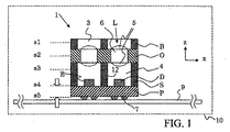
図1に示されるように、光電子モジュール1は、少なくとも1つのアクティブ光学部品と少なくとも1つのパッシブ光学部品とを含み得る。アクティブ光学部品の例としては、フォトダイオード、イメージセンサ、LED、OLED、またはレーザーチップなどの、光感知部品または発光部品が含まれる。パッシブ光学部品の例としては、レンズ、プリズム、ミラー、または光学系(たとえば、開口紋り、イメージスクリーン、または支持体などの機械要素を含み得るパッシブ光学部品の集合)などの、屈折および/または回折および/または反射によって光の方向を変える光学部品が含まれる。図2は、図1のモジュールの構成要素の様々な横概略断面図を示し、これらの横断面のおおよその位置は、図1においてs1からs5および破線によって示される。s4およびs5については、視線の方向が矢印によって示される。
Detailed Description As shown in FIG. 1, an
モジュール1は、縦方向(すなわち、図1におけるz方向)に互いに積まれた複数の構成要素(P,S,O,B)を含む。縦(z)方向に対して垂直なx−y面(図2を参照)における方向は、横方向という。
The
モジュール1は、基板Pと、分離部材Sと、光学部材Oと、バッフル部材Bとを含み、これらは互いに積まれている。基板Pは、たとえば、プリント回路板アセンブリである。PCBアセンブリのプリント回路板(PCB)は、インタポーザという。PCBの上には、光を放出するための放出部材E(たとえば、赤外光または近赤外光を放出するための発光ダイオードなどを含む光送信器ダイ)、および放出部材Eによって放出される周波数/波長(または周波数/波長の範囲)の光を検知するための検知部材D(たとえば、赤外光または近赤外光を検知するためのフォトダイオードなどを含む光受信器ダイ)が搭載される。概して、光は電磁放射をいい、たとえば、電磁スペクトルの赤外部分、可視部分、または紫外部分における電磁放射含み得る。
The
放出部材Eおよび検知部材Dの電気接触部は、はんだボール7が取り付けられるモジュール1の外側に電気的に接続される。一部の施行例は、4つの電気接触部を含み、2つが放出部材E用であり、2つが検知部材D用である。はんだボール7を設ける代わりに、一部の施行例は、後にはんだボールが設けられ得るPCB上に接続パッドを含む。したがって、モジュール1は、たとえば、表面実装技術(SMT)を使用し、他の電子部品に隣接してプリント回路基板9上に搭載され得る。プリント回路基板9は、手持ち通信装置などの電子装置10の構成要素であり得る。たとえば、装置10は、スマートフォンまたは他の携帯電話であり得る。モジュール1は、このような用途に特に適している。なぜなら、モジュール1は特に小さいサイズを有するように製造され得るためである。
The electrical contact portions of the discharge member E and the detection member D are electrically connected to the outside of the
分離部材Sは2つの開口4を有し、放出部材Eがその一方に配置され、検知部材Dが他方に配置される。この方法により、放出部材Eおよび検知部材Dは、横方向において分離部材Sによって囲まれる。開口は実質的に円形で示されるが、一部の施行例においては他の形状を有してもよい。 The separation member S has two openings 4, the discharge member E is disposed on one of them, and the detection member D is disposed on the other. By this method, the discharge member E and the detection member D are surrounded by the separation member S in the lateral direction. The openings are shown as being substantially circular, but may have other shapes in some implementations.
分離部材Sは、いくつかの役割を果たし得る。分離部材Sは、基板Pと光学部材Oとの間の(縦方向に延在する)距離が良好に規定されるように確保し得て、これにより、放出部材Eから光学部材Oを介した光路、およびモジュール1の外側から光学部材Oを介して検知部材Dへ向かう光路を良好に規定することを補助する。また、分離部材Sは、検知部材Dによって概ね検知可能な光を実質的に透過させないことにより、およびモジュール1の外側壁の部分を形成することにより、本来検知部材Dによって検知されるべきではない光から検知部材Dを保護し得る。また、分離部材Sは、検知部材Dによって概ね検知可能な光を実質的に透過させないことにより、および放出部材Eと検知部材Dとの間に壁を形成することにより、放出部材Eと検知部材Dとの間の光の相互干渉を減少させるように、検知部材Dに到達すべきでない放出部材Eから放出される光から検知部材Dを保護し得る。この方法によって、モジュール1の内側で反射した光、および放出部材Eから生じる迷光が検知部材Dに到達しないように防止され得る。一部の施行例において、分離部材Sは、たとえば、エポキシ樹脂、アクリレート、ポリウレタン、およびシリコーン材料などの硬化することが可能な(たとえば、硬化可能な)ポリマー材料である、不透明なポリマー材料からなる。分離部材は、たとえば、カーボンブラックを含有するエポキシからなり得る。
The separating member S can play several roles. The separating member S can ensure that the distance between the substrate P and the optical member O (extending in the longitudinal direction) is well defined, whereby the separating member S passes through the optical member O from the emitting member E. It assists in favorably defining the optical path and the optical path from the outside of the
最大の感度および検知範囲を実現するために、放出部材(たとえば、LED)Eと検知部材(たとえば、フォトダイオード)Dとの距離を近くすることが重要となり得る。しかしながら、内部での相互干渉によるセンサの誤反応およびダイナミックレンジの減少を回避するために、受信器の近くに位置する放出器には、分離壁またはカバーによるIR有効光学絶縁(IR-effective optical insulation)が必要である。分離部材Sは、放出部材Eと検知部材Dとを互いに分離する縦壁分割部分12を有し、内部における光の相互干渉の減少を補助し得る。
In order to achieve maximum sensitivity and sensing range, it may be important to reduce the distance between the emitting member (eg, LED) E and sensing member (eg, photodiode) D. However, in order to avoid sensor misreactions and reduced dynamic range due to internal mutual interference, emitters located near the receiver must be separated by IR-effective optical insulation by separating walls or covers. )is necessary. The separation member S has a vertical
光学部材Oは、遮断部分bと2つの透明部分tとを含み、透明部分tの一方は、放出部材Eから放出される光がモジュール1から出ることを可能とし、他方は、光がモジュール1の外側からモジュール1に入って検知部材Dに到達することを可能とする。
The optical member O includes a blocking portion b and two transparent portions t, one of the transparent portions t allowing light emitted from the emitting member E to exit the
遮断部分bは、たとえば適した(ポリマー)材料からなることにより、検知部材Dによって概ね検知可能な光を実質的に通さない。透明部分tの各々は、光をガイドするためのパッシブ光学部品L、または特定的な例として、レンズ部材Lを含む。レンズ部材Lは、たとえば、図1に示されるように、透明要素6に密着する2つのレンズ要素5を含む。透明要素6は、遮断部分bを形成する光学部材Oと同じ縦寸法を有し得て、遮断部分bを形成する光学部材Oと透明要素6とにより、(完全に近い(close-to-perfect))固体板形状が作られる。レンズ要素5(図1を参照)は、屈折および/または回折によって光の方向を変える。たとえば、レンズ要素は、(図1に示されるように)全てが概ね凸面形状からなるが、レンズ要素5の1つ以上は、たとえば全体的または部分的に凹面になるなど、異なる形状を有し得る。
The blocking portion b is made of, for example, a suitable (polymer) material, so that light that is substantially detectable by the detection member D is not substantially transmitted. Each of the transparent portions t includes a passive optical component L for guiding light or, as a specific example, a lens member L. The lens member L includes, for example, two
バッフル部材Bは、望ましくない光、特に所望の角度でモジュール1を出る光またはモジュール1に入射する光を防護し得る。バッフル部材Bは、開口として形成される、または透明な材料によって形成される、2つの別個の透明領域3を有し得る。透明領域3の外側において、バッフル部材Bは、検知部材によって概ね検知可能な光を実質的に減衰または遮断する材料からなり得る、またはこのような特性を有するコーティングが設けられ得る。しかしながら、後者の製造はより複雑であり得る。バッフル部材Bの形状、より正確には透明領域3の形状は、図1および図2に示されるものとは異なるものであり得る(たとえば、円錐状の形状または頂部の切り取られたピラミッド)。
The baffle member B may protect unwanted light, particularly light exiting the
透明領域3の横形状のみならず、透明部分tおよび開口4の横形状も円形である必要はなく、たとえば角の丸まった多角形または矩形など、他の形状を有してもよい。
Not only the horizontal shape of the
モジュール1は、パッケージ化された光電子部品である。モジュール1の縦側壁は、部品P,S,O,Bによって形成される。底壁は、基板Pによって形成され、上壁は、バッフル部材B、またはバッフル部材Bと光学部材Oとを合わせたものによって形成される。
図2に見られるように、ハウジング部品ともいう4つの部品P,S,O,Bの各々は、他のハウジング部品と実質的に同じ横形状および横寸法を有する。これにより、図3および図4を参照して以下により詳細に記載されるようなモジュール1を非常に効率的な方法で製造することが容易となる。ハウジング部品P,S,O,Bの各々は、概ねブロック形状もしくは板状の形状、またはより概略的には直方体形状を有し、(バッフル部材Bおよび分離部材Sが有するような)穴もしくは開口または(光学部材Oが有するような)突起を有し得る。
As can be seen in FIG. 2, each of the four parts P, S, O, B, also referred to as housing parts, has substantially the same lateral shape and dimensions as the other housing parts. This facilitates the manufacture of the
一部の施行例において、モジュール1は近接センサである。このようなモジュール1により、たとえば検知部材Dによって生成される光電流から判定するなどにより、対象物がモジュールから所定の距離内に位置するか否かを検知することができ、放出部材Eは、たとえば光パルスの形態で発光する。たとえば、放出部材E、光学部材O、および検知部材Dは、光学部材Oの所定の距離内または距離範囲内に位置する、光を反射することが可能な表面により、放出部材Eから放出されてこの表面で反射される十分に強度の高い光を検知部材Dが検知できるように配置され得る。これ故に、放出部材Eから放出されて、光学部材Oからさらに離れて所定の距離の外側に位置するような表面で反射される光は、検知部材Dによる十分に高い光強度の検知を引き起こさない。
In some implementations,
さらに、上述のものと同じ原理に従って設計されるが、検知部材Dに加えて、追加の光検知器などの1つ以上の追加の電子部品、または1つ以上の集積回路、または2つ以上の光源を含む、モジュールを提供することができる。 In addition, designed according to the same principles as described above, but in addition to sensing member D, one or more additional electronic components such as additional photodetectors, or one or more integrated circuits, or two or more A module including a light source can be provided.
モジュール1におけるアクティブ電子部品(図1の例における放出部材Eおよび検知部材Dなど)は、パッケージ化された電子部品またはパッケージ化されていない電子部品であり得る。基板Pとの接触には、ワイヤボンディングもしくはフリップチップ技術などの技術、または従来のスルーホール技術のような任意の他の公知の表面実装技術が使用され得る。 The active electronic components in module 1 (such as emission member E and sensing member D in the example of FIG. 1) can be packaged electronic components or unpackaged electronic components. For contact with the substrate P, techniques such as wire bonding or flip chip technology, or any other known surface mount technology such as conventional through-hole technology may be used.
図3は、図1に示されるような複数のモジュールを製造するためのウエハスタックを形成するためのウエハを示す概略断面図である。概して、ウエハは、実質的にディスク形状または板形状の部品をいい、その一方向(z方向または縦方向)への伸長は、他の2つの方向(xおよびy方向、または横方向)への伸長に対して小さい。(非ブランク(non-blank))のウエハ上において、たとえば矩形のグリッド上に、複数の同様の構造または部品が配置され得る、または設けられ得る。ウエハは、開口または穴を有し得る。一部の場合において、ウエハはその横領域の大部分に材料が無い状態となり得る。施行例に応じて、ウエハは、たとえば、半導体材料、ポリマー材料、金属とポリマーとを含む複合材料、またはポリマーとガラス材料とを含む複合材料からなり得る。特に、ウエハは、熱硬化ポリマーまたはUV硬化ポリマーなどの硬化することが可能な材料を含み得る。一部の施行例において、ウエハの直径は、5cmと40cmとの間であり、たとえば、10cmと31cmとの間であり得る。ウエハは、たとえば、2、4、6、8、または12インチの直径を有する円筒状であり得て、1インチは約2.54cmである。ウエハの厚さは、たとえば、0.2mmと10mmとの間であり得て、一部の場合においては、0.4mmと6mmとの間である。 FIG. 3 is a schematic cross-sectional view showing a wafer for forming a wafer stack for manufacturing a plurality of modules as shown in FIG. In general, a wafer refers to a substantially disk-shaped or plate-shaped part whose extension in one direction (z-direction or longitudinal direction) is in the other two directions (x- and y-direction, or lateral direction). Small to elongation. On a (non-blank) wafer, a plurality of similar structures or parts may be arranged or provided, for example on a rectangular grid. The wafer can have openings or holes. In some cases, the wafer can be free of material in most of its lateral regions. Depending on the implementation, the wafer can be composed of, for example, a semiconductor material, a polymer material, a composite material comprising a metal and a polymer, or a composite material comprising a polymer and a glass material. In particular, the wafer may include a curable material such as a thermoset polymer or a UV curable polymer. In some implementations, the diameter of the wafer is between 5 cm and 40 cm, for example, between 10 cm and 31 cm. The wafer can be, for example, cylindrical with a diameter of 2, 4, 6, 8, or 12 inches, where 1 inch is about 2.54 cm. The wafer thickness can be, for example, between 0.2 mm and 10 mm, and in some cases between 0.4 mm and 6 mm.
図3および図4は、3つのモジュール1を設けた場合を示すものであるが、一部の施行例においては、1つのウエハスタックにおいて各横方向に少なくとも10個のモジュールが設けられ得て、一部の場合において各方向に少なくとも30個または50個以上のモジュールが設けられ得る。ウエハの各々の寸法の例は、横方向に少なくとも5cmまたは10cmであり、30cmもしくは40cmまたは50cmに達し、縦方向に(基板ウエハPW上に部品が何も無い状態で測定)少なくとも0.2mmもしくは0.4mmまたは1mmであり、6mmもしくは10mmまたは20mmに達する。
3 and 4 show the case where three
一部の施行例において、図1に示されるような複数のモジュールを製造するためのウエハスタックを作成するために4つのウエハが使用され得る。図4に示されるように、スタックは、基板ウエハPWと、スペーサウエハSWと、光学ウエハOWと、バッフルウエハBWとを含む。各ウエハは、対応するモジュール1(図1および図2を参照)に含まれる多数の対応する部材を含み、これらの部材はたとえば矩形の格子上に配置され、後続の分離ステップを容易にするために互いに小さな距離が空けられている。 In some implementations, four wafers may be used to create a wafer stack for manufacturing multiple modules as shown in FIG. As shown in FIG. 4, the stack includes a substrate wafer PW, a spacer wafer SW, an optical wafer OW, and a baffle wafer BW. Each wafer includes a number of corresponding members contained in a corresponding module 1 (see FIGS. 1 and 2), which are arranged on a rectangular grid, for example, to facilitate subsequent separation steps. A small distance from each other.
基板ウエハPWは、たとえば、標準的なPCB材料からなるPCBを含むPCBアセンブリであり得て、一方側にはんだボール7が設けられ、他方側にはんだ付けされたアクティブ光学部品(たとえば、部材EおよびD)が設けられる。後者は、たとえば標準的なピックアンドプレイスマシンを使用したピックアンドプレイスによって基板ウエハPWの上に配置され得る。 The substrate wafer PW can be, for example, a PCB assembly that includes a PCB made of standard PCB material, and is provided with active optical components (eg, members E and E) provided with solder balls 7 on one side and soldered on the other side. D) is provided. The latter can be placed on the substrate wafer PW, for example by pick and place using a standard pick and place machine.
スペーサウエハSWは、基板ウエハPWおよび光学ウエハOWを実質的に互いに一定の距離を空けて維持することを補助し得る。したがって、スペーサウエハSWをウエハスタックに組み込むことにより、高い撮像性能および複雑性を可能とすることができる。スタックウエハは、その後にさいの目に切られて個別のマイクロ光学構造とされ得て、ウエハごとに複数の(たとえば、数千)の構造が得られる。 The spacer wafer SW may assist in maintaining the substrate wafer PW and the optical wafer OW at a substantially constant distance from each other. Therefore, by incorporating the spacer wafer SW into the wafer stack, high imaging performance and complexity can be achieved. The stacked wafers can then be diced into individual micro-optic structures, resulting in multiple (eg, thousands) structures per wafer.
望ましくない光の検知からの保護を最大とするために、ウエハPW,SW,OW,BWの各々は、透明部分tおよび透明領域3などの透明領域を除き、検知部材Dによって検知可能な光を実質的に通さない材料から実質的になり得る。
In order to maximize the protection from the detection of unwanted light, each of the wafers PW, SW, OW, and BW receives light that can be detected by the detection member D, except for the transparent area t and the
たとえば、一部の施行例において、スペーサウエハSWは、カーボンブラックまたは他の暗い色素を含有するUV硬化エポキシまたは熱硬化エポキシ(または他のポリマー)からなり得る。一部の施行例において、カーボンブラックはエポキシ(または他のポリマー)に埋め込まれる。エポキシ中のカーボンブラックの量は、特定の用途に依存し得て、たとえば、スペーサウエハSWの所望の光学特性または必要な光学特性に依存し得る。したがって、一部の施行例においては、光の相互干渉または検知部材Dによる他の望ましくない光の検知を減少させるために、スペーサウエハSWは、少なくとも0.7%のカーボンブラックを含有するUV硬化エポキシもしくは熱硬化エポキシからなり得る。しかしながら、一部の施行例においては、より少ない量のカーボンブラックで十分となり得る。スペーサウエハSWのためのエポキシ中の最適または所望のカーボンブラックの割合は、たとえば、壁12の横方向の厚さに応じて調整され得る。たとえば、一部の施行例において、壁の厚さは約200μmであり、エポキシ材料は、少なくとも約0.8%のカーボンブラックを含有する。800nmの波長を有する光については、前述の組成により、約0.0295/μmの吸収係数(α)が得られる。概して、厚さdを有する壁部分12については、伝達T=10−α*dとなる。したがって、前述の例において、壁部分12の伝達(T)は、0.00015%未満であり、約5.8の吸収率または光学的密度に対応する。吸収率は、材料に対する放射の量の材料を通って伝達される放射の量に対する対数比率を表わす。一部の適用例において、カーボンブラックの量は十分に高く、放出部材Eによって放出される光の波長で壁部分12を通る光の伝達(T)は0.1%以下である。同様に、一部の適用例において、カーボンブラックの量は十分に高く、放出部材Eによって放出される光の波長での壁部分12の吸収率または光学的密度は少なくとも3となる。一部の施行例において、分離部材Sは、壁12の厚さが200μmの場合は、発光素子によって放出される光の波長において少なくとも0.015/μmの吸収係数(α)を有する。
For example, in some implementations, the spacer wafer SW may consist of a UV curable epoxy or a heat curable epoxy (or other polymer) containing carbon black or other dark pigment. In some implementations, carbon black is embedded in an epoxy (or other polymer). The amount of carbon black in the epoxy can depend on the particular application, for example, depending on the desired or required optical properties of the spacer wafer SW. Accordingly, in some implementations, the spacer wafer SW is UV cured containing at least 0.7% carbon black to reduce mutual interference of light or other undesirable light detection by the sensing member D. It can consist of epoxy or thermoset epoxy. However, in some implementations, a smaller amount of carbon black may be sufficient. The optimal or desired proportion of carbon black in the epoxy for the spacer wafer SW can be adjusted depending on, for example, the lateral thickness of the
様々なポリマー材料(たとえば、エポキシ樹脂、アクリレート、ポリウレタン、またはシリコーン材料)がスペーサウエハSWの基材として使用され得て、1つ以上の色素または他の接着剤が加えられ、対象となる波長(すなわち、LEDまたは他の放出部材Eによって放出される光の波長)でのスペーサウエハの光伝達特性が減少する。スペーサウエハSWのための基材の例としては、Electronic Materials, Inc.から入手可能なEMCAST(たとえば、23xx、24xx、25xx、および2600シリーズ)、Master Bond Inc.から入手可能なMASTERBOND(商標)(たとえば、UV15-7DC、UVIODCTK)、DELO Industrial Adhesivesから入手可能なDELO-DUALBOND(商標)(たとえば、AD VE 80342)、Addison Clear Waveから入手可能なAC A1449、Epoxy Technology, Inc.から入手可能なEPOTEK OG198-54、およびLOCTITE 334、392、5091のうちの1つ以上が含まれる。前述の材料の一部は、デュアルキュア型である(すなわち、UV光および熱によって硬化させることができる)。対象となる波長においてスペーサーウエハSWの光伝達特性を減少させるために、カーボンブラックまたは他の色素が基材に加えられ得る。たとえば、カーボンブラックまたは他の色素は、放出部材Eによって放出される光の波長において壁部分12を通過する光の伝達(T)が0.1%以下となるように十分に大きな量で基礎ポリマー材料に加えられ得る。同様に、一部の適用例において、色素の量は十分に大きく、放出部材Eによって放出される光の波長において壁部分12の吸収率または光学的密度が少なくとも3となる。
Various polymeric materials (eg, epoxy resins, acrylates, polyurethanes, or silicone materials) can be used as a substrate for the spacer wafer SW and one or more dyes or other adhesives can be added to the wavelength of interest ( That is, the light transmission characteristics of the spacer wafer at the wavelength of the light emitted by the LED or other emitting member E) are reduced. Examples of substrates for spacer wafer SW include EMCAST (eg, 23xx, 24xx, 25xx, and 2600 series) available from Electronic Materials, Inc., MASTERBOND ™ (available from Master Bond Inc.) For example, UV15-7DC, UVIODCTK), DELO-DUALBOND ™ (eg AD VE 80342) available from DELO Industrial Adhesives, AC A1449 available from Addison Clear Wave, EPOTEK available from Epoxy Technology, Inc. OG198-54, and one or more of LOCTITE 334, 392, 5091 are included. Some of the aforementioned materials are of dual cure type (ie can be cured by UV light and heat). Carbon black or other dyes can be added to the substrate to reduce the light transfer properties of the spacer wafer SW at the wavelength of interest. For example, carbon black or other pigment may be a sufficiently large amount of the base polymer such that the transmission (T) of light through the
スペーサウエハSWおよびバッフルウエハBW、ならびに光学ウエハOWの少なくとも一部は、たとえば複製により作製され得る。複製は、たとえばエッチング、エンボス加工、モールド成形、または真空注入など、所与の構造またはそのネガを再現する技術をいう。複製工程の特定の例において、構造化された表面が、液体材料、粘性材料、または塑性変形可能材料にエンボス加工され、紫外放射または加熱を用いた硬化によって材料が硬化され、構造化された表面が取り除かれる。したがって、構造化された表面を有する複製物(この場合においては、ネガ複製物)が得られる。複製に適した材料は、たとえば、硬化させることができる(たとえば、硬化可能な)ポリマー材料または他の複製材料、すなわち硬化させるステップまたは凝固ステップ(たとえば、硬化ステップ)において液体、粘性、または組成変形可能な状態から個体の状態へ変化させることができる材料である。 The spacer wafer SW and the baffle wafer BW and at least a part of the optical wafer OW can be produced by, for example, replication. Duplication refers to a technique that reproduces a given structure or its negative, such as etching, embossing, molding, or vacuum injection. In a specific example of a replication process, a structured surface is embossed into a liquid material, viscous material, or plastic deformable material, and the material is cured by curing using ultraviolet radiation or heating, and the structured surface Is removed. Thus, a replica having a structured surface (in this case a negative replica) is obtained. Suitable materials for replication are, for example, polymeric materials that can be cured (eg curable) or other replication materials, ie liquid, viscous, or compositional deformation in the curing step or the solidification step (eg curing step) It is a material that can change from a possible state to an individual state.
したがって、たとえば、用途特定液体ポリマーの液滴をウエハ上に正確に投与することにより、ウエハレベルの複製工程が実施され得る。そして、モールドを用いてポリマーにエンボス加工が施され、紫外光を用いてポリマーを硬化させることによってウエハ上でポリマーが硬化する。そして、ウエハがモールドから分離される。この工程は、マイクロメートル単位の配列精度を伴ってウエハの他方側で繰り返され得る。一部の施行例において、複製材料は、引用によりここに援用される米国特許出願第7,704,418号に記載されるようにツールと基板の表面との間に収容され得る。 Thus, for example, a wafer level replication process can be performed by accurately dispensing droplets of application specific liquid polymer onto the wafer. Then, the polymer is embossed using a mold, and the polymer is cured on the wafer by curing the polymer using ultraviolet light. Then, the wafer is separated from the mold. This process can be repeated on the other side of the wafer with micrometer alignment accuracy. In some implementations, the replication material can be contained between the tool and the surface of the substrate as described in US Pat. No. 7,704,418, which is hereby incorporated by reference.
スペーサウエハSWを作製するのに適した複製技術が、たとえば、米国特許出願公開第2011/0039048号A1および米国仮出願第61/746,347号に開示されており、これら両方は引用によりここに援用される。スペーサウエハSWは、縁部における厚さが縁部まわりの表面箇所におけるスペーサウエハの厚さを超えるように作製され得る。この方法により、縁部がスペーサの平均厚さと比して上昇する。たとえば、スペーサウエハSW自体が概して100から1500ミクロン(μm)の厚さを有する場合、縁部が囲う表面に対する縁部の上昇は約1から10μmであり得る。 Suitable replication techniques for making the spacer wafer SW are disclosed, for example, in US Patent Application Publication No. 2011/0039048 A1 and US Provisional Application No. 61 / 746,347, both of which are hereby incorporated by reference. Incorporated. The spacer wafer SW can be fabricated such that the thickness at the edge exceeds the thickness of the spacer wafer at the surface location around the edge. This method raises the edge relative to the average thickness of the spacer. For example, if the spacer wafer SW itself generally has a thickness of 100 to 1500 microns (μm), the edge rise relative to the surface that the edge encloses can be about 1 to 10 μm.
一部の施行例において、ウエハレベルの硬化工程を通過する複製要素(たとえば、スペーサウエハSW、光学ウエハOW、および基板ウエハPW)は、熱的に安定し、たとえば温度が約260℃に達し得るリフロー工程などの加熱工程に耐え得る。熱的に安定した要素は、実質的にその全体的な形状を維持し、相対的に高い動作温度において分解されることはない。複製要素のこの特性は、概して「リフロー性」という。熱的に安定した要素を作製するために使用される材料は、たとえば、熱硬化性ポリマーまたは熱可塑性ポリマーを含み得る。 In some implementations, replication elements (eg, spacer wafer SW, optical wafer OW, and substrate wafer PW) that pass through a wafer level curing process are thermally stable, for example, temperatures can reach about 260 ° C. It can withstand a heating process such as a reflow process. A thermally stable element substantially maintains its overall shape and does not decompose at relatively high operating temperatures. This property of the replication element is generally referred to as “reflowability”. The material used to make the thermally stable element can include, for example, a thermosetting polymer or a thermoplastic polymer.
このような作製技術により、たとえば携帯電話または他の電子製品へのモジュールの組み込みが容易となる。なぜなら、モジュールを組み立てライン工程に直接的に組み込むことができるからである。一部の施行例において、リフロー可能要素は、−40℃と+85℃との間での1000時間の熱サイクル、および+85℃の温度および85%の相対湿度での1000時間の熱サイクルを含むGR−468CORE環境試験を満たす。 Such a fabrication technique facilitates the incorporation of the module into, for example, a mobile phone or other electronic product. This is because the module can be directly incorporated into the assembly line process. In some implementations, the reflowable element includes a 1000 hour thermal cycle between −40 ° C. and + 85 ° C. and a 1000 hour thermal cycle at a temperature of + 85 ° C. and 85% relative humidity. -468CORE environmental test is met.
たとえば、上に記載したように、スペーサウエハSWは、エポキシ樹脂および硬化剤から形成される熱硬化エポキシであり得て、一部の施行例においてはカーボンブラックも含有する。このようなエポキシ化合物の熱的安定性は、主にエポキシ樹脂の化学構造および硬化剤のタイプに依存する。たとえば、熱可塑性エポキシ化合物については、エポキシ化合物のガラス遷移温度は、約100℃から270℃の範囲内で異なり得る。 For example, as described above, the spacer wafer SW can be a thermoset epoxy formed from an epoxy resin and a curing agent, and in some implementations also contains carbon black. The thermal stability of such an epoxy compound mainly depends on the chemical structure of the epoxy resin and the type of curing agent. For example, for thermoplastic epoxy compounds, the glass transition temperature of the epoxy compound can vary within the range of about 100 ° C to 270 ° C.
また、複製要素は、熱的に安定した、紫外(UV)硬化エポキシまたは他のポリマー材料から形成され得る。一部の施行例において、複製要素は、「デュアルキュア型」の材料を用いて形成され得る。すなわち、材料は、2つの硬化法のうちいずれが採用されるかに応じて、熱(熱硬化)または紫外光(UV硬化)のいずれかを用いて硬化され得る。熱的に安定した硬化ポリマーに使用され得る材料の例としては、Electronic Materials, Inc.から入手可能なEMCAST(商標)(たとえば、23xx、24xx、25xx、および2600シリーズ)、Master Bond Inc.から入手可能なMASTERBOND(商標)エポキシ(たとえば、UV15-7DCおよびUVIODCTK)、DELO Industrial Adhesivesから入手可能なDELO-DUALBOND(商標)(たとえば、AD VE 80342)材料、Addison Clear Waveから入手可能なAC A 1449、Epoxy Technology, Inc.から入手可能なEPOTEK OG 198-54エポキシ、および/またはLOCTITE 334、392、および5091シリーズ材料のうち1つ以上が含まれる。 The replication element can also be formed from a thermally stable, ultraviolet (UV) curable epoxy or other polymeric material. In some implementations, the replication element may be formed using a “dual cure” material. That is, the material can be cured using either heat (thermal curing) or ultraviolet light (UV curing) depending on which of the two curing methods is employed. Examples of materials that can be used for thermally stable cured polymers include EMCAST ™ (eg, 23xx, 24xx, 25xx, and 2600 series) available from Electronic Materials, Inc., obtained from Master Bond Inc. Possible MASTERBOND ™ epoxies (eg UV15-7DC and UVIODCTK), DELO-DUALBOND ™ (eg AD VE 80342) material available from DELO Industrial Adhesives, AC A 1449 available from Addison Clear Wave, EPOTEK OG 198-54 epoxy available from Epoxy Technology, Inc. and / or one or more of the LOCTITE 334, 392, and 5091 series materials are included.
他の材料の例としては、機能性アミノシランとアミノプロピルメチルシロキサンのコポリマーとを定められた比率で有するエポキシが含まれる。硬化エポキシにおいてシリコン化合物を使用することにより、一部の施行例において、エポキシの熱的安定性、化学的耐性、および腐食耐性が向上し、トリメトキシ基を有するシランを使用することにより、接着特性がより良好となり得る。 Examples of other materials include epoxies having a functional aminosilane and aminopropylmethylsiloxane copolymer in defined ratios. By using silicon compounds in cured epoxies, in some implementations, the thermal stability, chemical resistance, and corrosion resistance of the epoxies are improved, and by using silanes with trimethoxy groups, adhesion properties are improved. Can be better.
代替的に、または加えて、硬化エポキシまたは他のポリマーの熱的安定性は、環状化合物を硬化剤として使用することによって向上し得る。たとえば、ビスフェノールAからなるエポキシ樹脂の熱的安定性は、とりわけ芳香族アミンおよび無水物、ノボラック、ビスマレイミド(たとえば、ジ(p−マレイミドフェニル)メタン)、ならびにイミダゾール誘導体を使用することによって向上し得る。追加の樹脂および硬化剤の組み合わせも、熱的安定性を向上させるために使用され得る。 Alternatively or additionally, the thermal stability of the cured epoxy or other polymer can be improved by using a cyclic compound as a curing agent. For example, the thermal stability of epoxy resins composed of bisphenol A is improved by using, inter alia, aromatic amines and anhydrides, novolacs, bismaleimides (eg, di (p-maleimidophenyl) methane), and imidazole derivatives. obtain. Additional resin and curing agent combinations may also be used to improve thermal stability.
レンズLのための材料も、適したリフロー可能な材料からなり得て、このリフロー可能な材料は、検知部材Dによって検知可能な光を透過する。スペーサウエハ要素と同様に、レンズLに適した材料としては、たとえば、硬化することができる(たとえば、硬化可能)ポリマー材料、または硬化する(たとえば、硬化)ステップにおいて液体、粘性、または塑性変形可能な状態から個体の状態へ変態する材料が含まれ得る。一部の施行例において、レンズ材料の硬化は、熱、UV光、または化学添加剤をポリマー材料に加えることによって実現される。スペーサウエハSW、光学ウエハOW、または基板ウエハPWを作製するために使用されるものと同じポリマー材料が、カーボンブラックを除き、レンズ材料として使用され得る。レンズを形成するために使用され得る他のポリマー材料としては、たとえば、ThreeBond Co., Ltd.から入手可能なTHREEBOND(商標)3078A、3078B、もしくは3078Cシリーズのエポキシ、DELO Industrial Adhesivesから各々が入手可能なDELO-KATIOBOND(商標)AD VE 18499エポキシおよびDELO-PHOTOBOND(商標)エポキシ(たとえば、GB368および19923シリーズ)、EPOTEK(商標)エポキシ(たとえば、90-172-4、90-174-3、100-24-3、もしくはOG142-13シリーズのエポキシ)、Kyoritsu Chemical & Co., Ltd.から入手可能なKyoritsu XLM-C5もしくはXRC 9-2シリーズのエポキシ、Micro Resist Technology GmbHから入手可能なMRT Ormocomp(商標)US-S4エポキシ、Showa Denko K.K.から入手可能なShowa Denko(商標)SAS008L-Pエポキシ、ならびに/またはWellomer Adhesive Technologyから入手可能なWELLOMER(商標)エポキシDUV 764エポキシのうちの1つ以上が含まれる。 The material for the lens L can also consist of a suitable reflowable material, which transmits light that can be detected by the detection member D. Similar to the spacer wafer element, suitable materials for the lens L include, for example, a polymer material that can be cured (eg, curable), or liquid, viscous, or plastically deformable in the curing (eg, curing) step. Materials that transform from a normal state to an individual state may be included. In some implementations, curing of the lens material is achieved by adding heat, UV light, or chemical additives to the polymer material. The same polymer material used to make the spacer wafer SW, the optical wafer OW, or the substrate wafer PW can be used as the lens material except for carbon black. Other polymeric materials that can be used to form the lens include, for example, THREEBOND ™ 3078A, 3078B, or 3078C series epoxies available from ThreeBond Co., Ltd., each from DELO Industrial Adhesives DELO-KATIOBOND ™ AD VE 18499 epoxy and DELO-PHOTOBOND ™ epoxy (eg GB368 and 19923 series), EPOTEK ™ epoxy (eg 90-172-4, 90-174-3, 100- 24-3 or OG142-13 series epoxy), Kyoritsu XLM-C5 or XRC 9-2 series epoxy available from Kyoritsu Chemical & Co., Ltd., MRT Ormocomp (trademark) available from Micro Resist Technology GmbH 1) US-S4 epoxy, Showa Denko ™ SAS008L-P epoxy available from Showa Denko KK, and / or WELLOMER ™ epoxy DUV 764 epoxy available from Wellomer Adhesive Technology Which contains more than.
光学ウエハOWについては、不透明部分(たとえば、遮断部分b)を得るために複製またはモールド成形が使用され得る。また、穿孔またはエッチングにより、透明部分が設けられる穴を設けることが可能である。続いて、このように得られた前形ウエハには、レンズ部材Lが設けられ、光学ウエハOWがもたらされる。これは、たとえばレンズ部材Lを単一の部品として形成するなど、複製によって達成され得る。しかしながら、レンズ部材Lは、透明領域3が規定される穴の中に透明要素6を含むウエハである半仕上げ部品から製造を始めることができる。これは、レンズ部材Lの各々が少なくとも1つの頂点を有し、これらの頂点が光学ウエハOWの縦断面の外側に位置する場合には特に有用となり得る。このような半仕上げ部品は、透明領域3にウエハを貫通する穴を有さず、実質的に表面の起伏を有さない、もしくは浅い表面の起伏を有する平坦なディスク状のウエハであり得る。このような表面の起伏は通常は凹面である。すなわち、起伏は、遮断部分bのようにウエハ面を超えて延在しない。
For the optical wafer OW, replication or molding can be used to obtain an opaque portion (eg, a blocking portion b). It is also possible to provide a hole in which a transparent part is provided by drilling or etching. Subsequently, the front wafer obtained in this way is provided with a lens member L, resulting in an optical wafer OW. This can be achieved by replication, for example forming the lens member L as a single part. However, the lens member L can be manufactured from a semi-finished part, which is a wafer comprising a
このような半仕上げ部品は、透明部分が設けられる穴または開口を有する平坦な前形ウエハ(通常は、1つの材料からなる)から始め、たとえば分注工程を使用して穴を透明材料で満たし、たとえばフリップチップ技術などにおけるアンダーフィル処理に使用される分注器を使用して1つずつ前形ウエハの穴を1つずつ満たす、または、たとえばスキージ処理(たとえば、スクリーン印刷から既知のもの)もしくは材料を出す複数の中空針を有する分注器を使用して一度に複数の穴を満たすことによって得られる。分注時において、ウエハはたとえばシリコーンからなる平坦な支持板の上に置かれ得る。分注された材料における気泡または空洞の形成を防止するよう注意する必要がある。なぜなら、これにより、生産されるレンズ部材Lの光学的性質が劣化し得るためである。たとえば、分注は、ウエハによって形成される縁部および下方の支持板(またはこのような縁部に近い場所)で、たとえば材料を出す中空の針をこのような縁部の近くに適切にガイドすることによって、ウエハ材料のウェッティングを開始するような方法で行うことができる。続いて、分注された材料は、たとえば熱またはUV放射によって硬化され、硬化した透明材料が得られる。 Such semi-finished parts start with a flat front wafer (usually made of one material) with holes or openings provided with transparent parts and fill the holes with transparent material, for example using a dispensing process. Fill the holes in the front wafer one by one using a dispenser used for underfill processing, for example in flip chip technology, or squeegee processing (eg known from screen printing) Alternatively, it can be obtained by filling a plurality of holes at once using a dispenser having a plurality of hollow needles for dispensing the material. During dispensing, the wafer can be placed on a flat support plate made of, for example, silicone. Care must be taken to prevent the formation of bubbles or cavities in the dispensed material. This is because the optical properties of the produced lens member L can be deteriorated. For example, dispensing can be done by guiding the hollow needles out of the material, for example, at the edges formed by the wafer and the lower support plate (or close to such edges), eg near the edges. By doing so, it can be performed in such a way as to start the wetting of the wafer material. Subsequently, the dispensed material is cured, for example by heat or UV radiation, to obtain a cured transparent material.
この方法により形成され得る凸状のメニスカスは、研磨によって平坦にされ、これにより、ウエハの厚さに調整された平行面を有する透明要素6が得られる。そして、複製により、レンズ要素5がウエハOWの一方側または両側(上側および底側)に施される。透明要素のメニスカスが凹状の場合、複製がこれらの上で行われ得て、施される複製材料の量はこれに伴って調整され得る。
The convex meniscus that can be formed by this method is flattened by polishing, whereby a
光学ウエハOWならびにスペーサウエハSWおよび/またはバッフルウエハBWの特徴および機能性を組み込んだ組み合わせ光学ウエハを設けることができる。このような組み合わせ光学ウエハの作成は、特定の前形ウエハと、これをもとに製造される特定の半仕上げ部品とによって達成され得る。このような前形ウエハおよび半仕上げ部品は、それぞれ、少なくとも1つの構造化された表面を有し、この構造化された表面は、通常はそれぞれが前形ウエハに設けられて半仕上げ部品にある透明要素の2つの表面のうち少なくとも1つを超えて縦方向に延在する突起を有する。図5において、1つの構造化された表面を有する半仕上げ部品оw′の例が概略的に示される。半仕上げ部品は、図1に示されるモジュールの製造に使用され得る。図4のウエハOWおよびSW(またはウエハOWおよびBW、またはウエハOWおよびSWおよびBW)を1つの部品として考えることにより、組み合わせ光学ウエハが図1に係るモジュールの製造のために提供される。 A combined optical wafer can be provided that incorporates the features and functionality of the optical wafer OW and spacer wafer SW and / or baffle wafer BW. The creation of such a combined optical wafer can be accomplished by a specific front wafer and a specific semi-finished part that is manufactured from it. Such a front wafer and a semi-finished part each have at least one structured surface, which is usually provided on the front wafer and is in a semi-finished part. Protrusions extending longitudinally beyond at least one of the two surfaces of the transparent element. In FIG. 5, an example of a semi-finished part оw ′ having one structured surface is schematically shown. Semi-finished parts can be used in the manufacture of the module shown in FIG. Considering wafers OW and SW (or wafers OW and BW, or wafers OW and SW and BW) of FIG. 4 as one part, a combined optical wafer is provided for the manufacture of the module according to FIG.
ウエハスタック2を形成するために、たとえば、熱硬化および/またはUV硬化エポキシ樹脂を使用して糊付けすることにより、ウエハが配列および接着される。各アクティブ光学部品(基板ウエハPW上の検知部材Dおよび放出部材Eなど)は、十分かつ正確に対応するパッシブ光学部品(光学ウエハOWのレンズ部材Lなど)と整列させる必要がある。一部の施行例において、基板ウエハPWに穴が形成され得て、穴は基板ウエハPWの厚さを貫通して延在し、圧力の蓄積を解放するためにリフロー工程時のガス抜きを提供する。穴は、穿孔またはエッチング処理により、基板ウエハPWに形成され得る。
To form the
図4は、図1に示されるような複数のモジュール1を製造するためのウエハスタック2を示す断面図である。細い破線の矩形は、たとえばダイシングソーを使用した分離が行われる場所を示す。
FIG. 4 is a cross-sectional view showing a
配列ステップの大部分がウエハレベルで行われるという事実により、相対的に簡易かつ迅速な方法で良好な配列(特に部材Lに対する部材DおよびEの配列)を実現することが可能となる。このため、全体的な製造工程が非常に速く正確となり得る。ウエハスケールの製造により、複数のモジュール1を製造するために必要な製造ステップがごく少数となる。
The fact that most of the alignment steps are performed at the wafer level makes it possible to achieve a good alignment (particularly the alignment of the members D and E with respect to the member L) in a relatively simple and rapid manner. This can make the overall manufacturing process very fast and accurate. Due to the manufacture of the wafer scale, only a few manufacturing steps are required to manufacture the plurality of
上記のように、一部の施行例において、モジュール1は近接センサモジュールである。上記の技術により、ウエハレベルの製造工程を使用して同時に複数のモジュールを作製することができる。パッケージ化されたモジュール1は、携帯電子装置、手持ち携帯電子装置、パーソナルコンピューティング装置、カメラ、オーディオもしくはビデオ再生装置、ラップトップコンピューター、または携帯情報端末などの幅広い装置に組み込むことができるとともに動作的に接続することができる。
As noted above, in some implementations,
近接センサモジュール1の特定の適用例は、携帯電話10にある(図6を参照)。たとえば、近接センサモジュール1は、ディスプレイが使用されていない時に携帯電話のディスプレイを自動的に暗くする、または非アクティブ化することによって電話の電池の寿命を長くするように、ユーザの耳または顔の横に携帯電話があることを検知するために使用され得る。図7に示されるように、携帯電話10の一部の施行例は、他の部品の中で、プロセッサ52と、メモリ64と、ディスプレイ54などの入出力装置と、通信用インターフェース66と、トランシーバ68とを含む。様々な構成要素は、様々な経路を使用して相互に接続され得て、構成部品のいくつかは、共通の主回路基板の上に、または適切な他の態様で搭載され得る。また、近接センサモジュール1は、装置10の他の構成部品に相互に接続され得て、一部の施行例においては、他の構成部品の一部とともに共通の主回路基板の上に搭載され得る。
A specific application example of the
いくつかの施行例について記載した。これに関わらず、本発明の主旨および範囲から逸脱することなく、様々な変更がなされ得ることが理解されるであろう。このため、他の施行令は、請求項の範囲内となる。 Several implementation examples were described. Nevertheless, it will be understood that various modifications can be made without departing from the spirit and scope of the invention. For this reason, other enforcement orders are within the scope of the claims.
近接センサモジュール1の特定の適用例は、携帯電話10にある(図6を参照)。たとえば、近接センサモジュール1は、ディスプレイが使用されていない時に携帯電話のディスプレイを自動的に暗くする、または非アクティブ化することによって電話の電池の寿命を長くするように、ユーザの耳または顔の横に携帯電話があることを検知するために使用され得る。図7に示されるように、携帯電話10の一部の施行例は、他の部品の中で、プロセッサ51と、メモリ64と、ディスプレイ54などの入出力装置と、通信用インターフェース66と、トランシーバ68とを含む。様々な構成要素は、様々な経路を使用して相互に接続され得て、構成部品のいくつかは、共通の主回路基板の上に、または適切な他の態様で搭載され得る。また、近接センサモジュール1は、装置10の他の構成部品に相互に接続され得て、一部の施行例においては、他の構成部品の一部とともに共通の主回路基板の上に搭載され得る。
A specific application example of the
Claims (19)
基板と、
前記基板の第1の表面上に搭載される発光素子とを備え、前記発光素子は第1の波長の光を放出するように動作可能であり、光学式近接センサモジュールはさらに、
前記基板の前記第1の表面上に搭載される光検知器を備え、光検知器は前記第1の波長の光を検知するように動作可能であり、光学式近接センサモジュールはさらに、
第1のポリマー材料から構成され、前記基板に対して実質的に平行に取り付けられる光学部材を備え、前記光学部材は、前記第1の波長の光を透過する第1および第2の透明部分を含み、前記光学部材はさらに、前記第1の波長の入射光を実質的に減衰または遮断する遮断部分を含み、前記第1の部分は前記発光素子の上方に取り付けられ、前記第2の部分は前記光検知器の上方に取り付けられ、光学式近接センサモジュールはさらに、
第2のポリマー材料から構成される分離部材を備え、前記分離部材は、前記基板と前記光学部材との間に接触して取り付けられ、前記分離部材は前記発光素子および前記光検知器を囲み、
前記第1のポリマー材料および前記第2のポリマー材料の各々は、少なくとも260℃まで熱的に安定する、光学式近接センサモジュール。 An optical proximity sensor module,
A substrate,
A light emitting device mounted on the first surface of the substrate, the light emitting device is operable to emit light of a first wavelength, and the optical proximity sensor module further comprises:
A light detector mounted on the first surface of the substrate, the light detector operable to detect light of the first wavelength, and the optical proximity sensor module further comprising:
An optical member made of a first polymer material and mounted substantially parallel to the substrate, the optical member comprising first and second transparent portions that transmit light of the first wavelength. The optical member further includes a blocking portion that substantially attenuates or blocks incident light of the first wavelength, wherein the first portion is mounted above the light emitting element, and the second portion is The optical proximity sensor module is mounted above the photodetector, and further includes
A separation member made of a second polymer material, wherein the separation member is attached in contact between the substrate and the optical member, and the separation member surrounds the light emitting element and the photodetector;
An optical proximity sensor module, wherein each of the first polymer material and the second polymer material is thermally stable to at least 260 ° C.
複数の発光素子が搭載されるとともに複数の光検知器が搭載される第1の表面を有する基板ウエハを設けるステップを備え、各発光素子は対応する1つの光検知器に隣接して取り付けられ、前記発光素子および前記光検知器は配列して前記ウエハ上に搭載され、前記発光素子は第1の波長の光を放出するように動作可能であり、前記光検知器は前記第1の波長の光を検知するように動作可能であり、方法はさらに、
少なくとも260℃まで熱的に安定する第1のポリマー材料から構成されるスペーサウエハを設けるステップを備え、前記スペーサウエハは、前記基板ウエハ上の前記発光素子および前記光検知器の配列に実質的に対応した配列の開口を有し、方法はさらに、
約260℃まで熱的に安定する第2のポリマー材料から構成される光学ウエハを設けるステップを備え、前記光学ウエハは、(1)前記第1の波長の入射光を実質的に減衰または遮断する遮断部分と、(2)前記第1の波長の光を透過する複数の第1および第2の透明部分とを含み、前記第1および第2の透明部分は、前記基板ウエハ上の前記発光素子および前記光検知器の配列に実質的に対応する配列で配置され、方法はさらに、
前記基板ウエハと、前記スペーサウエハと、前記光学ウエハとを合わせてウエハスタックに接着するステップを備え、前記ウエハスタックにおいて、前記発光素子および前記光検知器が前記基板ウエハと前記光学ウエハとの間に取り付けられるように、前記スペーサウエハは、前記基板ウエハと前記光学ウエハとの間に配置され、方法はさらに、
前記ウエハスタックを複数のモジュールに分離するステップを備え、前記複数のモジュールの各々は、前記発光素子の1つおよび前記光検知器の1つを含む、方法。 A method of making a plurality of optical proximity sensor modules, the method comprising:
Providing a substrate wafer having a first surface on which a plurality of light emitting elements are mounted and a plurality of photodetectors are mounted, each light emitting element being mounted adjacent to a corresponding one of the photodetectors; The light emitting element and the photodetector are arranged and mounted on the wafer, the light emitting element is operable to emit light of a first wavelength, and the light detector is of the first wavelength. Operable to detect light, the method further comprises:
Providing a spacer wafer comprised of a first polymer material that is thermally stable to at least 260 ° C., wherein the spacer wafer is substantially in the array of light emitting elements and photodetectors on the substrate wafer. Having a corresponding array of openings, the method further comprising:
Providing an optical wafer comprised of a second polymeric material that is thermally stable to about 260 ° C., the optical wafer comprising: (1) substantially attenuating or blocking incident light of the first wavelength. A light blocking element; and (2) a plurality of first and second transparent portions that transmit light of the first wavelength, wherein the first and second transparent portions are the light emitting elements on the substrate wafer. And an array substantially corresponding to the array of photodetectors, the method further comprising:
The substrate wafer, the spacer wafer, and the optical wafer are combined and bonded to a wafer stack, wherein the light emitting element and the light detector are disposed between the substrate wafer and the optical wafer. The spacer wafer is disposed between the substrate wafer and the optical wafer, the method further comprising:
Separating the wafer stack into a plurality of modules, each of the plurality of modules including one of the light emitting elements and one of the photodetectors.
プロセッサと、
メモリと、
ディスプレイと、
通信インターフェイスと、
トランシーバと、
光学式近接センサモジュールとを含み、光学式近接センサモジュールは、
基板と、
前記基板の第1の表面上に搭載される発光素子とを含み、前記発光素子は第1の波長の光を放出するように動作可能であり、光学式近接センサモジュールはさらに、
前記基板の前記第1の表面上に搭載される光検知器を含み、前記光検知器は前記第1の波長の光を検知するように動作可能であり、光学式近接センサモジュールはさらに、
少なくとも260℃まで熱的に安定する第1のポリマー材料から構成されて前記基板に対して実質的に平行に取り付けられる光学部材を含み、前記光学部材は、前記第1の波長の光を透過する第1および第2の透明部分を含み、前記光学部材はさらに、前記第1の波長の入射光を実質的に減衰または遮断する遮断部分を含み、前記第1の透明部分は前記発光素子の上方に取り付けられ、前記第2の透明部分は前記光検知器の上方に取り付けられ、光学近接モジュールはさらに、
少なくとも260℃まで熱的に安定する第2のポリマー材料から構成される分離部材を含み、前記分離部材は、前記基板と前記光学部材との間に接触して取り付けられ、前記分離部材は、前記発光素子および前記光検知器を囲む、移動通信装置。 A mobile communication device,
A processor;
Memory,
Display,
A communication interface;
A transceiver,
An optical proximity sensor module, and the optical proximity sensor module includes:
A substrate,
A light emitting device mounted on the first surface of the substrate, wherein the light emitting device is operable to emit light of a first wavelength, and the optical proximity sensor module further comprises:
A light detector mounted on the first surface of the substrate, the light detector operable to detect light of the first wavelength, and the optical proximity sensor module further comprising:
An optical member made of a first polymer material that is thermally stable to at least 260 ° C. and mounted substantially parallel to the substrate, the optical member transmitting light of the first wavelength The optical member further includes a blocking portion that substantially attenuates or blocks incident light of the first wavelength, and the first transparent portion is located above the light emitting element. And the second transparent portion is attached above the photodetector, and the optical proximity module further comprises:
Including a separation member composed of a second polymer material that is thermally stable to at least 260 ° C., wherein the separation member is mounted in contact between the substrate and the optical member, the separation member comprising: A mobile communication device surrounding a light emitting element and the photodetector.
Applications Claiming Priority (5)
| Application Number | Priority Date | Filing Date | Title |
|---|---|---|---|
| US201261620587P | 2012-04-05 | 2012-04-05 | |
| US61/620,587 | 2012-04-05 | ||
| US13/804,303 | 2013-03-14 | ||
| US13/804,303 US9063005B2 (en) | 2012-04-05 | 2013-03-14 | Reflowable opto-electronic module |
| PCT/SG2013/000132 WO2013151508A1 (en) | 2012-04-05 | 2013-04-03 | Reflowable opto-electronic module |
Related Child Applications (1)
| Application Number | Title | Priority Date | Filing Date |
|---|---|---|---|
| JP2017033644A Division JP6328813B2 (en) | 2012-04-05 | 2017-02-24 | Reflowable optoelectronic module |
Publications (2)
| Publication Number | Publication Date |
|---|---|
| JP2015519546A true JP2015519546A (en) | 2015-07-09 |
| JP2015519546A5 JP2015519546A5 (en) | 2016-06-02 |
Family
ID=49292701
Family Applications (2)
| Application Number | Title | Priority Date | Filing Date |
|---|---|---|---|
| JP2015504532A Pending JP2015519546A (en) | 2012-04-05 | 2013-04-03 | Reflowable optoelectronic module |
| JP2017033644A Active JP6328813B2 (en) | 2012-04-05 | 2017-02-24 | Reflowable optoelectronic module |
Family Applications After (1)
| Application Number | Title | Priority Date | Filing Date |
|---|---|---|---|
| JP2017033644A Active JP6328813B2 (en) | 2012-04-05 | 2017-02-24 | Reflowable optoelectronic module |
Country Status (8)
| Country | Link |
|---|---|
| US (2) | US9063005B2 (en) |
| EP (1) | EP2834844B1 (en) |
| JP (2) | JP2015519546A (en) |
| KR (1) | KR102125532B1 (en) |
| CN (1) | CN104247020B (en) |
| SG (1) | SG11201405658XA (en) |
| TW (2) | TWI584452B (en) |
| WO (1) | WO2013151508A1 (en) |
Families Citing this family (28)
| Publication number | Priority date | Publication date | Assignee | Title |
|---|---|---|---|---|
| TWI467777B (en) * | 2012-06-06 | 2015-01-01 | Pixart Imaging Inc | Package structure of optical apparatus |
| CN104122541B (en) * | 2013-04-28 | 2016-08-17 | 意法半导体研发(深圳)有限公司 | There is proximity detector equipment and the correlation technique of interconnection layer |
| CN104347644B (en) * | 2013-07-25 | 2018-06-19 | 意法半导体研发(深圳)有限公司 | Visual detector and correlation technique with lens subassembly |
| TW201505131A (en) * | 2013-07-25 | 2015-02-01 | Lingsen Precision Ind Ltd | Package structure of optical module |
| US9354111B2 (en) * | 2013-10-18 | 2016-05-31 | Maxim Integrated Products, Inc. | Wafer level lens in package |
| JP5907200B2 (en) * | 2014-03-18 | 2016-04-26 | セイコーエプソン株式会社 | Photodetection unit and biological information detection apparatus |
| US9711552B2 (en) * | 2014-08-19 | 2017-07-18 | Heptagon Micro Optics Pte. Ltd. | Optoelectronic modules having a silicon substrate, and fabrication methods for such modules |
| TWI684802B (en) | 2014-10-14 | 2020-02-11 | 新加坡商海特根微光學公司 | Optical element stack assemblies |
| CN105679753B (en) * | 2014-11-20 | 2018-05-08 | 日月光半导体制造股份有限公司 | Optical module, its manufacture method and electronic device |
| CN105789197B (en) * | 2014-12-25 | 2019-03-15 | 日月光半导体制造股份有限公司 | Optical module, its manufacturing method and the electronic device with optical module |
| US9752925B2 (en) * | 2015-02-13 | 2017-09-05 | Taiwan Biophotonic Corporation | Optical sensor |
| EP3104190B1 (en) * | 2015-06-08 | 2024-04-17 | ams AG | Optical sensor arrangement |
| JP6964071B2 (en) * | 2015-08-27 | 2021-11-10 | ヘプタゴン・マイクロ・オプティクス・プライベート・リミテッドHeptagon Micro Optics Pte. Ltd. | Wafer-level methods for manufacturing wafer laminates and optical assemblies |
| US10877239B2 (en) | 2015-11-12 | 2020-12-29 | Ams Sensors Singapore Pte. Ltd. | Optical element stack assemblies |
| US10551596B2 (en) | 2016-06-29 | 2020-02-04 | Ams Sensors Singapore Pte. Ltd. | Optical and optoelectronic assemblies including micro-spacers, and methods of manufacturing the same |
| US10243111B2 (en) | 2016-06-29 | 2019-03-26 | Ams Sensors Singapore Pte. Ltd. | Optoelectronic device subassemblies and methods of manufacturing the same |
| US10459189B2 (en) * | 2016-10-05 | 2019-10-29 | Omnivision Technologies, Inc. | Lens barrel, lens-barrel wafer, and associated method |
| CN106453723B (en) * | 2016-12-06 | 2022-10-21 | Oppo广东移动通信有限公司 | Sensor assembly and terminal |
| CN106847802B (en) * | 2016-12-29 | 2019-09-24 | 矽力杰半导体技术(杭州)有限公司 | Optical sensor package component and preparation method thereof and electronic equipment |
| US10461744B2 (en) | 2017-09-21 | 2019-10-29 | Google Llc | Proximity sensor connection mechanism |
| US11585901B2 (en) * | 2017-11-15 | 2023-02-21 | Veoneer Us, Llc | Scanning lidar system and method with spatial filtering for reduction of ambient light |
| US10859776B2 (en) * | 2018-04-06 | 2020-12-08 | The Regents Of The University Of California | Optical-electrical interposers |
| CN109461662B (en) * | 2018-09-28 | 2020-06-02 | 深圳赛意法微电子有限公司 | Packaging method of multi-point close-range inductor |
| CN113474154A (en) * | 2019-02-25 | 2021-10-01 | ams传感器新加坡私人有限公司 | Production of an optical diffuser element and optical diffuser element |
| WO2020207830A1 (en) * | 2019-04-08 | 2020-10-15 | Ams Ag | Optical sensor including integrated diffuser |
| CN112497884A (en) * | 2020-11-27 | 2021-03-16 | 瑞昌荣联环保科技有限公司 | Inferior gram force panel laminating machine |
| DE102020215033A1 (en) * | 2020-11-30 | 2022-06-02 | Robert Bosch Gesellschaft mit beschränkter Haftung | laser diode device |
| DE102021132724A1 (en) * | 2021-12-10 | 2023-06-15 | Valeo Schalter Und Sensoren Gmbh | OPTICAL VEHICLE ENVIRONMENT SENSOR, VEHICLE AND MANUFACTURING PROCESS |
Citations (3)
| Publication number | Priority date | Publication date | Assignee | Title |
|---|---|---|---|---|
| JP2004163116A (en) * | 2002-11-08 | 2004-06-10 | Sanyo Electric Co Ltd | Reflection type photosensor device |
| JP2010123620A (en) * | 2008-11-17 | 2010-06-03 | Stanley Electric Co Ltd | Manufacturing method of semiconductor device |
| JP2011113975A (en) * | 2009-11-23 | 2011-06-09 | Avago Technologies Ecbu Ip (Singapore) Pte Ltd | Infrared proximity sensor with improved crosstalk isolation |
Family Cites Families (21)
| Publication number | Priority date | Publication date | Assignee | Title |
|---|---|---|---|---|
| JPS61158606A (en) * | 1984-12-28 | 1986-07-18 | 株式会社小糸製作所 | Lighting apparatus |
| JPH11289105A (en) * | 1998-04-03 | 1999-10-19 | Citizen Electronics Co Ltd | Photoreflector and manufacture thereof |
| US6710346B2 (en) * | 2001-08-02 | 2004-03-23 | International Business Machines Corporation | Active infrared presence sensor |
| US20070216048A1 (en) | 2006-03-20 | 2007-09-20 | Heptagon Oy | Manufacturing optical elements |
| US20070284687A1 (en) | 2006-06-13 | 2007-12-13 | Rantala Juha T | Semiconductor optoelectronics devices |
| JP4720665B2 (en) * | 2006-07-31 | 2011-07-13 | パナソニック電工株式会社 | LED lighting fixtures |
| CH713513B1 (en) * | 2007-02-22 | 2018-08-31 | Em Microelectronic Marin Sa | Optoelectronic module with at least one photoreceptor circuit. |
| CN101953154B (en) | 2007-12-17 | 2016-09-07 | 豪威科技有限公司 | Have an integrated flash lamp can reflow camera model |
| US20090159200A1 (en) | 2007-12-19 | 2009-06-25 | Heptagon Oy | Spacer element and method for manufacturing a spacer element |
| US8092251B2 (en) * | 2007-12-29 | 2012-01-10 | Apple Inc. | Active electronic media device packaging |
| US8779361B2 (en) * | 2009-06-30 | 2014-07-15 | Avago Technologies General Ip (Singapore) Pte. Ltd. | Optical proximity sensor package with molded infrared light rejection barrier and infrared pass components |
| US8319170B2 (en) | 2009-07-10 | 2012-11-27 | Motorola Mobility Llc | Method for adapting a pulse power mode of a proximity sensor |
| US8097852B2 (en) | 2009-09-10 | 2012-01-17 | Avago Technologies Ecbu Ip (Singapore) Pte. Ltd. | Multiple transfer molded optical proximity sensor and corresponding method |
| US8716665B2 (en) | 2009-09-10 | 2014-05-06 | Avago Technologies General Ip (Singapore) Pte. Ltd. | Compact optical proximity sensor with ball grid array and windowed substrate |
| US8742350B2 (en) | 2010-06-08 | 2014-06-03 | Avago Technologies General Ip (Singapore) Pte. Ltd. | Proximity sensor |
| WO2012017267A1 (en) | 2010-08-03 | 2012-02-09 | Nokia Corporation | Optical proximity sensing |
| EP2659510B1 (en) | 2011-07-19 | 2019-01-09 | Heptagon Micro Optics Pte. Ltd. | Method for manufacturing opto-electronic modules |
| US8791489B2 (en) * | 2012-04-05 | 2014-07-29 | Heptagon Micro Optics Pte. Ltd. | Opto-electronic module |
| US8946620B2 (en) * | 2012-10-16 | 2015-02-03 | Avago Technologies General Ip (Singapore) Pte. Ltd. | Proximity sensor device with internal channeling section |
| DE102013202170B4 (en) * | 2013-02-11 | 2023-03-09 | Robert Bosch Gmbh | Optical sensor chip device and corresponding manufacturing method |
| TW201505132A (en) * | 2013-07-25 | 2015-02-01 | Lingsen Precision Ind Ltd | Package structure of optical module |
-
2013
- 2013-03-14 US US13/804,303 patent/US9063005B2/en active Active
- 2013-04-03 TW TW105119341A patent/TWI584452B/en active
- 2013-04-03 TW TW102112207A patent/TWI553840B/en active
- 2013-04-03 JP JP2015504532A patent/JP2015519546A/en active Pending
- 2013-04-03 KR KR1020147030935A patent/KR102125532B1/en active IP Right Grant
- 2013-04-03 EP EP13772963.8A patent/EP2834844B1/en active Active
- 2013-04-03 WO PCT/SG2013/000132 patent/WO2013151508A1/en active Application Filing
- 2013-04-03 SG SG11201405658XA patent/SG11201405658XA/en unknown
- 2013-04-03 CN CN201380018899.3A patent/CN104247020B/en active Active
-
2015
- 2015-05-18 US US14/715,201 patent/US9516152B2/en active Active
-
2017
- 2017-02-24 JP JP2017033644A patent/JP6328813B2/en active Active
Patent Citations (3)
| Publication number | Priority date | Publication date | Assignee | Title |
|---|---|---|---|---|
| JP2004163116A (en) * | 2002-11-08 | 2004-06-10 | Sanyo Electric Co Ltd | Reflection type photosensor device |
| JP2010123620A (en) * | 2008-11-17 | 2010-06-03 | Stanley Electric Co Ltd | Manufacturing method of semiconductor device |
| JP2011113975A (en) * | 2009-11-23 | 2011-06-09 | Avago Technologies Ecbu Ip (Singapore) Pte Ltd | Infrared proximity sensor with improved crosstalk isolation |
Also Published As
| Publication number | Publication date |
|---|---|
| JP6328813B2 (en) | 2018-05-23 |
| SG11201405658XA (en) | 2014-11-27 |
| TWI553840B (en) | 2016-10-11 |
| EP2834844B1 (en) | 2022-07-13 |
| KR102125532B1 (en) | 2020-06-24 |
| KR20150010721A (en) | 2015-01-28 |
| TW201635500A (en) | 2016-10-01 |
| US20150249734A1 (en) | 2015-09-03 |
| US9063005B2 (en) | 2015-06-23 |
| CN104247020A (en) | 2014-12-24 |
| CN104247020B (en) | 2018-04-24 |
| EP2834844A4 (en) | 2015-10-07 |
| US9516152B2 (en) | 2016-12-06 |
| TW201349466A (en) | 2013-12-01 |
| WO2013151508A1 (en) | 2013-10-10 |
| EP2834844A1 (en) | 2015-02-11 |
| US20130267273A1 (en) | 2013-10-10 |
| JP2017130668A (en) | 2017-07-27 |
| TWI584452B (en) | 2017-05-21 |
Similar Documents
| Publication | Publication Date | Title |
|---|---|---|
| JP6328813B2 (en) | Reflowable optoelectronic module | |
| JP2017152698A (en) | Optoelectronic module | |
| US11005001B2 (en) | Opto-electronic modules and methods of manufacturing the same and appliances and devices comprising the same | |
| US9746349B2 (en) | Opto-electronic module including a non-transparent separation member between a light emitting element and a light detecting element |
Legal Events
| Date | Code | Title | Description |
|---|---|---|---|
| A521 | Request for written amendment filed |
Free format text: JAPANESE INTERMEDIATE CODE: A523 Effective date: 20160401 |
|
| A621 | Written request for application examination |
Free format text: JAPANESE INTERMEDIATE CODE: A621 Effective date: 20160401 |
|
| A871 | Explanation of circumstances concerning accelerated examination |
Free format text: JAPANESE INTERMEDIATE CODE: A871 Effective date: 20160401 |
|
| A975 | Report on accelerated examination |
Free format text: JAPANESE INTERMEDIATE CODE: A971005 Effective date: 20160616 |
|
| A131 | Notification of reasons for refusal |
Free format text: JAPANESE INTERMEDIATE CODE: A131 Effective date: 20160621 |
|
| A02 | Decision of refusal |
Free format text: JAPANESE INTERMEDIATE CODE: A02 Effective date: 20161025 |
|
| A521 | Request for written amendment filed |
Free format text: JAPANESE INTERMEDIATE CODE: A523 Effective date: 20170224 |
|
| A911 | Transfer to examiner for re-examination before appeal (zenchi) |
Free format text: JAPANESE INTERMEDIATE CODE: A911 Effective date: 20170308 |
|
| A912 | Re-examination (zenchi) completed and case transferred to appeal board |
Free format text: JAPANESE INTERMEDIATE CODE: A912 Effective date: 20170407 |