JP2015516632A - Capacitive sensing device incorporating a metal strip on a transparent guard - Google Patents
Capacitive sensing device incorporating a metal strip on a transparent guard Download PDFInfo
- Publication number
- JP2015516632A JP2015516632A JP2015502238A JP2015502238A JP2015516632A JP 2015516632 A JP2015516632 A JP 2015516632A JP 2015502238 A JP2015502238 A JP 2015502238A JP 2015502238 A JP2015502238 A JP 2015502238A JP 2015516632 A JP2015516632 A JP 2015516632A
- Authority
- JP
- Japan
- Prior art keywords
- guard
- transparent
- metal strip
- area
- electrode surface
- Prior art date
- Legal status (The legal status is an assumption and is not a legal conclusion. Google has not performed a legal analysis and makes no representation as to the accuracy of the status listed.)
- Pending
Links
Images

Classifications
-
- G—PHYSICS
- G01—MEASURING; TESTING
- G01N—INVESTIGATING OR ANALYSING MATERIALS BY DETERMINING THEIR CHEMICAL OR PHYSICAL PROPERTIES
- G01N27/00—Investigating or analysing materials by the use of electric, electrochemical, or magnetic means
- G01N27/26—Investigating or analysing materials by the use of electric, electrochemical, or magnetic means by investigating electrochemical variables; by using electrolysis or electrophoresis
- G01N27/416—Systems
-
- G—PHYSICS
- G06—COMPUTING OR CALCULATING; COUNTING
- G06F—ELECTRIC DIGITAL DATA PROCESSING
- G06F3/00—Input arrangements for transferring data to be processed into a form capable of being handled by the computer; Output arrangements for transferring data from processing unit to output unit, e.g. interface arrangements
- G06F3/01—Input arrangements or combined input and output arrangements for interaction between user and computer
- G06F3/03—Arrangements for converting the position or the displacement of a member into a coded form
- G06F3/041—Digitisers, e.g. for touch screens or touch pads, characterised by the transducing means
- G06F3/044—Digitisers, e.g. for touch screens or touch pads, characterised by the transducing means by capacitive means
- G06F3/0443—Digitisers, e.g. for touch screens or touch pads, characterised by the transducing means by capacitive means using a single layer of sensing electrodes
-
- G—PHYSICS
- G06—COMPUTING OR CALCULATING; COUNTING
- G06F—ELECTRIC DIGITAL DATA PROCESSING
- G06F2203/00—Indexing scheme relating to G06F3/00 - G06F3/048
- G06F2203/041—Indexing scheme relating to G06F3/041 - G06F3/045
- G06F2203/04107—Shielding in digitiser, i.e. guard or shielding arrangements, mostly for capacitive touchscreens, e.g. driven shields, driven grounds
Landscapes
- Engineering & Computer Science (AREA)
- General Engineering & Computer Science (AREA)
- Theoretical Computer Science (AREA)
- Physics & Mathematics (AREA)
- General Physics & Mathematics (AREA)
- Chemical & Material Sciences (AREA)
- Health & Medical Sciences (AREA)
- Life Sciences & Earth Sciences (AREA)
- Human Computer Interaction (AREA)
- Chemical Kinetics & Catalysis (AREA)
- Molecular Biology (AREA)
- Electrochemistry (AREA)
- Analytical Chemistry (AREA)
- Biochemistry (AREA)
- General Health & Medical Sciences (AREA)
- Immunology (AREA)
- Pathology (AREA)
- Position Input By Displaying (AREA)
- Liquid Crystal (AREA)
- Geophysics And Detection Of Objects (AREA)
Abstract
本発明は、表示スクリーン(EC)を見るするための透明領域(SD)と、前記表示スクリーン上に配置される少なくとも2つの面へ接続する少なくとも1つの金属コネクタ(CF)が存在するアクセス領域(SND)と、を有するヒューマン−マシンインターフェースデバイス(AP)であって、それらの面が:− 前記透明領域内に存在する、透明抵抗導電性材料製の電極面(E,PT)と;− 前記透明領域内に存在し前記アクセス領域内へ延長している前記電極面用の能動ガードとして使用される、透明抵抗導電性材料製の導体面(G)と;である、前記デバイスに関するものである。本発明によるデバイスは、前記ガードの抵抗率を減少させるガードストリップ(PM)と呼ばれる少なくとも1つの金属ストリップ(PM)を含み、前記ガードストリップが:− 前記アクセス領域(SND)内に配置され;− 能動ガード(G)へ接続しており;そして、− 前記導体面(G)及び前記電極面(E,PT)が実質的に同一の電位であるように、前記電極面(E,PT)へ接続する前記金属リンク(CF)へ接続している。The present invention provides an access region (SD) for viewing a display screen (EC) and an access region (SD) in which there is at least one metal connector (CF) connected to at least two surfaces arranged on the display screen. A human-machine interface device (AP) having:-electrode surfaces (E, PT) made of transparent resistive conductive material present in the transparent region; And a conductive surface (G) made of a transparent resistive conductive material, used as an active guard for the electrode surface present in the transparent region and extending into the access region. . The device according to the invention comprises at least one metal strip (PM) called guard strip (PM) which reduces the resistivity of the guard, the guard strip being arranged in the access area (SND); Connected to an active guard (G); and-to the electrode surface (E, PT) such that the conductor surface (G) and the electrode surface (E, PT) are at substantially the same potential. It is connected to the metal link (CF) to be connected.
Description
本発明は、物体と電極面との間の容量測定用のデバイスに関するものである。前記デバイスは、特に、ヒューマン−マシンインターフェースコマンド用に使用される2次元容量式タッチサーフェス及び3次元容量性検出の一般的な分野における用途を見出すものである。 The present invention relates to a device for measuring capacitance between an object and an electrode surface. The device finds particular application in the general field of two-dimensional capacitive touch surfaces and three-dimensional capacitive detection used for human-machine interface commands.
通信及び作業用のデバイスは、例えば、パッド又はスクリーンのタッチコマンドインターフェースをますます利用するようになっている。例えば、携帯電話、スマートフォン、電子ノートブック、PC、マウス、タッチスクリーン、ワイドスクリーンなどを挙げることができる。 Communication and work devices are increasingly using, for example, a pad or screen touch command interface. For example, a mobile phone, a smart phone, an electronic notebook, a PC, a mouse, a touch screen, a wide screen, and the like can be given.
これらのインターフェースの数多くが容量性技術を利用している。タッチサーフェスは、電子的手段に連結された導電性電極を備えており、コマンドを実行するために、電極と検出すべき物体との間に生成される静電容量の変動を測定することが可能である。 Many of these interfaces utilize capacitive technology. The touch surface has conductive electrodes connected to electronic means, and can measure the capacitance variation generated between the electrodes and the object to be detected in order to execute commands It is.
現在の容量性技術は、行と列の形態での導電性電極の2つの層を最も頻繁に利用するものである。電子機器は、これらの行と列との間に存在する容量結合を測定する。指が能動面に対して非常に近い場合、指に近い容量結合が変更され、従って、電子機器は前記能動面の平面内に2次元位置(XY)を特定することができる。 Current capacitive technology makes the most frequent use of two layers of conductive electrodes in the form of rows and columns. The electronics measure the capacitive coupling that exists between these rows and columns. If the finger is very close to the active surface, the capacitive coupling close to the finger is changed, so that the electronic device can specify a two-dimensional position (XY) in the plane of the active surface.
この技術は、誘電体によって、指の位置及び存在を検出することが可能である。この技術は、一本以上の指の高感度表面のXY平面内での位置について非常に高い解像度を得るという利点を有する。しかしながら、この技術は、物体との接触を検出するのみであるか、又は、数ミリを超えない非常に近い接近での検出であるという欠点を有する。厚い手袋(スキー用グローブ、オートバイ用グローブなど)、長い爪、又はスタイラスでのタッチコマンドを実施することが困難である。容量性電極の感度の低さによって、厚い誘導体を介してコマンドを開始することが不可能である。 This technique can detect the position and presence of a finger with a dielectric. This technique has the advantage of obtaining a very high resolution for the position in the XY plane of the sensitive surface of one or more fingers. However, this technique has the disadvantage that it only detects contact with an object, or detection at very close proximity not exceeding a few millimeters. It is difficult to perform touch commands with thick gloves (ski gloves, motorcycle gloves, etc.), long nails, or a stylus. Due to the low sensitivity of capacitive electrodes, it is not possible to initiate commands through thick derivatives.
検出すべき物体と電極との間に生成される絶対静電容量の測定を可能にする最近の技術もある。この技術は、自己容量(self−capacitance)として公知の技術に類似している。例えば、仏国特許第2756048号:浮動容量測定ブリッジ、仏国特許第2893711号:浮動ブリッジによる容量測定用デバイス及び方法、又は仏国特許第2844349号:容量センサーを含む近接検出器を挙げることができる。これらの技術は、非常に高い解像度を有する物体−電極間容量の測定を得ることができ、そして、例えば、数センチ又は10センチの距離でさえ指を検出することができる。空間検出は、XYZ三次元で実施されるが、XY平面内でのタッチによっても実施される。この場合には、手袋を使用して又は厚い誘電体の任意のタイプを介して、コマンドを開始することが可能である。しかしながら、測定すべき容量値のレベルでの接触測定技術(タッチサーフェス)について新たな問題が明らかとなっている。実際に、行−列タイプの現在の容量性技術では、容量値は1つのpFのオーダーであるのに対して、電極間容量の最新技術は1つのfFのオーダーである。この理由から、浮遊容量を低減するために、ガードと呼ばれる遮蔽層を追加する必要がある。 There are also recent techniques that allow the measurement of the absolute capacitance generated between the object to be detected and the electrode. This technique is similar to the technique known as self-capacitance. Examples include French Patent No. 2756048: Floating capacitance measurement bridge, French Patent No. 2893711: Capacitance measurement device and method by floating bridge, or French Patent No. 2844349: Proximity detector including capacitance sensor. it can. These techniques can obtain measurements of object-electrode capacitance with very high resolution and can detect a finger, for example, even at a distance of a few centimeters or even 10 centimeters. Spatial detection is performed in three dimensions of XYZ, but is also performed by touching in the XY plane. In this case, it is possible to initiate the command using gloves or via any type of thick dielectric. However, new problems have become apparent with respect to contact measurement technology (touch surface) at the level of the capacitance value to be measured. In fact, in the current capacitive technology of the row-column type, the capacitance value is on the order of 1 pF, whereas the latest technology of interelectrode capacitance is on the order of 1 fF. For this reason, it is necessary to add a shielding layer called a guard in order to reduce stray capacitance.
現在のデバイスでは、電極層が透明材料製である必要があり、そして、前記電極層はデバイスの厚さを減少させるためにできるだけスクリーンの近くに導入(接地電位へ連結)される。これらは、ITO製である。従来、ITOは50Ω/□〜200Ω/□の抵抗率を有する。接地(スクリーン)に非常に近いガードの導入によって、ガードと接地との間の強い容量結合が作られる。ITO材料の高い抵抗率に関連するこの強い容量結合は、測定に重要な容量及び抵抗漏洩(直角位相)を生成する。一次等価図では、RC回路網が示される。容量結合はデバイスの機械アセンブリから並びにスクリーン及びガード面の表面から生じる。従って変化させることが困難である。 In current devices, the electrode layer needs to be made of a transparent material, and the electrode layer is introduced (coupled to ground potential) as close as possible to reduce the thickness of the device. These are made of ITO. Conventionally, ITO has a resistivity of 50Ω / □ to 200Ω / □. The introduction of a guard very close to ground (screen) creates a strong capacitive coupling between the guard and ground. This strong capacitive coupling, associated with the high resistivity of the ITO material, creates capacitance and resistance leakage (quadrature) that is important for measurement. In the primary equivalent diagram, an RC network is shown. Capacitive coupling arises from the mechanical assembly of the device and from the screen and guard surface surfaces. Therefore, it is difficult to change.
電極面と並行する検出用のガード面を開示する文献米国特許公開第2010/052700号公報が公知である。ガード面は外部ノイズを排除するために設計される。欧州特許公開第2420918号公報にも、金属ストリップによる外部ノイズの遮断面が開示されている。文献米国特許公開第2011/169783号公報には、接地に接続するガード面及び検出面を含むタッチスクリーンが開示されている。 A document US 2010/052700 that discloses a guard surface for detection parallel to an electrode surface is known. The guard surface is designed to eliminate external noise. European Patent Publication No. 2420918 also discloses an external noise blocking surface by a metal strip. Document US 2011/169783 discloses a touch screen including a guard surface and a detection surface connected to ground.
本発明の目的は、漏洩電流を制限するための新規デバイスを提案することにより、先行技術の欠点を克服することである。 The object of the present invention is to overcome the disadvantages of the prior art by proposing a new device for limiting the leakage current.
前述の目的は、特に正面図において、表示スクリーンを見るための透明領域と、前記表示スクリーンにわたり配置される少なくとも2つの面へ接続する少なくとも1つの金属リンクが存在するアクセス領域と、を有するヒューマン−マシンインターフェースデバイスであって、それらの面が:
− 前記透明領域内に存在する、抵抗導電性透明材料製の電極面と;
− 前記電極面の能動ガード又はシールドとして使用される、抵抗導電性透明材料製の導体面と、
であって、前記導体面が、前記透明領域内に存在しそして前記アクセス領域内へ延長しているものとする、前記デバイスによって達成される。
The aforementioned object is a human having a transparent area for viewing the display screen, in particular in a front view, and an access area in which there is at least one metal link connecting to at least two surfaces arranged over the display screen. Machine interface devices, whose aspects are:
-An electrode surface made of a resistive conductive transparent material present in the transparent region;
A conductor surface made of a resistive conductive transparent material used as an active guard or shield for the electrode surface;
Wherein the conductor surface is present in the transparent region and extends into the access region.
本発明によると、デバイスは、前記ガードの抵抗率を減少させるためのガードストリップと呼ばれる金属ストリップを少なくとも1つ含み、前記ガードストリップは:
− 前記金属リンク及び能動ガードへ接続し;そして
− アクセス領域内に配置される。
According to the invention, the device comprises at least one metal strip, called a guard strip, for reducing the resistivity of the guard, the guard strip comprising:
-Connected to said metal link and active guard; and-located in the access area.
前記デバイスによって、ガードは、金属ストリップへ接続され、それを十分に導電状態にし、そして、その有効性を保証する。前記ストリップが、ガード面上、特に、電極面の反対側の面上に配置されることが好ましい。前記金属ストリップの実装方法は、当業界と互換性がある。前記金属ストリップは、所望の抵抗率レベルに応じて、透明領域の周囲に、又は、1つ以上の側面上に、閉鎖フレームとして完全であることができる。 With the device, the guard is connected to the metal strip, making it fully conductive and guaranteeing its effectiveness. The strip is preferably arranged on the guard surface, in particular on the surface opposite the electrode surface. The method of mounting the metal strip is compatible with the industry. The metal strip can be complete as a closed frame around the transparent area or on one or more sides depending on the desired resistivity level.
アクセス領域が外側から見えない領域であることが好ましい。一般的に、携帯電話の製造業者は、特に、透明領域の周囲に不透明且つ非可視領域を規定する(前記透明領域下に広がっている金属接続部は外側から見えない)。 The access area is preferably an area that cannot be seen from the outside. In general, cell phone manufacturers define an opaque and invisible area, especially around the transparent area (the metal connections extending under the transparent area are not visible from the outside).
電極面及びガード面は、酸化インジウムスズ(ITO;tin−doped indium oxide)から設計されることが有利である。その他の透明材料、例えば、アルミニウムをドープした酸化亜鉛(AZO)又はスズをドープした酸化カドミニウムを使用することもできる。 The electrode surface and the guard surface are advantageously designed from indium tin oxide (ITO). Other transparent materials such as aluminum doped zinc oxide (AZO) or tin doped cadmium oxide can also be used.
本発明によると、金属リンクは、電子制御回路に由来するリボンケーブルであることができる。 According to the present invention, the metal link can be a ribbon cable derived from an electronic control circuit.
本発明の有利な特徴によると、導体面は浮動小数点技術によるガードである。 According to an advantageous feature of the invention, the conductor surface is a guard according to floating point technology.
透明領域が物体の検出用のタッチ領域であることが有利である。これによって、電極に近い容量での3次元検出が可能になる。 Advantageously, the transparent area is a touch area for object detection. This enables three-dimensional detection with a capacity close to that of the electrode.
金属ストリップは銀製であることができるが、その他の材料を使用することもできる。 The metal strip can be made of silver, but other materials can also be used.
本発明のその他の利点及び特徴は、非限定的である実施態様の詳細な説明及び添付の図面を分析することにより明らかになるであろう:
− 図1a及び1bは、本発明によるデバイスのダイアグラム図である;
− 図2は、電極及びガードの抵抗特性による容量電荷漏洩を示すダイアグラム図である;及び
− 図3a〜3fは金属ストリップの配置例を示す図である。
Other advantages and features of the present invention will become apparent by analyzing the detailed description of the non-limiting embodiments and the accompanying drawings:
-Figures la and lb are diagrammatic views of a device according to the invention;
FIG. 2 is a diagram showing capacitive charge leakage due to resistance characteristics of electrodes and guards; and FIGS. 3a to 3f show examples of arrangement of metal strips.
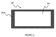
一般的に言うと、図1a及び1bは、本発明によるデバイスAPを示す。これは、「スマートフォン」タイプの電話又はタッチスクリーンを備えた電子タブレットであることができる。このデバイスAPはタッチ部である検出表面SDを含み、前記タッチ部の下には、特に、電極面(平面又は曲面)が配置される。検出表面SDは、上部から開始して、例えば:
− 外側ガラスVE;
− 破損防止フィルムFAD;
− 透明ボンドCT;及び
− 偏向板P;
− 例えば、酸化インジウムスズ(ITO)の導電性透明材料製の電極E;
− 電極用ガラス支持体S;
− 例えば、酸化インジウムスズ(ITO)の導電性透明材料製の層であるガードG;並びに、
− 外側ガラスVEの外側から目に見える必要のあるディスプレイスクリーンEC;
の透明材料製のいくつかの層を含む。
Generally speaking, FIGS. 1a and 1b show a device AP according to the invention. This can be a “smartphone” type phone or an electronic tablet with a touch screen. The device AP includes a detection surface SD that is a touch portion, and an electrode surface (a flat surface or a curved surface) is disposed below the touch portion. The detection surface SD starts from the top, for example:
-Outer glass VE;
-Anti-damage film FAD;
-Transparent bond CT; and-deflection plate P;
An electrode E made of, for example, a conductive transparent material of indium tin oxide (ITO);
A glass support S for electrodes;
A guard G, for example a layer of indium tin oxide (ITO) made of a conductive transparent material; and
A display screen EC that needs to be visible from the outside of the outer glass VE;
Including several layers of transparent material.
従って、電極及びガードは検出表面下にあり、そして、高い抵抗率導体面を有する導電性透明材料製である。 Thus, the electrodes and guard are below the detection surface and are made of a conductive transparent material having a high resistivity conductor surface.
この場合、検出表面SDを適切に包囲する非検出表面SNDも区別される。前記表面は、通常、外側から不透明であり、そして、電極を有するものではないが、金属製のストリップPT及びフレキシブルリンクCFへ接続しており、従って、ほとんど抵抗率を有さない。 In this case, a non-detection surface SND that appropriately surrounds the detection surface SD is also distinguished. The surface is usually opaque from the outside and does not have electrodes, but is connected to the metal strip PT and the flexible link CF and thus has little resistivity.
(ガードGの存在下で又は存在なしで)導電性透明材料の高い抵抗率が問題になることがある、なぜなら、デバイスへ通常接地されるスクリーンと抵抗材料との間の結合が生じるからである。電極(及びガード)は、面(電極面及び/又はガード面)全体にわたって実質的に1つの且つ同一の電位である必要がある。結合がスクリーンに存在する場合には、漏洩電流CDFが存在し、そして、前記電流は金属接続(PT,CF)から距離が遠くなるにつれてより強くなる。従って、導電性透明材料(電極及び/又はガード)とスクリーンとの間の結合は、外部ガラスの向こう側にあると仮定される対象物と電極との間で測定することが考えられる結合よりも非常に大きくなる。 The high resistivity of the conductive transparent material (in the presence or absence of the guard G) can be problematic because there is a coupling between the screen and the resistive material that is normally grounded to the device. . The electrode (and guard) needs to be at substantially one and the same potential throughout the surface (electrode surface and / or guard surface). If a bond is present on the screen, there is a leakage current CDF and the current becomes stronger as the distance from the metal connection (PT, CF) increases. Therefore, the bond between the conductive transparent material (electrode and / or guard) and the screen is more than the bond that is supposed to be measured between the object and electrode assumed to be beyond the outer glass. Become very large.
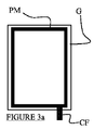
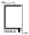
本発明によると、金属ストリップPMは、透明領域全体を包囲するフレームの形態で提供される。これは、非透明領域内のみにガードGの後面に対して押し付けられる銀ストリップである。前記ストリップPMは、ガードGのものと実質的に等しい電位を提供するフレキシブルコネクタCFと接続する。 According to the invention, the metal strip PM is provided in the form of a frame surrounding the entire transparent area. This is a silver strip that is pressed against the rear face of the guard G only in the non-transparent areas. The strip PM is connected to a flexible connector CF that provides a potential substantially equal to that of the guard G.
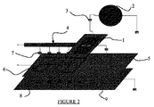
図2は、漏れ容量を表す図である。電極面1は、物体2の位置を、それらの間の容量3(Ctarget)を測定することによって検出するものとして区別することができる。物体2が接地されていることが仮定される。電極は、高い抵抗率を有するITOに基づいて設計される。後者は、一連の抵抗4によって表される。 FIG. 2 is a diagram showing the leakage capacity. The electrode surface 1 can be distinguished as detecting the position of the object 2 by measuring the capacitance 3 (Ctarget) between them. It is assumed that the object 2 is grounded. The electrodes are designed based on ITO with a high resistivity. The latter is represented by a series of resistors 4.
ガード面5もITOを含むために抵抗性である。この抵抗率は抵抗6の回路網によって表される。電荷漏洩電流7は、抵抗4と抵抗6との間に存在する。更に、漏れ容量8も、抵抗6と接地板9(通常、デバイスの表示スクリーン)との間に存在する。
The
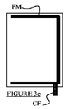
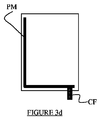
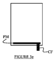
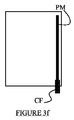
図3a〜3fは、ガードの後面、すなわち、電極の反対側の面を示す。いくつかの配列が可能である。図3aは、金属ストリップPMが閉鎖フレームである好ましい配列を示す。図3b及び3cにおいて、金属ストリップPMはC形状であり、一部が開放しているが依然としてコネクタCFと接続している。図3dにおいて、前記金属ストリップPMはL形状であり、そして、図3e及び3fにおいて、これは水平又は垂直の単一線である。 Figures 3a to 3f show the rear face of the guard, i.e. the face opposite the electrode. Several arrangements are possible. FIG. 3a shows a preferred arrangement in which the metal strip PM is a closed frame. In FIGS. 3b and 3c, the metal strip PM is C-shaped, partly open but still connected to the connector CF. In FIG. 3d, the metal strip PM is L-shaped, and in FIGS. 3e and 3f this is a horizontal or vertical single line.
勿論、本発明は以上に説明された実施例に限定されるものではなく、本発明の範囲を超えない限りで、これらの実施例に種々の調節を行うことができる。 Of course, the present invention is not limited to the embodiments described above, and various adjustments can be made to these embodiments as long as they do not exceed the scope of the present invention.
Claims (10)
− 前記透明領域内に存在する、透明抵抗導電性材料製の電極面(E,PT)と;
− 前記電極面用の能動ガード(G)として使用される、透明抵抗導電性材料製の導体面(G)と:
であって、前記導体面が、前記透明領域内に存在しそして前記アクセス領域内へ延長しているものとする、前記デバイスにおいて、
前記デバイスが、前記ガードの抵抗率を減少させるガードストリップ(PM)と呼ばれる少なくとも1つの金属ストリップ(PM)を含み、前記ガードストリップが:
− 前記能動ガード(G)へ接続しており;
− 前記導体面(G)及び前記電極面(E,PT)が実質的に1つのそして同一の電位であるように、前記電極面(E,PT)へ接続する前記金属リンク(CF)へ接続しており;そして、
− 前記アクセス領域(SND)内に配置される;
ことを特徴とする、前記デバイス。 A human-machine interface device (AP) having a transparent area (SD) for viewing a display screen (EC) and an access area (SND), the access area (SND) being arranged over the display screen There is at least one metal link (CF) connecting to at least two surfaces that are
-An electrode surface (E, PT) made of a transparent resistive conductive material present in the transparent region;
A conductor surface (G) made of a transparent resistance conductive material, used as an active guard (G) for the electrode surface;
Wherein the conductor surface is present in the transparent region and extends into the access region;
The device includes at least one metal strip (PM), called a guard strip (PM), that reduces the resistivity of the guard, the guard strip comprising:
-Connected to the active guard (G);
-Connection to the metal link (CF) connecting to the electrode surface (E, PT) such that the conductor surface (G) and the electrode surface (E, PT) are substantially at one and the same potential; And; and
-Located in the access area (SND);
Said device.
Applications Claiming Priority (3)
| Application Number | Priority Date | Filing Date | Title |
|---|---|---|---|
| FR1252619 | 2012-03-23 | ||
| FR1252619A FR2988553B1 (en) | 2012-03-23 | 2012-03-23 | CAPACITIVE DETECTION DEVICE INTEGRATING A METAL TRACK ON A TRANSPARENT GUARD. |
| PCT/EP2013/056078 WO2013139964A1 (en) | 2012-03-23 | 2013-03-22 | Capacitive sensing device incorporating a metal strip on a transparent guard |
Publications (1)
| Publication Number | Publication Date |
|---|---|
| JP2015516632A true JP2015516632A (en) | 2015-06-11 |
Family
ID=48190911
Family Applications (1)
| Application Number | Title | Priority Date | Filing Date |
|---|---|---|---|
| JP2015502238A Pending JP2015516632A (en) | 2012-03-23 | 2013-03-22 | Capacitive sensing device incorporating a metal strip on a transparent guard |
Country Status (7)
| Country | Link |
|---|---|
| US (1) | US20150068897A1 (en) |
| EP (1) | EP2828730B1 (en) |
| JP (1) | JP2015516632A (en) |
| KR (1) | KR101996703B1 (en) |
| CN (1) | CN104254825B (en) |
| FR (1) | FR2988553B1 (en) |
| WO (1) | WO2013139964A1 (en) |
Families Citing this family (19)
| Publication number | Priority date | Publication date | Assignee | Title |
|---|---|---|---|---|
| US7920129B2 (en) | 2007-01-03 | 2011-04-05 | Apple Inc. | Double-sided touch-sensitive panel with shield and drive combined layer |
| US9259904B2 (en) | 2011-10-20 | 2016-02-16 | Apple Inc. | Opaque thin film passivation |
| KR102037206B1 (en) * | 2013-04-03 | 2019-10-29 | 삼성디스플레이 주식회사 | Organic light emitting display device and method of inspecting the same |
| FR3005763B1 (en) | 2013-05-17 | 2016-10-14 | Fogale Nanotech | DEVICE AND METHOD FOR A CAPACITIVE CONTROL INTERFACE ADAPTED TO THE IMPLEMENTATION OF ELECTRODES OF HIGHLY RESISTIVE MEASUREMENTS |
| FR3008809B1 (en) * | 2013-07-18 | 2017-07-07 | Fogale Nanotech | CUSTOM ACCESSORY DEVICE FOR AN ELECTRONIC AND / OR COMPUTER APPARATUS, AND APPARATUS EQUIPPED WITH SUCH AN ACCESSORY DEVICE |
| FR3013472B1 (en) | 2013-11-19 | 2016-07-08 | Fogale Nanotech | COVERING ACCESSORY DEVICE FOR AN ELECTRONIC AND / OR COMPUTER PORTABLE APPARATUS, AND APPARATUS EQUIPPED WITH SUCH AN ACCESSORY DEVICE |
| TWI537801B (en) * | 2014-03-20 | 2016-06-11 | 原相科技股份有限公司 | Noise-cancelled capacitive touch display apparatus |
| FR3028061B1 (en) * | 2014-10-29 | 2016-12-30 | Fogale Nanotech | CAPACITIVE SENSOR DEVICE COMPRISING ADJUSTED ELECTRODES |
| FR3032287B1 (en) | 2015-02-04 | 2018-03-09 | Quickstep Technologies Llc | MULTILAYER CAPACITIVE DETECTION DEVICE, AND APPARATUS COMPRISING THE DEVICE |
| US10161814B2 (en) | 2015-05-27 | 2018-12-25 | Apple Inc. | Self-sealing sensor in an electronic device |
| US10019085B2 (en) | 2015-09-30 | 2018-07-10 | Apple Inc. | Sensor layer having a patterned compliant layer |
| CN107145253B (en) | 2016-02-19 | 2020-06-09 | 苹果公司 | Force Sensing Architecture |
| EP3516489A1 (en) * | 2016-09-23 | 2019-07-31 | Apple Inc. | Touch sensor panel with top and/or bottom shielding |
| US10372282B2 (en) | 2016-12-01 | 2019-08-06 | Apple Inc. | Capacitive coupling reduction in touch sensor panels |
| KR102750302B1 (en) | 2019-05-14 | 2025-01-08 | 삼성전자주식회사 | Display including touch sensitive circuit and method for operating thereof |
| US11531438B2 (en) | 2020-05-29 | 2022-12-20 | Apple Inc. | Differential drive and sense for touch sensor panel |
| US11789561B2 (en) | 2021-09-24 | 2023-10-17 | Apple Inc. | Architecture for differential drive and sense touch technology |
| US12260045B2 (en) | 2021-09-24 | 2025-03-25 | Apple Inc. | Architecture for differential drive and sense for touch sensor panel |
| US12197679B2 (en) | 2022-05-06 | 2025-01-14 | Apple Inc. | Touch screen shield layer with ring and tapping points |
Citations (8)
| Publication number | Priority date | Publication date | Assignee | Title |
|---|---|---|---|---|
| JPH1154984A (en) * | 1997-07-31 | 1999-02-26 | Kenwood Corp | Electromagnetic wave shield structure of electric component |
| JP2009086184A (en) * | 2007-09-28 | 2009-04-23 | Casio Comput Co Ltd | LCD with touch panel |
| US20100052700A1 (en) * | 2008-09-03 | 2010-03-04 | Rohm Co., Ltd. | Capacitive sensor |
| JP2010205220A (en) * | 2009-03-06 | 2010-09-16 | Epson Imaging Devices Corp | Touch panel |
| WO2011005977A2 (en) * | 2009-07-10 | 2011-01-13 | Apple Inc. | Touch and hover sensing |
| WO2011015794A1 (en) * | 2009-08-07 | 2011-02-10 | Nanotec Solution | Device and method for control interface sensitive to a movement of a body or of an object and control equipment integrating this device |
| US20110063247A1 (en) * | 2008-01-29 | 2011-03-17 | Dongjin Min | Touch sensing apparatus with parasitic capacitance prevention structure |
| US20120044662A1 (en) * | 2010-08-19 | 2012-02-23 | Jong-Hyuk Kim | Display device having touch panel |
Family Cites Families (10)
| Publication number | Priority date | Publication date | Assignee | Title |
|---|---|---|---|---|
| US5574262A (en) * | 1994-10-04 | 1996-11-12 | At&T Global Information Solutions Company | Noise cancellation for non-ideal electrostatic shielding |
| FR2756048B1 (en) | 1996-11-15 | 1999-02-12 | Nanotec Ingenierie | FLOATING CAPACITIVE MEASUREMENT BRIDGE AND ASSOCIATED MULTI-CAPACITIVE MEASUREMENT SYSTEM |
| US6847354B2 (en) * | 2000-03-23 | 2005-01-25 | The United States Of America As Represented By The Administrator Of The National Aeronautics And Space Administration | Three dimensional interactive display |
| FR2844349B1 (en) | 2002-09-06 | 2005-06-24 | Nanotec Solution | CAPACITIVE SENSOR PROXIMITY DETECTOR |
| FR2893711B1 (en) | 2005-11-24 | 2008-01-25 | Nanotec Solution Soc Civ Ile | DEVICE AND METHOD FOR CAPACITIVE MEASUREMENT BY FLOATING BRIDGE |
| JP5033078B2 (en) * | 2008-08-06 | 2012-09-26 | 株式会社ジャパンディスプレイイースト | Display device |
| FR2949008B1 (en) * | 2009-08-07 | 2011-09-16 | Nanotec Solution | CAPACITIVE DETECTION DEVICE WITH FUNCTION INTEGRATION. |
| TW201124766A (en) * | 2010-01-08 | 2011-07-16 | Wintek Corp | Display device with touch panel |
| KR101481674B1 (en) * | 2010-08-19 | 2015-01-14 | 엘지디스플레이 주식회사 | Display device having touch panel |
| US8698769B2 (en) * | 2011-08-01 | 2014-04-15 | Sharp Kabushiki Kaisha | Dual mode capacitive touch panel |
-
2012
- 2012-03-23 FR FR1252619A patent/FR2988553B1/en not_active Expired - Fee Related
-
2013
- 2013-03-22 WO PCT/EP2013/056078 patent/WO2013139964A1/en not_active Ceased
- 2013-03-22 CN CN201380016104.5A patent/CN104254825B/en not_active Expired - Fee Related
- 2013-03-22 JP JP2015502238A patent/JP2015516632A/en active Pending
- 2013-03-22 US US14/387,024 patent/US20150068897A1/en not_active Abandoned
- 2013-03-22 EP EP13719028.6A patent/EP2828730B1/en active Active
- 2013-03-22 KR KR1020147029118A patent/KR101996703B1/en not_active Expired - Fee Related
Patent Citations (9)
| Publication number | Priority date | Publication date | Assignee | Title |
|---|---|---|---|---|
| JPH1154984A (en) * | 1997-07-31 | 1999-02-26 | Kenwood Corp | Electromagnetic wave shield structure of electric component |
| JP2009086184A (en) * | 2007-09-28 | 2009-04-23 | Casio Comput Co Ltd | LCD with touch panel |
| US20110063247A1 (en) * | 2008-01-29 | 2011-03-17 | Dongjin Min | Touch sensing apparatus with parasitic capacitance prevention structure |
| US20100052700A1 (en) * | 2008-09-03 | 2010-03-04 | Rohm Co., Ltd. | Capacitive sensor |
| JP2010061405A (en) * | 2008-09-03 | 2010-03-18 | Rohm Co Ltd | Capacitance sensor, detection circuit thereof, input device, and control method of capacity sensor |
| JP2010205220A (en) * | 2009-03-06 | 2010-09-16 | Epson Imaging Devices Corp | Touch panel |
| WO2011005977A2 (en) * | 2009-07-10 | 2011-01-13 | Apple Inc. | Touch and hover sensing |
| WO2011015794A1 (en) * | 2009-08-07 | 2011-02-10 | Nanotec Solution | Device and method for control interface sensitive to a movement of a body or of an object and control equipment integrating this device |
| US20120044662A1 (en) * | 2010-08-19 | 2012-02-23 | Jong-Hyuk Kim | Display device having touch panel |
Also Published As
| Publication number | Publication date |
|---|---|
| EP2828730A1 (en) | 2015-01-28 |
| FR2988553B1 (en) | 2015-03-27 |
| WO2013139964A1 (en) | 2013-09-26 |
| EP2828730B1 (en) | 2019-11-06 |
| KR101996703B1 (en) | 2019-07-04 |
| KR20140147106A (en) | 2014-12-29 |
| FR2988553A1 (en) | 2013-09-27 |
| US20150068897A1 (en) | 2015-03-12 |
| CN104254825B (en) | 2018-01-30 |
| CN104254825A (en) | 2014-12-31 |
Similar Documents
| Publication | Publication Date | Title |
|---|---|---|
| KR101996703B1 (en) | Capacitive sensing device incorporating a metal strip on a transparent guard | |
| CN104321726B (en) | Device for capacitive detection using an arrangement of coupling tracks and method for implementing such a device | |
| CN105183257B (en) | Touch screen and pressure touch detection method thereof | |
| CN105224126B (en) | Touch screen and pressure touch detection method therefor | |
| KR101076234B1 (en) | Touch screen input device | |
| TWI467450B (en) | Compensation for capacitance change in touch sensing device | |
| US20170228065A1 (en) | Force-touch sensor with multilayered electrodes | |
| JP6369805B2 (en) | Touch sensor device, electronic device, and touch gesture detection program | |
| KR20180018479A (en) | A touch sensor, a touch detection device and a detection method, and a touch device | |
| CN105117080A (en) | Touch apparatus integrating pressure-sensing function | |
| KR20120139518A (en) | Hybrid touch panel for sensing capacitance and pressure | |
| KR20140066528A (en) | Touch panel and method for manufacturing the same | |
| CN204926044U (en) | Contact screen | |
| CN204904244U (en) | Contact screen | |
| US10139439B2 (en) | Method of capacitive measurement between an object and an electrode plane by partial synchronous demodulation | |
| TWM359724U (en) | Display device using touch panel | |
| JP7178972B2 (en) | Touch panel and display device | |
| KR20150081574A (en) | A touchscreen panel with high sensitivity | |
| KR101183060B1 (en) | A touch panel and its manufacturing method with equipped a ito of a resistive components of different two or more | |
| WO2015107516A1 (en) | Transparent proximity sensor |
Legal Events
| Date | Code | Title | Description |
|---|---|---|---|
| A621 | Written request for application examination |
Free format text: JAPANESE INTERMEDIATE CODE: A621 Effective date: 20160322 |
|
| A711 | Notification of change in applicant |
Free format text: JAPANESE INTERMEDIATE CODE: A711 Effective date: 20160322 |
|
| A521 | Request for written amendment filed |
Free format text: JAPANESE INTERMEDIATE CODE: A821 Effective date: 20160322 |
|
| A977 | Report on retrieval |
Free format text: JAPANESE INTERMEDIATE CODE: A971007 Effective date: 20170127 |
|
| A131 | Notification of reasons for refusal |
Free format text: JAPANESE INTERMEDIATE CODE: A131 Effective date: 20170306 |
|
| A601 | Written request for extension of time |
Free format text: JAPANESE INTERMEDIATE CODE: A601 Effective date: 20170602 |
|
| A601 | Written request for extension of time |
Free format text: JAPANESE INTERMEDIATE CODE: A601 Effective date: 20170807 |
|
| A521 | Request for written amendment filed |
Free format text: JAPANESE INTERMEDIATE CODE: A523 Effective date: 20170901 |
|
| A131 | Notification of reasons for refusal |
Free format text: JAPANESE INTERMEDIATE CODE: A131 Effective date: 20180115 |
|
| A601 | Written request for extension of time |
Free format text: JAPANESE INTERMEDIATE CODE: A601 Effective date: 20180412 |
|
| A601 | Written request for extension of time |
Free format text: JAPANESE INTERMEDIATE CODE: A601 Effective date: 20180614 |
|
| A521 | Request for written amendment filed |
Free format text: JAPANESE INTERMEDIATE CODE: A523 Effective date: 20180713 |
|
| A02 | Decision of refusal |
Free format text: JAPANESE INTERMEDIATE CODE: A02 Effective date: 20180910 |
|
| A521 | Request for written amendment filed |
Free format text: JAPANESE INTERMEDIATE CODE: A523 Effective date: 20190110 |
|
| C60 | Trial request (containing other claim documents, opposition documents) |
Free format text: JAPANESE INTERMEDIATE CODE: C60 Effective date: 20190110 |
|
| C11 | Written invitation by the commissioner to file amendments |
Free format text: JAPANESE INTERMEDIATE CODE: C11 Effective date: 20190121 |
|
| A911 | Transfer to examiner for re-examination before appeal (zenchi) |
Free format text: JAPANESE INTERMEDIATE CODE: A911 Effective date: 20190220 |
|
| C21 | Notice of transfer of a case for reconsideration by examiners before appeal proceedings |
Free format text: JAPANESE INTERMEDIATE CODE: C21 Effective date: 20190225 |
|
| A131 | Notification of reasons for refusal |
Free format text: JAPANESE INTERMEDIATE CODE: A131 Effective date: 20190422 |
|
| A601 | Written request for extension of time |
Free format text: JAPANESE INTERMEDIATE CODE: A601 Effective date: 20190722 |
|
| A601 | Written request for extension of time |
Free format text: JAPANESE INTERMEDIATE CODE: A601 Effective date: 20190920 |
|
| A912 | Re-examination (zenchi) completed and case transferred to appeal board |
Free format text: JAPANESE INTERMEDIATE CODE: A912 Effective date: 20200207 |
|
| C211 | Notice of termination of reconsideration by examiners before appeal proceedings |
Free format text: JAPANESE INTERMEDIATE CODE: C211 Effective date: 20200217 |
|
| C22 | Notice of designation (change) of administrative judge |
Free format text: JAPANESE INTERMEDIATE CODE: C22 Effective date: 20200316 |
|
| C22 | Notice of designation (change) of administrative judge |
Free format text: JAPANESE INTERMEDIATE CODE: C22 Effective date: 20200413 |
|
| C23 | Notice of termination of proceedings |
Free format text: JAPANESE INTERMEDIATE CODE: C23 Effective date: 20200803 |
|
| C03 | Trial/appeal decision taken |
Free format text: JAPANESE INTERMEDIATE CODE: C03 Effective date: 20200910 |
|
| C30A | Notification sent |
Free format text: JAPANESE INTERMEDIATE CODE: C3012 Effective date: 20200910 |