JP2015509668A - Miniaturized solid state laser oscillation device, system, and method - Google Patents
Miniaturized solid state laser oscillation device, system, and method Download PDFInfo
- Publication number
- JP2015509668A JP2015509668A JP2014560914A JP2014560914A JP2015509668A JP 2015509668 A JP2015509668 A JP 2015509668A JP 2014560914 A JP2014560914 A JP 2014560914A JP 2014560914 A JP2014560914 A JP 2014560914A JP 2015509668 A JP2015509668 A JP 2015509668A
- Authority
- JP
- Japan
- Prior art keywords
- tube
- mco
- state laser
- oscillator
- microchip
- Prior art date
- Legal status (The legal status is an assumption and is not a legal conclusion. Google has not performed a legal analysis and makes no representation as to the accuracy of the status listed.)
- Granted
Links
Images


Classifications
-
- H—ELECTRICITY
- H01—ELECTRIC ELEMENTS
- H01S—DEVICES USING THE PROCESS OF LIGHT AMPLIFICATION BY STIMULATED EMISSION OF RADIATION [LASER] TO AMPLIFY OR GENERATE LIGHT; DEVICES USING STIMULATED EMISSION OF ELECTROMAGNETIC RADIATION IN WAVE RANGES OTHER THAN OPTICAL
- H01S3/00—Lasers, i.e. devices using stimulated emission of electromagnetic radiation in the infrared, visible or ultraviolet wave range
- H01S3/05—Construction or shape of optical resonators; Accommodation of active medium therein; Shape of active medium
- H01S3/06—Construction or shape of active medium
- H01S3/0627—Construction or shape of active medium the resonator being monolithic, e.g. microlaser
-
- H—ELECTRICITY
- H01—ELECTRIC ELEMENTS
- H01S—DEVICES USING THE PROCESS OF LIGHT AMPLIFICATION BY STIMULATED EMISSION OF RADIATION [LASER] TO AMPLIFY OR GENERATE LIGHT; DEVICES USING STIMULATED EMISSION OF ELECTROMAGNETIC RADIATION IN WAVE RANGES OTHER THAN OPTICAL
- H01S3/00—Lasers, i.e. devices using stimulated emission of electromagnetic radiation in the infrared, visible or ultraviolet wave range
- H01S3/02—Constructional details
- H01S3/025—Constructional details of solid state lasers, e.g. housings or mountings
-
- H—ELECTRICITY
- H01—ELECTRIC ELEMENTS
- H01S—DEVICES USING THE PROCESS OF LIGHT AMPLIFICATION BY STIMULATED EMISSION OF RADIATION [LASER] TO AMPLIFY OR GENERATE LIGHT; DEVICES USING STIMULATED EMISSION OF ELECTROMAGNETIC RADIATION IN WAVE RANGES OTHER THAN OPTICAL
- H01S3/00—Lasers, i.e. devices using stimulated emission of electromagnetic radiation in the infrared, visible or ultraviolet wave range
- H01S3/02—Constructional details
- H01S3/04—Arrangements for thermal management
- H01S3/0405—Conductive cooling, e.g. by heat sinks or thermo-electric elements
-
- H—ELECTRICITY
- H01—ELECTRIC ELEMENTS
- H01S—DEVICES USING THE PROCESS OF LIGHT AMPLIFICATION BY STIMULATED EMISSION OF RADIATION [LASER] TO AMPLIFY OR GENERATE LIGHT; DEVICES USING STIMULATED EMISSION OF ELECTROMAGNETIC RADIATION IN WAVE RANGES OTHER THAN OPTICAL
- H01S3/00—Lasers, i.e. devices using stimulated emission of electromagnetic radiation in the infrared, visible or ultraviolet wave range
- H01S3/05—Construction or shape of optical resonators; Accommodation of active medium therein; Shape of active medium
- H01S3/08—Construction or shape of optical resonators or components thereof
- H01S3/08004—Construction or shape of optical resonators or components thereof incorporating a dispersive element, e.g. a prism for wavelength selection
- H01S3/08009—Construction or shape of optical resonators or components thereof incorporating a dispersive element, e.g. a prism for wavelength selection using a diffraction grating
-
- H—ELECTRICITY
- H01—ELECTRIC ELEMENTS
- H01S—DEVICES USING THE PROCESS OF LIGHT AMPLIFICATION BY STIMULATED EMISSION OF RADIATION [LASER] TO AMPLIFY OR GENERATE LIGHT; DEVICES USING STIMULATED EMISSION OF ELECTROMAGNETIC RADIATION IN WAVE RANGES OTHER THAN OPTICAL
- H01S3/00—Lasers, i.e. devices using stimulated emission of electromagnetic radiation in the infrared, visible or ultraviolet wave range
- H01S3/05—Construction or shape of optical resonators; Accommodation of active medium therein; Shape of active medium
- H01S3/08—Construction or shape of optical resonators or components thereof
- H01S3/086—One or more reflectors having variable properties or positions for initial adjustment of the resonator
-
- H—ELECTRICITY
- H01—ELECTRIC ELEMENTS
- H01S—DEVICES USING THE PROCESS OF LIGHT AMPLIFICATION BY STIMULATED EMISSION OF RADIATION [LASER] TO AMPLIFY OR GENERATE LIGHT; DEVICES USING STIMULATED EMISSION OF ELECTROMAGNETIC RADIATION IN WAVE RANGES OTHER THAN OPTICAL
- H01S3/00—Lasers, i.e. devices using stimulated emission of electromagnetic radiation in the infrared, visible or ultraviolet wave range
- H01S3/02—Constructional details
- H01S3/04—Arrangements for thermal management
- H01S3/042—Arrangements for thermal management for solid state lasers
-
- H—ELECTRICITY
- H01—ELECTRIC ELEMENTS
- H01S—DEVICES USING THE PROCESS OF LIGHT AMPLIFICATION BY STIMULATED EMISSION OF RADIATION [LASER] TO AMPLIFY OR GENERATE LIGHT; DEVICES USING STIMULATED EMISSION OF ELECTROMAGNETIC RADIATION IN WAVE RANGES OTHER THAN OPTICAL
- H01S3/00—Lasers, i.e. devices using stimulated emission of electromagnetic radiation in the infrared, visible or ultraviolet wave range
- H01S3/05—Construction or shape of optical resonators; Accommodation of active medium therein; Shape of active medium
- H01S3/06—Construction or shape of active medium
- H01S3/0602—Crystal lasers or glass lasers
- H01S3/061—Crystal lasers or glass lasers with elliptical or circular cross-section and elongated shape, e.g. rod
-
- H—ELECTRICITY
- H01—ELECTRIC ELEMENTS
- H01S—DEVICES USING THE PROCESS OF LIGHT AMPLIFICATION BY STIMULATED EMISSION OF RADIATION [LASER] TO AMPLIFY OR GENERATE LIGHT; DEVICES USING STIMULATED EMISSION OF ELECTROMAGNETIC RADIATION IN WAVE RANGES OTHER THAN OPTICAL
- H01S3/00—Lasers, i.e. devices using stimulated emission of electromagnetic radiation in the infrared, visible or ultraviolet wave range
- H01S3/05—Construction or shape of optical resonators; Accommodation of active medium therein; Shape of active medium
- H01S3/08—Construction or shape of optical resonators or components thereof
- H01S3/081—Construction or shape of optical resonators or components thereof comprising three or more reflectors
- H01S3/0811—Construction or shape of optical resonators or components thereof comprising three or more reflectors incorporating a dispersive element, e.g. a prism for wavelength selection
- H01S3/0812—Construction or shape of optical resonators or components thereof comprising three or more reflectors incorporating a dispersive element, e.g. a prism for wavelength selection using a diffraction grating
-
- H—ELECTRICITY
- H01—ELECTRIC ELEMENTS
- H01S—DEVICES USING THE PROCESS OF LIGHT AMPLIFICATION BY STIMULATED EMISSION OF RADIATION [LASER] TO AMPLIFY OR GENERATE LIGHT; DEVICES USING STIMULATED EMISSION OF ELECTROMAGNETIC RADIATION IN WAVE RANGES OTHER THAN OPTICAL
- H01S3/00—Lasers, i.e. devices using stimulated emission of electromagnetic radiation in the infrared, visible or ultraviolet wave range
- H01S3/09—Processes or apparatus for excitation, e.g. pumping
- H01S3/091—Processes or apparatus for excitation, e.g. pumping using optical pumping
- H01S3/094—Processes or apparatus for excitation, e.g. pumping using optical pumping by coherent light
- H01S3/094049—Guiding of the pump light
- H01S3/094053—Fibre coupled pump, e.g. delivering pump light using a fibre or a fibre bundle
-
- H—ELECTRICITY
- H01—ELECTRIC ELEMENTS
- H01S—DEVICES USING THE PROCESS OF LIGHT AMPLIFICATION BY STIMULATED EMISSION OF RADIATION [LASER] TO AMPLIFY OR GENERATE LIGHT; DEVICES USING STIMULATED EMISSION OF ELECTROMAGNETIC RADIATION IN WAVE RANGES OTHER THAN OPTICAL
- H01S3/00—Lasers, i.e. devices using stimulated emission of electromagnetic radiation in the infrared, visible or ultraviolet wave range
- H01S3/09—Processes or apparatus for excitation, e.g. pumping
- H01S3/091—Processes or apparatus for excitation, e.g. pumping using optical pumping
- H01S3/094—Processes or apparatus for excitation, e.g. pumping using optical pumping by coherent light
- H01S3/0941—Processes or apparatus for excitation, e.g. pumping using optical pumping by coherent light of a laser diode
- H01S3/09415—Processes or apparatus for excitation, e.g. pumping using optical pumping by coherent light of a laser diode the pumping beam being parallel to the lasing mode of the pumped medium, e.g. end-pumping
-
- H—ELECTRICITY
- H01—ELECTRIC ELEMENTS
- H01S—DEVICES USING THE PROCESS OF LIGHT AMPLIFICATION BY STIMULATED EMISSION OF RADIATION [LASER] TO AMPLIFY OR GENERATE LIGHT; DEVICES USING STIMULATED EMISSION OF ELECTROMAGNETIC RADIATION IN WAVE RANGES OTHER THAN OPTICAL
- H01S3/00—Lasers, i.e. devices using stimulated emission of electromagnetic radiation in the infrared, visible or ultraviolet wave range
- H01S3/10—Controlling the intensity, frequency, phase, polarisation or direction of the emitted radiation, e.g. switching, gating, modulating or demodulating
- H01S3/106—Controlling the intensity, frequency, phase, polarisation or direction of the emitted radiation, e.g. switching, gating, modulating or demodulating by controlling devices placed within the cavity
- H01S3/1061—Controlling the intensity, frequency, phase, polarisation or direction of the emitted radiation, e.g. switching, gating, modulating or demodulating by controlling devices placed within the cavity using a variable absorption device
-
- H—ELECTRICITY
- H01—ELECTRIC ELEMENTS
- H01S—DEVICES USING THE PROCESS OF LIGHT AMPLIFICATION BY STIMULATED EMISSION OF RADIATION [LASER] TO AMPLIFY OR GENERATE LIGHT; DEVICES USING STIMULATED EMISSION OF ELECTROMAGNETIC RADIATION IN WAVE RANGES OTHER THAN OPTICAL
- H01S3/00—Lasers, i.e. devices using stimulated emission of electromagnetic radiation in the infrared, visible or ultraviolet wave range
- H01S3/10—Controlling the intensity, frequency, phase, polarisation or direction of the emitted radiation, e.g. switching, gating, modulating or demodulating
- H01S3/11—Mode locking; Q-switching; Other giant-pulse techniques, e.g. cavity dumping
- H01S3/1123—Q-switching
- H01S3/113—Q-switching using intracavity saturable absorbers
-
- H—ELECTRICITY
- H01—ELECTRIC ELEMENTS
- H01S—DEVICES USING THE PROCESS OF LIGHT AMPLIFICATION BY STIMULATED EMISSION OF RADIATION [LASER] TO AMPLIFY OR GENERATE LIGHT; DEVICES USING STIMULATED EMISSION OF ELECTROMAGNETIC RADIATION IN WAVE RANGES OTHER THAN OPTICAL
- H01S3/00—Lasers, i.e. devices using stimulated emission of electromagnetic radiation in the infrared, visible or ultraviolet wave range
- H01S3/14—Lasers, i.e. devices using stimulated emission of electromagnetic radiation in the infrared, visible or ultraviolet wave range characterised by the material used as the active medium
- H01S3/16—Solid materials
- H01S3/163—Solid materials characterised by a crystal matrix
- H01S3/164—Solid materials characterised by a crystal matrix garnet
- H01S3/1643—YAG
Abstract
固体レーザ発振装置(100,200,300)が、第1の管(104,204,304)に取り付けられたマイクロチップ発振器(MCO)(102,202,302)と、第2の管(108,208,308)に取り付けられた体積ブラッグ格子(VBG)プレート(106,206,306)とを有する。第2の管は、スリップフィットで第1の管に入れ子式に結合されるように構成されており、それによって、体積ブラッグ格子(VBG)プレートは、マイクロチップ発振器(MCO)と同心状に整列されるとともにマイクロチップ発振器(MCO)から特定の距離に位置決めされる。A solid-state laser oscillator (100, 200, 300) includes a microchip oscillator (MCO) (102, 202, 302) attached to a first tube (104, 204, 304), and a second tube (108, 208, 308) and a volume Bragg grating (VBG) plate (106, 206, 306). The second tube is configured to be slip-fit and telescoped into the first tube so that the volume Bragg grating (VBG) plate is concentrically aligned with the microchip oscillator (MCO) And positioned at a specific distance from the microchip oscillator (MCO).
Description
本開示は、概して、光学及び電気光学の小型化装置を対象としており、より具体的には、固体レーザ発振装置、及び関連するシステム及びパッケージ方法を対象とする。 The present disclosure is generally directed to optical and electro-optic miniaturization devices, and more specifically to solid state laser oscillation devices and related systems and packaging methods.
放射線(レーザ)装置の誘導放出による光増幅は、光増幅を用いて光の狭ビームを発生させる。レーザからの発光は、シングルモード又はマルチモード発振のいずれかとして特徴付けることができる。シングルモード発振は、概して、1つのみ又は比較的少数の主波長を有するレーザによって生成される光を指す。一方、マルチモード発光は、概して、複数の主波長を有するレーザによって生成される光を指す。シングルモード発振は、大抵の場合に、通信に使用される場合に低減したノイズによって、及び主波長の動作で動作するように設計された簡略化された光学系によって、マルチモード発振に対して有利である。 Light amplification by stimulated emission of a radiation (laser) device generates a narrow beam of light using light amplification. The emission from the laser can be characterized as either single mode or multimode oscillation. Single mode oscillation generally refers to light generated by a laser having only one or a relatively small number of dominant wavelengths. On the other hand, multimode emission generally refers to light generated by a laser having multiple dominant wavelengths. Single mode oscillation is advantageous over multimode oscillation in most cases by reduced noise when used in communications and by simplified optics designed to operate at dominant wavelength operation. It is.
ダイオードで励起された固体レーザ技術における最近の進歩によって、各種レーザ近接センサ及びヒューズ、空間通信システム、固体レーザ送信機、及び他の多くのレーザシステムにおいて主要部品として大抵の場合に使用されるマイクロチップ発振レーザ(MCO)等のレーザ装置の開発が容易になった。ダイオード励起型マイクロチップレーザは、比較的広範な周波数範囲に亘ってその向上したシングルモードの性能によって、これらの用途において魅力的であるように思われる。これらのダイオード励起型マイクロチップレーザは、1つ又は比較的少数のモードが機能的な発振モードになる場合のみに広く分離される縦モードを示す。他の全ての要件に加えて、マイクロチップベースの発振器及びそのレーザ送信機は、正確で信頼性の高いシングルモード動作を提供する必要がある。適切なパッケージ手法は、シングルモード短パルス動作及びほぼ熱的に独立したレーザ発振のためのいくつかの重要な条件を容易にする必要がある。最も重要なものは、マルチモード及び/又は混合モード動作を除外する能力である。レーザ共振器内の温度上昇とマイクロチップレーザにおける熱ストレスとが、大抵の場合に、マルチモード及び/又は混合モード動作に影響を与えている。これらのシングルモード動作のいくつかでは、波長又は位相同期を可能にするために、波長は、調整可能でなければならない。これらのパッケージ手法は、新規な戦略的なレーザ送信機、LADAR、空間センサシステム、及び低質量近接ヒューズについて必須となる。 Recent advances in diode-pumped solid state laser technology have resulted in microchips that are often used as key components in various laser proximity sensors and fuses, spatial communication systems, solid state laser transmitters, and many other laser systems. Development of laser devices such as an oscillation laser (MCO) has become easier. Diode-pumped microchip lasers appear attractive in these applications due to their improved single mode performance over a relatively broad frequency range. These diode-pumped microchip lasers exhibit longitudinal modes that are widely separated only when one or a relatively small number of modes become functional oscillation modes. In addition to all other requirements, microchip-based oscillators and their laser transmitters need to provide accurate and reliable single mode operation. Proper packaging techniques should facilitate several important conditions for single mode short pulse operation and nearly thermally independent lasing. Most important is the ability to exclude multi-mode and / or mixed mode operation. Temperature rise in the laser cavity and thermal stress in the microchip laser often affect multimode and / or mixed mode operation. In some of these single mode operations, the wavelength must be tunable to allow wavelength or phase synchronization. These packaging approaches are essential for new strategic laser transmitters, LADARs, spatial sensor systems, and low mass proximity fuses.
従来の試みは、商業用途及び軍事用途のために比較的大きなサイズと乏しい有用性とを有する市販の熱管理装置と一緒に結合されたレーザ部品を特徴としている。これは、小型化した電気光学レーザシステム及びパッケージデザインの必要性を強く駆り立てる。これらの設計は、低い光吸収性を有するように組み合わされた全ての筐体ユニットに低い部品ストレスを与える。 Prior attempts have featured laser components coupled together with commercially available thermal management devices that have a relatively large size and poor utility for commercial and military applications. This strongly drives the need for miniaturized electro-optic laser systems and package designs. These designs place low component stress on all housing units combined to have low light absorption.
従来技術における上述した欠点及び/又は他の欠点の1つ以上に対処するために、本開示は、固体レーザ発振装置、及び関連するシステム及び製造方法を提供する。本開示は、コリメートされた光ファイバ入力アセンブリ(光ファイバピグテール)、マイクロチップレーザ共振器、ファブリペロー型の出力カプラや体積ブラッグ格子(VBG)、及び設定可能な熱管理に関する規定を含むような小型化されたレーザパッケージの詳細を示す。 In order to address one or more of the above-mentioned and / or other shortcomings in the prior art, the present disclosure provides a solid-state laser oscillation device and related systems and manufacturing methods. The present disclosure includes a collimated fiber optic input assembly (fiber optic pigtail), a microchip laser resonator, a Fabry-Perot type output coupler and a volume Bragg grating (VBG), and a small size including provisions for programmable thermal management The details of the integrated laser package are shown.
主要な実施形態は、第1の管に取り付けられたマイクロチップ発振器(MCO)と、第2の管に取り付けられた体積ブラッグ格子(VBG)プレートとを含む。第1の管は、スリップフィットで第2の管に入れ子式に結合するように構成されており、それによって、マイクロチップ発振器(MCO)は、体積ブラッグ格子(VBG)プレートと同心状に整列されるともに体積ブラッグ格子(VBG)プレートから特定の距離に位置決めされる。提案された管状パッケージは、光路を適切にカプセル化し、且つ光学部品及びレーザの部品の汚染を防ぐことができる。 The main embodiment includes a microchip oscillator (MCO) attached to a first tube and a volume Bragg grating (VBG) plate attached to a second tube. The first tube is configured to slip fit into the second tube in a nested manner so that the microchip oscillator (MCO) is concentrically aligned with the volume Bragg grating (VBG) plate. And positioned at a specific distance from the volume Bragg grating (VBG) plate. The proposed tubular package can properly encapsulate the optical path and prevent contamination of optical and laser components.
特定の実施形態は、実装形態に応じて、様々な技術的利点を提供することができる。例えば、固体レーザ発振装置の特定の実施形態は、従来の固体レーザ発振装置の設計に対して1つ又は複数の利点を提供することができる。利点は、遠隔に位置する1つ又は複数の光ファイバ供給システムを使用して、マイクロチップ発振器(MCO)を供給するような、光発生装置に対してマイクロチップ発振器(MCO)の熱的に独立した動作を含むことができる。特定の場合において、遠隔の光ファイバ供給システムは、1つ又は複数の光発生装置でスケーリングすることができる。従って、光発生装置及びマイクロチップ発振器(MCO)の熱管理は、互いに独立して取り扱うことができる。別の特定の利点は、シングルモード光の波長が、生成された光ビームの波長又は位相同期を提供するために調整可能になっているパッケージを提供することを含み得る。 Certain embodiments may provide various technical advantages depending on the implementation. For example, certain embodiments of solid state laser oscillators may provide one or more advantages over conventional solid state laser oscillator designs. The advantage is that the microchip oscillator (MCO) is thermally independent of the light generator, such as using one or more optical fiber delivery systems located remotely to provide the microchip oscillator (MCO). Actions can be included. In certain cases, the remote fiber optic delivery system can be scaled with one or more light generators. Therefore, the thermal management of the light generator and the microchip oscillator (MCO) can be handled independently of each other. Another particular advantage may include providing a package in which the wavelength of the single mode light is adjustable to provide the wavelength or phase synchronization of the generated light beam.
多くの場合に、マイクロチップ発振器(MCO)/体積ブラッグ格子(VBG)レーザ発振装置のシングルモードの機能が、二次的拍動モードによって阻害され、或いはさらに破壊される。多くの市販マイクロチップ発振器(MCO)チップは、典型的に5〜7つの縦モードを発生させる。多くの防衛用途に短パルスのシングルモードが必要とされており、従ってマルチモード動作は抑制すべきである。本発明の特定の実施形態は、マイクロチップ発振器(MCO)/体積ブラッグ格子(VBG)のレーザ発振装置を使用する際に、シングル縦モード動作を保証するような熱機械的設計を提供する。具体的には、熱機械的な設計の実施形態は、他の熱相溶性材料と一緒に透明なガラス筐体を組み込む。レーザ共振器の内部に形成された熱流束が、十分に消散又は制御されておらず且つCTE不整合を引き起こす場合に、不要な動作モードが典型的に現れる。従って、透明な筐体は、比較的低い光吸収特性を有する溶融シリカで作製されており、それによって、分離された(decoupled)光のいくつか、ほとんど、又は全てが、共振器を容易に出ることができる。このように、二次のモードで生じる熱流束を生成する光の吸収及び散乱部分が、減少され又は軽減される。不要な熱流束の問題が、発生した熱をシンクするための比較的大きな熱質量を有する筐体ユニットの軸線方向の対称的な配置によってさらに解決される。このように、物理的ストレスは、比較的小さいままであり、温度勾配が低減され、レーザ共振器の長さは、動作中に比較的一定のままとなる。レーザ共振器の長さが一貫性を有しているので、主モードの外部の光エネルギーを、低減又は排除することができ、こうして、モードビーティング(拍動)現象を減少させる。 In many cases, the single mode function of the microchip oscillator (MCO) / volume Bragg grating (VBG) laser oscillator is disturbed or even destroyed by the secondary pulsating mode. Many commercial microchip oscillator (MCO) chips typically generate 5-7 longitudinal modes. Many defense applications require short-pulse single mode, so multimode operation should be suppressed. Certain embodiments of the present invention provide a thermomechanical design that ensures single longitudinal mode operation when using a microchip oscillator (MCO) / volume Bragg grating (VBG) laser oscillator. Specifically, the thermomechanical design embodiment incorporates a transparent glass housing along with other thermally compatible materials. An unwanted mode of operation typically appears when the heat flux formed inside the laser cavity is not sufficiently dissipated or controlled and causes CTE mismatch. Thus, the transparent housing is made of fused silica with relatively low light absorption properties so that some, most or all of the decoupled light easily exits the resonator be able to. In this way, the light absorption and scattering portions that generate the heat flux that occurs in the second order mode are reduced or reduced. The problem of unwanted heat flux is further solved by the axially symmetrical arrangement of the housing units having a relatively large thermal mass for sinking the generated heat. Thus, the physical stress remains relatively small, the temperature gradient is reduced, and the length of the laser resonator remains relatively constant during operation. Because the length of the laser resonator is consistent, light energy outside the main mode can be reduced or eliminated, thus reducing the mode beating phenomenon.
特定の利点が上記に列挙されているが、種々の実施形態は、列挙された利点のいくつか、又は全てを含むことができ、或いは含まないこともできる。さらに、他の技術的利点は、以下の図面及び詳細な説明を検討した後に当業者には容易に明らかになるであろう。 Although particular advantages are listed above, various embodiments may or may not include some, all, or all of the listed advantages. Furthermore, other technical advantages will be readily apparent to those skilled in the art after reviewing the following drawings and detailed description.
本開示及びその利点をより完全に理解するために、参照が、添付の図面と併せて考慮されるような以下の詳細な説明について行われる。
以下に説明する図1A〜図7の図面、及び本明細書内の本開示の原理を説明するために使用される様々な実施形態は、単なる例示であり、開示の範囲を限定するように決して解釈すべきではない。当業者は、本開示の原理が、適切に配置された装置又はシステムの任意のタイプとして実現してもよいことを理解するであろう。さらに、図面は必ずしも一定の縮尺で描かれていない。
For a more complete understanding of the present disclosure and its advantages, reference is made to the following detailed description, considered in conjunction with the accompanying drawings.
The drawings of FIGS. 1A-7 described below, and the various embodiments used to illustrate the principles of this disclosure within this specification are merely exemplary and are in no way intended to limit the scope of the disclosure. Should not be interpreted. Those skilled in the art will appreciate that the principles of the present disclosure may be implemented as any type of suitably arranged device or system. In addition, the drawings are not necessarily drawn to scale.
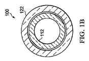
図1A及び図1Bには、本開示の教示による小型化された固体レーザ発振装置100の例が示されている。固体レーザ発振装置100は、第1の管104に取り付けられたマイクロチップ発振器(MCO)102と、第2の管108に取り付けられた体積ブラッグ格子(VBG)プレート106とを含んでおり、第2の管108は、スリップフィットで第1の管104内に入れ子式に挿入されるように構成されており、それによって、マイクロチップ発振器(MCO)102は、体積ブラッグ格子(VBG)プレート106と同心状に整列されるとともにVBGプレート106から特定の距離dに位置決めされる。
1A and 1B illustrate an example of a miniaturized solid
マイクロチップ振動レーザ(MCO)は、レーザ機器に広く用いられるようになってきたが、これらの機器を適切な構造でパッケージすることは、これまでの課題であった。示されるような固体レーザ発振装置100の特定の実施形態は、従来の固体レーザ発振装置の設計に対して1つ又は複数の利点を提供することができる。これらの利点は、シングルモードの短パルスレーザ発振を容易にするような固体レーザ発振装置100の熱的に独立した動作を含んでもよいことである。従来のレーザシステムは、典型的には、レーザダイオード光源とマイクロチップ発振器(MCO)とを使用しており、これら両者は、共通のヒートシンクに熱的に結合されていたが、本開示のマイクロチップ発振器(MCO)102と光発生源とで発生した熱勾配は、別々に消散される。従って、いずれかの構成要素の熱管理は、互いに独立して取り扱うことができる。別の利点は、不意のマルチモード及び/又は混合モードの動作を除外及び/又は低減させることができる。レーザ共振器内の温度変動によって、熱膨張係数(CTE)によって誘起された共振器内の空間変化がもたらされ、及びマイクロチップ発振器(MCO)の熱ストレスは、大抵の場合、マルチモード及び/又は混合モードの動作に影響を与える。マイクロチップ発振器(MCO)102によって生成される熱勾配の独立した管理は、これらの不意のマルチモード及び/又は混合モードの動作に対して改良された制御を提供することができる。また、固体レーザ発振装置100は、シングルモード光の波長が、生成された光ビームの波長又は位相同期を提供するために調整可能にされるようなパッケージを提供する。このような利点によって、固体レーザ発振装置100が、戦術的なレーザ送信機、光検出測距(LADAR)装置、空間センサシステム、空間用途レーザ、低質量近接ヒューズ等の各種レーザ用途に貢献することができる。さらに、提案された管状パッケージは、光学部品及びレーザ部品の内部汚染を防止又は低減するために光路をカプセル化する。
Microchip vibration lasers (MCOs) have been widely used in laser equipment, but packaging these equipments with an appropriate structure has been a challenge so far. Certain embodiments of the solid
マイクロチップ発振器(MCO)102は、周辺突合せ継手を使用して第1の管102の端面110に取り付けられる。この特定の実施形態では、マイクロチップ発振器(MCO)102は、1,064ナノメートル(nm)パルス光出力を生成するような、Nd3+YAG及びCr4+YAGの接合プレートと、誘電性コーティング(ミラー)とを含む。他の実施形態は、1,064nmよりも大きい又は未満の波長を有する光出力を生成してもよい。本明細書で説明するレーザ部品は、固相拡散接合によって製造された複合YAG結晶又はYAGセラミックユニットを含む。この構成により、Cr4+でドープされたYAG結晶は、複数の層を一緒に接合する際に、Nd3+YAGレーザ結晶の受動Qスイッチを提供する。具体的には、4価のCr4+でドープされたガーネットが、数マイクロ秒のパルス時間範囲で約1.0ミクロン(μm)の帯域幅の吸収を示す。1,064nmで発射するNd3+YAGレーザの場合では、Cr4+でドープされたYAGの吸収帯は、比較的低い飽和フルエンス(fluence)で反復的なQスイッチを可能にする。従って、Nd3+:YAG層及びCr4+:でドープされたYAG層を含む複合結晶は、1,064nmの発振のために比較的狭い帯域幅の供給源を形成することができ、この複合結晶は、受動Qスイッチングの高いピークパワーと高繰り返し速度のレーザパルスを抽出する。YAG接合プレートから形成されたマイクロチップ発振器(MCO)が示されているが、他のタイプの構成を有する他の材料から形成された他の実施形態を利用してもよい。
A microchip oscillator (MCO) 102 is attached to the
体積ブラッグ格子(VBG)プレート106は、周辺突合せ継手を使用して第2の管108の端面112に取り付けられる。体積ブラッグ格子(VBG)プレート106は、ファブリペロー型の単一のガラス板の光取出し(outcoupling)手段等の任意の適切なタイプを含んでもよい。一実施形態では、体積ブラッグ格子(VBG)プレート106は、体積ブラッグ格子(VBG)ガラス板を含んでもよい。体積ブラッグ格子(VBG)プレートは、フォトサーモグラフィ屈折ガラス材料から製造されており、且つ低パワー用途及び高パワー用途の両方に用いることができる。さらに、体積ブラッグ格子(VBG)プレートが作製される材料は、第2の管108のCTEに比較的似たCTEを有することができ、それによって、残留ストレスによる第2の管108の長さへの影響を最小限にすることができる。マイクロチップレーザと体積ブラッグ格子(VBG)装置とのマイクロ光学スタイルのハイブリッド化は、モードの数を1つの主要モードと1つの調整モードとに減らすことができるような、狭スペクトルで且つ高効率の出力能力を提供する。スペクトルの狭小化及び均一なスペクトル同調が、マイクロチップと体積ブラッグ格子(VBG)との間に所定の間隔で適切なマイクロチップ/体積ブラッグ格子(VBG)パッケージのハイブリッド化によって達成することができる。他の実施形態では、体積ブラッグ格子(VBG)プレート106は、他の材料で作製してもよい。
Volume Bragg grating (VBG)
一実施形態では、第1の管104及び第2の管108は、比較的高いレベルの透明性を有する溶融シリカから作製することができ、こうして分離された(decoupled)光が脱出できるようになる。第1の管104及び第2の管108は、生成された全ての熱流束をシンクするためにマイクロチップ発振器(MCO)102及び体積ブラッグ格子(VBG)プレート106よりも実質的に大きな質量を有してもよい。溶融シリカを組み込んだ特定の実施形態では、この溶融シリカの材料が、取り付けられるマイクロチップ発振器(MCO)102と体積ブラッグ格子(VBG)プレート106とのCTEに比較的似たCTEを有するという利点を提供することができる。さらに、第1の管104及び第2の管108内部のレーザ共振器は、主要な光軸線を中心に対称であるが、接合部は、主要な光軸線の周囲に配置されている。このように、物理的特性を、大きな温度変動に亘って比較的一貫して維持することができる。
In one embodiment, the
動作時に発生する熱流束を管理する熱機械設計上の特徴に加えて、シングルモード動作を提供するために、体積ブラッグ格子(VBG)プレート106の有効な格子は、マイクロチップ発振器(MCO)の端面に対して平行でありそのMCOの端面の軸線に対して垂直にする必要がある。約2〜5ミリメートルの全体的な寸法を有する市販の角柱状又は円盤状のマイクロチップ発振器(MCO)と一緒に使用される場合に、体積ブラッグ格子(VBG)プレート106の軸線方向のアライメントは、20〜200μmの間隔許容範囲で、体積ブラッグ格子(VBG)プレート106及びマイクロチップ発振器(MCO)102の位置決めにおいて約1.0μmの精度を必要とする場合がある。第1の管104内への第2の管108の摩擦嵌め及び間隙が制御された入れ子式の嵌合は、このレベルの精度を与えることができる。
In addition to the thermomechanical design features that manage the heat flux generated during operation, to provide single mode operation, the effective grating of the volume Bragg grating (VBG)
マイクロチップ発振器(MCO)102と体積ブラッグ格子(VBG)プレート106とを、任意の適切な方法で、それぞれ第1の管104及び第2の管108に取り付けることができる。一実施形態では、マイクロチップ発振器(MCO)102、体積ブラッグ格子(VBG)プレート106、第1の管104及び第2の管108が、相溶性を有する熱膨張係数(CTE)を有する場合に、高弾性エポキシ接合を用いることができる。熱膨張係数がミスマッチのアセンブリの場合には、低ストレス接着接合が、低ヤング率を有する熱加硫(RTV)シリコーンによって提供される。別の実施形態では、マイクロチップ発振器(MCO)102及び体積ブラッグ格子(VBG)プレート106を、第1の管104及び第2の管108に確実に取り付けることが、一緒にハンダ付けされるようなマイクロチップ発振器(MCO)102、体積ブラッグ格子(VBG)プレート106、第1の管104及び第2の管108上に形成された金属化表面によって実現することができる。これらの両方の場合において、接合部品及び保持ユニットの熱的な偏位(excursion)は、レーザ性能が、少なくとも部分的に又は殆どストレスに依存せず独立するように無視できる。特定の実施形態では、光軸線に対して周囲に存在するはんだ付け接合及び接着結合は、有機物を含まない光路を提供することができる。
A microchip oscillator (MCO) 102 and a volume Bragg grating (VBG)
入れ子式の及び周辺突合せ継手は、それらの隣接する面が、構造体の軸線の周りに実質的に延びているという意味で周辺である。この周辺構造によって、レーザ共振器の熱伸長を最小化することができ、こうして、比較的温度に依存しない動作を比較的ストレスフリーのアセンブリに提供することができる。完全にカプセル化され、保護された光路によって、埃や空気中を浮遊するデブリ等の少なくともいくつかは、殆ど、又は全ての不要な汚染が排除される。示される構成では、電界、温度場、及びストレス場は、軸対称性及び分離によって特徴付けられる。すなわち、光信号は、軸線方向に移動するように構成されるが、周囲の物理的ストレスは、軸線周りの半径方向の周縁に維持される。また、長手方向軸線に近い熱で誘起された偏位は、従って、軽減され得る。 Nested and peripheral butt joints are peripheral in the sense that their adjacent surfaces extend substantially around the axis of the structure. With this peripheral structure, the thermal elongation of the laser resonator can be minimized, thus providing a relatively temperature-independent operation for a relatively stress-free assembly. A fully encapsulated and protected light path eliminates most or all unwanted contamination of at least some such as dust and debris floating in the air. In the configuration shown, the electric field, temperature field, and stress field are characterized by axial symmetry and separation. That is, the optical signal is configured to move in the axial direction, but the surrounding physical stress is maintained at the radial periphery around the axis. Also, heat induced excursions near the longitudinal axis can therefore be mitigated.
一実施形態では、金属との酸化物のストレスフリー及びボイドフリーのインターフェイスの作製は、マイクロチップ発振器(MCO)102及び体積ブラッグ格子(VBG)プレート106をそれぞれの管に対してはんだ付け又はろう付けする前に、YAG結晶(YAGセラミック又はガラス)の金属化によって達成される。YAG結晶(YAGセラミック又はガラス)の乏しい濡れ性を克服するために、その合わせ面を活性化し、表面改質を施してもよい。表面活性化及び表面改質は、接合部品の汚染除去、その後の金属化を含むレーザ部品における合わせ面のNイオンプラズマ支援注入、Cu−W及び/又はCu−Mo焼結複合材料でコーティングされたレーザ部品のはんだ付け又はろう付けを含んでもよく、YAG材料は、取り付けられる管に一致するCTEである。
In one embodiment, the creation of an oxide-to-metal stress-free and void-free interface involves soldering or brazing the microchip oscillator (MCO) 102 and volume Bragg grating (VBG)
Nイオンプラズマ支援注入を、真空中で行ってもよい。従来のコーティングを行うための真空チャンバには、Nイオン放出源がさらに備えられている。注入技術は、結晶、セラミック、及びガラスの合わせ面を改質し且つ活性化するが、消費した酸素を補償し、濡れ性を向上させ、レーザ発振による酸化物材料と金属コーティングとの相互作用を向上させる。この接合技術は、形成されたはんだプールにおけるボイド形成を最小限に抑え、こうして効率的な界面熱伝達を与える。金属化は、注入後直ぐに開始され、真空中で同じコーティングチャンバ内で行われる。YAG結晶(又はセラミックス)とCu−W複合材料のヒートスプレッダとの融合に使用される低温共晶はんだ(例えば63/37 錫/鉛(Sn/Pb)又は60/40 錫/鉛合金)の特定のケースでは、金属化コーティングが、順次に堆積されたバインダー(すなわち、クロム(Cr)、チタン(Ti)、又はCr/Tiの組み合わせ)により、機能性金属(すなわち、ニッケル(Ni)及び金(Au))と一緒に形成される。これらの材料は、選択されたはんだと冶金学的に相溶性を有する。このように、固体レーザ発振装置100は、精密なレーザ共振器のための入れ子式の配置と、シングルモード短パルスレーザ発振のための精密な条件出しを容易にする熱ストレス管理機能とを有するような革新的で且つ効率的な光ファイバ型パッケージプラットフォームを含む。
N ion plasma assisted implantation may be performed in a vacuum. The vacuum chamber for performing the conventional coating is further provided with an N ion emission source. Implant technology modifies and activates the crystal, ceramic, and glass mating surfaces, but compensates for the oxygen consumed, improves wettability, and allows the laser to interact with the oxide material and the metal coating. Improve. This joining technique minimizes void formation in the formed solder pool, thus providing efficient interfacial heat transfer. Metallization begins immediately after implantation and takes place in the same coating chamber in a vacuum. Specific of low temperature eutectic solder (eg 63/37 tin / lead (Sn / Pb) or 60/40 tin / lead alloy) used for fusing YAG crystals (or ceramics) with Cu-W composite heat spreaders In the case, the metallized coating is applied to functional metals (ie, nickel (Ni) and gold (Au) by sequentially deposited binders (ie, chromium (Cr), titanium (Ti), or Cr / Ti combinations)). )). These materials are metallurgically compatible with the selected solder. As described above, the solid-state
図1には、固体レーザ発振装置100の一例が示されているが、種々の変更を、図1の実施形態に対して行ってもよい。例えば、体積ブラッグ格子(VBG)プレート106は、マイクロチップ発振器(MCO)からの光を調整して、任意の適切なモードの動作を生成するような任意のタイプの格子プレートであってもよい。さらに、第1の管104及び/又は第2の管108は、光軸線の向きを提供し、且つ固定前に適切なクロック同期を容易にするような平坦な表面輪郭で構成してもよい。
Although FIG. 1 shows an example of the solid-state
図2には、本開示の教示による小型化された固体レーザ発振装置200の別の例が示されている。図1の固体レーザ発振装置100と同様に、固体レーザ発振装置200は、第1の管204に取り付けられたマイクロチップ発振(MCO)装置202と、第2の管208に取り付けられた体積ブラッグ格子(VBG)プレート206とを含み、この第2の管208は、入れ子式の(スリップ)フィットで第1の管204に入れ子式に挿入されるように構成される。固体レーザ発振装置200は、コリメートされた光ファイバアセンブリ(光ファイバピグテール)214が構成されるような第3の管212を有する。第3の管212は、第1の管204の反対側の端部内に入れ子式に挿入されるように構成されており、それによって、光ファイバ入力アセンブリは、マイクロチップ発振器(MCO)202と体積ブラッグ格子(VBG)プレート206とに同軸に整列される。固体レーザ発振装置200は、第1のレンズ216と、第1の管204内に構成された第2のレンズ218とを含む。
FIG. 2 illustrates another example of a miniaturized solid
第1の管204と第2の管208とが、比較的精密な軸線方向のアライメントを提供するために、十分な寸法許容範囲で入れ子式の継手を形成して、マイクロチップ発振器(MCO)202と体積ブラッグ格子(VBG)プレート206との間に特定の空間を実現する。同様に、第1の管204と第3の管212とが、別の入れ子式の継手を形成して、マイクロチップ発振器(MCO)202と体積ブラッグ格子(VBG)プレート206とに対して光ファイバアセンブリ214の比較的精密な軸線方向のアライメントを提供する。特定の実施形態では、入れ子式の継手は、互いに対して回転可能であり、体積ブラッグ格子(VBG)プレート206と光ファイバアセンブリ214とに対してマイクロチップ発振器(MCO)202の小さな角度アライメントを提供する。
A
マイクロチップ発振器(MCO)202が、第1の管204に取り付けられており、体積ブラッグ格子(VBG)プレート206が、周辺突合せ継手を使用して第2の管208に取り付けられており、この突合せ継手によって、マイクロチップ発振器(MCO)と体積ブラッグ格子(VBG)プレートの構成部材を、入れ子式に形成されたアセンブリ内の内管と外管とへの確実な取り付けることが提供される。突合せ継手は、取り付けられたアセンブリの完全な中心決めを解決するようにマイクロチップと体積ブラッグ格子(VBG)プレートとの横方向の小さな並進移動を与えることができる。
A microchip oscillator (MCO) 202 is attached to the
管204,208,212は、透明なガラス材料等の任意の適切な材料で形成することができる。透明で低吸収性のガラス管204,208,212は、固体レーザ発振装置の適切な動作に有害な蛍光のパージを提供する。光ファイバパッケージ及び光ファイバーピグテールで広く使用されている市販のガラス製毛細管ユニットは、固体レーザ発振装置200の製造のための完全に適用可能であることに留意されたい。
The
蛍光の不利な影響は、レーザ部品のガラスカプセル化によって解決される。レーザ共振器内に形成される局所的な熱流束及び付随する温度勾配は、その形状及び寸法に応じて、高い熱質量及び急速熱時定数の筐体内で等化される。コンパクトなマイクロチップレーザは、小さな熱質量を有しているので、発生した熱勾配は、熱拡散性管状筐体ユニットによって再配分され且つ部分的にヒートシンクされることに留意されたい。既に再配分され且つ実質的に低減された熱流束及び付随する温度勾配は、能動又は受動ヒートシンク装置にさらに伝達させることができる。ヒートシンクの配置は、消費した総出力、マイクロチップの半径方向の熱勾配、熱時定数に基づいて構成することができ、且つマイクロチップと出力カプラとの間の間隔の変化で誘起されるCTE(熱膨張係数)をさらに最小限に抑えるように構成することができる。様々な結晶、セラミック、又はガラスの構成要素の接合に加えて、この技術は、寄生振動の比較的良好な界面抑制をレーザ利得媒質に提供する一方、反射、散乱、共鳴、熱偏位、ストレスによって誘起される二重屈折性を減少させる。熱的に管理可能なレーザアセンブリとYAG結晶(例えば、YAGセラミック又はガラス)とにおける界面伝導性の改善は、大抵の場合に、その合わせ面上に堆積した金属コーティングを使用する。YAG成形部材の金属でコーティングされた合わせ面が、次に金属又は伝導性複合材のヒートシンクにはんだ付け又はろう付けされる。形成されたはんだプールは、ボイドフリーの状態に製造され、界面導電性をさらに低減させるような可能な金属間の形成が低減される。また、提案する手法は、CTEが一致する酸化物及び金属材料を接合することのみに焦点を当てている。全体的な及び局所的なミスマッチストレスが、接着性及び接合性(接着剤及び/又ははんだ付け)材料の適切な材料選択と寸法設計とによって低減される。(温度依存性)のミスマッチ差は、上述した設計上の特徴によっても低減される。構成材料同士の間の熱膨張のミスマッチ差は、アセンブリ内のたわみと層間剥離の不具合の可能性をもたらすことに留意されたい。結晶組成(例えば、セラミック又はガラス)や金属が、ある特定の温度で熱的に一致している場合であっても、それらの熱的ミスマッチ差は、製造及び動作サイクル以内に制限される。従って、実現可能な接合技術の中でも、低温はんだ付け及びろう付けが、CTEが一致する接着レーザ及び熱管理ユニットのために使用される。 The disadvantageous effect of fluorescence is solved by glass encapsulation of the laser component. Depending on its shape and dimensions, the local heat flux formed in the laser cavity and the associated temperature gradient are equalized in a housing with a high thermal mass and a rapid thermal time constant. Note that since the compact microchip laser has a small thermal mass, the generated thermal gradient is redistributed and partially heatsinked by the heat diffusing tubular housing unit. Already redistributed and substantially reduced heat fluxes and associated temperature gradients can be further transmitted to active or passive heat sink devices. The heat sink arrangement can be configured based on the total power consumed, the radial thermal gradient of the microchip, the thermal time constant, and the CTE (induced by the change in the spacing between the microchip and the output coupler). The thermal expansion coefficient) can be further minimized. In addition to joining various crystal, ceramic, or glass components, this technique provides relatively good interface suppression of parasitic oscillations to the laser gain medium, while reflecting, scattering, resonance, thermal excursions, stress Reduces the birefringence induced by. Improvements in interfacial conductivity in thermally manageable laser assemblies and YAG crystals (eg, YAG ceramics or glass) often use a metal coating deposited on the mating surfaces. The metal-coated mating surfaces of the YAG molded part are then soldered or brazed to a metal or conductive composite heat sink. The formed solder pool is manufactured in a void free state, reducing possible metal-to-metal formation that further reduces interfacial conductivity. Also, the proposed approach focuses only on joining oxides and metal materials with matching CTEs. Overall and local mismatch stress is reduced by proper material selection and dimensional design of adhesive and bondable (adhesive and / or soldering) materials. The mismatch difference in (temperature dependence) is also reduced by the above-described design characteristics. It should be noted that the thermal expansion mismatch difference between the constituent materials leads to possible deflection and delamination failures within the assembly. Even when crystalline compositions (eg, ceramic or glass) and metals are thermally matched at a particular temperature, their thermal mismatch difference is limited within manufacturing and operating cycles. Thus, among possible bonding techniques, low temperature soldering and brazing are used for bonded lasers and thermal management units with CTE matching.
孔220は、第2の管208を第1の管204に接合するための接着剤を挿入するために第1の管204に形成される。さらに、別の孔222が、第3の管212を第1の管204に接合するための接着剤を挿入するために第1の管204に形成される。透明な材料を使用する特定の実施形態は、多くのマイクロオプトエレクトロニクス・アセンブリに特有の「ブラインド(blind)」アセンブリの特性を緩和し、完成したレーザの下流側の品質検査を容易にすることができる。
A
2つのレンズ216,218は、光ビームを集束させるために使用される。レンズ216は、反射防止(AR)コーティングされ、且つ成形プリフォームから作製される。レンズ216は、励起光をフォーマットする。レンズ216は、その平坦面に見当(位置)合わせされ且つマイクロチップ発振器(MCO)のカートリッジ管内に非熱的に接合される。レンズ216の外側面及び管状筐体穴の内面は、比較的精密な入れ子式の継手を形成する。この構成により、CTEの場合であっても、管に使用されるCTEがミスマッチしたガラスは、過度の横方向変位がなくなるようにすることができる。
Two
レンズ218は、スペーサ226を用いてレンズ216から分離されている。スペーサ226は、適切な低CTE合金から製造することができる。レンズ218は、成形プリフォームから製造されてもよく、反射防止(AR)コーティングを備えてもよい。レンズ218はまた、励起光をフォーマットする。レンズ218は、第3の管212に取り付けられ、第3の管212に非熱的に接合される。
The
図2には、小型化された固体レーザ発振装置200の一例が示されているが、種々の変更を、図2の実施形態に対して行ってもよい。例えば、管は、任意の適切なタイプの材料から形成することができる。特定の例として、第1の管204、第2の管208、及び第3の管212のそれぞれは、比較的似たCTEを提供するような材料の組み合わせで形成することができる。さらに、管は、所望の寸法の許容範囲を満たすように機械加工された比較的安価な毛細管プリフォームから作製することができる。
Although FIG. 2 shows an example of a miniaturized solid-state
図3A及び図3Bには、それぞれ、本開示の一実施形態による励起ダイオード316に結合された固体レーザ発振装置300の例の斜視図又は分解図が示されている。図1の固体レーザ発振装置100と同様に、固体レーザ発振装置300は、第1の管304上に配置されたマイクロチップ発振器(MCO)302と、第2の管308上に配置された体積ブラッグ格子(VBG)プレート306と、入れ子式の(スリップ)フィットを用いて一緒に結合することができる第3の管312上に配置された光ファイバアセンブリ314と、を含む。固体レーザ発振装置300は、第1の管304上に配置されたいくつかのヒートシンク要素318を含んでもよい。示される概観は、比較的コンパクトなレーザをもたらすような、構成要素の軸線方向及び半径方向のアセンブリ配置を示す。示される全体的なパッケージのサイズは、約2.54センチメートル(cm)(1.0インチ)の直径×7.62cm(3.0インチ)の長さで、56.70グラム(2オンス)未満の重量である。他の実施形態は、本明細書で説明するサイズ及び重量とは異なる次元のサイズ及び重量を有してもよい。
3A and 3B show a perspective view or an exploded view of an example of a solid
この特定の実施形態のヒートシンク要素318は、マイクロチップ発振器(MCO)302によって生成された熱や熱エネルギーを吸収するペルチェ素子として一般的に知られている熱電クーラー(TEC)を有する。効率的な市販のサーマルプレート・スプレッダーは、比較的に小さな熱流束の大きさによって適用可能である。さらに、示される固体レーザ発振装置300は、3つのTECを含むが、他の実施形態は、3つより多くの又は3つ未満のTECを含んでもよい。ヒートシンク要素318は、ガラス管状ユニットの外面上に対称的に配置されており、且つ第1の管302上に位置決めされて、比較的短い熱伝導経路をマイクロチップ発振器(MCO)302に提供する。ヒートシンク要素318は、第1の管302の周囲の平坦面に取り付けられる。このように、光吸収性のマイクロチップ発振器(MCO)302によって生成された熱勾配は、固体レーザ発振装置300の軸線に沿って、概して同軸方向モード及び半径方向(redial)支配モードで消散されてもよい。さらに、ヒートシンク要素318は、マイクロチップ発振器(MCO)302の比較的近くに配置することができる。このような配置を有する特定の実施形態は、温度変動による比較的少ないスペクトル変形を含むようなシングルモードの動作で動作する能力を保持することができる。さらに、このような実施形態は、レーザ共振器の温度によって誘起された伸張又は収縮に対して比較的鈍感(無反応)であり得る。従って、パッケージの半径方向の対称性は、異なる温度レベルで保存することができる。これは、シングルモード動作について比較的重要な特徴である。
The
特定の実施形態は、レーザ出力スケーリングを提供することによって、変動する出力レベルで発生する熱を効率的に放散するような利点を提供することができる。また、マイクロチップ発振器(MCO)302からヒートシンク要素318への主要な半径方向の短い熱伝導経路は、典型的には、レーザ発振特性に変動を引き起こすような、利得媒体内の温度変化及び温度勾配を緩和する。さらに、透明な管304,306,312によって、蛍光が管内の共振器を過熱することなく脱出することが可能になる。フェルール(口金)オプションを越えて延びるような、示される光ファイバ接続オプションは、多重化された励起装置及び/又は遠隔の励起取付具(マウント)を収容することができる。また、管304,306,312は、比較的厚い壁で構成されており、光路の方向に対して半径方向及び軸線方向の両方で、熱によって誘起されるストレスを低減することができる。
Certain embodiments can provide advantages such as efficiently dissipating heat generated at varying power levels by providing laser power scaling. Also, the main radial short heat conduction path from the microchip oscillator (MCO) 302 to the
図3A及び図3Bには、励起ダイオード316に結合された、小型化された固体レーザ発振装置300の一例が示されているが、種々の変更を図3A及び図3Bに示される実施形態に対して行ってもよい。例えば、励起ダイオード316は、固体レーザ発振装置300による使用に適した光の列を発生させるような任意のタイプの光発生装置を含むことができる。さらに、ヒートシンク要素318は、マイクロチップ発振器(MCO)302からの熱を積極的に放散させるようなTECとして示されているが、他の実施形態は、受動ヒートシンク要素(例えば、熱スプレッダ)等の熱を放散するような任意の適切なタイプのヒートシンク要素を含んでもよい。
FIGS. 3A and 3B show an example of a miniaturized solid
図4A、図4B、及び4Cには、本開示の教示による小型化された固体レーザ発振装置上に配置された取付構造の例が示されている。図3A及び図3Bの固体レーザ発振装置300と同様に、固体レーザ発振装置402の光ファイバーアセンブリ402は、光ファイバ406を使用する励起ダイオード404に結合されている。
図4Aの実施形態は、管状部材412を有する金属ブロック410を含んでおり、この金属ブロック410は、固体レーザ発振装置402と、別の構造体に取り付けるための孔を有するフランジ414とを収容する。
4A, 4B, and 4C show examples of mounting structures disposed on a miniaturized solid state laser oscillator according to the teachings of the present disclosure. Similar to the solid
The embodiment of FIG. 4A includes a metal block 410 having a
図4Bの実施形態は、上部材422を有する金属ブロック420を含んでおり、この上部材422は、固体レーザ発振装置402を保持するための底部材424にボルトで固定される。底部材424は、別の構造体に取り付けるための孔を有するフランジ426を含んでもよい。底部材424は、固体レーザ発振装置402に弾性結合するのための内部スプリング(図示せず)を含むV字型のサドルを有する。この配置では、光ファイバ相互接続部の予め選択された長さによって、熱的に誘起される変位を含むような、ほぼストレスフリーの変位が可能になる。比較的大きな熱質量を有するので、底部材424のV字型のサドルは、固体レーザ発振装置402上に分布した物理的ストレスを比較的均一にする。さらに、その円筒形状のフォームファクタは、用途と、特定のレーザシステムのパッケージ制約とに応じて調整可能な取付けを提供する。
The embodiment of FIG. 4B includes a
図4Cには、固体レーザ発振装置402と一緒に図4Bの金属ブロック420上に取り付けられた受動ヒートシンク430が示されている。ヒートシンク430は、伝導性接着剤を使用して、アセンブリの発熱領域に接合されており、固体レーザ発振装置402との界面全体の温度上昇を最小限に抑えることができる。
これらの特定の実施形態は、少なくとも部分的に、又は殆ど断熱化されるような取付け構造を提供することができる。金属ブロック410,420を用いて、励起ダイオード404と固体レーザ発振装置402との間の光ファイバ相互接続の構造パラメータは、比較的良好な構造的一体性を提供する一方、光ファイバの比較的小さい曲率に起因する光損失を低減する。
FIG. 4C shows a
These particular embodiments can provide an attachment structure that is at least partially or substantially thermally insulated. With
図4A、図4B、及び図4Cには、固体レーザ発振装置402を取り付けるために使用される取付構造のいくつかの例が示されているが、各種の変更を、図4A、4B、及び4Cに示される実施形態に対して行ってもよい。例えば、取付構造は、固体レーザ発振装置402上に配置されたヒートシンク要素に熱的結合させるための1つ又は複数の追加要素を含んでもよい。さらに、取付構造体は、ハウジングから伝達される物理的ショック及び振動エネルギーを低減するようなゴムグロメット等の取付構造も含み、この取付構造は、固体レーザ発振装置402に取り付けられている。
4A, 4B, and 4C show some examples of mounting structures used to mount the solid
図5には、本開示の一実施形態による小型化された固体レーザ発振装置を製造するためのプロセス500の例が示されている。
ステップ502において、マイクロチップ発振器(MCO)は、第1の管の端面に位置決めされており、且つマイクロ波溶融金属化層又は従来のはんだ付けプロセスを使用して第1の管に接合されている。一実施形態では、マイクロチップ発振器(MCO)は、空気硬化、熱硬化、又は化学硬化接着剤を使用して第1の管に接合してもよい。
FIG. 5 shows an example of a
In step 502, a microchip oscillator (MCO) is positioned at the end face of the first tube and joined to the first tube using a microwave molten metallization layer or a conventional soldering process. . In one embodiment, a microchip oscillator (MCO) may be joined to the first tube using an air cured, heat cured, or chemical cured adhesive.
ステップ504において、集束レンズは、光ファイバーアセンブリを用いて構成された第3の管内に接合される。1つ以上のスペーサは、互いに、且つ管の軸線に対して適切な位置を確保するために2つのレンズの間に挿入することができる。一実施形態では、アライメント及び光スポット像は、第1の管を介してサンプルビーム光を注入するようなターゲット固定具を使用して確立することができる。
ステップ506において、図5Bからの第3の管が、図5Aからの第1の管に挿入される。これらの管を互いに整列した後で、それらの管は、第1の管に配置された孔から注入された接着剤を用いて互いに接合してもよい。
In step 504, the focusing lens is bonded into a third tube constructed using an optical fiber assembly. One or more spacers can be inserted between the two lenses to ensure proper positioning relative to each other and to the tube axis. In one embodiment, the alignment and light spot image can be established using a target fixture such as injecting sample beam light through the first tube.
In
ステップ508において、体積ブラッグ格子(VBG)プレートは、第2の管に取り付けられる。一実施形態では、第2の管は、格子方向を参照するために、体積ブラッグ格子(VBG)プレートを固体レーザ発振装置に半径方向に整列させるようなクロック同期フラット部を含むことができる。
ステップ510において、第2の管は、第1の管内に挿入され且つ整列され、適切な接着剤を用いて接合される。また、ヒートシンクは、適切な接合用接着剤を使用して、第1の管に取り付けることができる。第1の管を第2の管に接合する前に、アライメントは、励起ダイオードに電力を供給することにより行われる一方、所望のレーザ発振モードが達成されるとともに経時的に比較的安定したシングルモードになるまで、体積ブラッグ格子(VBG)プレートを位置決めする。その後、固体レーザ発振装置の製造プロセスが完了する。
In
In step 510, the second tube is inserted and aligned within the first tube and joined using a suitable adhesive. The heat sink can also be attached to the first tube using a suitable bonding adhesive. Prior to joining the first tube to the second tube, alignment is performed by supplying power to the excitation diode, while the desired lasing mode is achieved and the single mode is relatively stable over time. Position the volume Bragg grating (VBG) plate until. Thereafter, the manufacturing process of the solid-state laser oscillation device is completed.
図5には、小型化された固体レーザ発振装置を製造するための方法500の一例が示されているが、各種の変更を、図5に示される実施形態に対して行ってもよい。例えば、一連のステップとして示されるように、図5の各種ステップを、重複するように行う、並列に行う、異なる順序で行う、又は複数回行ってもよい。
Although FIG. 5 shows an example of a
図6には、本開示の一実施形態による光学アセンブリ600の例が示されている。光学アセンブリ600は、2つの対応する光ファイバ606及びカプラ608介して励起ダイオード等の2つの光発生装置604に光学的に結合された小型化された固体レーザ発振装置602を有する。スプール610は、光ファイバ606をコイル形状に保持するためのフレームを提供する。
FIG. 6 illustrates an example
光発生装置604は、大抵の場合に、マイクロチップ発振器(MCO)が、固体レーザ発振装置602内に配置されている場合に、実質的により多くの熱を発生させる。従って、光学アセンブリ600は、固体レーザ発振装置602からの光発生装置604の物理的な分離を提供し、それによって、それら装置の熱放散を個別に管理することができる。さらに、固体レーザ発振装置602の熱放散は、シングルモード領域で適切な動作を提供するために、光発生装置604の精度より高いレベルの精度で管理する必要がある。光発生装置604に対して固体レーザ発振装置602を遠隔に取り付けることにより、温度に敏感なシングルモードのマイクロチップ発振器(MCO)/体積ブラッグ格子(VBG)構成要素を有する固体レーザ発振装置602レーザを、ダイオード・アセンブリ及びその分離したヒートシンクユニットから熱的に分離させる。スプール610は、光発生装置604用の取付構造を提供し、且つ光発生装置604用のヒートシンクを形成する。スプール610は、光ファイバケーブル606と取付/案内セグメントとの精密な位置決め用の埋め込み型V字溝機構を含むような熱伝導性合金から製造される。光ファイバの小さな熱質量に対するスプールの大きな熱質量によって、湾曲した光ファイバ内で発生する熱の効率的な熱スプレッダとなる。
The
カプラ608が、2つの光発生装置604によって生成された光ビームをまとめるために提供される。他の実施形態では、光学アセンブリ600は、1つの光発生装置又は2つ以上の光発生装置等の任意の適切な数の光発生装置(例えば、レーザ励起ダイオード)を有してもよい。例えば、バッテリは、本明細書に示されたものと同様の方法で円筒形状のスプールに取り付けられた4〜16個の光発生装置を有する。示されるような市販されているカプラは、適切なカプラの組み合わせ比の選択によりパワースケーリングを提供してもよい。この配置は、特定の又は指定の光発生装置から選択して光ビームを固体レーザ発振装置602内に注入してもよい。
A
図7には、本開示の一実施形態による別の例の光学アセンブリ700が示されている。図4Cの光学アセンブリと同様に、光学アセンブリは、金属ブロック704に配置された、受動ヒートシンク706に熱的に結合された、そして光ファイバ710のセクションを介して光発生装置708に光学的に結合された、小型化された固体レーザ発振装置702を有する。光学アセンブリ700は、励起光ビームをマイクロチップ発振器(MCO)のQスイッチ層に注入するような受動Qスイッチブリーチング(漂白)光発生装置712も含んでおり、パルス繰り返し周波数設定と精密なパルスタイミング制御のための固体レーザ発振装置においてレーザ共振器を光学的に漂白する。ブリーチング(漂白)光発生装置712は、上述したような方法で、熱管理のための一体型ヒートシンクに取り付けられる。
FIG. 7 illustrates another example
さらに、固体レーザ発振装置のレーザ共振器は、反射防止(AR)及びダイクロイック誘電コーティング等の高いレーザ損傷耐性を有する2つの誘電性干渉コーティング(ミラー)を含んでもよい。ダイクロイック干渉フィルタコーティングは、高反射及び反射防止(HR/AR)セグメントを含み、こうして、特定の波長を反射し(例えば、励起)、他の(動作)波長を透過させる。これらの両方のコーティングは、Ta205/SiO2フィルム等の高屈折率及び低屈折率の酸化物材料の干渉薄膜によって形成される。このタイプのフィルムは、比較的良好なレーザ損傷耐性を提供することができ、この耐性は、ブリーチング(漂白)レーザ励起ダイオード712のために特に重要である。
Further, the laser resonator of the solid state laser oscillation device may include two dielectric interference coatings (mirrors) having high laser damage resistance such as antireflection (AR) and dichroic dielectric coating. The dichroic interference filter coating includes highly reflective and antireflective (HR / AR) segments, thus reflecting certain wavelengths (eg, excitation) and transmitting other (operational) wavelengths. Both of these coatings are formed by interference films of high and low refractive index oxide materials such as Ta205 / SiO 2 films. This type of film can provide relatively good laser damage resistance, which is particularly important for bleaching
図7には、固体レーザ発振装置602を含む光学アセンブリ700の一例が示されているが、各種の変更を、図7の実施形態に対して行ってもよい。例えば、示される光発生装置712は、第1の管のポートホールを通してマイクロチップ発振器(MCO)のキャビティ内に漂白ビームを導入するような励起ダイオードを有しているが、光発生装置712は、取付構造体から遠隔に配置されており、且つ別の光ファイバ(図示せず)を介して固体レーザ発振装置702に光学的に結合してもよい。
Although FIG. 7 shows an example of an
取付構造は、固体レーザ発振装置402上に配置されるヒートシンク要素に熱的に結合させるための1つ又は複数の追加の要素を含んでもよい。さらに、取付構造は、ハウジングから伝達された物理的なショック及び振動エネルギーを低減させるようなラバーグロメット等の取付機構を含んでもよく、この取付構造は、固体レーザ発振装置402上に取り付けられる。
The mounting structure may include one or more additional elements for thermally coupling to a heat sink element disposed on the solid
本開示は、特定の実施形態及び一般的に関連する方法を説明するが、これらの実施形態及び方法の交換及び並べ替えが当業者には明らかであろう。従って、例示的な実施形態の上述した説明は、本開示を規定又は制限するものではない。以下の特許請求の範囲によって規定されるように、他の変更、置換、及び変更は、本開示の精神及び範囲から逸脱することなく可能である。 While this disclosure describes particular embodiments and generally associated methods, replacements and permutations of these embodiments and methods will be apparent to those skilled in the art. Accordingly, the above description of example embodiments does not define or constrain this disclosure. Other modifications, substitutions, and alterations are possible without departing from the spirit and scope of this disclosure, as defined by the following claims.
Claims (20)
第1の管に取り付けられたマイクロチップ発振器(MCO)と;
第2の管に取り付けられた体積ブラッグ格子(VBG)プレートであって、第2の管は、スリップフィットで第1の管に入れ子式に結合されるように構成されており、それによって、前記体積ブラッグ格子(VBG)プレートは、前記マイクロチップ発振器(MCO)と同心状に整列されるとともに該マイクロチップ発振器(MCO)から特定の距離に位置決めされる、体積ブラッグ格子(VBG)プレートと;を備える、
固体レーザ発振装置。 A solid-state laser oscillation device, the solid-state laser oscillation device:
A microchip oscillator (MCO) attached to the first tube;
A volume Bragg grating (VBG) plate attached to a second tube, wherein the second tube is configured to be telescopically coupled to the first tube in a slip fit, thereby A volume Bragg grating (VBG) plate, concentrically aligned with the microchip oscillator (MCO) and positioned at a specific distance from the microchip oscillator (MCO); Prepare
Solid state laser oscillator.
請求項1に記載の固体レーザ発振装置。 The first tube has an end face perpendicular to the axis of the first tube, and the microchip oscillator (MCO) is attached to the end face by a butt joint.
The solid-state laser oscillation device according to claim 1.
請求項1に記載の固体レーザ発振装置。 The second tube has an end face perpendicular to the axis of the second tube, and the volume Bragg grating (VBG) plate is attached to the end face by a butt joint;
The solid-state laser oscillation device according to claim 1.
請求項1に記載の固体レーザ発振装置。 The microchip oscillator (MCO) is attached to the end face including the metallization layer using at least one of metallization, soldering, or microwave melting processes.
The solid-state laser oscillation device according to claim 1.
請求項1に記載の固体レーザ発振装置。 And further comprising a heat sink disposed in a first tube configured to dissipate heat from the microchip oscillator (MCO), the heat sink comprising at least one of a Peltier element and a passive heat spreader. Have one,
The solid-state laser oscillation device according to claim 1.
請求項1に記載の固体レーザ発振装置。 The first tube and the second tube are made of transparent glass;
The solid-state laser oscillation device according to claim 1.
請求項1に記載の固体レーザ発振装置。 A third tube attached to the fiber optic input assembly is further provided, the third tube configured to be telescopically coupled to the first tube in a slip fit, whereby the light A fiber input assembly is concentrically aligned with the microchip oscillator (MCO);
The solid-state laser oscillation device according to claim 1.
請求項1に記載の固体レーザ発振装置。 A light generating device optically coupled to the solid state laser oscillator via an optical fiber, the light generating device dissipating heat different from heat dissipated by the microchip oscillator (MCO); Configured to
The solid-state laser oscillation device according to claim 1.
請求項8に記載の固体レーザ発振装置。 A spool configured to hold the optical fiber in a coil shape and to dissipate heat from the light generator;
The solid-state laser oscillation device according to claim 8.
請求項8に記載の固体レーザ発振装置。 The light generator has an excitation diode;
The solid-state laser oscillation device according to claim 8.
マイクロチップ発振器(MCO)を第1の管に取り付けるステップと;
体積ブラッグ格子(VBG)プレートを第2の管に取り付けるステップと;
スリップフィットで第1の管に第2の管を入れ子式に結合するステップであって、該結合するステップによって、前記体積ブラッグ格子(VBG)プレートは、前記マイクロチップ発振器(MCO)と同心状に整列されるとともに該マイクロチップ発振器(MCO)から特定の距離に位置決めされる、結合するステップと;を含む、
方法。 A method, the method being:
Attaching a microchip oscillator (MCO) to the first tube;
Attaching a volume Bragg grating (VBG) plate to the second tube;
Nesting a second tube in a slip fit with a first tube, the volume Bragg grating (VBG) plate concentrically with the microchip oscillator (MCO) by the coupling step Aligning and positioning at a specific distance from the microchip oscillator (MCO);
Method.
請求項11に記載の方法。 The step of attaching the microchip oscillator (MCO) to the first tube is a step of attaching the microchip oscillator (MCO) to the end surface of the first tube with a butt joint, wherein the end surface is connected to the first tube. Including a mounting step that is perpendicular to the axis;
The method of claim 11.
請求項11に記載の方法。 The microchip oscillator (MCO) is attached to the end face including a metallization layer using a microwave melting process;
The method of claim 11.
請求項11に記載の方法。 The step of attaching the volume Bragg grating (VBG) plate to the second tube is a step of attaching the volume Bragg grating (VBG) plate to the end surface of the second tube by a butt joint, wherein the end surface is a second tube. Mounting, being perpendicular to the axis of the tube,
The method of claim 11.
請求項11に記載の方法。 Disposing a heat sink for dissipating heat from the microchip oscillator (MCO) in a first tube, the heat sink having at least one of a Peltier element and a passive heat spreader;
The method of claim 11.
請求項11に記載の方法。 The first tube and the second tube are made of transparent and low light absorption glass;
The method of claim 11.
請求項11に記載の方法。 The method further includes attaching a third tube to the fiber optic assembly and telescopically coupling the third tube to the first tube in a slip fit, whereby the fiber optic input assembly includes the microchip oscillator ( Aligned concentrically with MCO),
The method of claim 11.
固体レーザ発振装置を備えており、該固体レーザ発振装置は:
第1の管に取り付けられたマイクロチップ発振器(MCO)と;
スリップフィットで第1の管に入れ子式に結合されるように構成された第2の管に取り付けられた体積ブラッグ格子(VBG)プレートであって、それによって、該体積ブラッグ格子(VBG)プレートは、前記マイクロチップ発振器(MCO)と同心状に整列されるとともに該マイクロチップ発振器(MCO)から特定の距離に位置決めされる、体積ブラッグ格子(VBG)プレートと;
光ファイバを使用して固体レーザ発振装置に光学的に結合された光発生装置であって、該光発生装置は、前記マイクロチップ発振器(MCO)によって放散される熱とは異なる熱を放散するように構成される、光発生装置と;を有する、
光発生システム。 A light generation system, which is:
A solid-state laser oscillation device, the solid-state laser oscillation device comprising:
A microchip oscillator (MCO) attached to the first tube;
A volume Bragg grating (VBG) plate attached to a second tube configured to be telescopically coupled to the first tube in a slip fit, whereby the volume Bragg grating (VBG) plate is A volume Bragg grating (VBG) plate that is concentrically aligned with the microchip oscillator (MCO) and positioned at a specific distance from the microchip oscillator (MCO);
A light generator optically coupled to a solid state laser oscillator using an optical fiber, the light generator dissipating heat different from that dissipated by the microchip oscillator (MCO) A light generating device, comprising:
Light generation system.
請求項18に記載の光発生システム。 The solid-state laser oscillation device further includes a spool configured to hold an optical fiber in a coil shape and to dissipate heat from the light generation device.
The light generation system according to claim 18.
請求項18に記載の光発生システム。 The light generator has an excitation diode;
The light generation system according to claim 18.
Applications Claiming Priority (3)
| Application Number | Priority Date | Filing Date | Title |
|---|---|---|---|
| US13/417,097 US9001862B2 (en) | 2012-03-09 | 2012-03-09 | Miniaturized solid-state lasing device, system and method |
| US13/417,097 | 2012-03-09 | ||
| PCT/US2013/021028 WO2013133909A1 (en) | 2012-03-09 | 2013-01-10 | Miniaturized solid-state lasing device, system, and method |
Publications (3)
| Publication Number | Publication Date |
|---|---|
| JP2015509668A true JP2015509668A (en) | 2015-03-30 |
| JP2015509668A5 JP2015509668A5 (en) | 2016-01-07 |
| JP6023223B2 JP6023223B2 (en) | 2016-11-09 |
Family
ID=49114101
Family Applications (1)
| Application Number | Title | Priority Date | Filing Date |
|---|---|---|---|
| JP2014560914A Active JP6023223B2 (en) | 2012-03-09 | 2013-01-10 | Miniaturized solid state laser oscillation device, system, and method |
Country Status (5)
| Country | Link |
|---|---|
| US (1) | US9001862B2 (en) |
| EP (1) | EP2823538B1 (en) |
| JP (1) | JP6023223B2 (en) |
| IL (1) | IL234213B (en) |
| WO (1) | WO2013133909A1 (en) |
Cited By (2)
| Publication number | Priority date | Publication date | Assignee | Title |
|---|---|---|---|---|
| JP2016219712A (en) * | 2015-05-25 | 2016-12-22 | 株式会社メガオプト | Multiwavelength laser oscillation device and multiwavelength laser oscillation method |
| JP2021100092A (en) * | 2019-12-19 | 2021-07-01 | 一哲 高橋 | Laser device |
Families Citing this family (5)
| Publication number | Priority date | Publication date | Assignee | Title |
|---|---|---|---|---|
| JP2017188596A (en) * | 2016-04-07 | 2017-10-12 | 三菱電機株式会社 | Optical module |
| US20200001423A1 (en) * | 2018-06-27 | 2020-01-02 | Edmund Optics, Inc. | Power polishing apparatuses and methods for in-situ finishing and coating of optical component |
| CN110423990A (en) * | 2019-09-03 | 2019-11-08 | 肇庆宏旺金属实业有限公司 | A kind of steel band coating system |
| US10907967B1 (en) | 2019-10-02 | 2021-02-02 | Honeywell International Inc. | Ring laser gyroscopes with active volume Bragg grating |
| US11947048B2 (en) | 2020-05-06 | 2024-04-02 | Waymo Llc | Crosstalk reduction for light detection and ranging (lidar) devices using wavelength locking |
Citations (8)
| Publication number | Priority date | Publication date | Assignee | Title |
|---|---|---|---|---|
| JPS62274788A (en) * | 1986-05-19 | 1987-11-28 | スペクトラ−フィジックス・インコ−ポレイテッド | Solid state laser which has small size quick mating/unmatingtype laser head and is pumped by laser diode |
| JPS6327080A (en) * | 1986-06-26 | 1988-02-04 | アモコ・コ−ポレ−ション | Solid state laser and manufacture of the same |
| JPH0246410A (en) * | 1988-06-29 | 1990-02-15 | American Teleph & Telegr Co <Att> | Optoelectronics organizer/former |
| JPH0688912A (en) * | 1991-09-19 | 1994-03-29 | Eastman Kodak Co | Attaching device for optical fiber and laser diode |
| JPH06511600A (en) * | 1991-05-08 | 1994-12-22 | ラディアンズ イノーバ エー ビー | laser with external cavity |
| JP2007527616A (en) * | 2003-07-03 | 2007-09-27 | ピーディー−エルディー、インク. | Use of volume, Bragg, and grating to adjust laser emission characteristics |
| US7648290B2 (en) * | 2005-09-20 | 2010-01-19 | Jds Uniphase Corporation | Modular solid-state laser platform based on coaxial package and corresponding assembly process |
| JP2011014646A (en) * | 2009-06-30 | 2011-01-20 | Ngk Spark Plug Co Ltd | Passive q-switched solid-state laser oscillator and laser ignition device |
Family Cites Families (14)
| Publication number | Priority date | Publication date | Assignee | Title |
|---|---|---|---|---|
| US4865436A (en) | 1986-03-25 | 1989-09-12 | Honeywell Inc. | Low cost ring laser angular rate sensor |
| US4723257A (en) * | 1986-05-19 | 1988-02-02 | Spectra-Physics, Inc. | Laser diode pumped solid state laser with miniaturized laser head |
| US4734912A (en) * | 1986-06-06 | 1988-03-29 | Lightwave Electronics Corp. | Laser diode end pumped Nd:YAG single mode laser |
| DE19723269A1 (en) * | 1997-06-03 | 1998-12-10 | Heidelberger Druckmasch Ag | Solid state lasers with one or more pump light sources |
| US6055815A (en) | 1998-10-30 | 2000-05-02 | Litton Systems, Inc. | Temperature-controlled microchip laser assembly and associated submount assembly |
| JP2002182073A (en) | 2000-12-11 | 2002-06-26 | Nippon Sheet Glass Co Ltd | Light source-optical fiber coupler |
| US6811916B2 (en) * | 2001-05-15 | 2004-11-02 | Neah Power Systems, Inc. | Fuel cell electrode pair assemblies and related methods |
| EP1670933A4 (en) | 2003-09-22 | 2008-01-23 | Snake Creek Lasers Llc | High densiity methods for producing diode-pumped micro lasers |
| US7590160B2 (en) | 2004-11-26 | 2009-09-15 | Manni Jeffrey G | High-gain diode-pumped laser amplifier |
| CA2634632A1 (en) | 2005-12-28 | 2007-07-05 | Bioscan Ltd. | Opto-electronic system and method for detecting perturbations |
| US20090059980A1 (en) * | 2007-03-16 | 2009-03-05 | Braun Alan M | High-stability frequency reference based on self-locked alkali-vapor laser |
| KR101458077B1 (en) | 2008-05-01 | 2014-11-04 | 삼성전자 주식회사 | Light Emitting Device and Preparing Method thereof |
| US8295320B2 (en) | 2009-05-26 | 2012-10-23 | Redfern Integrated Optics, Inc. | Achieving low phase noise in external cavity laser implemented using planar lightwave circuit technology |
| US8483248B2 (en) * | 2010-09-14 | 2013-07-09 | Raytheon Company | Laser crystal components joined with thermal management devices |
-
2012
- 2012-03-09 US US13/417,097 patent/US9001862B2/en active Active
-
2013
- 2013-01-10 WO PCT/US2013/021028 patent/WO2013133909A1/en active Application Filing
- 2013-01-10 EP EP13757321.8A patent/EP2823538B1/en active Active
- 2013-01-10 JP JP2014560914A patent/JP6023223B2/en active Active
-
2014
- 2014-08-20 IL IL234213A patent/IL234213B/en active IP Right Grant
Patent Citations (8)
| Publication number | Priority date | Publication date | Assignee | Title |
|---|---|---|---|---|
| JPS62274788A (en) * | 1986-05-19 | 1987-11-28 | スペクトラ−フィジックス・インコ−ポレイテッド | Solid state laser which has small size quick mating/unmatingtype laser head and is pumped by laser diode |
| JPS6327080A (en) * | 1986-06-26 | 1988-02-04 | アモコ・コ−ポレ−ション | Solid state laser and manufacture of the same |
| JPH0246410A (en) * | 1988-06-29 | 1990-02-15 | American Teleph & Telegr Co <Att> | Optoelectronics organizer/former |
| JPH06511600A (en) * | 1991-05-08 | 1994-12-22 | ラディアンズ イノーバ エー ビー | laser with external cavity |
| JPH0688912A (en) * | 1991-09-19 | 1994-03-29 | Eastman Kodak Co | Attaching device for optical fiber and laser diode |
| JP2007527616A (en) * | 2003-07-03 | 2007-09-27 | ピーディー−エルディー、インク. | Use of volume, Bragg, and grating to adjust laser emission characteristics |
| US7648290B2 (en) * | 2005-09-20 | 2010-01-19 | Jds Uniphase Corporation | Modular solid-state laser platform based on coaxial package and corresponding assembly process |
| JP2011014646A (en) * | 2009-06-30 | 2011-01-20 | Ngk Spark Plug Co Ltd | Passive q-switched solid-state laser oscillator and laser ignition device |
Cited By (2)
| Publication number | Priority date | Publication date | Assignee | Title |
|---|---|---|---|---|
| JP2016219712A (en) * | 2015-05-25 | 2016-12-22 | 株式会社メガオプト | Multiwavelength laser oscillation device and multiwavelength laser oscillation method |
| JP2021100092A (en) * | 2019-12-19 | 2021-07-01 | 一哲 高橋 | Laser device |
Also Published As
| Publication number | Publication date |
|---|---|
| WO2013133909A1 (en) | 2013-09-12 |
| EP2823538B1 (en) | 2020-05-13 |
| JP6023223B2 (en) | 2016-11-09 |
| EP2823538A1 (en) | 2015-01-14 |
| US20130235892A1 (en) | 2013-09-12 |
| EP2823538A4 (en) | 2015-12-02 |
| US9001862B2 (en) | 2015-04-07 |
| IL234213B (en) | 2018-05-31 |
Similar Documents
| Publication | Publication Date | Title |
|---|---|---|
| JP6023223B2 (en) | Miniaturized solid state laser oscillation device, system, and method | |
| US7648290B2 (en) | Modular solid-state laser platform based on coaxial package and corresponding assembly process | |
| US5440574A (en) | Solid-state laser | |
| JP2007508682A (en) | High density method for manufacturing diode pumped microlasers | |
| US7909518B2 (en) | Optical assembly connecting a laser with optical fibre | |
| US7226218B2 (en) | Method and apparatus for coupling a laser to a fiber in a two-lens laser system | |
| US20020186742A1 (en) | Single mode autocoupled resonator for telecommunications | |
| JP2012164924A (en) | Transmission module for optical communication | |
| CN113036586B (en) | On-chip integrated high repetition frequency laser resonant cavity device and ultrashort pulse laser | |
| JP2013088630A (en) | Method of manufacturing optical module | |
| GB2538811A (en) | Solid state laser with multiple cores coupled by fold optics | |
| JP2009010066A (en) | Pulsed laser oscillator | |
| WO2021010424A1 (en) | Optical module and method for manufacturing optical module component | |
| JP2007271674A (en) | Optical device | |
| KR102310237B1 (en) | Pulse Laser Generator for Medical Treatment | |
| JP5102380B2 (en) | Fiber mount device, optical module using the same, and method of manufacturing optical module | |
| JP2017198776A (en) | Optical isolator | |
| EP3780297B1 (en) | Solid-state lasers and assembly method therefor | |
| JP2013231895A (en) | Optical module | |
| JP5387930B1 (en) | Light emitting element / optical fiber coupling module and its components | |
| JP4446614B2 (en) | Optical device and optical module | |
| KR100232709B1 (en) | Semiconductor laser module | |
| JPH08254723A (en) | Optical composite module and its assembly method | |
| JP2022112609A (en) | Light emitting device, light source device, optical fiber laser, and method for manufacturing light emitting device | |
| KR20100043709A (en) | Small size solide state laser pumped by high power laser diode |
Legal Events
| Date | Code | Title | Description |
|---|---|---|---|
| A521 | Request for written amendment filed |
Free format text: JAPANESE INTERMEDIATE CODE: A523 Effective date: 20151112 |
|
| A621 | Written request for application examination |
Free format text: JAPANESE INTERMEDIATE CODE: A621 Effective date: 20151112 |
|
| A977 | Report on retrieval |
Free format text: JAPANESE INTERMEDIATE CODE: A971007 Effective date: 20160720 |
|
| TRDD | Decision of grant or rejection written | ||
| A01 | Written decision to grant a patent or to grant a registration (utility model) |
Free format text: JAPANESE INTERMEDIATE CODE: A01 Effective date: 20160906 |
|
| A61 | First payment of annual fees (during grant procedure) |
Free format text: JAPANESE INTERMEDIATE CODE: A61 Effective date: 20161006 |
|
| R150 | Certificate of patent or registration of utility model |
Ref document number: 6023223 Country of ref document: JP Free format text: JAPANESE INTERMEDIATE CODE: R150 |
|
| R250 | Receipt of annual fees |
Free format text: JAPANESE INTERMEDIATE CODE: R250 |
|
| R250 | Receipt of annual fees |
Free format text: JAPANESE INTERMEDIATE CODE: R250 |
|
| R250 | Receipt of annual fees |
Free format text: JAPANESE INTERMEDIATE CODE: R250 |
|
| R250 | Receipt of annual fees |
Free format text: JAPANESE INTERMEDIATE CODE: R250 |
|
| R250 | Receipt of annual fees |
Free format text: JAPANESE INTERMEDIATE CODE: R250 |