JP2015505995A - Method and apparatus for selectively switching wavelengths - Google Patents
Method and apparatus for selectively switching wavelengths Download PDFInfo
- Publication number
- JP2015505995A JP2015505995A JP2014547708A JP2014547708A JP2015505995A JP 2015505995 A JP2015505995 A JP 2015505995A JP 2014547708 A JP2014547708 A JP 2014547708A JP 2014547708 A JP2014547708 A JP 2014547708A JP 2015505995 A JP2015505995 A JP 2015505995A
- Authority
- JP
- Japan
- Prior art keywords
- cell
- liquid crystal
- optical switch
- spg
- crystal cell
- Prior art date
- Legal status (The legal status is an assumption and is not a legal conclusion. Google has not performed a legal analysis and makes no representation as to the accuracy of the status listed.)
- Granted
Links
Images


Classifications
-
- G—PHYSICS
- G02—OPTICS
- G02F—OPTICAL DEVICES OR ARRANGEMENTS FOR THE CONTROL OF LIGHT BY MODIFICATION OF THE OPTICAL PROPERTIES OF THE MEDIA OF THE ELEMENTS INVOLVED THEREIN; NON-LINEAR OPTICS; FREQUENCY-CHANGING OF LIGHT; OPTICAL LOGIC ELEMENTS; OPTICAL ANALOGUE/DIGITAL CONVERTERS
- G02F1/00—Devices or arrangements for the control of the intensity, colour, phase, polarisation or direction of light arriving from an independent light source, e.g. switching, gating or modulating; Non-linear optics
- G02F1/29—Devices or arrangements for the control of the intensity, colour, phase, polarisation or direction of light arriving from an independent light source, e.g. switching, gating or modulating; Non-linear optics for the control of the position or the direction of light beams, i.e. deflection
- G02F1/31—Digital deflection, i.e. optical switching
-
- G—PHYSICS
- G02—OPTICS
- G02B—OPTICAL ELEMENTS, SYSTEMS OR APPARATUS
- G02B17/00—Systems with reflecting surfaces, with or without refracting elements
- G02B17/08—Catadioptric systems
- G02B17/0864—Catadioptric systems having non-imaging properties
-
- G—PHYSICS
- G02—OPTICS
- G02B—OPTICAL ELEMENTS, SYSTEMS OR APPARATUS
- G02B27/00—Optical systems or apparatus not provided for by any of the groups G02B1/00 - G02B26/00, G02B30/00
- G02B27/28—Optical systems or apparatus not provided for by any of the groups G02B1/00 - G02B26/00, G02B30/00 for polarising
- G02B27/286—Optical systems or apparatus not provided for by any of the groups G02B1/00 - G02B26/00, G02B30/00 for polarising for controlling or changing the state of polarisation, e.g. transforming one polarisation state into another
-
- G—PHYSICS
- G02—OPTICS
- G02B—OPTICAL ELEMENTS, SYSTEMS OR APPARATUS
- G02B6/00—Light guides; Structural details of arrangements comprising light guides and other optical elements, e.g. couplings
- G02B6/24—Coupling light guides
- G02B6/26—Optical coupling means
- G02B6/28—Optical coupling means having data bus means, i.e. plural waveguides interconnected and providing an inherently bidirectional system by mixing and splitting signals
- G02B6/293—Optical coupling means having data bus means, i.e. plural waveguides interconnected and providing an inherently bidirectional system by mixing and splitting signals with wavelength selective means
- G02B6/29379—Optical coupling means having data bus means, i.e. plural waveguides interconnected and providing an inherently bidirectional system by mixing and splitting signals with wavelength selective means characterised by the function or use of the complete device
- G02B6/2938—Optical coupling means having data bus means, i.e. plural waveguides interconnected and providing an inherently bidirectional system by mixing and splitting signals with wavelength selective means characterised by the function or use of the complete device for multiplexing or demultiplexing, i.e. combining or separating wavelengths, e.g. 1xN, NxM
- G02B6/29382—Optical coupling means having data bus means, i.e. plural waveguides interconnected and providing an inherently bidirectional system by mixing and splitting signals with wavelength selective means characterised by the function or use of the complete device for multiplexing or demultiplexing, i.e. combining or separating wavelengths, e.g. 1xN, NxM including at least adding or dropping a signal, i.e. passing the majority of signals
- G02B6/29383—Adding and dropping
-
- G—PHYSICS
- G02—OPTICS
- G02B—OPTICAL ELEMENTS, SYSTEMS OR APPARATUS
- G02B6/00—Light guides; Structural details of arrangements comprising light guides and other optical elements, e.g. couplings
- G02B6/24—Coupling light guides
- G02B6/26—Optical coupling means
- G02B6/35—Optical coupling means having switching means
- G02B6/354—Switching arrangements, i.e. number of input/output ports and interconnection types
- G02B6/356—Switching arrangements, i.e. number of input/output ports and interconnection types in an optical cross-connect device, e.g. routing and switching aspects of interconnecting different paths propagating different wavelengths to (re)configure the various input and output links
-
- G—PHYSICS
- G02—OPTICS
- G02B—OPTICAL ELEMENTS, SYSTEMS OR APPARATUS
- G02B6/00—Light guides; Structural details of arrangements comprising light guides and other optical elements, e.g. couplings
- G02B6/24—Coupling light guides
- G02B6/26—Optical coupling means
- G02B6/35—Optical coupling means having switching means
- G02B6/3594—Characterised by additional functional means, e.g. means for variably attenuating or branching or means for switching differently polarized beams
-
- G—PHYSICS
- G02—OPTICS
- G02F—OPTICAL DEVICES OR ARRANGEMENTS FOR THE CONTROL OF LIGHT BY MODIFICATION OF THE OPTICAL PROPERTIES OF THE MEDIA OF THE ELEMENTS INVOLVED THEREIN; NON-LINEAR OPTICS; FREQUENCY-CHANGING OF LIGHT; OPTICAL LOGIC ELEMENTS; OPTICAL ANALOGUE/DIGITAL CONVERTERS
- G02F1/00—Devices or arrangements for the control of the intensity, colour, phase, polarisation or direction of light arriving from an independent light source, e.g. switching, gating or modulating; Non-linear optics
- G02F1/01—Devices or arrangements for the control of the intensity, colour, phase, polarisation or direction of light arriving from an independent light source, e.g. switching, gating or modulating; Non-linear optics for the control of the intensity, phase, polarisation or colour
- G02F1/0136—Devices or arrangements for the control of the intensity, colour, phase, polarisation or direction of light arriving from an independent light source, e.g. switching, gating or modulating; Non-linear optics for the control of the intensity, phase, polarisation or colour for the control of polarisation, e.g. state of polarisation [SOP] control, polarisation scrambling, TE-TM mode conversion or separation
-
- G—PHYSICS
- G02—OPTICS
- G02F—OPTICAL DEVICES OR ARRANGEMENTS FOR THE CONTROL OF LIGHT BY MODIFICATION OF THE OPTICAL PROPERTIES OF THE MEDIA OF THE ELEMENTS INVOLVED THEREIN; NON-LINEAR OPTICS; FREQUENCY-CHANGING OF LIGHT; OPTICAL LOGIC ELEMENTS; OPTICAL ANALOGUE/DIGITAL CONVERTERS
- G02F1/00—Devices or arrangements for the control of the intensity, colour, phase, polarisation or direction of light arriving from an independent light source, e.g. switching, gating or modulating; Non-linear optics
- G02F1/01—Devices or arrangements for the control of the intensity, colour, phase, polarisation or direction of light arriving from an independent light source, e.g. switching, gating or modulating; Non-linear optics for the control of the intensity, phase, polarisation or colour
- G02F1/13—Devices or arrangements for the control of the intensity, colour, phase, polarisation or direction of light arriving from an independent light source, e.g. switching, gating or modulating; Non-linear optics for the control of the intensity, phase, polarisation or colour based on liquid crystals, e.g. single liquid crystal display cells
- G02F1/133—Constructional arrangements; Operation of liquid crystal cells; Circuit arrangements
- G02F1/1333—Constructional arrangements; Manufacturing methods
- G02F1/1335—Structural association of cells with optical devices, e.g. polarisers or reflectors
- G02F1/133528—Polarisers
-
- G—PHYSICS
- G02—OPTICS
- G02F—OPTICAL DEVICES OR ARRANGEMENTS FOR THE CONTROL OF LIGHT BY MODIFICATION OF THE OPTICAL PROPERTIES OF THE MEDIA OF THE ELEMENTS INVOLVED THEREIN; NON-LINEAR OPTICS; FREQUENCY-CHANGING OF LIGHT; OPTICAL LOGIC ELEMENTS; OPTICAL ANALOGUE/DIGITAL CONVERTERS
- G02F1/00—Devices or arrangements for the control of the intensity, colour, phase, polarisation or direction of light arriving from an independent light source, e.g. switching, gating or modulating; Non-linear optics
- G02F1/01—Devices or arrangements for the control of the intensity, colour, phase, polarisation or direction of light arriving from an independent light source, e.g. switching, gating or modulating; Non-linear optics for the control of the intensity, phase, polarisation or colour
- G02F1/13—Devices or arrangements for the control of the intensity, colour, phase, polarisation or direction of light arriving from an independent light source, e.g. switching, gating or modulating; Non-linear optics for the control of the intensity, phase, polarisation or colour based on liquid crystals, e.g. single liquid crystal display cells
- G02F1/133—Constructional arrangements; Operation of liquid crystal cells; Circuit arrangements
- G02F1/1333—Constructional arrangements; Manufacturing methods
- G02F1/1337—Surface-induced orientation of the liquid crystal molecules, e.g. by alignment layers
- G02F1/13378—Surface-induced orientation of the liquid crystal molecules, e.g. by alignment layers by treatment of the surface, e.g. embossing, rubbing or light irradiation
- G02F1/133788—Surface-induced orientation of the liquid crystal molecules, e.g. by alignment layers by treatment of the surface, e.g. embossing, rubbing or light irradiation by light irradiation, e.g. linearly polarised light photo-polymerisation
-
- G—PHYSICS
- G02—OPTICS
- G02F—OPTICAL DEVICES OR ARRANGEMENTS FOR THE CONTROL OF LIGHT BY MODIFICATION OF THE OPTICAL PROPERTIES OF THE MEDIA OF THE ELEMENTS INVOLVED THEREIN; NON-LINEAR OPTICS; FREQUENCY-CHANGING OF LIGHT; OPTICAL LOGIC ELEMENTS; OPTICAL ANALOGUE/DIGITAL CONVERTERS
- G02F1/00—Devices or arrangements for the control of the intensity, colour, phase, polarisation or direction of light arriving from an independent light source, e.g. switching, gating or modulating; Non-linear optics
- G02F1/01—Devices or arrangements for the control of the intensity, colour, phase, polarisation or direction of light arriving from an independent light source, e.g. switching, gating or modulating; Non-linear optics for the control of the intensity, phase, polarisation or colour
- G02F1/13—Devices or arrangements for the control of the intensity, colour, phase, polarisation or direction of light arriving from an independent light source, e.g. switching, gating or modulating; Non-linear optics for the control of the intensity, phase, polarisation or colour based on liquid crystals, e.g. single liquid crystal display cells
- G02F1/133—Constructional arrangements; Operation of liquid crystal cells; Circuit arrangements
- G02F1/1333—Constructional arrangements; Manufacturing methods
- G02F1/1347—Arrangement of liquid crystal layers or cells in which the final condition of one light beam is achieved by the addition of the effects of two or more layers or cells
- G02F1/13471—Arrangement of liquid crystal layers or cells in which the final condition of one light beam is achieved by the addition of the effects of two or more layers or cells in which all the liquid crystal cells or layers remain transparent, e.g. FLC, ECB, DAP, HAN, TN, STN, SBE-LC cells
-
- G—PHYSICS
- G02—OPTICS
- G02F—OPTICAL DEVICES OR ARRANGEMENTS FOR THE CONTROL OF LIGHT BY MODIFICATION OF THE OPTICAL PROPERTIES OF THE MEDIA OF THE ELEMENTS INVOLVED THEREIN; NON-LINEAR OPTICS; FREQUENCY-CHANGING OF LIGHT; OPTICAL LOGIC ELEMENTS; OPTICAL ANALOGUE/DIGITAL CONVERTERS
- G02F1/00—Devices or arrangements for the control of the intensity, colour, phase, polarisation or direction of light arriving from an independent light source, e.g. switching, gating or modulating; Non-linear optics
- G02F1/29—Devices or arrangements for the control of the intensity, colour, phase, polarisation or direction of light arriving from an independent light source, e.g. switching, gating or modulating; Non-linear optics for the control of the position or the direction of light beams, i.e. deflection
- G02F1/292—Devices or arrangements for the control of the intensity, colour, phase, polarisation or direction of light arriving from an independent light source, e.g. switching, gating or modulating; Non-linear optics for the control of the position or the direction of light beams, i.e. deflection by controlled diffraction or phased-array beam steering
-
- H—ELECTRICITY
- H04—ELECTRIC COMMUNICATION TECHNIQUE
- H04Q—SELECTING
- H04Q3/00—Selecting arrangements
-
- G—PHYSICS
- G02—OPTICS
- G02B—OPTICAL ELEMENTS, SYSTEMS OR APPARATUS
- G02B26/00—Optical devices or arrangements for the control of light using movable or deformable optical elements
- G02B26/08—Optical devices or arrangements for the control of light using movable or deformable optical elements for controlling the direction of light
- G02B26/0808—Optical devices or arrangements for the control of light using movable or deformable optical elements for controlling the direction of light by means of one or more diffracting elements
-
- G—PHYSICS
- G02—OPTICS
- G02B—OPTICAL ELEMENTS, SYSTEMS OR APPARATUS
- G02B27/00—Optical systems or apparatus not provided for by any of the groups G02B1/00 - G02B26/00, G02B30/00
- G02B27/28—Optical systems or apparatus not provided for by any of the groups G02B1/00 - G02B26/00, G02B30/00 for polarising
- G02B27/283—Optical systems or apparatus not provided for by any of the groups G02B1/00 - G02B26/00, G02B30/00 for polarising used for beam splitting or combining
- G02B27/285—Optical systems or apparatus not provided for by any of the groups G02B1/00 - G02B26/00, G02B30/00 for polarising used for beam splitting or combining comprising arrays of elements, e.g. microprisms
-
- G—PHYSICS
- G02—OPTICS
- G02B—OPTICAL ELEMENTS, SYSTEMS OR APPARATUS
- G02B3/00—Simple or compound lenses
- G02B3/0006—Arrays
- G02B3/0037—Arrays characterized by the distribution or form of lenses
- G02B3/005—Arrays characterized by the distribution or form of lenses arranged along a single direction only, e.g. lenticular sheets
-
- G—PHYSICS
- G02—OPTICS
- G02B—OPTICAL ELEMENTS, SYSTEMS OR APPARATUS
- G02B5/00—Optical elements other than lenses
- G02B5/12—Reflex reflectors
-
- G—PHYSICS
- G02—OPTICS
- G02F—OPTICAL DEVICES OR ARRANGEMENTS FOR THE CONTROL OF LIGHT BY MODIFICATION OF THE OPTICAL PROPERTIES OF THE MEDIA OF THE ELEMENTS INVOLVED THEREIN; NON-LINEAR OPTICS; FREQUENCY-CHANGING OF LIGHT; OPTICAL LOGIC ELEMENTS; OPTICAL ANALOGUE/DIGITAL CONVERTERS
- G02F1/00—Devices or arrangements for the control of the intensity, colour, phase, polarisation or direction of light arriving from an independent light source, e.g. switching, gating or modulating; Non-linear optics
- G02F1/01—Devices or arrangements for the control of the intensity, colour, phase, polarisation or direction of light arriving from an independent light source, e.g. switching, gating or modulating; Non-linear optics for the control of the intensity, phase, polarisation or colour
- G02F1/13—Devices or arrangements for the control of the intensity, colour, phase, polarisation or direction of light arriving from an independent light source, e.g. switching, gating or modulating; Non-linear optics for the control of the intensity, phase, polarisation or colour based on liquid crystals, e.g. single liquid crystal display cells
- G02F1/133—Constructional arrangements; Operation of liquid crystal cells; Circuit arrangements
- G02F1/1333—Constructional arrangements; Manufacturing methods
- G02F1/1335—Structural association of cells with optical devices, e.g. polarisers or reflectors
- G02F1/133528—Polarisers
- G02F1/133538—Polarisers with spatial distribution of the polarisation direction
-
- G—PHYSICS
- G02—OPTICS
- G02F—OPTICAL DEVICES OR ARRANGEMENTS FOR THE CONTROL OF LIGHT BY MODIFICATION OF THE OPTICAL PROPERTIES OF THE MEDIA OF THE ELEMENTS INVOLVED THEREIN; NON-LINEAR OPTICS; FREQUENCY-CHANGING OF LIGHT; OPTICAL LOGIC ELEMENTS; OPTICAL ANALOGUE/DIGITAL CONVERTERS
- G02F1/00—Devices or arrangements for the control of the intensity, colour, phase, polarisation or direction of light arriving from an independent light source, e.g. switching, gating or modulating; Non-linear optics
- G02F1/01—Devices or arrangements for the control of the intensity, colour, phase, polarisation or direction of light arriving from an independent light source, e.g. switching, gating or modulating; Non-linear optics for the control of the intensity, phase, polarisation or colour
- G02F1/13—Devices or arrangements for the control of the intensity, colour, phase, polarisation or direction of light arriving from an independent light source, e.g. switching, gating or modulating; Non-linear optics for the control of the intensity, phase, polarisation or colour based on liquid crystals, e.g. single liquid crystal display cells
- G02F1/133—Constructional arrangements; Operation of liquid crystal cells; Circuit arrangements
- G02F1/1333—Constructional arrangements; Manufacturing methods
- G02F1/1335—Structural association of cells with optical devices, e.g. polarisers or reflectors
- G02F1/133528—Polarisers
- G02F1/133541—Circular polarisers
-
- G—PHYSICS
- G02—OPTICS
- G02F—OPTICAL DEVICES OR ARRANGEMENTS FOR THE CONTROL OF LIGHT BY MODIFICATION OF THE OPTICAL PROPERTIES OF THE MEDIA OF THE ELEMENTS INVOLVED THEREIN; NON-LINEAR OPTICS; FREQUENCY-CHANGING OF LIGHT; OPTICAL LOGIC ELEMENTS; OPTICAL ANALOGUE/DIGITAL CONVERTERS
- G02F1/00—Devices or arrangements for the control of the intensity, colour, phase, polarisation or direction of light arriving from an independent light source, e.g. switching, gating or modulating; Non-linear optics
- G02F1/01—Devices or arrangements for the control of the intensity, colour, phase, polarisation or direction of light arriving from an independent light source, e.g. switching, gating or modulating; Non-linear optics for the control of the intensity, phase, polarisation or colour
- G02F1/13—Devices or arrangements for the control of the intensity, colour, phase, polarisation or direction of light arriving from an independent light source, e.g. switching, gating or modulating; Non-linear optics for the control of the intensity, phase, polarisation or colour based on liquid crystals, e.g. single liquid crystal display cells
- G02F1/133—Constructional arrangements; Operation of liquid crystal cells; Circuit arrangements
- G02F1/1333—Constructional arrangements; Manufacturing methods
- G02F1/1335—Structural association of cells with optical devices, e.g. polarisers or reflectors
- G02F1/133528—Polarisers
- G02F1/13355—Polarising beam splitters [PBS]
-
- G—PHYSICS
- G02—OPTICS
- G02F—OPTICAL DEVICES OR ARRANGEMENTS FOR THE CONTROL OF LIGHT BY MODIFICATION OF THE OPTICAL PROPERTIES OF THE MEDIA OF THE ELEMENTS INVOLVED THEREIN; NON-LINEAR OPTICS; FREQUENCY-CHANGING OF LIGHT; OPTICAL LOGIC ELEMENTS; OPTICAL ANALOGUE/DIGITAL CONVERTERS
- G02F1/00—Devices or arrangements for the control of the intensity, colour, phase, polarisation or direction of light arriving from an independent light source, e.g. switching, gating or modulating; Non-linear optics
- G02F1/01—Devices or arrangements for the control of the intensity, colour, phase, polarisation or direction of light arriving from an independent light source, e.g. switching, gating or modulating; Non-linear optics for the control of the intensity, phase, polarisation or colour
- G02F1/13—Devices or arrangements for the control of the intensity, colour, phase, polarisation or direction of light arriving from an independent light source, e.g. switching, gating or modulating; Non-linear optics for the control of the intensity, phase, polarisation or colour based on liquid crystals, e.g. single liquid crystal display cells
- G02F1/133—Constructional arrangements; Operation of liquid crystal cells; Circuit arrangements
- G02F1/1333—Constructional arrangements; Manufacturing methods
- G02F1/1337—Surface-induced orientation of the liquid crystal molecules, e.g. by alignment layers
- G02F1/133753—Surface-induced orientation of the liquid crystal molecules, e.g. by alignment layers with different alignment orientations or pretilt angles on a same surface, e.g. for grey scale or improved viewing angle
- G02F1/133757—Surface-induced orientation of the liquid crystal molecules, e.g. by alignment layers with different alignment orientations or pretilt angles on a same surface, e.g. for grey scale or improved viewing angle with different alignment orientations
-
- G—PHYSICS
- G02—OPTICS
- G02F—OPTICAL DEVICES OR ARRANGEMENTS FOR THE CONTROL OF LIGHT BY MODIFICATION OF THE OPTICAL PROPERTIES OF THE MEDIA OF THE ELEMENTS INVOLVED THEREIN; NON-LINEAR OPTICS; FREQUENCY-CHANGING OF LIGHT; OPTICAL LOGIC ELEMENTS; OPTICAL ANALOGUE/DIGITAL CONVERTERS
- G02F1/00—Devices or arrangements for the control of the intensity, colour, phase, polarisation or direction of light arriving from an independent light source, e.g. switching, gating or modulating; Non-linear optics
- G02F1/29—Devices or arrangements for the control of the intensity, colour, phase, polarisation or direction of light arriving from an independent light source, e.g. switching, gating or modulating; Non-linear optics for the control of the position or the direction of light beams, i.e. deflection
- G02F1/31—Digital deflection, i.e. optical switching
- G02F1/311—Cascade arrangement of plural switches
-
- G—PHYSICS
- G02—OPTICS
- G02F—OPTICAL DEVICES OR ARRANGEMENTS FOR THE CONTROL OF LIGHT BY MODIFICATION OF THE OPTICAL PROPERTIES OF THE MEDIA OF THE ELEMENTS INVOLVED THEREIN; NON-LINEAR OPTICS; FREQUENCY-CHANGING OF LIGHT; OPTICAL LOGIC ELEMENTS; OPTICAL ANALOGUE/DIGITAL CONVERTERS
- G02F2201/00—Constructional arrangements not provided for in groups G02F1/00 - G02F7/00
- G02F2201/30—Constructional arrangements not provided for in groups G02F1/00 - G02F7/00 grating
- G02F2201/305—Constructional arrangements not provided for in groups G02F1/00 - G02F7/00 grating diffraction grating
-
- G—PHYSICS
- G02—OPTICS
- G02F—OPTICAL DEVICES OR ARRANGEMENTS FOR THE CONTROL OF LIGHT BY MODIFICATION OF THE OPTICAL PROPERTIES OF THE MEDIA OF THE ELEMENTS INVOLVED THEREIN; NON-LINEAR OPTICS; FREQUENCY-CHANGING OF LIGHT; OPTICAL LOGIC ELEMENTS; OPTICAL ANALOGUE/DIGITAL CONVERTERS
- G02F2203/00—Function characteristic
- G02F2203/05—Function characteristic wavelength dependent
-
- G—PHYSICS
- G02—OPTICS
- G02F—OPTICAL DEVICES OR ARRANGEMENTS FOR THE CONTROL OF LIGHT BY MODIFICATION OF THE OPTICAL PROPERTIES OF THE MEDIA OF THE ELEMENTS INVOLVED THEREIN; NON-LINEAR OPTICS; FREQUENCY-CHANGING OF LIGHT; OPTICAL LOGIC ELEMENTS; OPTICAL ANALOGUE/DIGITAL CONVERTERS
- G02F2203/00—Function characteristic
- G02F2203/07—Polarisation dependent
-
- H—ELECTRICITY
- H04—ELECTRIC COMMUNICATION TECHNIQUE
- H04Q—SELECTING
- H04Q11/00—Selecting arrangements for multiplex systems
- H04Q11/0001—Selecting arrangements for multiplex systems using optical switching
- H04Q11/0005—Switch and router aspects
- H04Q2011/0007—Construction
- H04Q2011/0015—Construction using splitting combining
-
- H—ELECTRICITY
- H04—ELECTRIC COMMUNICATION TECHNIQUE
- H04Q—SELECTING
- H04Q2213/00—Indexing scheme relating to selecting arrangements in general and for multiplex systems
- H04Q2213/1301—Optical transmission, optical switches
Landscapes
- Physics & Mathematics (AREA)
- Nonlinear Science (AREA)
- Optics & Photonics (AREA)
- General Physics & Mathematics (AREA)
- Mathematical Physics (AREA)
- Chemical & Material Sciences (AREA)
- Crystallography & Structural Chemistry (AREA)
- Computer Networks & Wireless Communication (AREA)
- Engineering & Computer Science (AREA)
- Spectroscopy & Molecular Physics (AREA)
- Liquid Crystal (AREA)
- Optical Modulation, Optical Deflection, Nonlinear Optics, Optical Demodulation, Optical Logic Elements (AREA)
- Signal Processing (AREA)
Abstract
波長選択スイッチ(WSS)を実現する装置および方法の実施形態が提供される。前記実施形態は、切り替え可能な偏光回折格子(SPG)セルおよびLCセルの複合素子、ならびにポリマー液晶偏光回折格子(PPG)セルおよびLCセルの複合素子を用いて1?N型WSSシステムを実現する。具体的な光スイッチは、液晶セルと、前記液晶セルに隣接するSPGセルとを含む。前記SPGは、2つの光配向層間の液晶材料と、各光配向層を覆う電極層と、各電極層を覆うガラス基板とを含む。具体的な方法は、偏光回折格子で回折させる前に、入射光ビームを円偏光に偏光させる工程を有する。前記の偏光した入射光ビームは、、前記入射光ビームの前記円偏光に応じた回折次数及びかつ前記偏光回折格子の内部に形成されるホログラムパターン方向に対応する所定の角度に回折される。Embodiments of an apparatus and method for implementing a wavelength selective switch (WSS) are provided. The embodiment implements a 1-N type WSS system using a switchable polarization grating (SPG) cell and LC cell composite element, and a polymer liquid crystal polarization diffraction grating (PPG) cell and LC cell composite element. . A specific optical switch includes a liquid crystal cell and an SPG cell adjacent to the liquid crystal cell. The SPG includes a liquid crystal material between two photo-alignment layers, an electrode layer that covers each photo-alignment layer, and a glass substrate that covers each electrode layer. A specific method includes a step of polarizing an incident light beam into circularly polarized light before being diffracted by a polarization diffraction grating. The polarized incident light beam is diffracted at a predetermined angle corresponding to a diffraction order corresponding to the circularly polarized light of the incident light beam and a direction of a hologram pattern formed inside the polarization diffraction grating.
Description
本発明は、光スイッチに関するものであり、特に波長を選択的に切り替える装置および方法に関するものである。 The present invention relates to an optical switch, and more particularly to an apparatus and method for selectively switching wavelengths.
光伝送ネットワーク機器の場合、再構築可能な光挿入/分岐マルチプレクサ(ROADM)を使用すると、ネットワーク能力を柔軟に拡張することができ、運用コストを低減することができる。波長選択スイッチ(WSS)は、現在のROADM技術を用いる場合の1つの選択肢である。1×N型WSS(波長選択スイッチ)の場合、1は共通(COM)ポートであり、Nは分岐ポート数を表している。WSS(波長選択スイッチ)が動作すると、WDM信号群がCOMポートから入力されると、これらの信号は光波長ごとに分離され、次いで、システム要件に従って、各波長はN個の分岐ポートのうちの1つの分岐ポートにルーティングされる。逆に、これらの光信号は、N個の分岐ポートからの入力として受信することができ、COMポートからの出力として送信することができる。 In the case of optical transmission network equipment, the use of a reconfigurable optical add / drop multiplexer (ROADM) can flexibly expand network capabilities and reduce operating costs. A wavelength selective switch (WSS) is one option when using current ROADM technology. In the case of a 1 × N type WSS (wavelength selective switch), 1 is a common (COM) port, and N represents the number of branch ports. When WSS (Wavelength Selective Switch) operates, when a group of WDM signals are input from the COM port, these signals are separated for each optical wavelength, and then each wavelength is one of N branch ports according to the system requirements. Routed to one branch port. Conversely, these optical signals can be received as inputs from N branch ports and transmitted as outputs from COM ports.
ROADMは、コストが高く付き、かつサービスを中断する「フォークリフト)」アップグレードに頼ることなく、容量を必要に応じて柔軟に増加させる自動機構を提供する。ROADMネットワークの利点は、ROADMネットワークが、必要なときにどの場所でも、かつ如何なるときでも、下層ネットワークが、増大したトラフィックを自動的に補償する状態を確保しながら、容量を動的に増加させることができることである。これにより、手動調整または大規模なアップグレードが不要となる。ROADMは、挿入/分岐機能を複数の方向に複数の波長チャネルについて提供することができるので、ネットワークリング群間の多方向相互接続を実現し、メッシュ型ネットワークを構築するのに適している。 ROADM provides an automated mechanism that flexibly increases capacity as needed, without resorting to “forklift” upgrades that are costly and interrupt service. The advantage of a ROADM network is that the ROADM network dynamically increases capacity while ensuring that the underlying network automatically compensates for increased traffic wherever and whenever it is needed. It is possible to do. This eliminates the need for manual adjustments or large scale upgrades. ROADM can provide insertion / branching functions for a plurality of wavelength channels in a plurality of directions, and thus is suitable for realizing a multi-directional interconnection between network ring groups and constructing a mesh network.
1つの実施形態によれば、光スイッチは、液晶セルと、前記液晶セルに隣接する切り替え可能な偏光回折格子(SPG)セルとを含む。前記SPGは、第1のガラス基板と、前記第1のガラス基板を覆う第1の電極層と、前記第1の電極層を覆う光配向層と、前記光配向層を覆う液晶材料と、前記液晶材料を覆う第2の光配向層とを含む。前記第1の光配向層および前記第2の光配向層は、円偏光の回転方向が互いに反対である2つの干渉光ビームを使用して露光されることにより物理的に変化した感光性ポリマーを含む。前記SPGは更に、前記第2の光配向層を覆う第2の電極層と、前記第2の電極層を覆う第2のガラス基板とを含む。 According to one embodiment, the optical switch includes a liquid crystal cell and a switchable polarization grating (SPG) cell adjacent to the liquid crystal cell. The SPG includes a first glass substrate, a first electrode layer that covers the first glass substrate, a photo-alignment layer that covers the first electrode layer, a liquid crystal material that covers the photo-alignment layer, A second photo-alignment layer covering the liquid crystal material. The first photo-alignment layer and the second photo-alignment layer may be formed of a photosensitive polymer that has been physically changed by being exposed using two interference light beams whose rotation directions of circularly polarized light are opposite to each other. Including. The SPG further includes a second electrode layer that covers the second photo-alignment layer, and a second glass substrate that covers the second electrode layer.
別の実施形態によれば、光スイッチは、液晶セルと、前記液晶セルに隣接するポリマー液晶偏光回折格子(PPG)セルとを含む。前記PPGは、ガラス基板と、前記ガラス基板を覆い、かつ円偏光の回転方向が互いに反対である2つの干渉光ビームを使用して露光されることにより物理的に変化している感光性ポリマーを含む光配向層と、前記光配向層を前記ガラス基板の反対側で覆い、かつ均一光ビームを用いる照射により物理的に変化した重合液晶層とを含む。 According to another embodiment, the optical switch includes a liquid crystal cell and a polymer liquid crystal polarization grating (PPG) cell adjacent to the liquid crystal cell. The PPG comprises a glass substrate and a photosensitive polymer that is physically changed by being exposed using two interference light beams that cover the glass substrate and have opposite directions of rotation of circularly polarized light. And a polymerized liquid crystal layer that covers the photo-alignment layer on the opposite side of the glass substrate and is physically changed by irradiation using a uniform light beam.
更に別の実施形態によれば、偏光回折格子を含む光スイッチを動作させる方法は、入射光ビームを円偏光に偏光させる工程と、前記偏光光ビームを前記偏光回折格子に誘導する工程と、前記偏光回折格子で、前記偏光入射光ビームを、前記入射光ビームの前記円偏光に応じた回折次数及び2つの干渉光ビームを用いて形成される、前記偏光回折格子の内部に形成されるホログラムパターン方向に対応する所定の角度で、回折させる工程とを含む。 According to yet another embodiment, a method of operating an optical switch that includes a polarization grating comprises: polarizing an incident light beam into circularly polarized light; directing the polarized light beam to the polarization diffraction grating; A hologram pattern formed in the polarization diffraction grating, wherein the polarization incident light beam is formed using a diffraction order corresponding to the circularly polarized light of the incident light beam and two interference light beams. Diffracting at a predetermined angle corresponding to the direction.
本発明および本発明の利点を更に完全に理解するために、次に以下の説明を添付の図面と併せて参照する。 For a more complete understanding of the present invention and the advantages thereof, reference is now made to the following description, taken in conjunction with the accompanying drawings, in which:
現時点で好適な実施形態を構成し、使用する手法について以下に詳細に説明する。しかしながら、本発明は、非常に多岐に亘る特定の状況で具体化することができる多くの適用可能な革新的なコンセプトを提供することを理解されたい。説明する特定の実施形態は、本発明を構成し、使用するための特定のやり方を単に例示しているに過ぎず、本発明の範囲を限定するものではない。 The method of configuring and using the presently preferred embodiment is described in detail below. However, it should be understood that the present invention provides many applicable innovative concepts that can be implemented in a very wide variety of specific situations. The particular embodiments described are merely illustrative of specific ways to make and use the invention, and do not limit the scope of the invention.
波長選択スイッチ(WSS)製品に現在使用されている技術として、微小電気機械システム(MEMS)、液晶オンシリコン(LCOS)、くさび型結晶を備える液晶(LC)、およびデジタルマイクロミラー素子(DMD)を挙げることができる。これらの技術の場合、これらの光学系は、光スイッチエンジンが異なる以外は、互いに同様とすることができる。 Technologies currently used in wavelength selective switch (WSS) products include microelectromechanical systems (MEMS), liquid crystal on silicon (LCOS), liquid crystals with wedge crystals (LC), and digital micromirror devices (DMD) Can be mentioned. For these technologies, these optical systems can be similar to each other, except for the optical switch engine.
MEMS(微小電気機械システム)では、これらの波長は、回折格子によりそれぞれ異なるチャネルへ向かうように回折されて、次いで、各波長は、対応するMEMS反射ミラーに入射する。各MEMS反射ミラーに加わる電圧を制御することにより、ミラーの回転角を制御して、光反射角を制御することができる。ネットワークの要件に従って、各波長を所定の角度に反射することができる。複数のチャネルから同じ角度に反射される波長ビームは、回折格子を2回目に通過した後に、回折されて1つのビームになることができ、次いで、出力ポートへ入射して結合することができる。切り替え時に光減衰量を制御し、かつヒットレス機能を実現するために、各MEMSミラーは、2つの回転方向を有し、一の回転でポート切り替えを行い、他の回転で減衰量およびヒットレス機能を制御する。MEMS系WSSは、光学系が単純であり、性能が良好であるという利点を有する。しかしながら、MEMS系WSSは、比較的低い歩留まりに起因するMEMSチップ形成に要する高コスト、MEMSミラーに対する高電圧駆動要件に起因する電子素子に要する高コスト、非常に多くのポートを実現する難しさ、および柔軟なグリッド(Flexgrid)機能を設計する難しさといった幾つかの不具合を有する。 In MEMS (microelectromechanical system), these wavelengths are diffracted by the diffraction grating toward different channels, and then each wavelength is incident on a corresponding MEMS reflection mirror. By controlling the voltage applied to each MEMS reflection mirror, the rotation angle of the mirror can be controlled to control the light reflection angle. Each wavelength can be reflected at a predetermined angle according to network requirements. Wavelength beams reflected from multiple channels at the same angle can pass through the diffraction grating a second time before being diffracted into a single beam that can then enter the output port and combine. In order to control the optical attenuation at the time of switching and to realize the hitless function, each MEMS mirror has two rotation directions, the port is switched by one rotation, and the attenuation and hitless by the other rotation. Control the function. The MEMS system WSS has an advantage that the optical system is simple and the performance is good. However, the MEMS-based WSS has a high cost required for forming a MEMS chip due to a relatively low yield, a high cost required for an electronic device due to a high voltage driving requirement for the MEMS mirror, and a difficulty in realizing a very large number of ports. And has some deficiencies such as difficulty in designing a flexible grid function.
LCOSは、WSS(波長選択スイッチ)システムに使用される別の技術である。LCOSは、ガラス基板とシリコン背面との間に配置されるLC層から成る。LCOS系WSSでは、回折格子により分離される各波長光は、LCOSパネルに入射し、M×N画素に照射される。これらの画素に加わる電圧を制御することにより、入射光ビームが所定の角度に回折されるようなLC(液晶)位相回折格子を形成することができる。LC(液晶)回折格子ピッチを変えることにより、異なる回折角度が得られる。従って、ある波長光についてLC(液晶)位相回折格子ピッチを制御することにより、光ビームを所定の出力ポートにルーティングすることができる。LCOS系WSSは、光学系が単純である、多くのポート数が容易に実現される、柔軟なグリッド機能が容易に実現されるといった幾つかの利点を有する。不具合としては、電子駆動方式が複雑であること、制御ソフトウェアが極めて複雑であること、低クロストークを実現することが困難であること、および温度に対する感度が非常に高いことを挙げることができる。 LCOS is another technology used in WSS (wavelength selective switch) systems. LCOS consists of an LC layer placed between a glass substrate and a silicon backside. In the LCOS system WSS, each wavelength light separated by the diffraction grating is incident on the LCOS panel and irradiated to the M × N pixel. By controlling the voltage applied to these pixels, an LC (liquid crystal) phase diffraction grating that diffracts the incident light beam at a predetermined angle can be formed. Different diffraction angles are obtained by changing the LC (liquid crystal) diffraction grating pitch. Therefore, by controlling the LC (liquid crystal) phase diffraction grating pitch for a certain wavelength light, the light beam can be routed to a predetermined output port. The LCOS-based WSS has several advantages such as a simple optical system, a large number of ports can be easily realized, and a flexible grid function can be easily realized. Problems include that the electronic drive system is complicated, the control software is extremely complex, it is difficult to achieve low crosstalk, and the sensitivity to temperature is very high.
WSS(波長選択スイッチ)に使用される別の技術が、結晶ウェッジを備えるLCである。結晶ウェッジを備えるLCを用いたWSS設計は、2009年3月3日に発行され、「Apparatus And Method for Optical Switching with Liquid Crystals And Birefringent Wedges(液晶および複屈折結晶ウェッジを用いた光スイッチング装置および方法)」と題する米国特許第7,499,608号明細書に記載されている。このようなWSSのスイッチエンジンは、出力ポートの必要数によって異なるが、数段のLCセルおよびウェッジプレート複合素子から成る。各段では、LCセルは、偏光を切り替えるのに使用され、またウェッジプレートは、光を、入射光の偏光によって異なるように2つの方向に屈折させるのに用いられる。その結果、1×2型光スイッチが得られる。従って、N段を積層すると、1×2N型光スイッチが得られる。使用するLCセルは、必要な光チャネル数によって定義されるM個の画素に分離される。LC画素に印加される電圧を制御することにより、対応する波長光を所定の出力ポート群にルーティングすることができる。このようなWSSは、駆動用電子素子が簡単であり、高い耐振動性を示し、高い信頼性を示すという利点を有する。不具合として、高い材料コストに起因する高コスト、複雑な素子組み立てプロセスに起因する比較的低い歩留まり、および非常に多いポート数を実現する難しさを挙げることができる。 Another technique used for WSS (wavelength selective switch) is LC with a crystal wedge. A WSS design using LC with a crystal wedge was published on March 3, 2009, "Apparatus And Method for Optical Switching with Liquids And Birefringent Wedges (Liquid Crystal and Birefringent Crystal Wedge Method Using Liquid Crystal and Birefringent Crystal Wedge Method) U.S. Pat. No. 7,499,608, entitled “)”. Such a WSS switch engine is composed of several stages of LC cells and wedge plate composite elements, depending on the required number of output ports. At each stage, the LC cell is used to switch the polarization, and the wedge plate is used to refract the light in two directions, depending on the polarization of the incident light. As a result, a 1 × 2 type optical switch is obtained. Therefore, when N stages are stacked, a 1 × 2 N- type optical switch is obtained. The LC cell used is separated into M pixels defined by the required number of optical channels. By controlling the voltage applied to the LC pixel, the corresponding wavelength light can be routed to a predetermined output port group. Such WSS has the advantage that the driving electronic element is simple, exhibits high vibration resistance, and exhibits high reliability. Problems include high cost due to high material costs, relatively low yield due to complex device assembly processes, and difficulty in achieving very large numbers of ports.
DMD(デジタルマイクロミラー素子)技術も、WSSシステムに使用される。このようなシステムでは、各波長光は、幾つかのDMD/MEMSミラーに入射する。これらのミラーの回転角を制御することにより、光ビームを所定の角度に誘導することができる。これらのミラーは、2つしか偏向位置を有しないので、1つのDMDチップ系WSSは、1×2型スイッチしか実現できない。WSSのスイッチポート数を増やすためには、より多くのDMDチップが必要になり、光学系設計が高コストになり、かつ非常に難しくなる。 DMD (digital micromirror device) technology is also used in WSS systems. In such a system, each wavelength light is incident on several DMD / MEMS mirrors. By controlling the rotation angle of these mirrors, the light beam can be guided to a predetermined angle. Since these mirrors have only two deflection positions, one DMD chip system WSS can implement only a 1 × 2 type switch. In order to increase the number of WSS switch ports, more DMD chips are required, and the optical system design becomes expensive and very difficult.
上に説明したように、既存の技術を用いるWSSシステムは、駆動用電子素子が複雑なソフトウェアを備えること、材料が高コストであること、振動耐性が低いこと、および非常に多くのポートに拡張することが困難であることを含む不具合を有している。本明細書において記載されるのは、WSS(波長選択スイッチ)を実現する具体的なシステムおよび方法である。異なる実施形態では、切り替え可能な偏光回折格子(SPG)セルおよびLCセルの複合素子、ならびにポリマー液晶偏光回折格子(PPG)セルおよびLCセルの複合素子を用いて、上に挙げたシステムの不具合のうちの少なくとも幾つかの不具合を解決する1×N型WSSシステムを実現する。 As explained above, WSS systems using existing technology, the drive electronics have complex software, the material is expensive, the vibration resistance is low, and it expands to a very large number of ports It has inconveniences including difficult to do. Described herein are specific systems and methods for implementing WSS (Wavelength Selective Switch). In a different embodiment, a switchable polarization grating (SPG) cell and LC cell composite element, and a polymer liquid crystal polarization grating (PPG) cell and LC cell composite element are used to address the above mentioned system failures. A 1 × N type WSS system that solves at least some of the problems is realized.
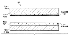
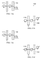
図1aおよび図1bは、SPGセルの形成プロセス100を示している。従来のLCセルを形成する際、LC配向層は、当該LCを挟み込むために使用される2枚の基板を被覆する2つのポリマー層をラビングまたは露光することにより形成される。SPGセルの形成プロセス100は、LC配向層を形成する工程に関して異なっている。SPGセルの形成プロセス100の第1の工程(図1a)では、2つの感光性ポリマー層102が2つのガラス基板106をそれぞれ被覆し、次いで、2枚のガラス基板を合体させて、LCを充填するためのギャップを残す。電極(導体)層104が更に、各感光性ポリマー層102と各感光性ポリマー層102に対応するガラス基板106との間に付加される。次に(図1b)、円偏光の回転方向が互いに反対である(それぞれ、右円偏光および左円偏光を有する)2つの干渉紫外(UV)光ビーム192が、(適切な入射角で)2つのポリマー層102を露光するのに用いられ(例えば、これらのガラス基板106を介して)、ホログラフィックパターンがこれらのポリマー層102に形成される。この干渉ビーム露光がSPGセルの各面に対して行われることで、配向層が感光性ポリマー層102から形成される。LC108がギャップに充填され、2枚のガラス基板の間に挟み込まれる場合、LC108の分子は、この段階でLC配向層として機能するこれらの感光性ポリマー層102の上に形成されたホログラムパターンと位置合わせされるように配向される。
1a and 1b show a
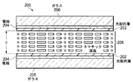
図2aおよび図2bはそれぞれ、電圧が印加されている状態および電圧が印加されていない状態のSPGセル200を示している。SPGセル200は、形成プロセス100を使用して形成することができる。電圧が電極層204に印加されていない状態(図2a)では、SPGセル200のLC208は回折格子を形成し、この回折格子によって、ガラス基板206のいずれの部分への入射光も、これらの配向層202を形成するための2本の露光ビームの角度で決まる方向(形成プロセス100中に決まる方向)に回折される。ゼロではない電圧がこれらの電極層204に電圧が印加されると(図2b)、LC208分子は、印加電圧によって生じる電界に位置合わせされるように配向するようになるので、LC回折格子の影響(配向層202によって生じる)が打ち消されてなくなり、ガラス基板206のいずれの部分への入射光も、回折されなくなる。LC回折格子の影響を打ち消すためには、十分大きな電圧が、例えば閾値電圧(Vth)を超える電圧が必要になる。
2a and 2b show the
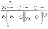
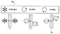
上に説明したSPGセルは、普通の回折格子とは異なる0次および±1次の3つの回折次数を有する。図3a〜図3cは、SPGセルのそれぞれ異なる動作モード300を示している。各動作モードは、1つの回折次数に対応し、各次数の光は、異なる角度に回折される。十分大きな電圧がSPGセルに印加されている状態(図3a)では、光は、入射光の偏光が如何なる状態であっても回折されて0次数光となる。電圧が印加されていない状態、または低い電圧が印加されている状態(図3bおよび図3c)では、回折光方向は、入射光の偏光によって異なる。右円偏光された入射光ビームは、回折されて+1次数光(図3a)となるのに対し、左円偏光された入射光ビームは、回折されて−1次数光(図3c)となる。SPGセルによって回折された後、光の円偏光が、図3bおよび図3cに示すように反転する(右円偏光と左円偏光との間で切り替わる)。
The SPG cell described above has three diffraction orders of 0th order and ± 1st order that are different from ordinary diffraction gratings. Figures 3a to 3c show
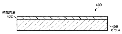
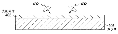
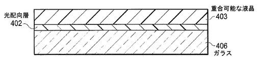
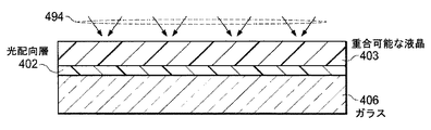
図4a〜図4dは、PPGセルの形成プロセス400を示している。PPGセルの形成プロセス400の第1の工程(図4a)では、光配向層402でガラス基板406を被覆する。第2の工程(図4b)では、ポリマー層402が、円偏光の回転方向が互いに反対である2つの干渉UVビーム(492)で露光される。第3の工程(図4c)では、重合性LC層403で光配向層402の上面を被覆する。第4の工程(図4d)では、均一なUVビーム494を用いて、重合性LC層403を照射して、当該層のLC組成物(分子)を重合させる。このようにして、ポリマー回折格子がガラス基板406に形成される。
4a-4d illustrate a
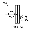
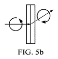
結果として得られるPPGセルは、当該PPGセルの回折特性を、電圧を印加することによって変化させる(上に説明したSPGセルの場合におけるように)ことができないという点で、特性が一定の回折格子である。図5aおよび図5bは、PPGセルの異なる動作モード500を示している。各動作モードは、1つの回折次数に対応し、各次数光は、異なる角度に回折される。入射光ビームは、2つの方向のうちの一方の方向に回折される。詳細には、右円偏光を有する入射光ビームは、回折されて+1次光(図5a)となるのに対し、左円偏光を有する入射光ビームは、回折されて−1次光(図5b)となる。いずれの場合においても、回折後、ビームの偏光の回転方向が、反対の回転方向に変化、すなわち切り替わる。
The resulting PPG cell is a diffraction grating with a constant characteristic in that the diffraction characteristic of the PPG cell cannot be changed by applying a voltage (as in the case of the SPG cell described above). It is. Figures 5a and 5b show
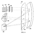
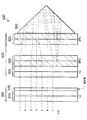
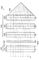
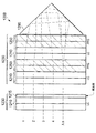
図6は、WSS(波長選択スイッチ)の具体的な光学系600を示している。WSS光学系600は、ファイバアレイ601と、マイクロレンズアレイ602と、ビーム偏向アレイ603と、1/2波長板アレイ604と、シリンドリカルレンズ605と、シリンドリカル反射ミラー606と、回折格子607と、光スイッチエンジン608とを含む。WSS光学系600のこれらの構成素子は、図6に示す通りに配置することができる、または同じ機能または同様の機能を実現する任意の他の適切な配置となるように配置することができる。他の実施形態では、上に説明した構成素子と同様であって良いし、または上に説明した構成素子とは異なる更に別の構成素子を用いることもできる。これらの構成素子のうちの幾つかの構成素子の代わりに、同じ機能を実現する同じ構成素子、または他の構成素子の組み合わせを用いることもできる。
FIG. 6 shows a specific
ファイバアレイ601は、入力ポートおよび出力ポートに使用される。1つのファイバ601からの入力光ビームまたは入射光ビームは、マイクロレンズアレイ602、ビーム偏向アレイ603、および1/2波長板アレイ604を通過すると、当該ビームは、同じ直線偏光を有する2本の平行ビームに分離される。次に、2本の光ビームは、シリンドリカルレンズ605およびシリンドリカル反射ミラー606を通過した後にコリメートされたビームになる。次に、これらの光ビームは、回折格子607によって回折されて、複数の波長に分離される。次いで、各波長光は、光スイッチエンジン608に集光される。光スイッチエンジン608は、各波長光を所定のポートにルーティングする。対応する光ビームは、光学系600を(複数の構成素子を逆の順番で)再び通過し、所定の出力ファイバに入射して結合される。
The
WSS光学系600の光スイッチエンジン608は、以下に説明するSPGセルおよびLCセルの複合素子、またはPPGセルおよびLCセルの複合素子を含む適切なWSS(波長選択スイッチ)システムを用いて実現することができる。使用されている他のWSS(波長選択スイッチ)技術(例えば、MEMS,LCOS,LC,ウェッジプレート、DMD)と比較すると、SPGまたはPPGを用いるWSSシステムは、光学系が単純である、電子駆動回路が簡単である、信頼性が高い、高性能である、多くのポート数を容易に実現できる、また製品コストを低く抑えることができるといった利点を有する。
The
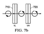
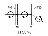
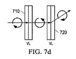
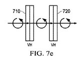
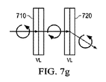
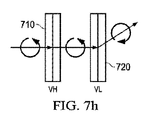
図7a〜図7hは、LCセルおよびSPGセルの複合素子のそれぞれ異なる動作モード700を示している。LCセル710は、SPGセル720の手前に配置される(入射光から見た場合)。LCセル710は、光の偏光を制御すなわち切り替えるのに用いられる。またSPGセル720は、光ビームを所定の方向に回折させるのに用いられる。
7a to 7h show
図7a,7c,7e,および図7hに示すように、比較的大きな電圧(VH)(例えば、閾値を上回る電圧)をLCセル710に印加すると、入射光ビームの偏光は、LCセルを通過しても変化しない。図7b,7d,7f,および図7gに示すように、電圧をLCセル710に印加しない状態、または比較的小さな電圧(VL)(例えば、閾値を下回る電圧)をLCセル710に印加した状態では、入射光ビームの偏光の回転方向が切り替わる。図7a,7b,7e,および図7fに示すように、比較的大きな電圧(VH)(例えば、閾値を上回る電圧)をSPGセル720に印加すると、入力光の偏光が如何なる状態であっても、光ビームは回折されて0次光となる。図7c,7d,7g、および図7hに示すように、電圧をSPGセル720に印加しない状態、または比較的小さな電圧(VL)(例えば、閾値を下回る電圧)をSPGセル720に印加した状態では、LCセル710によって制御される入射光の偏光によって異なるが、光ビームは、+1次光または−1次光のいずれかとなるように回折されうる。入力光が右円偏光または左円偏光であるか否かに関係なく、LCセル710およびSPGセル720の複合素子は、光ビームを3つの方向にルーティングして、1×3型光スイッチを形成する。N個のグループのLCセルおよびSPGセルは、1×3N型光スイッチを実現することができる。
As shown in FIGS. 7a, 7c, 7e, and 7h, when a relatively large voltage (VH) (eg, a voltage above a threshold) is applied to the
図8は、LCセルおよびSPGセルの複合素子を用いる具体的な光スイッチエンジン800の断面を示している。光スイッチエンジン800は、WSS光学系600の光スイッチエンジン608として使用することができる。光スイッチエンジン800は、偏光板815に接続されるLCセル810を含む可変光減衰器(VOA)805と、1/4波長板(QWP)840と、2つの連続するLCセル810およびSPGセル820からなる対を含む1×9型光スイッチ830と、プリズムまたはミラー890とを備える。これらの構成素子は、図8に示す通りに、または別の適切な順番で配置することができる。LCセル810およびSPGセル820は、M個の画素を、N=9本のビームと直交する方向(図8の紙面に垂直な方向)に有することができる。図8では、Nはポート数に対応するビームの本数であり、Mは波長チャネル数に対応する画素の個数である。光エンジン800に使用されるLCセルは、電気制御複屈折(ECB)セル、ツイステッドネマチック(TN)セル、および垂直配向(VA)セルであって良い。
FIG. 8 shows a cross section of a specific
簡潔性を期して、スイッチエンジンの動作原理は、図8のエンジン800の断面に図示されているように1つの波長について説明される。しかしながら、同じ動作原理は全てのM個の画素に適用される。
For the sake of brevity, the operating principle of the switch engine is described for one wavelength as illustrated in the cross section of the
入力光は最初に、光出力の減衰を制御するために使用されるVOA805を通過する。LCセル810に加わる電圧を制御することにより、VOA805の光出力量を制御することができる。QWP840を使用して、光の直線偏光を円偏光に変化させる。次に、光ビームは、2グループのLCセル810およびSPGセル820(1×9型光スイッチ830)を通過する。従って、出力ビームは、光軸に対して9通りの角度をとりうる。次に、当該ビームは、プリズムまたはミラー890で反射され、スイッチ830を通過した後に、光軸に平行になる。光スイッチエンジン800は、適正に設計されて、任意の2つの隣接光路(9通りの切り替え角度)間の距離をほぼ等しくすることができる。従って、基準ファイバアレイは、光出力ポート(例えば、9個の出力ポートを備える)として使用することができる。
The input light first passes through a
図9は、LCセルおよびSPGセルの複合素子を用いる具体的な別の光スイッチエンジン900の断面を示している。光スイッチエンジン900は、WSS光学系600の光スイッチエンジン608として使用することができる。光スイッチエンジン900は、偏光板915に接続されるLCセル910を含むVOA905と、1対のLCセル910およびSPGセル920、および後段の第2のSPGセル920を含む1×7型光スイッチ930と、プリズムまたはミラー890とを備える。これらの構成素子は、図9に示す通りに、または別の適切な順番で配置することができる。LCセル910およびSPGセル920は更に、M個の画素を、N=7本のビームと直交する方向(図9の紙面に垂直な方向)に有することができる。光スイッチエンジン900と光スイッチエンジン800との1つの違いは、光スイッチエンジン900が、1つのLCセル910および2つのSPGセル920を使用して、1×7型光スイッチを実現していることである。1×7型光スイッチでは、LCセル910を使用して、光の偏光を制御し、2つのSPGセル920を使用して、光を所定の角度に回折させる。更に、光スイッチエンジン900はQWPを含んでいない。その代わり、VOA905のLCセル910が、切り替え可能な1/4波長板(λ/4と3λ/4との間で切り替わる)として設計されて、入射光の直線偏光を円偏光に変化させる。光出力ポート数を増やすために、更に多くのSPGセル920を光スイッチエンジン900に、例えばミラーまたはプリズム990の前方に追加することができる。例えば、SPGセル920がN個の場合、1×(2N+1−1)型光スイッチエンジンが実装されて良い。
FIG. 9 shows a cross section of another specific
図10は、LCセルおよびSPGセルの複合素子を用いる具体的な更に別の光スイッチエンジン1000の断面を示している。光スイッチエンジン1000は、WSS光学系600の光スイッチエンジン608として使用することができる。光スイッチエンジン1000は、偏光板1015に接続されるLCセル1010を含むVOA1005と、QWP1040と、3つのSPGセル1020を含む1×8型光スイッチ1030と、プリズムまたはミラー1090とを備える。これらの構成素子は、図10に示す通りに、または別の適切な順番で配置することができる。これらのSPGセル1020は更に、M個の画素を、N=8本のビームと直交する方向(図10の紙面に垂直な方向)に有することができる。上に説明した光スイッチエンジン800および900とは異なり、光スイッチエンジン1000は、LCセルを用いることなくSPGセル群1020のみを使用して光回折角を制御する。光ビームがVOA1005およびQWP1040を通過した後、入力ビームの直線偏光は円偏光に変化する。各SPGセル1020は、光ビームを2通りの角度に回折させることができる。従って、SPGセルがN個ある場合、1×2N型光スイッチエンジンを形成することができる。
FIG. 10 shows a cross section of still another specific
図11a〜図11dは、LCセルおよびSPGセルの複合素子の異なる動作モード1100を示している。LCセル1110は、SPGセル1150の手前に配置される(入射光から見た場合)。LCセル1110を用いて、光の偏光を制御する、または切り替え、またPPGセル1150を用いて光ビームを、入力光の偏光によって異なるが、2通りの方向のうちの一方の方向に回折させる。従って、LCセルおよびPPGセルからなるN個の群は、1×2N型光スイッチを構成することができる。
Figures 11a to 11d show different modes of
図11aおよび図11dに示すように、VH(例えば、閾値を上回る電圧)をLCセル1110に印加すると、入射光ビームの偏光は、LCセルを通過することにより変化することはない。図11bおよび図11cに示すように、電圧をLCセル1110に印加しない状態、またはVL(例えば、閾値を下回る電圧)をLCセル1110に印加した状態では、入射光ビームの偏光の左右が切り替わる。図11aおよび図11cに示すように、PPGセル1150への入射光が、右円偏光を有する場合、光ビームは回折されて+1次数光となる。図11bおよび図11dに示すように、PPGセル1150への入射光が、左円偏光されている場合、光ビームは回折されて−1次数光となる。
As shown in FIGS. 11a and 11d, when VH (eg, a voltage above a threshold) is applied to the
図12は、LCセルおよびSPGセルの複合素子を用いる具体的な光スイッチエンジン1200の断面を示している。光スイッチエンジン1200は、WSS光学系600の光スイッチエンジン608として使用することができる。光スイッチエンジン1200は、偏光板1215に接続されるLCセル1210を含むVOA1205と、2つの連続するLCセル1210およびPPGセル1250からなる対を含む1×4型光スイッチ1230と、プリズムまたはミラー1290とを備える。これらの構成素子は、図12に示す通りに、または別の適切な順番で配置することができる。これらのLCセル1210およびPPGセル1250は、M個の画素を、N=4本のビームと直交する方向(図12の紙面に垂直な方向)に有することができる。同様の光スイッチは、必要数のLCおよびPPGペアを積層して合体させることにより、任意の数の出力ポートを有するように設計することができる。
FIG. 12 shows a cross section of a specific
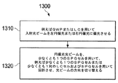
図13は、光スイッチエンジンを、LCセルおよびSPGセルを用いて動作させる具体的な方法1300を示している。例えば、方法1300は、光スイッチエンジン800,900,および1000のうちのいずれかの光スイッチエンジンを用いて実施される。工程1310では、入射光ビームを、左円偏光または右円偏光に偏光させる。例えば、QWP840または1040、或いは電気的に切り替え可能な(電圧を印加することにより)LCを用いて、直線偏光する入射光ビームを円偏光する光に変換する。工程1320では、円偏光する光ビームが、少なくとも1つのSPGセルを用いて回折される。回折光ビームの偏光の回転方向が更に切り替えられる。例えば、円偏光する光が、左回り方向と右回り方向との間で、1×9型光スイッチ830の電気的に切り替え可能な第1のLC810(または、1×7型光スイッチ930のLC910)を用いて切り替えられ、続いて、電気的に切り替え可能な次段のSPG820(または、920)により、対応する角度に回折される。別の例では、円偏光する光が、1×8型光スイッチ1030の電気的に切り替え可能な第1のSPG1020により、対応する角度に直接回折される。
FIG. 13 shows a
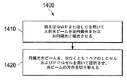
図14は、LCセルおよびPPGセルを用いて光スイッチエンジンを動作させる具体的な方法1400を示している。例えば、方法1400は、光スイッチエンジン1200を用いて実施される。工程1410では、入射光ビームが、左円偏光または右円偏光に偏光される。例えば、電気的に切り替え可能なLCを用いて、直線偏光する入射光ビームが円偏光する光に変換される。工程1420では、円偏光する光ビームが、少なくとも1対のLCセルおよびPPGセルを用いて回折される。回折光ビームの偏光の回転方向が更に切り替えられる。例えば、円偏光光は、左回り方向と右回り方向との間で、1×4型光スイッチ1230の電気的に切り替え可能な第1のLC1210を用いて切り替えられ、続いて、電気的に切り替え可能な次段のSPG1250により、対応する角度に回折される。
FIG. 14 shows a
本発明について、例示的な実施形態を参照して説明してきたが、この説明は、限定的な意味に解釈されてはならない。例示の実施形態の種々の変形および組み合わせ、ならびに本発明の他の実施形態は、当業者には、説明を参照することにより明らかになる。従って、添付の請求項は、このような変形または実施形態の全てを包含する。 Although the present invention has been described with reference to illustrative embodiments, this description should not be construed in a limiting sense. Various modifications and combinations of the exemplary embodiments, as well as other embodiments of the invention, will be apparent to persons skilled in the art upon reference to the description. Accordingly, the appended claims encompass all such variations or embodiments.
本発明は、光スイッチに関するものであり、特に波長を選択的に切り替える装置および方法に関するものである。 The present invention relates to an optical switch, and more particularly to an apparatus and method for selectively switching wavelengths.
光伝送ネットワーク機器の場合、再構築可能な光挿入/分岐マルチプレクサ(ROADM)を使用すると、ネットワーク能力を柔軟に拡張することができ、運用コストを低減することができる。波長選択スイッチ(WSS)は、現在のROADM技術を用いる場合の1つの選択肢である。1×N型WSS(波長選択スイッチ)の場合、1は共通(COM)ポートであり、Nは分岐ポート数を表している。WSS(波長選択スイッチ)が動作すると、WDM信号群がCOMポートから入力されると、これらの信号は光波長ごとに分離され、次いで、システム要件に従って、各波長はN個の分岐ポートのうちの1つの分岐ポートにルーティングされる。逆に、これらの光信号は、N個の分岐ポートからの入力として受信することができ、COMポートからの出力として送信することができる。 In the case of optical transmission network equipment, the use of a reconfigurable optical add / drop multiplexer (ROADM) can flexibly expand network capabilities and reduce operating costs. A wavelength selective switch (WSS) is one option when using current ROADM technology. In the case of a 1 × N type WSS (wavelength selective switch), 1 is a common (COM) port, and N represents the number of branch ports. When WSS (Wavelength Selective Switch) operates, when a group of WDM signals are input from the COM port, these signals are separated for each optical wavelength, and then each wavelength is one of N branch ports according to the system requirements. Routed to one branch port. Conversely, these optical signals can be received as inputs from N branch ports and transmitted as outputs from COM ports.
ROADMは、コストが高く付き、かつサービスを中断する「フォークリフト)」アップグレードに頼ることなく、容量を必要に応じて柔軟に増加させる自動機構を提供する。ROADMネットワークの利点は、ROADMネットワークが、必要なときにどの場所でも、かつ如何なるときでも、下層ネットワークが、増大したトラフィックを自動的に補償する状態を確保しながら、容量を動的に増加させることができることである。これにより、手動調整または大規模なアップグレードが不要となる。ROADMは、挿入/分岐機能を複数の方向に複数の波長チャネルについて提供することができるので、ネットワークリング群間の多方向相互接続を実現し、メッシュ型ネットワークを構築するのに適している。 ROADM provides an automated mechanism that flexibly increases capacity as needed, without resorting to “forklift” upgrades that are costly and interrupt service. The advantage of a ROADM network is that the ROADM network dynamically increases capacity while ensuring that the underlying network automatically compensates for increased traffic wherever and whenever it is needed. It is possible to do. This eliminates the need for manual adjustments or large scale upgrades. ROADM can provide insertion / branching functions for a plurality of wavelength channels in a plurality of directions, and thus is suitable for realizing a multi-directional interconnection between network ring groups and constructing a mesh network.
1つの実施形態によれば、光スイッチは、液晶セルと、前記液晶セルに隣接する切り替え可能な偏光回折格子(SPG)セルとを含む。前記SPGは、第1のガラス基板と、前記第1のガラス基板を覆う第1の電極層と、前記第1の電極層を覆う光配向層と、前記光配向層を覆う液晶材料と、前記液晶材料を覆う第2の光配向層とを含む。前記第1の光配向層および前記第2の光配向層は、円偏光の回転方向が互いに反対である2つの干渉光ビームを使用して露光されることにより物理的に変化した感光性ポリマーを含む。前記SPGは更に、前記第2の光配向層を覆う第2の電極層と、前記第2の電極層を覆う第2のガラス基板とを含む。 According to one embodiment, the optical switch includes a liquid crystal cell and a switchable polarization grating (SPG) cell adjacent to the liquid crystal cell. The SPG includes a first glass substrate, a first electrode layer that covers the first glass substrate, a photo-alignment layer that covers the first electrode layer, a liquid crystal material that covers the photo-alignment layer, A second photo-alignment layer covering the liquid crystal material. The first photo-alignment layer and the second photo-alignment layer may be formed of a photosensitive polymer that has been physically changed by being exposed using two interference light beams whose rotation directions of circularly polarized light are opposite to each other. Including. The SPG further includes a second electrode layer that covers the second photo-alignment layer, and a second glass substrate that covers the second electrode layer.
別の実施形態によれば、光スイッチは、液晶セルと、前記液晶セルに隣接するポリマー液晶偏光回折格子(PPG)セルとを含む。前記PPGは、ガラス基板と、前記ガラス基板を覆い、かつ円偏光の回転方向が互いに反対である2つの干渉光ビームを使用して露光されることにより物理的に変化している感光性ポリマーを含む光配向層と、前記光配向層を前記ガラス基板の反対側で覆い、かつ均一光ビームを用いる照射により物理的に変化した重合液晶層とを含む。 According to another embodiment, the optical switch includes a liquid crystal cell and a polymer liquid crystal polarization grating (PPG) cell adjacent to the liquid crystal cell. The PPG comprises a glass substrate and a photosensitive polymer that is physically changed by being exposed using two interference light beams that cover the glass substrate and have opposite directions of rotation of circularly polarized light. And a polymerized liquid crystal layer that covers the photo-alignment layer on the opposite side of the glass substrate and is physically changed by irradiation using a uniform light beam.
更に別の実施形態によれば、偏光回折格子を含む光スイッチを動作させる方法は、入射光ビームを円偏光に偏光させる工程と、前記偏光光ビームを前記偏光回折格子に誘導する工程と、前記偏光回折格子で、前記偏光入射光ビームを、前記入射光ビームの前記円偏光に応じた回折次数及び2つの干渉光ビームを用いて形成される、前記偏光回折格子の内部に形成されるホログラムパターン方向に対応する所定の角度で、回折させる工程とを含む。 According to yet another embodiment, a method of operating an optical switch that includes a polarization grating comprises: polarizing an incident light beam into circularly polarized light; directing the polarized light beam to the polarization diffraction grating; A hologram pattern formed in the polarization diffraction grating, wherein the polarization incident light beam is formed using a diffraction order corresponding to the circularly polarized light of the incident light beam and two interference light beams. Diffracting at a predetermined angle corresponding to the direction.
本発明および本発明の利点を更に完全に理解するために、次に以下の説明を添付の図面と併せて参照する。 For a more complete understanding of the present invention and the advantages thereof, reference is now made to the following description, taken in conjunction with the accompanying drawings, in which:
現時点で好適な実施形態を構成し、使用する手法について以下に詳細に説明する。しかしながら、本発明は、非常に多岐に亘る特定の状況で具体化することができる多くの適用可能な革新的なコンセプトを提供することを理解されたい。説明する特定の実施形態は、本発明を構成し、使用するための特定のやり方を単に例示しているに過ぎず、本発明の範囲を限定するものではない。 The method of configuring and using the presently preferred embodiment is described in detail below. However, it should be understood that the present invention provides many applicable innovative concepts that can be implemented in a very wide variety of specific situations. The particular embodiments described are merely illustrative of specific ways to make and use the invention, and do not limit the scope of the invention.
波長選択スイッチ(WSS)製品に現在使用されている技術として、微小電気機械システム(MEMS)、液晶オンシリコン(LCOS)、くさび型結晶を備える液晶(LC)、およびデジタルマイクロミラー素子(DMD)を挙げることができる。これらの技術の場合、これらの光学系は、光スイッチエンジンが異なる以外は、互いに同様とすることができる。 Technologies currently used in wavelength selective switch (WSS) products include microelectromechanical systems (MEMS), liquid crystal on silicon (LCOS), liquid crystals with wedge crystals (LC), and digital micromirror devices (DMD) Can be mentioned. For these technologies, these optical systems can be similar to each other, except for the optical switch engine.
MEMS(微小電気機械システム)では、これらの波長は、回折格子によりそれぞれ異なるチャネルへ向かうように回折されて、次いで、各波長は、対応するMEMS反射ミラーに入射する。各MEMS反射ミラーに加わる電圧を制御することにより、ミラーの回転角を制御して、光反射角を制御することができる。ネットワークの要件に従って、各波長を所定の角度に反射することができる。複数のチャネルから同じ角度に反射される波長ビームは、回折格子を2回目に通過した後に、回折されて1つのビームになることができ、次いで、出力ポートへ入射して結合することができる。切り替え時に光減衰量を制御し、かつヒットレス機能を実現するために、各MEMSミラーは、2つの回転方向を有し、一の回転でポート切り替えを行い、他の回転で減衰量およびヒットレス機能を制御する。MEMS系WSSは、光学系が単純であり、性能が良好であるという利点を有する。しかしながら、MEMS系WSSは、比較的低い歩留まりに起因するMEMSチップ形成に要する高コスト、MEMSミラーに対する高電圧駆動要件に起因する電子素子に要する高コスト、非常に多くのポートを実現する難しさ、および柔軟なグリッド(Flexgrid)機能を設計する難しさといった幾つかの不具合を有する。 In MEMS (microelectromechanical system), these wavelengths are diffracted by the diffraction grating toward different channels, and then each wavelength is incident on a corresponding MEMS reflection mirror. By controlling the voltage applied to each MEMS reflection mirror, the rotation angle of the mirror can be controlled to control the light reflection angle. Each wavelength can be reflected at a predetermined angle according to network requirements. Wavelength beams reflected from multiple channels at the same angle can pass through the diffraction grating a second time before being diffracted into a single beam that can then enter the output port and combine. In order to control the optical attenuation at the time of switching and to realize the hitless function, each MEMS mirror has two rotation directions, the port is switched by one rotation, and the attenuation and hitless by the other rotation. Control the function. The MEMS system WSS has an advantage that the optical system is simple and the performance is good. However, the MEMS-based WSS has a high cost required for forming a MEMS chip due to a relatively low yield, a high cost required for an electronic device due to a high voltage driving requirement for the MEMS mirror, and a difficulty in realizing a very large number of ports. And has some deficiencies such as difficulty in designing a flexible grid function.
LCOSは、WSS(波長選択スイッチ)システムに使用される別の技術である。LCOSは、ガラス基板とシリコン背面との間に配置されるLC層から成る。LCOS系WSSでは、回折格子により分離される各波長光は、M×N画素を網羅するLCOSパネルに入射する。これらの画素に加わる電圧を制御することにより、入射光ビームが所定の角度に回折されるようなLC(液晶)位相回折格子を形成することができる。LC(液晶)回折格子ピッチを変えることにより、異なる回折角度が得られる。従って、ある波長光についてLC(液晶)位相回折格子ピッチを制御することにより、光ビームを所定の出力ポートにルーティングすることができる。LCOS系WSSは、光学系が単純である、多くのポート数が容易に実現される、柔軟なグリッド機能が容易に実現されるといった幾つかの利点を有する。不具合としては、電子駆動方式が複雑であること、制御ソフトウェアが極めて複雑であること、低クロストークを実現することが困難であること、および温度に対する感度が非常に高いことを挙げることができる。 LCOS is another technology used in WSS (wavelength selective switch) systems. LCOS consists of an LC layer placed between a glass substrate and a silicon backside. In the LCOS system WSS, each wavelength light separated by the diffraction grating is incident on an LCOS panel covering M × N pixels . By controlling the voltage applied to these pixels, an LC (liquid crystal) phase diffraction grating that diffracts the incident light beam at a predetermined angle can be formed. Different diffraction angles are obtained by changing the LC (liquid crystal) diffraction grating pitch. Therefore, by controlling the LC (liquid crystal) phase diffraction grating pitch for a certain wavelength light, the light beam can be routed to a predetermined output port. The LCOS-based WSS has several advantages such as a simple optical system, a large number of ports can be easily realized, and a flexible grid function can be easily realized. Problems include that the electronic drive system is complicated, the control software is extremely complex, it is difficult to achieve low crosstalk, and the sensitivity to temperature is very high.
WSS(波長選択スイッチ)に使用される別の技術が、結晶ウェッジを備えるLCである。結晶ウェッジを備えるLCを用いたWSS設計は、2009年3月3日に発行され、「Apparatus And Method for Optical Switching with Liquid Crystals And Birefringent Wedges(液晶および複屈折結晶ウェッジを用いた光スイッチング装置および方法)」と題する米国特許第7,499,608号明細書に記載されている。このようなWSSのスイッチエンジンは、出力ポートの必要数によって異なるが、数段のLCセルおよびウェッジプレート複合素子から成る。各段では、LCセルは、偏光を切り替えるのに使用され、またウェッジプレートは、光を、入射光の偏光によって異なるように2つの方向に屈折させるのに用いられる。その結果、1×2型光スイッチが得られる。従って、N段を積層すると、1×2N型光スイッチが得られる。使用するLCセルは、必要な光チャネル数によって定義されるM個の画素に分離される。LC画素に印加される電圧を制御することにより、対応する波長光を所定の出力ポート群にルーティングすることができる。このようなWSSは、駆動用電子素子が簡単であり、高い耐振動性を示し、高い信頼性を示すという利点を有する。不具合として、高い材料コストに起因する高コスト、複雑な素子組み立てプロセスに起因する比較的低い歩留まり、および非常に多いポート数を実現する難しさを挙げることができる。 Another technique used for WSS (wavelength selective switch) is LC with a crystal wedge. A WSS design using LC with a crystal wedge was published on March 3, 2009, "Apparatus And Method for Optical Switching with Liquids And Birefringent Wedges (Liquid Crystal and Birefringent Crystal Wedge Method Using Liquid Crystal and Birefringent Crystal Wedge Method) U.S. Pat. No. 7,499,608, entitled “)”. Such a WSS switch engine is composed of several stages of LC cells and wedge plate composite elements, depending on the required number of output ports. At each stage, the LC cell is used to switch the polarization, and the wedge plate is used to refract the light in two directions, depending on the polarization of the incident light. As a result, a 1 × 2 type optical switch is obtained. Therefore, when N stages are stacked, a 1 × 2 N- type optical switch is obtained. The LC cell used is separated into M pixels defined by the required number of optical channels. By controlling the voltage applied to the LC pixel, the corresponding wavelength light can be routed to a predetermined output port group. Such WSS has the advantage that the driving electronic element is simple, exhibits high vibration resistance, and exhibits high reliability. Problems include high cost due to high material costs, relatively low yield due to complex device assembly processes, and difficulty in achieving very large numbers of ports.
DMD(デジタルマイクロミラー素子)技術も、WSSシステムに使用される。このようなシステムでは、各波長光は、幾つかのDMD/MEMSミラーに入射する。これらのミラーの回転角を制御することにより、光ビームを所定の角度に誘導することができる。これらのミラーは、2つしか偏向位置を有しないので、1つのDMDチップ系WSSは、1×2型スイッチしか実現できない。WSSのスイッチポート数を増やすためには、より多くのDMDチップが必要になり、光学系設計が高コストになり、かつ非常に難しくなる。 DMD (digital micromirror device) technology is also used in WSS systems. In such a system, each wavelength light is incident on several DMD / MEMS mirrors. By controlling the rotation angle of these mirrors, the light beam can be guided to a predetermined angle. Since these mirrors have only two deflection positions, one DMD chip system WSS can implement only a 1 × 2 type switch. In order to increase the number of WSS switch ports, more DMD chips are required, and the optical system design becomes expensive and very difficult.
上に説明したように、既存の技術を用いるWSSシステムは、駆動用電子素子が複雑なソフトウェアを備えること、材料が高コストであること、振動耐性が低いこと、および非常に多くのポートに拡張することが困難であることを含む不具合を有している。本明細書において記載されるのは、WSS(波長選択スイッチ)を実現する具体的なシステムおよび方法である。異なる実施形態では、切り替え可能な偏光回折格子(SPG)セルおよびLCセルの複合素子、ならびにポリマー液晶偏光回折格子(PPG)セルおよびLCセルの複合素子を用いて、上に挙げたシステムの不具合のうちの少なくとも幾つかの不具合を解決する1×N型WSSシステムを実現する。 As explained above, WSS systems using existing technology, the drive electronics have complex software, the material is expensive, the vibration resistance is low, and it expands to a very large number of ports It has inconveniences including difficult to do. Described herein are specific systems and methods for implementing WSS (Wavelength Selective Switch). In a different embodiment, a switchable polarization grating (SPG) cell and LC cell composite element, and a polymer liquid crystal polarization grating (PPG) cell and LC cell composite element are used to address the above mentioned system failures. A 1 × N type WSS system that solves at least some of the problems is realized.
図1aおよび図1bは、SPGセルの形成プロセス100を示している。従来のLCセルを形成する際、LC配向層は、当該LCを挟み込むために使用される2枚の基板上に堆積される2つのポリマー層をラビングまたは露光することにより形成される。SPGセルの形成プロセス100は、LC配向層を形成する工程に関して異なっている。SPGセルの形成プロセス100の第1の工程(図1a)では、2つの感光性ポリマー層102が2つのガラス基板106上にそれぞれ堆積され、次いで、2枚のガラス基板を合体させて、LCを充填するためのギャップを残す。電極(導体)層104が更に、各感光性ポリマー層102と各感光性ポリマー層102に対応するガラス基板106との間に付加される。次に(図1b)、円偏光の回転方向が互いに反対である(それぞれ、右円偏光および左円偏光を有する)2つの干渉紫外(UV)光ビーム192が、(適切な入射角で)2つのポリマー層102を露光するのに用いられ(例えば、これらのガラス基板106を介して)、ホログラフィックパターンがこれらのポリマー層102に形成される。この干渉ビーム露光がSPGセルの各面に対して行われることで、配向層が感光性ポリマー層102から形成される。LC108がギャップに充填され、2枚のガラス基板の間に挟み込まれる場合、LC108の分子は、この段階でLC配向層として機能するこれらの感光性ポリマー層102の上に形成されたホログラムパターンと位置合わせされるように配向される。
1a and 1b show a
図2aおよび図2bはそれぞれ、電圧が印加されている状態および電圧が印加されていない状態のSPGセル200を示している。SPGセル200は、形成プロセス100を使用して形成することができる。電圧が電極層204に印加されていない状態(図2a)では、SPGセル200のLC208は回折格子を形成し、この回折格子によって、ガラス基板206のいずれの部分への入射光も、これらの配向層202を形成するための2本の露光ビームの角度で決まる方向(形成プロセス100中に決まる方向)に回折される。ゼロではない電圧がこれらの電極層204に電圧が印加されると(図2b)、LC208分子は、印加電圧によって生じる電界に位置合わせされるように配向するようになるので、LC回折格子の影響(配向層202によって生じる)が打ち消されてなくなり、ガラス基板206のいずれの部分への入射光も、回折されなくなる。LC回折格子の影響を打ち消すためには、十分大きな電圧が、例えば閾値電圧(Vth)を超える電圧が必要になる。
2a and 2b show the
上に説明したSPGセルは、普通の回折格子とは異なる0次および±1次の3つの回折次数を有する。図3a〜図3cは、SPGセルのそれぞれ異なる動作モード300を示している。各動作モードは、1つの回折次数に対応し、各次数の光は、異なる角度に回折される。十分大きな電圧がSPGセルに印加されている状態(図3a)では、光は、入射光の偏光が如何なる状態であっても回折されて0次数光となる。電圧が印加されていない状態、または低い電圧が印加されている状態(図3bおよび図3c)では、回折光方向は、入射光の偏光によって異なる。右円偏光された入射光ビームは、回折されて+1次数光(図3a)となるのに対し、左円偏光された入射光ビームは、回折されて−1次数光(図3c)となる。SPGセルによって回折された後、光の円偏光が、図3bおよび図3cに示すように反転する(右円偏光と左円偏光との間で切り替わる)。
The SPG cell described above has three diffraction orders of 0th order and ± 1st order that are different from ordinary diffraction gratings. Figures 3a to 3c show
図4a〜図4dは、PPGセルの形成プロセス400を示している。PPGセルの形成プロセス400の第1の工程(図4a)では、光配向層402がガラス基板406上に堆積される。第2の工程(図4b)では、ポリマー層402が、円偏光の回転方向が互いに反対である2つの干渉UVビーム(492)で露光される。第3の工程(図4c)では、重合性LC層403が光配向層402の上面に堆積される。第4の工程(図4d)では、均一なUVビーム494を用いて、重合性LC層403を照射して、当該層のLC組成物(分子)を重合させる。このようにして、ポリマー回折格子がガラス基板406に形成される。
4a-4d illustrate a
結果として得られるPPGセルは、当該PPGセルの回折特性を、電圧を印加することによって変化させる(上に説明したSPGセルの場合におけるように)ことができないという点で、特性が一定の回折格子である。図5aおよび図5bは、PPGセルの異なる動作モード500を示している。各動作モードは、1つの回折次数に対応し、各次数光は、異なる角度に回折される。入射光ビームは、2つの方向のうちの一方の方向に回折される。詳細には、右円偏光を有する入射光ビームは、回折されて+1次光(図5a)となるのに対し、左円偏光を有する入射光ビームは、回折されて−1次光(図5b)となる。いずれの場合においても、回折後、ビームの偏光の回転方向が、反対の回転方向に変化、すなわち切り替わる。
The resulting PPG cell is a diffraction grating with a constant characteristic in that the diffraction characteristic of the PPG cell cannot be changed by applying a voltage (as in the case of the SPG cell described above). It is. Figures 5a and 5b show
図6は、WSS(波長選択スイッチ)の具体的な光学系600を示している。WSS光学系600は、ファイバアレイ601と、マイクロレンズアレイ602と、ビーム偏向アレイ603と、1/2波長板アレイ604と、シリンドリカルレンズ605と、シリンドリカル反射ミラー606と、回折格子607と、光スイッチエンジン608とを含む。WSS光学系600のこれらの構成素子は、図6に示す通りに配置することができる、または同じ機能または同様の機能を実現する任意の他の適切な配置となるように配置することができる。他の実施形態では、上に説明した構成素子と同様であって良いし、または上に説明した構成素子とは異なる更に別の構成素子を用いることもできる。これらの構成素子のうちの幾つかの構成素子の代わりに、同じ機能を実現する同じ構成素子、または他の構成素子の組み合わせを用いることもできる。
FIG. 6 shows a specific
ファイバアレイ601は、入力ポートおよび出力ポートに使用される。1つのファイバ601からの入力光ビームまたは入射光ビームは、マイクロレンズアレイ602、ビーム偏向アレイ603、および1/2波長板アレイ604を通過すると、当該ビームは、同じ直線偏光を有する2本の平行ビームに分離される。次に、2本の光ビームは、シリンドリカルレンズ605およびシリンドリカル反射ミラー606を通過した後にコリメートされたビームになる。次に、これらの光ビームは、回折格子607によって回折されて、複数の波長に分離される。次いで、各波長光は、光スイッチエンジン608に集光される。光スイッチエンジン608は、各波長光を所定のポートにルーティングする。対応する光ビームは、光学系600を(複数の構成素子を逆の順番で)再び通過し、所定の出力ファイバに入射して結合される。
The
WSS光学系600の光スイッチエンジン608は、以下に説明するSPGセルおよびLCセルの複合素子、またはPPGセルおよびLCセルの複合素子を含む適切なWSS(波長選択スイッチ)システムを用いて実現することができる。使用されている他のWSS(波長選択スイッチ)技術(例えば、MEMS,LCOS,LC,ウェッジプレート、DMD)と比較すると、SPGまたはPPGを用いるWSSシステムは、光学系が単純である、電子駆動回路が簡単である、信頼性が高い、高性能である、多くのポート数を容易に実現できる、また製品コストを低く抑えることができるといった利点を有する。
The
図7a〜図7hは、LCセルおよびSPGセルの複合素子のそれぞれ異なる動作モード700を示している。LCセル710は、SPGセル720の手前に配置される(入射光から見た場合)。LCセル710は、光の偏光を制御すなわち切り替えるのに用いられる。またSPGセル720は、光ビームを所定の方向に回折させるのに用いられる。
7a to 7h show
図7a,7c,7e,および図7hに示すように、比較的大きな電圧(VH)(例えば、閾値を上回る電圧)をLCセル710に印加すると、入射光ビームの偏光は、LCセルを通過しても変化しない。図7b,7d,7f,および図7gに示すように、電圧をLCセル710に印加しない状態、または比較的小さな電圧(VL)(例えば、閾値を下回る電圧)をLCセル710に印加した状態では、入射光ビームの偏光の回転方向が切り替わる。図7a,7b,7e,および図7fに示すように、比較的大きな電圧(VH)(例えば、閾値を上回る電圧)をSPGセル720に印加すると、入力光の偏光が如何なる状態であっても、光ビームは回折されて0次光となる。図7c,7d,7g、および図7hに示すように、電圧をSPGセル720に印加しない状態、または比較的小さな電圧(VL)(例えば、閾値を下回る電圧)をSPGセル720に印加した状態では、LCセル710によって制御される入射光の偏光によって異なるが、光ビームは、+1次光または−1次光のいずれかとなるように回折されうる。入力光が右円偏光または左円偏光であるか否かに関係なく、LCセル710およびSPGセル720の複合素子は、光ビームを3つの方向にルーティングして、1×3型光スイッチを形成する。N個のグループのLCセルおよびSPGセルは、1×3N型光スイッチを実現することができる。
As shown in FIGS. 7a, 7c, 7e, and 7h, when a relatively large voltage (VH) (eg, a voltage above a threshold) is applied to the
図8は、LCセルおよびSPGセルの複合素子を用いる具体的な光スイッチエンジン800の断面を示している。光スイッチエンジン800は、WSS光学系600の光スイッチエンジン608として使用することができる。光スイッチエンジン800は、偏光板815に接続されるLCセル810を含む可変光減衰器(VOA)805と、1/4波長板(QWP)840と、2つの連続するLCセル810およびSPGセル820からなる対を含む1×9型光スイッチ830と、プリズムまたはミラー890とを備える。これらの構成素子は、図8に示す通りに、または別の適切な順番で配置することができる。LCセル810およびSPGセル820は、M個の画素を、N=9本のビームと直交する方向(図8の紙面に垂直な方向)に有することができる。図8では、Nはポート数に対応するビームの本数であり、Mは波長チャネル数に対応する画素の個数である。光エンジン800に使用されるLCセルは、電気制御複屈折(ECB)セル、ツイステッドネマチック(TN)セル、および垂直配向(VA)セルであって良い。
FIG. 8 shows a cross section of a specific
簡潔性を期して、スイッチエンジンの動作原理は、図8のエンジン800の断面に図示されているように1つの波長について説明される。しかしながら、同じ動作原理は全てのM個の画素に適用される。
For the sake of brevity, the operating principle of the switch engine is described for one wavelength as illustrated in the cross section of the
入力光は最初に、光出力の減衰を制御するために使用されるVOA805を通過する。LCセル810に加わる電圧を制御することにより、VOA805の光出力量を制御することができる。QWP840を使用して、光の直線偏光を円偏光に変化させる。次に、光ビームは、2グループのLCセル810およびSPGセル820(1×9型光スイッチ830)を通過する。従って、出力ビームは、光軸に対して9通りの角度をとりうる。次に、当該ビームは、プリズムまたはミラー890で反射され、スイッチ830を通過した後に、光軸に平行になる。光スイッチエンジン800は、適正に設計されて、任意の2つの隣接光路(9通りの切り替え角度)間の距離をほぼ等しくすることができる。従って、基準ファイバアレイは、光出力ポート(例えば、9個の出力ポートを備える)として使用することができる。
The input light first passes through a
図9は、LCセルおよびSPGセルの複合素子を用いる具体的な別の光スイッチエンジン900の断面を示している。光スイッチエンジン900は、WSS光学系600の光スイッチエンジン608として使用することができる。光スイッチエンジン900は、偏光板915に接続されるLCセル910を含むVOA905と、1対のLCセル910およびSPGセル920、および後段の第2のSPGセル920を含む1×7型光スイッチ930と、プリズムまたはミラー890とを備える。これらの構成素子は、図9に示す通りに、または別の適切な順番で配置することができる。LCセル910およびSPGセル920は更に、M個の画素を、N=7本のビームと直交する方向(図9の紙面に垂直な方向)に有することができる。光スイッチエンジン900と光スイッチエンジン800との1つの違いは、光スイッチエンジン900が、1つのLCセル910および2つのSPGセル920を使用して、1×7型光スイッチを実現していることである。1×7型光スイッチでは、LCセル910を使用して、光の偏光を制御し、2つのSPGセル920を使用して、光を所定の角度に回折させる。更に、光スイッチエンジン900はQWPを含んでいない。その代わり、VOA905のLCセル910が、切り替え可能な1/4波長板(λ/4と3λ/4との間で切り替わる)として設計されて、入射光の直線偏光を円偏光に変化させる。光出力ポート数を増やすために、更に多くのSPGセル920を光スイッチエンジン900に、例えばミラーまたはプリズム990の前方に追加することができる。例えば、SPGセル920がN個の場合、1×(2N+1−1)型光スイッチエンジンが実装されて良い。
FIG. 9 shows a cross section of another specific
図10は、LCセルおよびSPGセルの複合素子を用いる具体的な更に別の光スイッチエンジン1000の断面を示している。光スイッチエンジン1000は、WSS光学系600の光スイッチエンジン608として使用することができる。光スイッチエンジン1000は、偏光板1015に接続されるLCセル1010を含むVOA1005と、QWP1040と、3つのSPGセル1020を含む1×8型光スイッチ1030と、プリズムまたはミラー1090とを備える。これらの構成素子は、図10に示す通りに、または別の適切な順番で配置することができる。これらのSPGセル1020は更に、M個の画素を、N=8本のビームと直交する方向(図10の紙面に垂直な方向)に有することができる。上に説明した光スイッチエンジン800および900とは異なり、光スイッチエンジン1000は、LCセルを用いることなくSPGセル群1020のみを使用して光回折角を制御する。光ビームがVOA1005およびQWP1040を通過した後、入力ビームの直線偏光は円偏光に変化する。各SPGセル1020は、光ビームを2通りの角度に回折させることができる。従って、SPGセルがN個ある場合、1×2N型光スイッチエンジンを形成することができる。
FIG. 10 shows a cross section of still another specific
図11a〜図11dは、LCセルおよびSPGセルの複合素子の異なる動作モード1100を示している。LCセル1110は、SPGセル1150の手前に配置される(入射光から見た場合)。LCセル1110を用いて、光の偏光を制御する、または切り替え、またPPGセル1150を用いて光ビームを、入力光の偏光によって異なるが、2通りの方向のうちの一方の方向に回折させる。従って、LCセルおよびPPGセルからなるN個の群は、1×2N型光スイッチを構成することができる。
Figures 11a to 11d show different modes of
図11aおよび図11dに示すように、VH(例えば、閾値を上回る電圧)をLCセル1110に印加すると、入射光ビームの偏光は、LCセルを通過することにより変化することはない。図11bおよび図11cに示すように、電圧をLCセル1110に印加しない状態、またはVL(例えば、閾値を下回る電圧)をLCセル1110に印加した状態では、入射光ビームの偏光の左右が切り替わる。図11aおよび図11cに示すように、PPGセル1150への入射光が、右円偏光を有する場合、光ビームは回折されて+1次数光となる。図11bおよび図11dに示すように、PPGセル1150への入射光が、左円偏光されている場合、光ビームは回折されて−1次数光となる。
As shown in FIGS. 11a and 11d, when VH (eg, a voltage above a threshold) is applied to the
図12は、LCセルおよびSPGセルの複合素子を用いる具体的な光スイッチエンジン1200の断面を示している。光スイッチエンジン1200は、WSS光学系600の光スイッチエンジン608として使用することができる。光スイッチエンジン1200は、偏光板1215に接続されるLCセル1210を含むVOA1205と、2つの連続するLCセル1210およびPPGセル1250からなる対を含む1×4型光スイッチ1230と、プリズムまたはミラー1290とを備える。これらの構成素子は、図12に示す通りに、または別の適切な順番で配置することができる。これらのLCセル1210およびPPGセル1250は、M個の画素を、N=4本のビームと直交する方向(図12の紙面に垂直な方向)に有することができる。同様の光スイッチは、必要数のLCおよびPPGペアを積層して合体させることにより、任意の数の出力ポートを有するように設計することができる。
FIG. 12 shows a cross section of a specific
図13は、光スイッチエンジンを、LCセルおよびSPGセルを用いて動作させる具体的な方法1300を示している。例えば、方法1300は、光スイッチエンジン800,900,および1000のうちのいずれかの光スイッチエンジンを用いて実施される。工程1310では、入射光ビームを、左円偏光または右円偏光に偏光させる。例えば、QWP840または1040、或いは電気的に切り替え可能な(電圧を印加することにより)LCを用いて、直線偏光する入射光ビームを円偏光する光に変換する。工程1320では、円偏光する光ビームが、少なくとも1つのSPGセルを用いて回折される。回折光ビームの偏光の回転方向が更に切り替えられる。例えば、円偏光する光が、左回り方向と右回り方向との間で、1×9型光スイッチ830の電気的に切り替え可能な第1のLC810(または、1×7型光スイッチ930のLC910)を用いて切り替えられ、続いて、電気的に切り替え可能な次段のSPG820(または、920)により、対応する角度に回折される。別の例では、円偏光する光が、1×8型光スイッチ1030の電気的に切り替え可能な第1のSPG1020により、対応する角度に直接回折される。
FIG. 13 shows a
図14は、LCセルおよびPPGセルを用いて光スイッチエンジンを動作させる具体的な方法1400を示している。例えば、方法1400は、光スイッチエンジン1200を用いて実施される。工程1410では、入射光ビームが、左円偏光または右円偏光に偏光される。例えば、電気的に切り替え可能なLCを用いて、直線偏光する入射光ビームが円偏光する光に変換される。工程1420では、円偏光する光ビームが、少なくとも1対のLCセルおよびPPGセルを用いて回折される。回折光ビームの偏光の回転方向が更に切り替えられる。例えば、円偏光光は、左回り方向と右回り方向との間で、1×4型光スイッチ1230の電気的に切り替え可能な第1のLC1210を用いて切り替えられ、続いて、電気的に切り替え可能な次段のSPG1250により、対応する角度に回折される。
FIG. 14 shows a
本発明について、例示的な実施形態を参照して説明してきたが、この説明は、限定的な意味に解釈されてはならない。例示の実施形態の種々の変形および組み合わせ、ならびに本発明の他の実施形態は、当業者には、説明を参照することにより明らかになる。従って、添付の請求項は、このような変形または実施形態の全てを包含する。 Although the present invention has been described with reference to illustrative embodiments, this description should not be construed in a limiting sense. Various modifications and combinations of the exemplary embodiments, as well as other embodiments of the invention, will be apparent to persons skilled in the art upon reference to the description. Accordingly, the appended claims encompass all such variations or embodiments.
Claims (15)
前記液晶セルに隣接する切り替え可能な偏光回折格子(SPG)セルと
を備え、
該SPGは、
第1のガラス基板と、
前記第1のガラス基板を覆う第1の電極層と、
前記第1の電極層を覆う光配向層と、
前記光配向層を覆う液晶材料と、
前記液晶材料を覆う第2の光配向層と、
前記第2の光配向層を覆う第2の電極層と、
前記第2の電極層を覆う第2のガラス基板と
を含む、
前記第1の光配向層および前記第2の光配向層は、円偏光の回転方向が互いに反対である2つの干渉光ビームを使用して露光されることにより物理的に変化した感光性ポリマーを含む、
光スイッチ。 A liquid crystal cell;
A switchable polarization grating (SPG) cell adjacent to the liquid crystal cell;
The SPG is
A first glass substrate;
A first electrode layer covering the first glass substrate;
A photo-alignment layer covering the first electrode layer;
A liquid crystal material covering the photo-alignment layer;
A second photo-alignment layer covering the liquid crystal material;
A second electrode layer covering the second photo-alignment layer;
A second glass substrate covering the second electrode layer,
The first photo-alignment layer and the second photo-alignment layer may be formed of a photosensitive polymer that has been physically changed by being exposed using two interference light beams whose rotation directions of circularly polarized light are opposite to each other. Including,
Light switch.
前記VOAと前記液晶セルとの間に配置される1/4波長板と、
前記SPGセルの後段側に配置され、かつ前記液晶セルの反対側にあるプリズムまたはミラーと、
前記SPGセルと前記プリズムまたはミラーとの間に配置される1ペア以上の更に別の液晶セルおよび更に別の対応するSPGセルと
を更に備え、
前記光スイッチは、1つの共通ポートを3N個の個別ポートに光接続するように構成される1×3N型光スイッチで、
ここでNは前記光スイッチの液晶セルおよび対応するSPGセルからなる対の数である、
請求項1に記載の光スイッチ。 A variable optical attenuator (VOA) including a second liquid crystal cell and a polarizing plate;
A quarter-wave plate disposed between the VOA and the liquid crystal cell;
A prism or mirror disposed on the rear side of the SPG cell and on the opposite side of the liquid crystal cell;
One or more pairs of further liquid crystal cells and further corresponding SPG cells disposed between the SPG cell and the prism or mirror;
The optical switch is a 1 × 3 N- type optical switch configured to optically connect one common port to 3 N individual ports.
Where N is the number of pairs of liquid crystal cells and corresponding SPG cells of the optical switch,
The optical switch according to claim 1.
前記SPGセルの後段側に配置され、かつ前記液晶セルの反対側にあるプリズムまたはミラーと、
前記SPGセルと前記プリズムまたはミラーとの間に配置される1つ以上の更に別のSPGセルと
を更に備え、
前記光スイッチは、1つの共通ポートを2N+1−1個の個別ポートに光接続するように構成される1×(2N+1−1)型光スイッチで、
ここでNは前記光スイッチのSPGセルの数である、
請求項1に記載の光スイッチ。 A variable optical attenuator (VOA) including a second liquid crystal cell and a polarizing plate;
A prism or mirror disposed on the rear side of the SPG cell and on the opposite side of the liquid crystal cell;
One or more further SPG cells disposed between the SPG cell and the prism or mirror;
The optical switch is a 1 × (2 N + 1 −1) type optical switch configured to optically connect one common port to 2 N + 1 −1 individual ports,
Where N is the number of SPG cells of the optical switch.
The optical switch according to claim 1.
前記VOAと前記SPGセルとの間に配置される1/4波長板と、
前記SPGセルの後段側に配置され、かつ前記VOAの反対側にあるプリズムまたはミラーと、
前記SPGセルと前記プリズムまたはミラーとの間に配置される1つ以上の更に別のSPGセルと
を更に備え、
前記光スイッチは、1つの共通ポートを2N個の個別ポートに光接続するように構成される1×2N型光スイッチで、
ここでNは前記光スイッチのSPGセルの数である、
請求項1に記載の光スイッチ。 A variable optical attenuator (VOA) including the liquid crystal cell and a polarizing plate;
A quarter-wave plate disposed between the VOA and the SPG cell;
A prism or mirror disposed on the rear side of the SPG cell and on the opposite side of the VOA;
One or more further SPG cells disposed between the SPG cell and the prism or mirror;
The optical switch is a 1 × 2 N- type optical switch configured to optically connect one common port to 2 N individual ports,
Where N is the number of SPG cells of the optical switch.
The optical switch according to claim 1.
該複数の画素は、かつ光スイッチポートに対応する光スイッチを通過する複数の平行ビーム光路の方向に対して垂直に配列され、
前記光スイッチは、等しい距離を、前記光スイッチからの平行出力光ビームの間に有するように設計される、
請求項1に記載の光スイッチ。 Both the liquid crystal cell and the SPG cell include a plurality of pixels corresponding to the number of wavelength channels,
The plurality of pixels are arranged perpendicular to the direction of the plurality of parallel beam optical paths passing through the optical switch corresponding to the optical switch port;
The optical switch is designed to have an equal distance between the parallel output light beams from the optical switch,
The optical switch according to claim 1.
前記光路上にあって、前記ファイバアレイの後段側に配置されるマイクロレンズアレイと、
前記光路上であって前記マイクロレンズアレイの後段側に配置されるビーム偏向器と、
前記光路上であって前記ビーム偏向器の後段側に配置される1/2波長板アレイと、
前記光路上であって前記1/2波長板アレイと前記SPGセルを有する前記液晶セルとの間に配置されるシリンドリカルレンズと、
前記光路上で前記シリンドリカルレンズの後方に位置する前記液晶セルおよび前記SPGセルに対向し、かつ前記シリンドリカルレンズを通過する光ビームを反対方向に反射して前記シリンドリカルレンズを通過させるように配置されるシリンドリカル反射ミラーと、
前記光路上で前記シリンドリカルレンズの後方に位置する前記シリンドリカル反射ミラーに対向し、かつ前記シリンドリカルレンズを通過する光ビームを前記シリンドリカルレンズへ戻るように回折させるように配置される回折格子と
を更に備える、請求項1に記載の光スイッチ。 A fiber array for transmitting one or more incident light beams to the liquid crystal cell and the SPG cell and receiving from the liquid crystal cell and the SPG cell;
A microlens array on the optical path and disposed on the rear side of the fiber array;
A beam deflector disposed on the rear side of the microlens array on the optical path;
A half-wave plate array disposed on the rear side of the beam deflector on the optical path;
A cylindrical lens disposed on the optical path and between the half-wave plate array and the liquid crystal cell having the SPG cell;
A light beam that faces the liquid crystal cell and the SPG cell located behind the cylindrical lens on the optical path and reflects the light beam that passes through the cylindrical lens in the opposite direction is arranged to pass through the cylindrical lens. A cylindrical reflection mirror,
A diffraction grating disposed on the optical path so as to diffract a light beam facing the cylindrical reflecting mirror located behind the cylindrical lens and passing through the cylindrical lens so as to return to the cylindrical lens; The optical switch according to claim 1.
前記液晶セルに隣接するポリマー液晶偏光回折格子(PPG)セルと
を備え、該PPGは、
ガラス基板と、
前記ガラス基板を覆い、かつ円偏光の回転方向が互いに反対である2つの干渉光ビームを使用して露光されることにより物理的に変化している感光性ポリマーを含む光配向層と、
前記光配向層を前記ガラス基板の反対側で覆い、かつ均一光ビームを用いる照射により物理的に変化した重合液晶層と
を含む、光スイッチ。 A liquid crystal cell;
A polymer liquid crystal polarization grating (PPG) cell adjacent to the liquid crystal cell, the PPG comprising:
A glass substrate;
A photo-alignment layer comprising a photosensitive polymer that covers the glass substrate and is physically changed by exposure using two interfering light beams having opposite directions of rotation of circularly polarized light;
An optical switch comprising: a polymerized liquid crystal layer that covers the photo-alignment layer on the opposite side of the glass substrate and is physically changed by irradiation with a uniform light beam.
前記SPGセルの後段側に配置され、かつ前記液晶セルの反対側にあるプリズムまたはミラーと、
前記PPGセルと前記プリズムまたはミラーとの間に配置される1対以上の更に別の液晶セルおよび更に別の対応するPPGセルからなる対と
を更に備え、
前記光スイッチは、1つの共通ポートを2N個の個別ポートに光接続するように構成される1×2N型光スイッチで、
ここでNは前記光スイッチの液晶セル群および対応するPPGセルからなる対の数である、
請求項11に記載の光スイッチ。 A variable optical attenuator (VOA) including a second liquid crystal cell and a polarizing plate;
A prism or mirror disposed on the rear side of the SPG cell and on the opposite side of the liquid crystal cell;
A pair of one or more further liquid crystal cells and a further corresponding PPG cell disposed between the PPG cell and the prism or mirror;
The optical switch is a 1 × 2 N- type optical switch configured to optically connect one common port to 2 N individual ports,
Where N is the number of pairs of liquid crystal cell groups of the optical switch and corresponding PPG cells.
The optical switch according to claim 11.
該複数の画素は、光スイッチポートに対応する前記光スイッチを通過する複数の平行ビーム光路の方向に対して垂直に配列され、
前記光スイッチは、等しい距離を、前記光スイッチからの平行出力光ビーム群間に有するように設計される、請求項11に記載の光スイッチ。 Both the liquid crystal cell and the PPG cell include a plurality of pixels corresponding to the number of wavelength channels,
The plurality of pixels are arranged perpendicular to the direction of the plurality of parallel beam optical paths passing through the optical switch corresponding to the optical switch port;
The optical switch according to claim 11, wherein the optical switch is designed to have an equal distance between parallel output light beam groups from the optical switch.
前記光路上であって前記ファイバアレイの後段に配置されるマイクロレンズアレイと、
前記光路上であって前記マイクロレンズアレイの後段側に配置されるビーム偏向器と、
前記光路上であって前記ビーム偏向器の後段側に配置される1/2波長板アレイと、
前記光路上であって前記1/2波長板アレイと前記PPGセルを有する前記液晶セルとの間に配置されるシリンドリカルレンズと、
前記光路上で前記シリンドリカルレンズの後方に位置する前記液晶セルおよび前記SPGセルに対向し、かつ前記シリンドリカルレンズを通過する光ビームを反対方向に反射して前記シリンドリカルレンズを通過させるように配置されるシリンドリカル反射ミラーと、
前記光路上で前記シリンドリカルレンズの後方に位置する前記シリンドリカル反射ミラーに対向し、かつ前記シリンドリカルレンズを通過する光ビームを前記シリンドリカルレンズへ戻るように回折させるように配置される回折格子と
を更に備える、請求項11に記載の光スイッチ。 A fiber array that transmits one or more incident light beams to the liquid crystal cell and the PPG cell and receives from the liquid crystal cell and the PPG cell;
A microlens array disposed on the optical path and subsequent to the fiber array;
A beam deflector disposed on the rear side of the microlens array on the optical path;
A half-wave plate array disposed on the rear side of the beam deflector on the optical path;
A cylindrical lens disposed on the optical path and between the half-wave plate array and the liquid crystal cell having the PPG cell;
A light beam that faces the liquid crystal cell and the SPG cell located behind the cylindrical lens on the optical path and reflects the light beam that passes through the cylindrical lens in the opposite direction is arranged to pass through the cylindrical lens. A cylindrical reflection mirror,
A diffraction grating disposed on the optical path so as to diffract a light beam facing the cylindrical reflecting mirror located behind the cylindrical lens and passing through the cylindrical lens so as to return to the cylindrical lens; The optical switch according to claim 11.
Applications Claiming Priority (2)
| Application Number | Priority Date | Filing Date | Title |
|---|---|---|---|
| US201261592573P | 2012-01-30 | 2012-01-30 | |
| PCT/CN2013/071130 WO2013113278A1 (en) | 2012-01-30 | 2013-01-30 | Method and apparatus for wavelength selective switch |
Publications (2)
| Publication Number | Publication Date |
|---|---|
| JP2015505995A true JP2015505995A (en) | 2015-02-26 |
| JP6027628B2 JP6027628B2 (en) | 2016-11-16 |
Family
ID=48869931
Family Applications (1)
| Application Number | Title | Priority Date | Filing Date |
|---|---|---|---|
| JP2014547708A Active JP6027628B2 (en) | 2012-01-30 | 2013-01-30 | Method and apparatus for selectively switching wavelengths |
Country Status (5)
| Country | Link |
|---|---|
| US (2) | US9008470B2 (en) |
| EP (1) | EP2766766A4 (en) |
| JP (1) | JP6027628B2 (en) |
| CN (1) | CN103703405B (en) |
| WO (1) | WO2013113278A1 (en) |
Cited By (6)
| Publication number | Priority date | Publication date | Assignee | Title |
|---|---|---|---|---|
| WO2016175071A1 (en) * | 2015-04-27 | 2016-11-03 | 国立研究開発法人産業技術総合研究所 | Light beam deflecting element, wavelength-selective cross-connect device using same, and optical cross-connect device |
| JP2017516159A (en) * | 2014-05-09 | 2017-06-15 | 華為技術有限公司Huawei Technologies Co.,Ltd. | Optical switch based on liquid crystal grating |
| WO2017119362A1 (en) * | 2016-01-07 | 2017-07-13 | 国立研究開発法人産業技術総合研究所 | Circularly-polarized-light input/output device |
| JP2019082518A (en) * | 2017-10-30 | 2019-05-30 | 有限会社オートクローニング・テクノロジー | Optical matrix switch |
| JPWO2021161994A1 (en) * | 2020-02-14 | 2021-08-19 | ||
| JP2023508817A (en) * | 2020-01-02 | 2023-03-06 | メタ プラットフォームズ テクノロジーズ, リミテッド ライアビリティ カンパニー | Optical combiner including polarization selective element and switchable half-wave plate for pupil steering |
Families Citing this family (50)
| Publication number | Priority date | Publication date | Assignee | Title |
|---|---|---|---|---|
| BR112014015418A8 (en) | 2011-12-23 | 2017-07-04 | Johnson & Johnson Vision Care | variable optic ophthalmic device including liquid crystal elements |
| US9369783B2 (en) * | 2012-02-17 | 2016-06-14 | Alcatel Lucent | Wavelength-selective cross-connect device having astigmatic optics |
| US9188831B2 (en) | 2012-02-17 | 2015-11-17 | Alcatel Lucent | Compact wavelength-selective cross-connect device having multiple input ports and multiple output ports |
| US10386653B2 (en) | 2012-12-21 | 2019-08-20 | Johnson & Johnson Vision Care, Inc. | Variable optic ophthalmic device including liquid crystal elements |
| US9880398B2 (en) | 2013-09-17 | 2018-01-30 | Johnson & Johnson Vision Care, Inc. | Method and apparatus for ophthalmic devices including gradient-indexed and shaped liquid crystal layers |
| US9869885B2 (en) | 2013-09-17 | 2018-01-16 | Johnson & Johnson Vision Care, Inc. | Method and apparatus for ophthalmic devices including gradient-indexed liquid crystal layers and shaped dielectric layers |
| US9442309B2 (en) | 2013-09-17 | 2016-09-13 | Johnson & Johnson Vision Care, Inc. | Method and apparatus for ophthalmic devices comprising dielectrics and nano-scaled droplets of liquid crystal |
| US9500882B2 (en) | 2013-09-17 | 2016-11-22 | Johnson & Johnson Vision Care, Inc. | Variable optic ophthalmic device including shaped liquid crystal elements with nano-scaled droplets of liquid crystal |
| US9541772B2 (en) * | 2013-09-17 | 2017-01-10 | Johnson & Johnson Vision Care, Inc. | Methods and apparatus for ophthalmic devices including cycloidally oriented liquid crystal layers |
| US9366881B2 (en) | 2013-09-17 | 2016-06-14 | Johnson & Johnson Vision Care, Inc. | Method and apparatus for ophthalmic devices including shaped liquid crystal polymer networked regions of liquid crystal |
| US9592116B2 (en) | 2013-09-17 | 2017-03-14 | Johnson & Johnson Vision Care, Inc. | Methods and apparatus for ophthalmic devices including cycloidally oriented liquid crystal layers |
| US9268154B2 (en) * | 2013-09-17 | 2016-02-23 | Johnson & Johnson Vision Care, Inc. | Method and apparatus for ophthalmic devices including hybrid alignment layers and shaped liquid crystal layers |
| CN105446048B (en) * | 2014-05-27 | 2017-06-20 | 华为技术有限公司 | Adjustable optical attenuator |
| WO2016071777A2 (en) * | 2014-11-03 | 2016-05-12 | INLC Technology, Inc. | Wavelength selection switch including a switching module having a liquid crystal phase array, a polarizer and a liquid crystal on silicon |
| CN104460020B (en) * | 2014-11-29 | 2018-04-10 | 华为技术有限公司 | Beam treatment device, beam attenuation switching device and optical wavelength selecting switch system |
| EP3232241B1 (en) * | 2014-12-29 | 2019-06-19 | Huawei Technologies Co., Ltd. | Wavelength selective switch |
| CN104993870B (en) * | 2015-07-22 | 2018-10-26 | 北京邮电大学 | A kind of radio frequency exchange device |
| CN105182474B (en) | 2015-10-29 | 2018-02-09 | 武汉光迅科技股份有限公司 | A kind of wavelength-selective switches |
| US9632253B1 (en) * | 2015-11-12 | 2017-04-25 | Alliance Fiber Optic Products, Inc. | Variable optical attenuator with a transmitting non-attenuating diffracting prism |
| US10324355B2 (en) | 2016-04-21 | 2019-06-18 | Ohio State Innovation Foundation | Devices and methods for implementing an optical switching engine |
| CN105739213A (en) * | 2016-05-10 | 2016-07-06 | 中国工程物理研究院流体物理研究所 | Liquid crystal optical phased-array angular amplifier |
| CN106199841B (en) * | 2016-08-30 | 2019-02-01 | 武汉光迅科技股份有限公司 | A liquid crystal wavelength selective switch |
| EP3291000B1 (en) * | 2016-08-30 | 2020-12-16 | Accelink Technologies Co., Ltd. | Wavelength selective switch |
| US10367596B1 (en) | 2017-05-23 | 2019-07-30 | Ii-Vi Delaware, Inc. | Multiple wavelength selective switch with shared switch |
| US20180341139A1 (en) | 2017-05-23 | 2018-11-29 | Government Of The United States, As Represented By The Secretary Of The Air Force | Projection using liquid crystal polarization gratings to modulate light |
| WO2019059891A1 (en) * | 2017-09-19 | 2019-03-28 | Ohio State Innovation Foundation | Devices and methods for implementing an optical switching engine |
| WO2019061041A1 (en) | 2017-09-26 | 2019-04-04 | 华为技术有限公司 | Wavelength selective switch, alignment direction acquisition method, liquid crystal on silicon, and manufacturing method |
| CN111386491B (en) * | 2017-12-04 | 2021-06-22 | 华为技术有限公司 | Optical waveguide device, control method for optical waveguide device, and storage medium |
| WO2019147828A1 (en) * | 2018-01-24 | 2019-08-01 | President And Fellows Of Harvard College | Polarization state generation with a metasurface |
| WO2019165641A1 (en) * | 2018-03-02 | 2019-09-06 | Hong Kong Applied Science and Technology Research Institute Company Limited | Beam-steering apparatus with fast response and enhanced steering resolution |
| US11184967B2 (en) | 2018-05-07 | 2021-11-23 | Zane Coleman | Angularly varying light emitting device with an imager |
| US10816939B1 (en) | 2018-05-07 | 2020-10-27 | Zane Coleman | Method of illuminating an environment using an angularly varying light emitting device and an imager |
| JP7269326B2 (en) * | 2018-09-14 | 2023-05-08 | マジック リープ, インコーポレイテッド | System and method for ambient light management |
| CN109375426B (en) * | 2018-12-14 | 2021-06-25 | 中国科学院长春光学精密机械与物理研究所 | A kind of unilaterally aligned active liquid crystal polarization grating structure and preparation method thereof |
| CN109633953B (en) * | 2019-02-15 | 2021-11-12 | 天马微电子股份有限公司 | Liquid crystal grating driving circuit, light valve and display device |
| CN110208999B (en) * | 2019-05-18 | 2023-03-24 | 深圳市麓邦技术有限公司 | Image acquisition method and system |
| EP4004608A4 (en) | 2019-07-26 | 2023-08-30 | Metalenz, Inc. | Aperture-metasurface and hybrid refractive-metasurface imaging systems |
| CN110596944B (en) * | 2019-09-19 | 2022-11-04 | 京东方科技集团股份有限公司 | Display device and manufacturing method thereof |
| CN110646992B (en) * | 2019-09-26 | 2020-12-29 | 中国科学院长春光学精密机械与物理研究所 | A dual-period composite liquid crystal polarization grating |
| CN110928081B (en) * | 2019-12-03 | 2022-10-11 | 东南大学 | Controllable angle deflection method based on liquid crystal deflector grating |
| CN113156728B (en) * | 2020-01-22 | 2023-03-03 | 华为技术有限公司 | Adjustable liquid crystal assembly and wavelength selective switch |
| US11798816B2 (en) * | 2020-06-25 | 2023-10-24 | University Of Central Florida Research Foundation, Inc. | Method for isolating a conductive via from a glass substrate |
| CN116018549A (en) | 2020-08-11 | 2023-04-25 | 毛崇昌 | Polarization-insensitive liquid crystal on silicon |
| CN112327415A (en) * | 2020-10-12 | 2021-02-05 | 易锐光电科技(安徽)有限公司 | WDM structure |
| CN115480403B (en) * | 2022-03-18 | 2024-03-15 | 华为技术有限公司 | Projection device and vehicle |
| KR20240163162A (en) | 2022-03-31 | 2024-11-18 | 메탈렌츠 인코포레이티드 | Polarization sorting metasurface microlens array device |
| US11722236B1 (en) * | 2022-04-05 | 2023-08-08 | Ii-Vi Delaware, Inc. | Polarization-maintaining wavelength selective switch for free-space optical communication |
| US12345998B2 (en) * | 2022-06-03 | 2025-07-01 | Ii-Vi Delaware, Inc. | Tunable optical wedge for reducing crosstalk in wavelength selective switch |
| CN117348161A (en) * | 2022-06-28 | 2024-01-05 | 华为技术有限公司 | A wavelength selection device and corresponding switching equipment |
| CN120065420A (en) * | 2023-11-29 | 2025-05-30 | 福州高意通讯有限公司 | Variable optical attenuator with shutter MEMS |
Citations (7)
| Publication number | Priority date | Publication date | Assignee | Title |
|---|---|---|---|---|
| JP2007510957A (en) * | 2003-11-12 | 2007-04-26 | エンガナ ピーティーワイ リミテッド | Wavelength manipulation system and method |
| WO2008130559A2 (en) * | 2007-04-16 | 2008-10-30 | North Carolina State University | Methods of fabricating switchable liquid crystal polarization gratings on reflective substrates and related devices |
| JP2009042557A (en) * | 2007-08-09 | 2009-02-26 | Nippon Telegr & Teleph Corp <Ntt> | Wavelength selective switch |
| JP2009258438A (en) * | 2008-04-17 | 2009-11-05 | Nippon Telegr & Teleph Corp <Ntt> | Wavelength selection switch |
| JP2010026273A (en) * | 2008-07-22 | 2010-02-04 | Dainippon Printing Co Ltd | Head mounted display |
| WO2011014743A2 (en) * | 2009-07-31 | 2011-02-03 | North Carolina State University | Beam steering devices including stacked liquid crystal polarization gratings and related methods of operation |
| JP2011248196A (en) * | 2010-05-28 | 2011-12-08 | Sanyo Engineer & Construction Inc | Optical variable filter array device |
Family Cites Families (17)
| Publication number | Priority date | Publication date | Assignee | Title |
|---|---|---|---|---|
| US6249364B1 (en) | 1997-02-14 | 2001-06-19 | Photonetics | Optical wave-guide wavelength multiplexer and demultiplexer |
| US6625346B2 (en) | 2001-03-19 | 2003-09-23 | Capella Photonics, Inc. | Reconfigurable optical add-drop multiplexers with servo control and dynamic spectral power management capabilities |
| US6707959B2 (en) | 2001-07-12 | 2004-03-16 | Jds Uniphase Inc. | Wavelength switch |
| EP1436667B1 (en) | 2001-10-09 | 2015-08-12 | Finisar Corporation | Wavelength selective optical switch |
| AU2003259880A1 (en) * | 2002-08-20 | 2004-03-11 | Avanex Corporation | High extinction ratio and low crosstalk compact optical switches |
| US7196758B2 (en) | 2003-12-30 | 2007-03-27 | 3M Innovative Properties Company | Method of alignment of liquid crystals comprising exposing an alignment material to an interference pattern |
| JP2005331757A (en) * | 2004-05-20 | 2005-12-02 | Ricoh Co Ltd | Polarization-selective hologram element / optical pickup device |
| US7787720B2 (en) | 2004-09-27 | 2010-08-31 | Optium Australia Pty Limited | Wavelength selective reconfigurable optical cross-connect |
| US7492986B1 (en) | 2004-12-23 | 2009-02-17 | Coadna Photonics, Inc. | Apparatus and method for optical switching with liquid crystals and birefringent wedges |
| US7499608B1 (en) | 2004-12-23 | 2009-03-03 | Coadna Photonics, Inc. | Apparatus and method for optical switching with liquid crystals and birefringent wedges |
| US8537310B2 (en) | 2005-03-01 | 2013-09-17 | North Carolina State University | Polarization-independent liquid crystal display devices including multiple polarization grating arrangements and related devices |
| CN101846811A (en) | 2005-03-01 | 2010-09-29 | 荷兰聚合物研究所 | Polarization Gratings in Mesogenic Films |
| EP1932033B1 (en) * | 2005-09-08 | 2014-08-06 | Finisar Corporation | Optical wavelength selective router |
| US8081875B2 (en) | 2007-02-08 | 2011-12-20 | Jds Uniphase Corporation | Wavelength switch |
| US8531646B2 (en) * | 2007-09-11 | 2013-09-10 | Kent State University | Tunable liquid crystal devices, devices using same, and methods of making and using same |
| JP5299209B2 (en) | 2009-10-14 | 2013-09-25 | 富士通株式会社 | Wavelength selective switch and optical transmission device |
| US10310321B2 (en) * | 2012-06-21 | 2019-06-04 | Maxell, Ltd. | Optical element, manufacturing method of optical element, and optical device |
-
2013
- 2013-01-29 US US13/753,202 patent/US9008470B2/en active Active
- 2013-01-30 JP JP2014547708A patent/JP6027628B2/en active Active
- 2013-01-30 CN CN201380002381.0A patent/CN103703405B/en active Active
- 2013-01-30 EP EP20130743881 patent/EP2766766A4/en not_active Ceased
- 2013-01-30 WO PCT/CN2013/071130 patent/WO2013113278A1/en not_active Ceased
-
2015
- 2015-03-06 US US14/641,176 patent/US9201286B2/en active Active
Patent Citations (7)
| Publication number | Priority date | Publication date | Assignee | Title |
|---|---|---|---|---|
| JP2007510957A (en) * | 2003-11-12 | 2007-04-26 | エンガナ ピーティーワイ リミテッド | Wavelength manipulation system and method |
| WO2008130559A2 (en) * | 2007-04-16 | 2008-10-30 | North Carolina State University | Methods of fabricating switchable liquid crystal polarization gratings on reflective substrates and related devices |
| JP2009042557A (en) * | 2007-08-09 | 2009-02-26 | Nippon Telegr & Teleph Corp <Ntt> | Wavelength selective switch |
| JP2009258438A (en) * | 2008-04-17 | 2009-11-05 | Nippon Telegr & Teleph Corp <Ntt> | Wavelength selection switch |
| JP2010026273A (en) * | 2008-07-22 | 2010-02-04 | Dainippon Printing Co Ltd | Head mounted display |
| WO2011014743A2 (en) * | 2009-07-31 | 2011-02-03 | North Carolina State University | Beam steering devices including stacked liquid crystal polarization gratings and related methods of operation |
| JP2011248196A (en) * | 2010-05-28 | 2011-12-08 | Sanyo Engineer & Construction Inc | Optical variable filter array device |
Cited By (13)
| Publication number | Priority date | Publication date | Assignee | Title |
|---|---|---|---|---|
| US10284931B2 (en) | 2014-05-09 | 2019-05-07 | Huawei Technologies Co., Ltd. | Liquid crystal grating-based optical switch |
| JP2017516159A (en) * | 2014-05-09 | 2017-06-15 | 華為技術有限公司Huawei Technologies Co.,Ltd. | Optical switch based on liquid crystal grating |
| US10613412B2 (en) | 2015-04-27 | 2020-04-07 | National Institute Of Advanced Industrial Science | Light beam deflecting element, wavelength-selective cross-connect device using same, and optical cross-connect device |
| JPWO2016175071A1 (en) * | 2015-04-27 | 2017-12-07 | 国立研究開発法人産業技術総合研究所 | Optical beam deflection element, wavelength selective cross-connect device using the same, and optical cross-connect device |
| WO2016175071A1 (en) * | 2015-04-27 | 2016-11-03 | 国立研究開発法人産業技術総合研究所 | Light beam deflecting element, wavelength-selective cross-connect device using same, and optical cross-connect device |
| WO2017119362A1 (en) * | 2016-01-07 | 2017-07-13 | 国立研究開発法人産業技術総合研究所 | Circularly-polarized-light input/output device |
| JP2019082518A (en) * | 2017-10-30 | 2019-05-30 | 有限会社オートクローニング・テクノロジー | Optical matrix switch |
| JP7101954B2 (en) | 2017-10-30 | 2022-07-19 | 株式会社フォトニックラティス | Optical matrix switch |
| JP2023508817A (en) * | 2020-01-02 | 2023-03-06 | メタ プラットフォームズ テクノロジーズ, リミテッド ライアビリティ カンパニー | Optical combiner including polarization selective element and switchable half-wave plate for pupil steering |
| JPWO2021161994A1 (en) * | 2020-02-14 | 2021-08-19 | ||
| WO2021161994A1 (en) * | 2020-02-14 | 2021-08-19 | 富士フイルム株式会社 | Optical coupling system and optical communication device |
| JP7470775B2 (en) | 2020-02-14 | 2024-04-18 | 富士フイルム株式会社 | Optical coupling system and optical communication device |
| US11988880B2 (en) | 2020-02-14 | 2024-05-21 | Fujifilm Corporation | Optical coupling system and optical communication device |
Also Published As
| Publication number | Publication date |
|---|---|
| US20150185583A1 (en) | 2015-07-02 |
| CN103703405B (en) | 2016-10-05 |
| WO2013113278A1 (en) | 2013-08-08 |
| JP6027628B2 (en) | 2016-11-16 |
| EP2766766A4 (en) | 2015-02-11 |
| US9008470B2 (en) | 2015-04-14 |
| EP2766766A1 (en) | 2014-08-20 |
| US20130194537A1 (en) | 2013-08-01 |
| US9201286B2 (en) | 2015-12-01 |
| CN103703405A (en) | 2014-04-02 |
Similar Documents
| Publication | Publication Date | Title |
|---|---|---|
| JP6027628B2 (en) | Method and apparatus for selectively switching wavelengths | |
| JP6150146B2 (en) | Beam processing apparatus, beam attenuation and switching apparatus, and optical wavelength selective switch system | |
| CN102590953B (en) | Wavelength-selective optical switch | |
| US7014326B2 (en) | Wavelength blocker | |
| JP6598389B2 (en) | Optical beam deflection element, wavelength selective cross-connect device using the same, and optical cross-connect device | |
| EP3677959B1 (en) | Wavelength selective switch including a liquid crystal on silicon device and manufacturing method | |
| US7092594B2 (en) | Wavelength selector switch | |
| JPH08510564A (en) | Frequency selective optical switch using polarization rotation | |
| WO2012125722A1 (en) | Wavelength selective switch | |
| EP1202091B1 (en) | A polarization-independent, configurable optical multiplexer | |
| JP4949355B2 (en) | Wavelength selective switch | |
| JP5861130B2 (en) | Wavelength selective optical cross-connect equipment | |
| US9521474B2 (en) | Wavelength selective switch having multi-layer reflector | |
| JP2009042557A (en) | Wavelength selective switch | |
| CN105182473A (en) | Wavelength selecting optical blocker | |
| JP4544828B2 (en) | Wavelength selective switch | |
| JP2012530930A (en) | LCD wavelength selection router | |
| US20240365028A1 (en) | Wavelength selective switch and optical cross-connect device including wavelength selective switch | |
| CN120831820A (en) | Liquid crystal on silicon devices, wavelength selective switches, optical switching equipment and optical network systems |
Legal Events
| Date | Code | Title | Description |
|---|---|---|---|
| A131 | Notification of reasons for refusal |
Free format text: JAPANESE INTERMEDIATE CODE: A131 Effective date: 20150609 |
|
| A601 | Written request for extension of time |
Free format text: JAPANESE INTERMEDIATE CODE: A601 Effective date: 20150909 |
|
| A521 | Request for written amendment filed |
Free format text: JAPANESE INTERMEDIATE CODE: A523 Effective date: 20151009 |
|
| A02 | Decision of refusal |
Free format text: JAPANESE INTERMEDIATE CODE: A02 Effective date: 20160308 |
|
| A521 | Request for written amendment filed |
Free format text: JAPANESE INTERMEDIATE CODE: A523 Effective date: 20160708 |
|
| A911 | Transfer to examiner for re-examination before appeal (zenchi) |
Free format text: JAPANESE INTERMEDIATE CODE: A911 Effective date: 20160715 |
|
| TRDD | Decision of grant or rejection written | ||
| A01 | Written decision to grant a patent or to grant a registration (utility model) |
Free format text: JAPANESE INTERMEDIATE CODE: A01 Effective date: 20160927 |
|
| A61 | First payment of annual fees (during grant procedure) |
Free format text: JAPANESE INTERMEDIATE CODE: A61 Effective date: 20161014 |
|
| R150 | Certificate of patent or registration of utility model |
Ref document number: 6027628 Country of ref document: JP Free format text: JAPANESE INTERMEDIATE CODE: R150 |
|
| R250 | Receipt of annual fees |
Free format text: JAPANESE INTERMEDIATE CODE: R250 |
|
| R250 | Receipt of annual fees |
Free format text: JAPANESE INTERMEDIATE CODE: R250 |
|
| R250 | Receipt of annual fees |
Free format text: JAPANESE INTERMEDIATE CODE: R250 |
|
| R250 | Receipt of annual fees |
Free format text: JAPANESE INTERMEDIATE CODE: R250 |
|
| R250 | Receipt of annual fees |
Free format text: JAPANESE INTERMEDIATE CODE: R250 |
|
| R250 | Receipt of annual fees |
Free format text: JAPANESE INTERMEDIATE CODE: R250 |