JP2015166876A - Thin display device - Google Patents
Thin display device Download PDFInfo
- Publication number
- JP2015166876A JP2015166876A JP2015084639A JP2015084639A JP2015166876A JP 2015166876 A JP2015166876 A JP 2015166876A JP 2015084639 A JP2015084639 A JP 2015084639A JP 2015084639 A JP2015084639 A JP 2015084639A JP 2015166876 A JP2015166876 A JP 2015166876A
- Authority
- JP
- Japan
- Prior art keywords
- gasket
- backlight
- cabinet
- backlight unit
- back side
- Prior art date
- Legal status (The legal status is an assumption and is not a legal conclusion. Google has not performed a legal analysis and makes no representation as to the accuracy of the status listed.)
- Pending
Links
Images


Abstract
Description
本発明は、薄型表示装置に係り、例えば回路基板(プリント基板)と金属板とでガスケットを利用して接地を確保する機能を備えた薄型表示装置に関する。 The present invention relates to a thin display device, and more particularly to a thin display device having a function of securing a ground using a gasket between a circuit board (printed circuit board) and a metal plate.
バックライト直下型モデルの液晶テレビでは、バックライトとしてLEDを配置している金属板部材を樹脂製のバックライトカバー(ミドルキャビ)が覆い、その樹脂製部材にメインPWB(printed wiring board;プリント基板)を取り付ける構成が知られている。 For LCD TVs under the backlight model, a resin backlight cover (middle cabinet) covers the metal plate member on which the LEDs are placed as the backlight, and the main PWB (printed wiring board) is placed on the resin member. The structure which attaches is known.
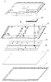
図1を参照して、ここで液晶表示装置におけるメインPWB150に対するガスケット90の取付構造について説明する。図1(a)に示すように、メインPWB150の接地(GND)が形成されているPWB裏面151に両面テープでガスケット(導電部材)190が固定される。そして、図1(b)に示すように、メインPWB150にガスケット190が固定された状態で、金属板部材130の背面側(図示上側)に樹脂製のバックキャビネット120が配置された状態のセットにおいて、バックキャビネット120に形成されたガスケット貫通用孔140を介して、ガスケット90が金属板部材130の所定の領域に両面テープにて貼り付けられる。その結果、図1(c)に示す構造となり、メインPWB150と金属板部材130とがガスケット190を介して適切に接触し、導通が確保されている。
With reference to FIG. 1, the attachment structure of the
この種の技術と様々なものが提案されている。例えば、アンテナを内蔵した通信携帯端末に対し、アンテナ特性の結果を防止しながら更なる薄型化を図った技術がある(特許文献1参照)。具体的には、第1板金をインサート成形した第1樹脂製キャビネットと、第2板金をインサート成型した第2樹脂製キャビネットとが設けられている。さらに、これら第1樹脂製キャビネットと第2樹脂製キャビネットとの間に、アンテナが印刷された回路基板が狭持されており、第1板金と第2板金とアンテナとが複数の導電性ガスケットによって電気的に接続されている。 This kind of technology and various things have been proposed. For example, there is a technique for further reducing the thickness of a communication portable terminal having a built-in antenna while preventing the result of antenna characteristics (see Patent Document 1). Specifically, a first resin cabinet in which the first sheet metal is insert-molded and a second resin cabinet in which the second sheet metal is insert-molded are provided. Further, a circuit board on which an antenna is printed is sandwiched between the first resin cabinet and the second resin cabinet, and the first sheet metal, the second sheet metal, and the antenna are separated by a plurality of conductive gaskets. Electrically connected.
ところで、ガスケット190の固定は両面テープのみでメインPWB150と金属板部材130に固定されている。しかも、バックキャビネット120のガスケット貫通用孔140を介しての固定であるため、このような構造を採用するテレビでは、両面テープの粘着性劣化や、組立時の貼り付け方のバラつき等の課題があった。例えば、図1(d)に示すように、ガスケット190が変形等によってガスケット貫通用孔140から外れることも想定される。それらの課題が顕在化した場合、メインPWB150と金属板部材130を導通させるガスケット190が接触の不安定となり不要輻射を悪化させたり、または、他の部品と接触し悪影響を及ぼすおそれがあった。また、そのような製品が市場に出荷されないようにするため、検査工程の手間が増えており、対策が必要とされていた。
By the way, the
また、特許文献1に開示の技術では、ガスケットを使用することで、離れた導電物を電気的に接続して有効活用している。また、両面テープによる固定や、中間の樹脂キャビネットに穴をあけて位置決めを行っている。しかし、ガスケットを圧縮することよる変形を抑制できず、接触不可領域に接触する可能性があるため別の技術が求められていた。また、両面テープなどの粘着物がはがれた場合、ガスケットが振動などで移動する可能性があり、対策が必要となることから別の技術が求められていた。 Moreover, in the technique disclosed in Patent Document 1, a conductive material is electrically connected and effectively used by using a gasket. In addition, positioning is performed by fixing with a double-sided tape or by making a hole in an intermediate resin cabinet. However, another technique has been demanded because deformation due to compression of the gasket cannot be suppressed and there is a possibility of contact with a non-contactable area. In addition, when an adhesive such as double-sided tape is peeled off, the gasket may move due to vibration or the like, and another countermeasure is required because countermeasures are required.
本発明は以上のような状況に鑑みなされたものであって、上記課題を解決する技術を提供することを目的とする。 This invention is made | formed in view of the above situations, Comprising: It aims at providing the technique which solves the said subject.
本発明の薄型表示装置は、バックライトユニットの背面側に対向して配置され、貫通孔を備えた非導電性板部材と、前記非導電性板部材に対して背面側に対向して配置された回路基板と、前記貫通孔に配置され、前記バックライトユニットの所定の接地領域と前記回路基板との導通を保持するガスケットと、を備え、前記非導電性板部材は、前記貫通孔の周囲が他の部分よりも厚く形成されたガスケット固定部を備える。
本発明の別の薄型表示装置は、バックライトユニットの背面側に対向して配置され、貫通孔を備えた非導電性のバックライトシャーシと、前記バックライトシャーシに対して背面側に対向して配置された回路基板と、前記貫通孔に配置され、前記バックライトユニットの所定の接地領域と前記回路基板との導通を保持するガスケットと、を備え、前記バックライトシャーシは、前記貫通孔の周囲が他の部分よりも厚く形成されたガスケット固定部を備える。
The thin display device of the present invention is arranged to face the back side of the backlight unit, and is arranged to face the back side with respect to the non-conductive plate member having a through hole and the non-conductive plate member. A circuit board, and a gasket disposed in the through hole and configured to maintain electrical connection between the predetermined ground region of the backlight unit and the circuit board, and the non-conductive plate member is disposed around the through hole. Includes a gasket fixing portion formed thicker than other portions.
Another thin display device of the present invention is disposed to face the back side of the backlight unit, and has a non-conductive backlight chassis provided with a through hole, and is opposed to the back side of the backlight chassis. A circuit board disposed, and a gasket disposed in the through hole and configured to maintain electrical connection between the predetermined ground region of the backlight unit and the circuit board, and the backlight chassis includes a periphery of the through hole. Includes a gasket fixing portion formed thicker than other portions.
本発明によれば、回路基板と金属部材を接触する際に貫通する樹脂製部材であるバックライトカバー(ミドルキャビ)の貫通穴の形状を、ガスケットを機械的に固定できるような構造に改善する技術を提供できる。 According to the present invention, the technology for improving the shape of the through hole of the backlight cover (middle cavity), which is a resin member that penetrates when the circuit board and the metal member are in contact, to a structure that can mechanically fix the gasket. Can provide.
次に、本発明を実施するための形態(以下、単に「実施形態」という)を、図面を参照して具体的に説明する。 Next, modes for carrying out the present invention (hereinafter, simply referred to as “embodiments”) will be specifically described with reference to the drawings.
<第1の実施形態>
図2は、本実施形態に係る液晶テレビ10の分解斜視図であり、正面側が図中下側に、背面側が図中上側になるように配置して模式的に表示している。
<First Embodiment>
FIG. 2 is an exploded perspective view of the
図示のように、表示パネル12の背面側(図中上側)にはバックライトユニット30が対向して配置されている。また、表示パネル12の前面側(図中下側)にはフロントキャビネット11が配置されている。
As shown in the figure, a
バックライトユニット30は、いわゆる直下型バックライトであって、金属板部材の前面側に複数のLEDが光源として配置されている。さらにバックライトユニット30の背面側には樹脂製のバックライトキャビネット20が対向して配置されている。そしてさらにその背面側の所定の領域にメインPWB50が対向して配置されている。さらに、メインPWB50が取り付けられたバックライトキャビネット20の背面側にはリヤキャビネット13が対向して配置される。
The
詳細は後述するが、バックライトキャビネット20にはバックライトキャビネット20の前後を連通するガスケット配置部40が設けられている。このガスケット配置部40に所定の大きさのガスケット90を配置し、バックライトユニット30の金属板部材の所定の長方形の領域35とメインPWB50の所定の接地回路領域(グランドパターン)とが電気的に接続している。
Although details will be described later, the
図3の斜視図は、バックライトキャビネット20及びメインPWB50に着目して示している。
The perspective view of FIG. 3 focuses on the
上述のように、バックライトキャビネット20の背面にはメインPWB50が配置・固定される。このとき、ガスケット90によって、メインPWB50はバックライトユニット30に対して接地される。メインPWB50の裏面側(図上側)の上面には、各種の処理用LSIや入出力端子等が配置されている。
As described above, the
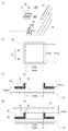
以下、図4及び図5を参照して接地の構造について説明する。ここで、図4は、接地構造のガスケット配置部に着目した図である。また、図5は、ガスケットによる接地構造の形成手順を示す図であり、特に図5(c)は図3のA−A断面に相当する。 Hereinafter, the grounding structure will be described with reference to FIGS. Here, FIG. 4 is a view focusing on the gasket arrangement portion of the ground structure. FIG. 5 is a diagram showing a procedure for forming a grounding structure using a gasket, and in particular, FIG. 5C corresponds to the AA cross section of FIG.
図示のように、バックライトキャビネット20には、ガスケット90を配置するためのガスケット配置部40が形成されている。なお、ガスケット90は、15mm×15mm×15mmのサイズの立方体であって、一定量押しつぶされることが可能なクッション性を有している。
As illustrated, the
ガスケット配置部40は、四角形のガスケット貫通用開口42と、そのガスケット貫通用開口42の四辺を囲む壁部44とから形成されている。なお、経年劣化によるガスケット90の落下等を考慮する観点からは、主に液晶テレビ10を立てて使用したときの下側に相当する領域を中心に壁部44が形成されていればよく、上辺に相当する領域に形成されなくともよい。ただし、メインPWB50等の移動に伴ってガスケット90がずれて変形する場合を考慮すると、上辺の領域にも形成されていることが好ましい。また、完全に壁面で形成するいつ様はなく、複数のピン状の構造が用いられてもよい。
The
ここでは、ガスケット貫通用開口42は、16mm×16mmのサイズである。したがって、ガスケット90が配置された状態で、ガスケット90とガスケット貫通用開口42の外周部分との間に上下左右0.5mmのギャップが形成されている。
Here, the
壁部44は、背面側に高さ3.5mmで凸状にガスケット貫通用開口42を囲む様に所定幅で形成されている。なお、バックライトキャビネット20の板状部分の厚さは3.0mmである。また、液晶テレビ10が適正に組み上がった状態で、バックライトユニット30(金属板部材32)とバックライトキャビネット20との距離は2.55mmである。さらに、壁部44の先端部とメインPWB50との距離は2.5mmである。つまり、バックライトユニット30の背面側の金属板部材32とメインPWB50との距離は11.55mmであり、ガスケット90は、3.45mm潰れた状態で固定される。なお、メインPWB50の前面側(図下側であり、バックライトキャビネット20に対向する面側)には、ガスケット90が固定される領域に接地領域として横18mm×縦15mmの長方形の領域35が確保されている。
The
ここで、ガスケットによる接地構造の配置手順を説明する。
まず、図5(a)に示すように、バックライトキャビネット20がバックライトユニット30の背面側に適正に配置された状態で、ガスケット配置部40にガスケット90が挿入され、バックライトユニット30の所定の接地用の領域35に配置される。このとき、ガスケット90は原形をとどめたままである。
Here, the arrangement | positioning procedure of the grounding structure by a gasket is demonstrated.
First, as shown in FIG. 5A, in a state where the
つづいて、図5(b)に示すように、ガスケット90の上から、つまり、背面側から、メインPWB50を配置する。このとき、メインPWB50とバックライトキャビネット20との距離は、図4(d)で説明したように、2.5mmに設定されている。したがって、図5(c)に示すようにメインPWB50がバックライトキャビネット20に固定されることで、ガスケット90は所定量だけ押しつぶされ固定される。ガスケット配置部40の壁部44の上端から突出するガスケット90の長さは、潰される前の8.95mmから5.5mmになる。
Subsequently, as shown in FIG. 5B, the
以上、本実施形態によると、ガスケット固定の機械的強度が確保される。つまり、ガスケット90の側面に対向する幅及び面積が増加する。このため、ガスケット90の取り付け作業時に、ガスケット90の形状変形をコントロールすることができる。したがって、振動等によるズレを抑制や、ガスケット90の取り付け作業時の位置決めが容易になる。また、メインPWB50と、LEDを配置している金属板部材(バックライトユニット30)の安定的な接触・導通を確保し、不要輻射悪化を抑制できる。
As mentioned above, according to this embodiment, the mechanical strength of gasket fixation is ensured. That is, the width and area facing the side surface of the
<第2の実施形態>
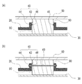
図6は第2の実施形態に係るガスケット配置部40を示した図である。例えば図6(a)に示すように、壁部44の内面に爪状の係止構造46が形成されてもよい。ガスケット90の固定が一層強固になる。係止構造46は、内面全周にわたって形成されてもよいし、一部領域のみに形成されてもよい。また、係止構造46の大きさは、ガスケット90を配置するときの作業性、潰れたときの変形量及び固定力のバランスを考慮して設定されており、例えば、上記ガスケット90とガスケット配置部40とのギャップに相当する0,5mm程度である。また、図6(b)に示すように、壁部44の対向する2カ所に穴48が設けられ、固定用バー49がガスケット90を突き刺し貫通するように、それら穴48に取り付けられてもよい。なお、ガスケット90を貫通する固定用バー49は一本でなく、複数であってもよく、貫通しない構成が用いられてもよい。
<Second Embodiment>
FIG. 6 is a view showing a
また、特に図示はしないが、ガスケット配置部40の壁部44の高さをガスケット90のクッション部分の面のみ低くしてもよい。潰されたガスケット90のクッションの逃げ場をつくり、ガスケット90が変形した場合に、グランドパターン以外への接触を防止することができる。
Although not particularly shown, the height of the
<第3の実施形態>
図7は第3の実施形態に係るガスケット配置部240、340を示す図であって、図4(b)に対応する図である。
<Third Embodiment>
FIG. 7 is a view showing
図7(a)に示すガスケット配置部240は、ガスケット貫通用開口42の周囲を囲む上述の壁部44に対応する構成として、ガスケット貫通用開口42の四隅に形成された第1〜第4の突起部244a〜244dを備える。第1〜第4の突起部244a〜244dは、上面視でL字状のリブ突起構造となっている。
The
図7(b)に示すガスケット配置部340は、ガスケット貫通用開口42の周囲を囲む上述の壁部44に対応する構成として、ガスケット貫通用開口42の四辺近傍に板状(リブ状)の第1〜第4の壁部344a〜344dを備える。図7(a)の構成とは反対に、上述の壁部44の四隅を取り除いた構成となっている。
The
これらの構造とすることで、ガスケット90が潰されて変形した場合、潰れた部分が第1〜第4の突起部244a〜244dや第1〜第4の壁部344a〜344dが形成されていない4箇所の空間に嵌まることから、あらゆる方向の振動に対してガスケット90の位置維持機能が良好に作用する。
With these structures, when the
<第4の実施形態>
図8は第4の実施形態に係るガスケット配置部440を示す断面側面図であって、図5に対応している。ガスケット配置部440は、ガスケット貫通用開口442を囲むように、上下に突出する、つまり、メインPWB50及びバックライトユニット30の両方の側に突出する壁部444が形成されている。そして、壁部444の内壁面はバックライトユニット30側が広がるようにガスケット貫通用開口442が形成されている。つまり、ガスケット貫通用開口442は截頭四角錐になっている。ガスケット貫通用開口442の上側の大きさは、ガスケット90の外形と略同一になっている。
<Fourth Embodiment>
FIG. 8 is a cross-sectional side view showing a
図8(a)の様に、上からガスケット90がガスケット貫通用開口442に挿入され、図8(b)の状態になる。図8(b)の状態では壁部444とガスケット90の間には所定の空間Xが形成されている。そして、図8(c)の様に、メインPWB50が取り付けられガスケット90が潰れて変形するときに、壁部444とガスケット90の間の空間Xに、変形部分が膨らむようになっている。その結果、メインPWB50側には変形部分がはみ出ないようになっている。したがって、ガスケット90がメインPWB50に搭載される部品や配線に対して悪影響を与えることがない。
As shown in FIG. 8A, the
<第5の実施形態>
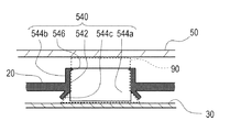
図9は第5の実施形態に係るガスケット配置部540を示す断面側面図である。このガスケット配置部540では、ガスケット貫通用開口542の上側を囲むように形成された上側壁部544aと、下側に形成された第1の下側壁部544b及び第2の下側壁部544cとを有する。上側壁部544aは、図6(a)で示した壁部40と同様の構造となっており、上側壁部544aの内面上側に爪状の係止構造546が形成されている。係止構造546に係止されるガスケット90には係止位置を決めるための所定の切り目や凹状形状が形成されている。
<Fifth Embodiment>
FIG. 9 is a cross-sectional side view showing a
第1の下側壁部544bは、図示で奥側及び手前側(図示せず)の2つの壁部が対応している。これら第1の下側壁部544bは、鉛直に所定長だけ下方向に延びるリブ状に形成されている。第2の下側壁部544cは、図示で左右の2つの壁部が対応している。これら第2の下側壁部544cは、外方向に広がる構造となっておいる。
The first
このような構造によって、ガスケット配置部540に取り付けられたガスケット90は、押しつぶされて変形する場合に、変形部分は外方向に広がる第2の下側壁部544cに誘導される。
With such a structure, when the
以上、本発明を実施形態をもとに説明した。この実施形態は例示であり、それらの各構成要素の組み合わせ等にいろいろな変形例が可能なこと、またそうした変形例も本発明の範囲にあることは当業者に理解されるところである。 The present invention has been described based on the embodiments. This embodiment is an exemplification, and it is understood by those skilled in the art that various modifications can be made to combinations of the respective components and the like, and such modifications are within the scope of the present invention.
10 液晶テレビ
11 フロントキャビネット
12 表示パネル
13 リヤキャビネット
20 バックライトキャビネット
30 バックライトユニット
32 金属板部材
35 領域
40、240、340、440、540 ガスケット配置部
42、442、542 ガスケット貫通用開口
44、444 壁部
46、546 係止構造
48 穴
49 固定用バー
50 メインPWB
90 ガスケット
244a〜244d 第1〜第4の突起部
344a〜344d 第1〜第4の壁部
544a 上側壁部
544b 第1の下側壁部
544c 第2の下側壁部
DESCRIPTION OF
90
Claims (2)
前記非導電性板部材に対して背面側に対向して配置された回路基板と、
前記貫通孔に配置され、前記バックライトユニットの所定の接地領域と前記回路基板との導通を保持するガスケットと、
を備え、
前記非導電性板部材は、前記貫通孔の周囲が他の部分よりも厚く形成されたガスケット固定部を備えることを特徴とする薄型表示装置。 A non-conductive plate member disposed opposite the back side of the backlight unit and provided with a through hole;
A circuit board disposed on the back side of the non-conductive plate member;
A gasket that is disposed in the through-hole and maintains electrical connection between a predetermined ground region of the backlight unit and the circuit board;
With
The non-conductive plate member includes a gasket fixing portion in which a periphery of the through hole is formed thicker than other portions.
前記バックライトシャーシに対して背面側に対向して配置された回路基板と、
前記貫通孔に配置され、前記バックライトユニットの所定の接地領域と前記回路基板との導通を保持するガスケットと、
を備え、
前記バックライトシャーシは、前記貫通孔の周囲が他の部分よりも厚く形成されたガスケット固定部を備えることを特徴とする薄型表示装置。 A non-conductive backlight chassis provided with a through-hole, facing the back side of the backlight unit,
A circuit board disposed opposite to the back side of the backlight chassis;
A gasket that is disposed in the through-hole and maintains electrical connection between a predetermined ground region of the backlight unit and the circuit board;
With
The thin-type display device, wherein the backlight chassis includes a gasket fixing portion in which a periphery of the through hole is formed thicker than other portions.
Priority Applications (1)
| Application Number | Priority Date | Filing Date | Title |
|---|---|---|---|
| JP2015084639A JP2015166876A (en) | 2013-02-14 | 2015-04-17 | Thin display device |
Applications Claiming Priority (3)
| Application Number | Priority Date | Filing Date | Title |
|---|---|---|---|
| JP2013026554 | 2013-02-14 | ||
| JP2013026554 | 2013-02-14 | ||
| JP2015084639A JP2015166876A (en) | 2013-02-14 | 2015-04-17 | Thin display device |
Related Parent Applications (1)
| Application Number | Title | Priority Date | Filing Date |
|---|---|---|---|
| JP2014121385A Division JP5736492B2 (en) | 2013-02-14 | 2014-06-12 | Thin display device |
Publications (1)
| Publication Number | Publication Date |
|---|---|
| JP2015166876A true JP2015166876A (en) | 2015-09-24 |
Family
ID=51698637
Family Applications (2)
| Application Number | Title | Priority Date | Filing Date |
|---|---|---|---|
| JP2014121385A Expired - Fee Related JP5736492B2 (en) | 2013-02-14 | 2014-06-12 | Thin display device |
| JP2015084639A Pending JP2015166876A (en) | 2013-02-14 | 2015-04-17 | Thin display device |
Family Applications Before (1)
| Application Number | Title | Priority Date | Filing Date |
|---|---|---|---|
| JP2014121385A Expired - Fee Related JP5736492B2 (en) | 2013-02-14 | 2014-06-12 | Thin display device |
Country Status (1)
| Country | Link |
|---|---|
| JP (2) | JP5736492B2 (en) |
Families Citing this family (2)
| Publication number | Priority date | Publication date | Assignee | Title |
|---|---|---|---|---|
| KR102185519B1 (en) | 2019-02-13 | 2020-12-02 | 주식회사 싸이큐어 | Method of garbling real-world image for direct encoding type see-through head mount display and direct encoding type see-through head mount display with real-world image garbling function |
| KR20200099047A (en) | 2019-02-13 | 2020-08-21 | 주식회사 싸이큐어 | Method of garbling real-world image for see-through head mount display and see-through head mount display with real-world image garbling function |
Citations (10)
| Publication number | Priority date | Publication date | Assignee | Title |
|---|---|---|---|---|
| JPS62238692A (en) * | 1986-04-10 | 1987-10-19 | キヤノン株式会社 | Electronic equipment |
| JPH09218649A (en) * | 1996-02-09 | 1997-08-19 | Matsushita Electric Ind Co Ltd | Liquid crystal display device and its shielding plate |
| JP2003015150A (en) * | 2001-06-28 | 2003-01-15 | Aiphone Co Ltd | Conductive connecting structure for liquid crystal panel |
| JP2005209868A (en) * | 2004-01-22 | 2005-08-04 | Casio Comput Co Ltd | Electronic apparatus |
| JP2010165440A (en) * | 2009-01-19 | 2010-07-29 | Sharp Corp | Disk drive mount type display device, and display unit |
| JP2012047838A (en) * | 2010-08-25 | 2012-03-08 | Funai Electric Co Ltd | Fixing structure of x-printed circuit board of liquid crystal module |
| US20120182515A1 (en) * | 2011-01-19 | 2012-07-19 | Pyo Si-Baek | Liquid crystal display apparatus |
| WO2012117657A1 (en) * | 2011-02-28 | 2012-09-07 | パナソニック株式会社 | Display device |
| WO2012165324A1 (en) * | 2011-06-02 | 2012-12-06 | シャープ株式会社 | Lighting device, display device, and television receiver |
| JP2014178677A (en) * | 2013-02-14 | 2014-09-25 | Sharp Corp | Thin display device |
-
2014
- 2014-06-12 JP JP2014121385A patent/JP5736492B2/en not_active Expired - Fee Related
-
2015
- 2015-04-17 JP JP2015084639A patent/JP2015166876A/en active Pending
Patent Citations (10)
| Publication number | Priority date | Publication date | Assignee | Title |
|---|---|---|---|---|
| JPS62238692A (en) * | 1986-04-10 | 1987-10-19 | キヤノン株式会社 | Electronic equipment |
| JPH09218649A (en) * | 1996-02-09 | 1997-08-19 | Matsushita Electric Ind Co Ltd | Liquid crystal display device and its shielding plate |
| JP2003015150A (en) * | 2001-06-28 | 2003-01-15 | Aiphone Co Ltd | Conductive connecting structure for liquid crystal panel |
| JP2005209868A (en) * | 2004-01-22 | 2005-08-04 | Casio Comput Co Ltd | Electronic apparatus |
| JP2010165440A (en) * | 2009-01-19 | 2010-07-29 | Sharp Corp | Disk drive mount type display device, and display unit |
| JP2012047838A (en) * | 2010-08-25 | 2012-03-08 | Funai Electric Co Ltd | Fixing structure of x-printed circuit board of liquid crystal module |
| US20120182515A1 (en) * | 2011-01-19 | 2012-07-19 | Pyo Si-Baek | Liquid crystal display apparatus |
| WO2012117657A1 (en) * | 2011-02-28 | 2012-09-07 | パナソニック株式会社 | Display device |
| WO2012165324A1 (en) * | 2011-06-02 | 2012-12-06 | シャープ株式会社 | Lighting device, display device, and television receiver |
| JP2014178677A (en) * | 2013-02-14 | 2014-09-25 | Sharp Corp | Thin display device |
Also Published As
| Publication number | Publication date |
|---|---|
| JP2014178710A (en) | 2014-09-25 |
| JP5736492B2 (en) | 2015-06-17 |
Similar Documents
| Publication | Publication Date | Title |
|---|---|---|
| US7221414B2 (en) | Liquid crystal display device with perforated joint pieces attachable by screws | |
| US20150055053A1 (en) | Display device and support member thereof | |
| US9274359B2 (en) | Electronic device display chassis | |
| US11093006B2 (en) | Display module and display device | |
| JP4212062B1 (en) | LCD panel | |
| US20150313030A1 (en) | Pedestal for flat panel display device and flat panel display device | |
| US8118472B2 (en) | Fixing structure for printed circuit board of backlight module | |
| JP5736492B2 (en) | Thin display device | |
| EP2584398A2 (en) | Display | |
| CN103544884A (en) | Display device with external force transmission structure | |
| US8970793B2 (en) | Display device, and television device | |
| JP2009053399A (en) | Image display device | |
| JP5563728B1 (en) | Thin display device | |
| US9535286B2 (en) | Image display device | |
| JP2005123257A (en) | Connection structure of printed circuit board integrally formed with connector | |
| JP5865887B2 (en) | Display device | |
| US20090161304A1 (en) | Frame for flat panel display | |
| JP6111553B2 (en) | Display device and television device | |
| US20140321078A1 (en) | Display device | |
| JP2013092655A (en) | Display device and television device | |
| JP2011053447A (en) | Plasma display device | |
| US10018862B2 (en) | Frame component and display device | |
| CN220709897U (en) | Display device | |
| KR20170072399A (en) | Guide pin and video wall using the same | |
| KR100508771B1 (en) | Display device |
Legal Events
| Date | Code | Title | Description |
|---|---|---|---|
| A131 | Notification of reasons for refusal |
Free format text: JAPANESE INTERMEDIATE CODE: A131 Effective date: 20160105 |
|
| A02 | Decision of refusal |
Free format text: JAPANESE INTERMEDIATE CODE: A02 Effective date: 20160510 |