JP2015154352A - sensitivity adjustment circuit - Google Patents
sensitivity adjustment circuit Download PDFInfo
- Publication number
- JP2015154352A JP2015154352A JP2014027800A JP2014027800A JP2015154352A JP 2015154352 A JP2015154352 A JP 2015154352A JP 2014027800 A JP2014027800 A JP 2014027800A JP 2014027800 A JP2014027800 A JP 2014027800A JP 2015154352 A JP2015154352 A JP 2015154352A
- Authority
- JP
- Japan
- Prior art keywords
- adjustment
- voltage
- sample
- amplifier
- input
- Prior art date
- Legal status (The legal status is an assumption and is not a legal conclusion. Google has not performed a legal analysis and makes no representation as to the accuracy of the status listed.)
- Pending
Links
Images


Abstract
Description
本発明は、感度調整回路に関し、より詳細には、感度調整量に対して素子ばらつきがあっても広範囲に線形性を確保するようにした感度調整回路に関する。特に、圧力センサ、温度センサ、加速度センサ、角速度センサ、磁気センサなどの感度調整回路に適用できる。 The present invention relates to a sensitivity adjustment circuit, and more particularly to a sensitivity adjustment circuit that ensures linearity over a wide range even if there is element variation with respect to the sensitivity adjustment amount. In particular, the present invention can be applied to sensitivity adjustment circuits such as pressure sensors, temperature sensors, acceleration sensors, angular velocity sensors, and magnetic sensors.
従来から、各種センサデバイス等からの入力信号に対する出力信号の感度を調整する方法として、様々な技術がある。
特許文献1には、電源電圧変動および温度変動に対してセンサの感度を調整する回路に関するもので、温度センサ117と、供給電圧106と、温度センサ117及び供給電圧106からの信号を信号処理するマイコン3と、マイコン3からのアナログ信号によりゲイン調整回路115と、温度補正116とを備える回路が開示されている。
また、特許文献2には、センサからの信号を入力し、可変抵抗回路および演算増幅器を有する可変利得増幅回路と、この可変利得増幅回路に温度変動感度調整電圧を与える第1電圧供給手段と、可変利得増幅回路に電源電圧変動感度調整電圧を与える第2電圧供給手段とを備えた感度調整回路が開示されている。可変利得増幅回路は、温度変動感度調整電圧及び電源電圧変動感度調整電圧に基づいて、電源電圧変動及び温度変動に対してセンサの感度を調整する。
Conventionally, there are various techniques for adjusting the sensitivity of an output signal with respect to an input signal from various sensor devices.
Patent Document 1 relates to a circuit that adjusts the sensitivity of a sensor with respect to power supply voltage fluctuation and temperature fluctuation, and performs signal processing on a temperature sensor 117, a supply voltage 106, and signals from the temperature sensor 117 and the supply voltage 106. A circuit including a
Further,
しかしながら、従来の感度調整回路では、以下のような課題があった。
上述した特許文献1では、ADCとDACを用いているため、感度調整量が離散的になる。一般的にセンサは、広い調整範囲と感度調整量に関して線形性を必要とする。そのため、離散的な場合、線形性が不十分である。または、十分な調整範囲で調整するためには、ADCとDACのbit数を増やす必要があり回路が大規模になってしまう。
また、上述した特許文献2の感度調整回路では、連続的な調整になってはいるが、閾値電圧VR等の素子のミスマッチにより、感度調整に対して非線形性が生じてしまうという問題がある。
However, the conventional sensitivity adjustment circuit has the following problems.
In Patent Document 1 described above, since the ADC and the DAC are used, the sensitivity adjustment amount is discrete. In general, a sensor requires linearity with respect to a wide adjustment range and sensitivity adjustment amount. Therefore, in the discrete case, the linearity is insufficient. Or, in order to adjust within a sufficient adjustment range, it is necessary to increase the number of bits of ADC and DAC, resulting in a large-scale circuit.
Further, although the sensitivity adjustment circuit of
本発明は、このような問題を鑑みてなされたもので、その目的とするところは、感度調整量に対して素子ばらつきがあっても広範囲に線形性を確保する感度調整回路を提供することにある。 The present invention has been made in view of such problems, and an object of the present invention is to provide a sensitivity adjustment circuit that ensures linearity over a wide range even if there is element variation with respect to the sensitivity adjustment amount. is there.
本発明は、このような目的を達成するためになされたもので、請求項1に記載の発明は、利得調整電圧(VG)に基づいて利得が調整される可変利得増幅器(11,31)と、前記可変利得増幅器(11,31)に入力する信号を、入力電圧(Vin)と第1調整電圧(VA1)とで切り替える入力切替部(13,33)と、前記可変利得増幅器(11,31)の出力電圧(Vout)と第2調整電圧(VA2)が入力される増幅器(12,32)と、前記増幅器(12,32)の出力をサンプル/ホールドして利得調整電圧(VG)を生成するサンプル/ホールド部(14,34)とを備え、利得調整区間では、前記入力切替部(13,33)を切り替えて前記可変利得増幅器(11,31)に前記第1調整電圧(VA1)が入力されて、前記サンプル/ホールド部(14,34)が前記増幅器(12,32)の出力をサンプル/ホールドし、測定区間では、前記入力切替部(13,33)を切り替えて前記可変利得増幅器(11,31)に前記入力電圧(Vin)が入力されて、前記サンプル/ホールド部(14,34)がホールドした前記利得調整電圧(VG)に基づいて入力電圧(Vin)が調整されて出力されることを特徴とする感度調整回路である。(全実施例;図2,図6,図9) The present invention has been made to achieve such an object, and the invention according to claim 1 includes a variable gain amplifier (11, 31) whose gain is adjusted based on a gain adjustment voltage (VG). , An input switching unit (13, 33) for switching a signal input to the variable gain amplifier (11, 31) between an input voltage (Vin) and a first adjustment voltage (VA1), and the variable gain amplifier (11, 31). ) To which the output voltage (Vout) and the second adjustment voltage (VA2) are input, and the output of the amplifier (12, 32) is sampled / held to generate the gain adjustment voltage (VG) And a sample / hold unit (14, 34) for switching, the input switching unit (13, 33) is switched in the gain adjustment section, and the first adjustment voltage (VA1) is supplied to the variable gain amplifier (11, 31). Entered, The sample / hold unit (14, 34) samples / holds the output of the amplifier (12, 32). In the measurement period, the input switching unit (13, 33) is switched to switch the variable gain amplifier (11, 31). ) Is input to the input voltage (Vin), and the input voltage (Vin) is adjusted and output based on the gain adjustment voltage (VG) held by the sample / hold unit (14, 34). This is a characteristic sensitivity adjustment circuit. (All examples; FIG. 2, FIG. 6, FIG. 9)
また、請求項2に記載の発明は、請求項1に記載の発明において、前記サンプル/ホールド部(14,34)は、サンプル/ホールドを切り替える第1サンプル/ホールドスイッチ(14a)と、第1容量素子(C1)とを備えていることを特徴とする。(実施例1,2;図2,図6)
また、請求項3に記載の発明は、請求項1又は2に記載の発明において、前記測定区間において、前記可変利得増幅器(11,31)の利得が、第2調整電圧(VA2)/第1調整電圧(VA1)に比例する利得であることを特徴とする。
According to a second aspect of the present invention, in the first aspect of the present invention, the sample / hold unit (14, 34) includes a first sample / hold switch (14a) for switching the sample / hold, And a capacitor element (C1). (Examples 1 and 2; FIGS. 2 and 6)
According to a third aspect of the present invention, in the first or second aspect of the present invention, in the measurement section, the gain of the variable gain amplifier (11, 31) is a second adjusted voltage (VA2) / first. The gain is proportional to the adjustment voltage (VA1).
また、請求項4に記載の発明は、請求項1乃至3のいずれかに記載の発明において、前記測定区間において、前記入力電圧(Vin)が、第2調整電圧(VA2)/第1調整電圧(VA1)に比例する利得で調整されて出力されることを特徴とする。
また、請求項5に記載の発明は、請求項2に記載の発明において、前記サンプル/ホールド部(14,34)は、前記第1容量素子(C1)とローパスフィルタ(LPF)を形成する第1抵抗素子(R1)をさらに備えていることを特徴とする。
According to a fourth aspect of the present invention, in the invention according to any one of the first to third aspects, the input voltage (Vin) is a second adjustment voltage (VA2) / first adjustment voltage in the measurement section. The output is adjusted with a gain proportional to (VA1).
According to a fifth aspect of the present invention, in the second aspect of the present invention, the sample / hold unit (14, 34) includes a first low-pass filter (LPF) and the first capacitive element (C1). It further includes a one-resistance element (R1).
また、請求項6に記載の発明は、請求項1乃至5のいずれかに記載の発明において、第1調整電圧生成回路(21)と、第2調整電圧生成回路(22)とをさらに備え、前記第1調整電圧生成回路(21)は、第1調整電圧(VA1)を生成し、前記第2調整電圧生成回路(22)は、第2調整電圧(VA2)を生成することを特徴とする。(実施例1;図1)
また、請求項7に記載の発明は、請求項6に記載の発明において、前記第1調整電圧生成回路(21)が、温度センサ(41)であり、前記第2調整電圧生成回路(22)が、電源電圧依存電圧供給回路(42)であることを特徴とする。(実施例2;図5)
The invention according to claim 6 is the invention according to any one of claims 1 to 5, further comprising a first adjustment voltage generation circuit (21) and a second adjustment voltage generation circuit (22), The first adjustment voltage generation circuit (21) generates a first adjustment voltage (VA1), and the second adjustment voltage generation circuit (22) generates a second adjustment voltage (VA2). . (Example 1; FIG. 1)
According to a seventh aspect of the invention, in the sixth aspect of the invention, the first adjustment voltage generation circuit (21) is a temperature sensor (41), and the second adjustment voltage generation circuit (22). Is a power supply voltage dependent voltage supply circuit (42). (Example 2; FIG. 5)
また、請求項8に記載の発明は、利得調整電圧(VG)に基づいて利得が調整される可変利得増幅器(51)と、前記可変利得増幅器(51)に入力する信号を、入力電圧(Vin)と第1調整電圧(VA1)とで切り替える入力切替部(53)と、前記可変利得増幅器(51)の出力電圧(Vout)と第2調整電圧(VA2)が入力される増幅器(52)と、前記増幅器(52)の入力極性を切り替える極性切替部(55)と、前記増幅器(52)の出力をサンプル/ホールドして利得調整電圧を生成するサンプル/ホールド部(54)とを備え、第1利得調整区間では、前記可変利得増幅器(51)に前記第1調整電圧(VA1)が入力され、前記増幅器(52)に第2調整電圧(VA2)が入力され、前記サンプル/ホールド部(54)が前記増幅器(52)の第1出力をサンプル/ホールドし、第2利得調整区間では、前記可変利得増幅器(51)に極性が反転した前記第1調整電圧(VA1)が入力され、前記増幅器(52)に極性が反転した第2調整電圧(VA2)が入力され、前記増幅器(52)の入力極性が切り替えられ、前記サンプル/ホールド部(54)が前記増幅器(52)の第2出力をサンプル/ホールドし、測定区間では、前記可変利得増幅器(51)に前記入力電圧(Vin)が入力されて、前記サンプル/ホールド部(54)がホールドした前記第1出力及び第2出力を平均化した利得調整電圧(VG)に基づいて入力電圧が調整されて出力されることを特徴とする感度調整回路である。(実施例3;図9)
また、請求項9に記載の発明は、請求項8に記載の発明において、前記サンプル/ホールド部(54)は、第1調整区間でサンプル/ホールドを切り替える、第1サンプル/ホールドスイッチ(54−1)と第2サンプル/ホールドスイッチ(54−2)及び第1容量素子(C1)と、第2調整区間でサンプル/ホールドを切り替える、第3サンプル/ホールドスイッチ(54−3)と第4サンプル/ホールドスイッチ(54−4)及び第2容量素子(C2)とを備えていることを特徴とする。
According to an eighth aspect of the present invention, a variable gain amplifier (51) whose gain is adjusted based on a gain adjustment voltage (VG) and a signal input to the variable gain amplifier (51) are input voltage (Vin). ) And the first adjustment voltage (VA1), an input switching unit (53), an output voltage (Vout) of the variable gain amplifier (51), and an amplifier (52) to which the second adjustment voltage (VA2) is input. A polarity switching unit (55) for switching the input polarity of the amplifier (52), and a sample / hold unit (54) for sampling / holding the output of the amplifier (52) to generate a gain adjustment voltage. In the one gain adjustment section, the first adjustment voltage (VA1) is input to the variable gain amplifier (51), the second adjustment voltage (VA2) is input to the amplifier (52), and the sample / hold unit (5 ) Samples / holds the first output of the amplifier (52), and in the second gain adjustment section, the variable voltage amplifier (51) receives the first adjustment voltage (VA1) whose polarity is inverted, and the amplifier The second adjustment voltage (VA2) whose polarity is inverted is input to (52), the input polarity of the amplifier (52) is switched, and the sample / hold unit (54) outputs the second output of the amplifier (52). In the measurement period, the input voltage (Vin) is input to the variable gain amplifier (51), and the first output and the second output held by the sample / hold unit (54) are averaged in the measurement period. The sensitivity adjustment circuit is characterized in that the input voltage is adjusted and output based on the gain adjustment voltage (VG). (Example 3; FIG. 9)
The invention according to claim 9 is the first sample / hold switch (54-) according to the invention according to claim 8, wherein the sample / hold unit (54) switches the sample / hold in the first adjustment section. 1), the second sample / hold switch (54-2) and the first capacitor element (C1), and the third sample / hold switch (54-3) and the fourth sample for switching the sample / hold in the second adjustment section. / Hold switch (54-4) and a second capacitor element (C2).
また、請求項10に記載の発明は、請求項8又は9に記載の発明において、前記第1調整区間では、第1サンプル/ホールドスイッチ(54−1)と第2サンプル/ホールドスイッチ(54−2)とで、第1容量素子(C1)に前記増幅器(52)の第1出力をサンプル/ホールドし、前記第2調整区間では、第3サンプル/ホールドスイッチ(54−3)と第4サンプル/ホールドスイッチ(54−4)とで、第2容量素子(C2)に前記増幅器(52)の第2出力をサンプル/ホールドし、前記測定区間では、第2サンプル/ホールドスイッチ(54−2)と第4サンプル/ホールドスイッチ(54−4)で、前記第1容量素子(C1)及び前記第2容量素子(C2)がホールドした前記第1出力及び第2出力を平均化して利得調整電圧(VG)を生成することを特徴とする。
Further, in the invention described in
また、請求項11に記載の発明は、請求項8,9又は10に記載の発明において、第1調整電圧生成回路と、第2調整電圧生成回路とをさらに備え、前記第1調整電圧生成回路は、第1調整区間では、第1調整電圧(VA1)を生成し、第2調整区間では、極性が反転した第1調整電圧(VA1)を生成し、前記第2調整電圧生成回路は、第1調整区間では、第2調整電圧(VA2)を生成し、第2調整区間では、極性が反転した第2調整電圧(VA2)を生成することを特徴とする。
また、請求項12に記載の発明は、請求項1乃至11のいずれかに記載の発明において、前記第1調整電圧(VA1)は、温度依存電圧であり、前記第2調整電圧(VA2)は、電源電圧依存電圧であることを特徴とする。
The invention according to
The invention according to
本発明によれば、感度調整量に対して素子ばらつきがあっても広範囲に線形性を確保する感度調整回路を実現することができる。
また、感度調整回路に第1調整電圧を供給する第1調整電圧生成回路と、感度調整回路に第2調整電圧を供給する第2調整電圧生成回路とを備え、第1調整電圧と第2調整電圧を基に、入力信号に対する出力信号の感度を調整することができる。
また、第1調整電圧及び第2調整電圧を、それぞれ温度補正するための温度依存調整電圧、電源電圧依存性を持たせるための電源電圧依存調整電圧とすることで、入力信号に対して、電源電圧依存性と温度補正を行うことができる。
According to the present invention, it is possible to realize a sensitivity adjustment circuit that ensures linearity over a wide range even if there is an element variation with respect to the sensitivity adjustment amount.
A first adjustment voltage generation circuit for supplying a first adjustment voltage to the sensitivity adjustment circuit; and a second adjustment voltage generation circuit for supplying a second adjustment voltage to the sensitivity adjustment circuit. Based on the voltage, the sensitivity of the output signal relative to the input signal can be adjusted.
Further, the first adjustment voltage and the second adjustment voltage are respectively a temperature-dependent adjustment voltage for temperature correction and a power-supply voltage-dependent adjustment voltage for providing power supply voltage dependency, so that a power supply can be supplied to an input signal. Voltage dependence and temperature correction can be performed.
以下、図面を参照して本発明の各実施形態について説明する。
<実施形態1>
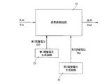
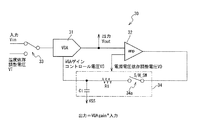
図1は、本発明に係る感度調整回路の実施形態1を説明するためのブロック図である。図中符号10は感度調整回路、21は第1調整電圧生成回路、22は第2調整電圧生成回路を示している。
本実施形態1の感度調整回路は、異なる2つの調整電圧に対して感度を調整する感度調整回路であって、入力電圧Vinを入力し、出力電圧Voutを出力する感度調整回路10と、この感度調整回路10に第1調整電圧VA1を供給する第1調整電圧生成回路21と、感度調整回路10に第2調整電圧VA2を供給する第2調整電圧生成回路22とを備えている。
Hereinafter, each embodiment of the present invention will be described with reference to the drawings.
<Embodiment 1>
FIG. 1 is a block diagram for explaining a first embodiment of a sensitivity adjustment circuit according to the present invention. In the figure,
The sensitivity adjustment circuit according to the first embodiment is a sensitivity adjustment circuit that adjusts sensitivity with respect to two different adjustment voltages. The
つまり、感度調整回路10は、入力信号Vinに対して感度を調整して出力する。第1調整電圧生成回路21は、第1調整電圧VA1を感度調整回路10に供給する。また、第2調整電圧生成回路22は、第2調整電圧VA2を感度調整回路10に供給する。
感度調整回路10は、第1調整電圧VA1と第2調整電圧VA2を基に、入力信号Vinに対する出力信号Voutの感度を調整することができる。
That is, the
The
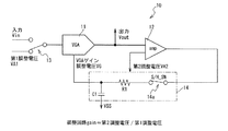
図2は、図1に示した実施形態1に基づいた実施例1を説明するための感度調整回路の回路構成図である。図中符号11は可変利得増幅器(VGA;variable gain amplifier)、12は増幅器(amp)、13は入力切替部(SW)、14はサンプル/ホールド部、14aはサンプル/ホールドスイッチ(S/H_SW)を示している。
可変利得増幅器(VGA)11は、利得調整電圧VGに基づいて利得が調整される。入力切替部(SW)13は、可変利得増幅器11に入力する信号を、入力電圧Vinと第1調整電圧VA1とで切り替える。
FIG. 2 is a circuit configuration diagram of a sensitivity adjustment circuit for explaining Example 1 based on Embodiment 1 shown in FIG. In the figure,
The gain of the variable gain amplifier (VGA) 11 is adjusted based on the gain adjustment voltage VG. The input switching unit (SW) 13 switches a signal input to the
増幅器12は、可変利得増幅器11の出力電圧Voutと第2調整電圧VA2が入力される。サンプル/ホールド部14は、サンプル/ホールドを切り替える第1サンプル/ホールドスイッチ14aと第1容量素子C1とを備え、増幅器12の出力をサンプル/ホールドして利得調整電圧を生成する。
このような構成により、利得調整区間では、入力切替部13を切り替えて可変利得増幅器11に第1調整電圧VA1が入力されて、サンプル/ホールド部14が増幅器12の出力をサンプル/ホールドする。
The
With such a configuration, in the gain adjustment section, the
測定区間では、入力切替部13を切り替えて可変利得増幅器11に入力電圧Vinが入力されて、サンプル/ホールド部14がホールドした利得調整電圧VGに基づいて入力電圧Vinが調整されて出力される。
また、測定区間において、可変利得増幅器11の利得が、第2調整電圧VA2/第1調整電圧VA1に比例する利得である。また、測定区間において、入力電圧Vinが、第2調整電圧VA2/第1調整電圧VA1に比例する利得で調整されて出力される。
また、サンプル/ホールド部14は、第1容量素子C1とローパスフィルタLPFを形成する第1抵抗素子R1をさらに備えている。
In the measurement interval, the
In the measurement section, the gain of the
The sample /
このように、本実施例1の感度調整回路は、可変利得増幅回路(VGA)11と増幅器12と、切り替えスイッチ13とS/Hスイッチ(サンプル/ホールドスイッチ)14aとを備えている。また、電圧を保持するための容量素子C1と、増幅器12のノイズを低減するための、容量素子C1とフィルタを形成する抵抗素子R1とを備えている。
VGA11は、VGAゲイン調整電圧に応じて、VGA11の入出力のゲインを決定する。入力切り替えスイッチ13は、入力信号Vinと第1調整電圧VA1とを切り替えてVGA11の入力に電圧を供給する。
As described above, the sensitivity adjustment circuit according to the first embodiment includes the variable gain amplifier circuit (VGA) 11, the
The
増幅器12は、VGA11の出力と第2調整電圧VA2の差を増幅して出力する。S/H_SW14aは、感度調整回路10のループの形成と切断を切り替える。
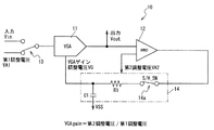
図3は、図2に示した実施例1におけるゲイン調整時の感度調整回路を示す回路構成図である。以下に、感度調整回路10のゲイン調整時の動作について説明する。
入力切り替えスイッチ13は、第1調整電圧VA1を選択してVGA11の入力とする。S/H_SW14aがONとなり、増幅器12の出力がVGAゲイン調整電圧VGとなる。この時、感度調整回路10で形成されるフィードバックループにより、VGA11の出力が、第2調整電圧VA2となるようにVGAゲイン調整電圧VGが決定される。
The
FIG. 3 is a circuit configuration diagram showing a sensitivity adjustment circuit at the time of gain adjustment in the first embodiment shown in FIG. Hereinafter, an operation at the time of gain adjustment of the
The
具体的には、VGA11の出力が、増幅器12の反転入力端子に入力され、第2調整電圧VA2が増幅器12の非反転入力端子に入力される。VGA11の出力が、第2調整電圧VA2よりも高い場合、増幅器12の出力電圧が低下するため、VGAゲイン調整電圧VGが低下する。それによって、VGA11の出力が、第2調整電圧VA2となるようにVGAゲイン調整電圧VGが決定される。
そして、VGA11では、入力される第1調整電圧VA1を、VGAゲイン調整電圧VGに応じたVGAゲイン倍で出力することから、下記の式が成り立つ。
Specifically, the output of the
The
VGAの出力=第2調整電圧VA2
VGAの出力=第1調整電圧VA1×VGAゲイン
VGAゲイン=第2調整電圧VA2/第1調整電圧VA1
以上の通り、VGA11のVGAゲインが、第2調整電圧VA2/第1調整電圧VA1となるVGAゲイン調整電圧VGを容量素子C1に保持することができる。
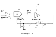
図4は、図2に示した実施例1における測定時の感度調整回路を示す回路構成図である。以下に、測定時の動作について説明する。
Output of VGA = second adjustment voltage VA2
VGA output = first adjustment voltage VA1 × VGA gain VGA gain = second adjustment voltage VA2 / first adjustment voltage VA1
As described above, the VGA gain adjustment voltage VG in which the VGA gain of the
FIG. 4 is a circuit configuration diagram showing a sensitivity adjustment circuit at the time of measurement in the embodiment 1 shown in FIG. The operation during measurement will be described below.
入力切り替えスイッチ13は、入力信号Vinを選択して、VGA11の入力とする。S/H_SW14aはOFFされ、増幅器12の出力と、VGAゲイン調整電圧VGは切断される。そのため、上述した図3で調整されたVGAゲイン調整電圧VGが、接地電圧VSSとの間に接続された容量素子C1によって保持されている。
VGA11は、入力信号電圧VinをVGAゲイン倍して出力し、そのVGAゲインは、容量素子C1によって保持されたVGAゲイン調整電圧VGに応じて決まるため、VGA11の出力信号Voutは、下記の通りとなる。
The
The
出力信号電圧=VGAゲイン×入力信号電圧Vin
=第2調整電圧VA2/第1調整電圧VA1×入力信号電圧Vin
以上の通り、ゲイン調整時に生成したVGAゲイン調整電圧VGを保持しておくことによって、入力信号Vinに対して、VGAゲイン倍(第2調整電圧VA2/第1調整電圧VA1)された出力信号Voutを生成することができる。
この調整では、VGAゲインを決定する際にフィードバックループを組んでいるため、VGA11の非線形性、あるいはVGA11の内部の素子ばらつきなどがあっても、フィードバックループによって、それらも含めてVGAゲイン=第2調整電圧VA2/第1調整電圧VA1となるように調整する。
Output signal voltage = VGA gain x input signal voltage Vin
= Second adjustment voltage VA2 / first adjustment voltage VA1 × input signal voltage Vin
As described above, by holding the VGA gain adjustment voltage VG generated during gain adjustment, the output signal Vout multiplied by VGA gain (second adjustment voltage VA2 / first adjustment voltage VA1) with respect to the input signal Vin. Can be generated.
In this adjustment, since a feedback loop is formed when determining the VGA gain, even if there is a nonlinearity of the
フィードバックループを使ってゲインをVGAゲイン=第2調整電圧VA2/第1調整電圧VA1になるように追い込むため(ゲイン調整時)、感度調整に対して線形性を確保することができる。
また、フィードバックループを切断した後(S/H_SW14aをオフした後)、容量素子C1があることでVGAゲインを一定に保持することができる。それによって、感度調整量に対してVGA11の非線形性、VGA11の素子ばらつきがあっても広範囲に線形性を確保できる。また、感度調整量に対して連続的に補正を行うことができる。
以上は、入力信号Vinに対して、VGAゲイン倍(第2調整電圧VA2/第1調整電圧VA1)された出力信号Voutを生成することができる感度調整回路の実施形態1について説明したが、次に、実施形態2について説明する。
Since the feedback loop is used to drive the gain so that VGA gain = second adjustment voltage VA2 / first adjustment voltage VA1 (during gain adjustment), linearity can be ensured for sensitivity adjustment.
Further, after the feedback loop is cut (after S /
The first embodiment of the sensitivity adjustment circuit that can generate the output signal Vout multiplied by VGA gain (second adjustment voltage VA2 / first adjustment voltage VA1) with respect to the input signal Vin has been described above. Next,
<実施形態2>
図5は、本発明に係る感度調整回路の実施形態2を説明するためのブロック図である。図中符号30は感度調整回路、41は温度センサ、42は電源電圧依存電圧供給回路を示している。
本実施形態2の感度調整回路は、電源電圧変動及び温度変動に対して感度を調整する感度調整回路であって、入力電圧Vinを入力し、出力電圧Voutを出力する感度調整回路30と、この感度調整回路30に温度依存調整電圧VTを供給する温度センサ41と、感度調整回路10に電源電圧依存調整電圧VDを供給する電源電圧依存電圧供給回路42とを備えている。
<
FIG. 5 is a block diagram for explaining a second embodiment of the sensitivity adjustment circuit according to the present invention. In the figure,
The sensitivity adjustment circuit according to the second embodiment is a sensitivity adjustment circuit that adjusts sensitivity to power supply voltage fluctuation and temperature fluctuation. The
つまり、本実施形態2は、実施形態1における第1調整電圧生成回路として温度センサ41を、第2調整電圧生成回路として電源電圧依存電圧供給回路42を備えている。
第1調整電圧は、温度依存調整電圧であり、入力信号Vinに対して温度補正するための電圧である。第2調整電圧は、電源電圧依存調整電圧であり、入力信号Vinに対して電源電圧依存性を持たせるための電圧である。よって、感度調整回路の出力としては、下記の通りとなる。
That is, the second embodiment includes the
The first adjustment voltage is a temperature-dependent adjustment voltage and is a voltage for correcting the temperature of the input signal Vin. The second adjustment voltage is a power supply voltage dependent adjustment voltage, and is a voltage for making the input signal Vin have power supply voltage dependency. Therefore, the output of the sensitivity adjustment circuit is as follows.
出力信号電圧=電源電圧依存調整電圧VD/温度依存調整電圧VT×入力信号電圧
第1調整電圧VA1及び第2調整電圧VA2を、それぞれ温度補正するための温度依存調整電圧VT、電源電圧依存性を持たせるための電源電圧依存調整電圧VDとすることで、入力信号Vinに対して、電源電圧依存性と温度補正を行うことができる。
例えば、入力信号Vinに温度依存性がある場合、温度依存調整電圧VTを、周囲・環境温度に基づく同様の温度依存性を持った電圧とすることで、入力信号Vin/温度依存調整電圧VTによって、温度補正を行うことができることがわかる。
また、入力信号Vinに電源電圧依存性をもたせたい場合、電源電圧依存調整電圧VDを、電源電圧依存性をもった電圧とすることで、入力信号Vin×電源電圧依存調整電圧VDによって、電源電圧依存性をもたせることができることがわかる。
Output signal voltage = Power supply voltage dependent adjustment voltage VD / Temperature dependent adjustment voltage VT × Input signal voltage The first adjustment voltage VA1 and the second adjustment voltage VA2 are temperature-dependent adjustment voltage VT and power supply voltage dependency for temperature correction, respectively. By using the power supply voltage dependent adjustment voltage VD for providing the input signal Vin, the power supply voltage dependency and temperature correction can be performed on the input signal Vin.
For example, when the input signal Vin is temperature-dependent, the temperature-dependent adjustment voltage VT is set to a voltage having the same temperature dependency based on the ambient / environment temperature, so that the input signal Vin / temperature-dependent adjustment voltage VT It can be seen that temperature correction can be performed.
When it is desired to make the input signal Vin dependent on the power supply voltage, the power supply voltage dependent adjustment voltage VD is set to a voltage having the power supply voltage dependence, so that the input signal Vin × the power supply voltage dependent adjustment voltage VD It can be seen that dependency can be given.
図6は、図5に示した実施形態2に基づいた実施例2を説明するための感度調整回路の回路構成図である。図中符号31は可変利得増幅器(VGA;variable gain amplifier)、32は増幅器(amp)、33は入力切替部(SW)、34はサンプル/ホールド部、34aはサンプル/ホールドスイッチ(S/H_SW)を示している。
可変利得増幅器(VGA)31は、利得調整電圧VGに基づいて利得が調整される。入力切替部(SW)33は、可変利得増幅器31に入力する信号を、入力電圧Vinと温度依存調整電圧VTとで切り替える。
FIG. 6 is a circuit configuration diagram of a sensitivity adjustment circuit for explaining Example 2 based on
The gain of the variable gain amplifier (VGA) 31 is adjusted based on the gain adjustment voltage VG. The input switching unit (SW) 33 switches a signal input to the
増幅器32は、可変利得増幅器31の出力電圧Voutと電源電圧依存調整電圧VDが入力される。サンプル/ホールド部34は、サンプル/ホールドを切り替える第1サンプル/ホールドスイッチ(S/H_SW)34aと、第1容量素子C1とを備え、増幅器32の出力をサンプル/ホールドして利得調整電圧を生成する。
このような構成により、利得調整区間では、入力切替部33を切り替えて可変利得増幅器31に温度依存調整電圧VTが入力されて、サンプル/ホールド部34が増幅器32の出力をサンプル/ホールドする。
The
With such a configuration, in the gain adjustment section, the
測定区間では、入力切替部33を切り替えて可変利得増幅器31に入力電圧Vinが入力されて、サンプル/ホールド部34がホールドした利得調整電圧VGに基づいて入力電圧Vinが調整されて出力される。
また、測定区間において、可変利得増幅器31の利得が、電源電圧依存調整電圧VD/温度依存調整電圧VTに比例する利得である。また、測定区間において、入力電圧Vinが、電源電圧依存調整電圧VD/温度依存調整電圧VTに比例する利得で調整されて出力される。
また、サンプル/ホールド部34は、第1容量素子C1とローパスフィルタLPFを形成する第1抵抗素子R1をさらに備えている。
In the measurement section, the
In the measurement section, the gain of the
The sample /
図7は、図6に示した実施例2におけるゲイン調整時の感度調整回路を示す回路構成図である。以下に、感度調整回路30のゲイン調整時の動作について説明する。
入力切り替えスイッチ33は、温度依存調整電圧VTを選択してVGA31の入力とする。S/H_SW34aがONとなり、増幅器32の出力がVGAゲイン調整電圧(コントロール電圧)VGとなる。この時、感度調整回路30で形成されるフィードバックループにより、VGA31の出力が、電源電圧依存調整電圧VDとなるようにVGAゲイン調整電圧VGが決定される。
FIG. 7 is a circuit configuration diagram showing a sensitivity adjustment circuit at the time of gain adjustment in the second embodiment shown in FIG. Hereinafter, an operation at the time of gain adjustment of the
The
具体的には、VGA31の出力が、増幅器32の反転入力端子に入力され、電源電圧依存調整電圧VDが増幅器32の非反転入力端子に入力される。VGA31の出力が、電源電圧依存調整電圧VDよりも高い場合、増幅器32の出力電圧が低下するため、VGAゲイン調整電圧VGが低下する。それによって、VGA31の出力が、電源電圧依存調整電圧VDとなるようにVGAゲイン調整電圧VGが決定される。
そして、VGA31では、入力される温度依存調整電圧VTを、VGAゲイン調整電圧VGに応じたVGAゲイン倍で出力することから、下記の式が成り立つ。
Specifically, the output of the
The
VGAの出力=電源電圧依存調整電圧VD
VGAの出力=温度依存調整電圧VT×VGAゲイン
VGAゲイン=電源電圧依存調整電圧VD/温度依存調整電圧VT
以上の通り、VGA31のVGAゲインが、電源電圧依存調整電圧VD/温度依存調整電圧VTとなるVGAゲイン調整電圧VGを容量素子C1に保持することができる。
VGA output = power supply voltage dependent adjustment voltage VD
VGA output = temperature dependent adjustment voltage VT × VGA gain VGA gain = power supply voltage dependent adjustment voltage VD / temperature dependent adjustment voltage VT
As described above, the VGA gain adjustment voltage VG in which the VGA gain of the
図8は、図6に示した実施例2における測定時の感度調整回路を示す回路構成図である。以下に、測定時の動作について説明する。
入力切り替えスイッチ33は、入力信号Vinを選択して、VGA31の入力とする。S/H_SW34aはOFFされ、増幅器32の出力と、VGAゲイン調整電圧VGは切断される。そのため、上述した図7で調整されたVGAゲイン調整電圧VGが、接地電圧VSSとの間に接続された容量素子C1によって保持されている。
VGA31は、入力信号電圧VinをVGAゲイン倍して出力し、そのVGAゲインは、容量素子C1によって保持されたVGAゲイン調整電圧VGに応じて決まるため、VGA31の出力信号Voutは、下記の通りとなる。
FIG. 8 is a circuit configuration diagram showing a sensitivity adjustment circuit at the time of measurement in the second embodiment shown in FIG. The operation during measurement will be described below.
The
The
出力信号電圧=VGAゲイン×入力信号電圧Vin
=電源電圧依存調整電圧VD/温度依存調整電圧VT×入力信号電圧Vin
以上の通り、ゲイン調整時に生成したVGAゲイン調整電圧VGを保持しておくことによって、入力信号Vinに対して、VGAゲイン倍(電源電圧依存調整電圧VD/温度依存調整電圧VT)された出力信号Voutを生成することができる。
この調整では、VGAゲインを決定する際にフィードバックループを組んでいるため、VGA31の非線形性、あるいはVGA31の内部の素子ばらつきなどがあっても、フィードバックループによって、それらも含めてVGAゲイン=電源電圧依存調整電圧VD/温度依存調整電圧VTとなるように調整する。
Output signal voltage = VGA gain x input signal voltage Vin
= Power supply voltage dependent adjustment voltage VD / Temperature dependent adjustment voltage VT x Input signal voltage Vin
As described above, by holding the VGA gain adjustment voltage VG generated at the time of gain adjustment, the output signal multiplied by VGA gain (power supply voltage dependent adjustment voltage VD / temperature dependent adjustment voltage VT) with respect to the input signal Vin. Vout can be generated.
In this adjustment, a feedback loop is formed when determining the VGA gain. Therefore, even if there is nonlinearity of the
フィードバックループを使ってゲインをVGAゲイン=電源電圧依存調整電圧VD/温度依存調整電圧VTになるように追い込むため(ゲイン調整時)、感度調整に対して線形性を確保することができる。
また、フィードバックループを切断した後(S/H_SW34をオフした後)、容量素子C1があることでVGAゲインを一定に保持することができる。それによって、感度調整量に対してVGA31の非線形性、VGA31の素子ばらつきがあっても広範囲に線形性を確保できる。また、感度調整量に対して連続的に補正を行うことができる。
Since the feedback loop is used to drive the gain so that VGA gain = power supply voltage-dependent adjustment voltage VD / temperature-dependent adjustment voltage VT (at the time of gain adjustment), linearity can be ensured for sensitivity adjustment.
Further, after the feedback loop is cut (after S /
<実施形態3>
本実施形態3の感度調整回路は、異なる2つの調整電圧に対して感度を調整する感度調整回路であって、入力電圧Vinを入力し、出力電圧Voutを出力する感度調整回路と、この感度調整回路に第1調整電圧VA1を供給する第1調整電圧生成回路と、感度調整回路に第2調整電圧VA2を供給する第2調整電圧生成回路とを備えている。つまり、実施形態1と同様な構成を有している。
<
The sensitivity adjustment circuit according to the third embodiment is a sensitivity adjustment circuit that adjusts sensitivity with respect to two different adjustment voltages. The sensitivity adjustment circuit receives an input voltage Vin and outputs an output voltage Vout. The circuit includes a first adjustment voltage generation circuit that supplies a first adjustment voltage VA1 to the circuit, and a second adjustment voltage generation circuit that supplies a second adjustment voltage VA2 to the sensitivity adjustment circuit. That is, it has the same configuration as that of the first embodiment.
そして、感度調整回路は、第1調整電圧VA1と第2調整電圧VA2を基に、入力信号Vinに対する出力信号Voutの感度を調整する。上述した実施形態1との相違は、図9に基づいて後述するが、サンプル/ホールド部54が、サンプル/ホールドを切り替える第1サンプル/ホールドスイッチ54−1乃至54−4と第1容量素子C1及び第2容量素子C2とを備えている点である。
The sensitivity adjustment circuit adjusts the sensitivity of the output signal Vout with respect to the input signal Vin based on the first adjustment voltage VA1 and the second adjustment voltage VA2. Although the difference from the first embodiment will be described later with reference to FIG. 9, the sample /
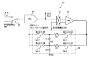
図9は、本発明に係る感度調整回路の実施形態3を説明するためのブロック図である。図中符号50は感度調整回路、51は可変利得増幅器(VGA)、52は増幅器(amp)、53は入力切替部(SW)、54はサンプル/ホールド部、54−1乃至54−4は第1乃至第4サンプル/ホールドスイッチ(S/H_SW)、55は極性切替部を示している。
本実施形態3の感度調整回路は、入力電圧Vinを入力し、出力電圧Voutを出力する感度調整回路50と、この感度調整回路50に第1調整電圧VA1を供給する第1調整電圧生成回路と、感度調整回路50に第2調整電圧VA2を供給する第2調整電圧生成回路とを備えている。
FIG. 9 is a block diagram for explaining a third embodiment of the sensitivity adjustment circuit according to the present invention. In the figure,
The sensitivity adjustment circuit according to the third embodiment includes a
可変利得増幅器51は、利得調整電圧VGに基づいて利得が調整される。入力切替部53は、可変利得増幅器51に入力する信号を、入力電圧Vinと第1調整電圧VA1とで切り替える。
また、増幅器52は、可変利得増幅器51の出力電圧Voutと第2調整電圧VA2が入力される。また、極性切替部55は、増幅器52の入力極性を切り替える。また、サンプル/ホールド部54は、増幅器52の出力をサンプル/ホールドして利得調整電圧を生成する。
The gain of the
The
このような構成により、第1利得調整区間では、可変利得増幅器51に第1調整電圧VA1が入力され、増幅器52に第2調整電圧VA2が入力され、サンプル/ホールド部54が増幅器52の第1出力をサンプル/ホールドする。
また、第2利得調整区間では、可変利得増幅器51に極性が反転した第1調整電圧VA1が入力され、増幅器52に極性が反転した第2調整電圧VA2が入力され、増幅器52の入力極性が切り替えられ、サンプル/ホールド部54が増幅器52の第2出力をサンプル/ホールドする。
With this configuration, in the first gain adjustment section, the first adjustment voltage VA1 is input to the
In the second gain adjustment period, the
測定区間では、可変利得増幅器51に入力電圧Vinが入力されて、サンプル/ホールド部54がホールドした第1出力及び第2出力を平均化した利得調整電圧VGに基づいて入力電圧Vinが調整されて出力される。
また、サンプル/ホールド部54は、第1調整区間でサンプル/ホールドを切り替える、第1サンプル/ホールドスイッチ54−1と第2サンプル/ホールドスイッチ54−2及び第1容量素子C1とを備え、また、第2調整区間でサンプル/ホールドを切り替える、第3サンプル/ホールドスイッチ54−3と第4サンプル/ホールドスイッチ54−4及び第2容量素子C2とを備えている。
In the measurement period, the input voltage Vin is input to the
The sample /
可変利得増幅器51と増幅器52との間に、第2サンプル/ホールドスイッチ54−2と第1容量素子C1と第1抵抗素子R1と第1サンプル/ホールドスイッチ54−1とが順次接続され、これに並列に、第4サンプル/ホールドスイッチ54−4と第2容量素子C2と第2抵抗素子R2と第3サンプル/ホールドスイッチ54−3とが順次接続されている。
また、第1調整区間では、第1サンプル/ホールドスイッチ54−1と第2サンプル/ホールドスイッチ54−2とで、第1容量素子C1に増幅器52の第1出力をサンプル/ホールドし、第2調整区間では、第3サンプル/ホールドスイッチ54−3と第4サンプル/ホールドスイッチ54−4とで、第2容量素子C2に増幅器52の第2出力をサンプル/ホールドする。
Between the
In the first adjustment period, the first sample / hold switch 54-1 and the second sample / hold switch 54-2 sample / hold the first output of the
測定区間では、第2サンプル/ホールドスイッチ54−2と第4サンプル/ホールドスイッチ54−4で、第1容量素子C1及び第2容量素子C2がホールドした第1出力及び第2出力を平均化して利得調整電圧VGを生成する。
また、第1調整電圧生成回路と、第2調整電圧生成回路とを備え、第1調整電圧生成回路は、第1調整区間では、第1調整電圧VA1を生成し、第2調整区間では、極性が反転した第1調整電圧VA1を生成する。第2調整電圧生成回路は、第1調整区間では、第2調整電圧VA2を生成し、第2調整区間では、極性が反転した第2調整電圧VA2を生成する。
In the measurement period, the first output and the second output held by the first capacitive element C1 and the second capacitive element C2 are averaged by the second sample / hold switch 54-2 and the fourth sample / hold switch 54-4. A gain adjustment voltage VG is generated.
The first adjustment voltage generation circuit includes a first adjustment voltage generation circuit and a second adjustment voltage generation circuit. The first adjustment voltage generation circuit generates the first adjustment voltage VA1 in the first adjustment section, and the polarity in the second adjustment section. The first adjustment voltage VA1 is generated by inverting. The second adjustment voltage generation circuit generates the second adjustment voltage VA2 in the first adjustment section, and generates the second adjustment voltage VA2 whose polarity is inverted in the second adjustment section.
例えば、第1調整電圧VA1は、温度依存電圧であり、第2調整電圧VA2は、電源電圧依存電圧として調整を行うことができる。
つまり、本実施形態3の感度調整回路50は、可変利得増幅回路(VGA)51と増幅器52と切り替えスイッチ53とサンプル/ホールド部54とを備えている。サンプル/ホールド部54は、第1S/Hスイッチ(サンプル/ホールドスイッチ)54−1と第2S/Hスイッチ(サンプル/ホールドスイッチ)54−2と第3S/Hスイッチ(サンプル/ホールドスイッチ)54−3と第4S/Hスイッチ(サンプル/ホールドスイッチ)54−4とを備えている。
For example, the first adjustment voltage VA1 can be adjusted as a temperature-dependent voltage, and the second adjustment voltage VA2 can be adjusted as a power supply voltage-dependent voltage.
That is, the
さらに、電圧を保持するための第1容量素子C1と第2容量素子C2、増幅器52のノイズを低減するための第1容量素子C1とフィルタを形成する第1抵抗素子R1、第2容量素子C2とフィルタを形成する第2抵抗素子R2とを備えている。また、増幅器52に接続され、入力極性を切り替える極性切替部(SW)55を備えている。
本実施形態3は、VGA51から生じる、特に、低周波の1/fノイズを低減するために、ゲイン調整時において極性切替してサンプル/ホールドを行うものである。以下に、具体的な動作について説明する。
Furthermore, the first capacitor element C1 and the second capacitor element C2 for holding the voltage, the first capacitor element C1 for reducing the noise of the
In the third embodiment, in order to reduce the low frequency 1 / f noise generated from the
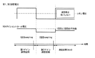
図10は、図9に示した感度調整回路の動作を説明するためのタイミングチャートを示す図である。この図10に示すように時間軸において3つの状態、つまり、第1ゲイン調整区間と第2ゲイン調整区間と測定区間との3つの状態を繰り返している。
まず、上述した感度調整回路(ゲイン調整時)の説明と同様で、ゲイン調整1回目の動作を行い、その結果をサンプリングしホールドする。
次に、第1調整電圧及び第2調整電圧を反転しゲイン調整2回目を行う、その際ゲイン調整1回目の結果は、ホールド状態のまま、第1容量素子C1に保持されている。
最後の測定動作時では、ゲイン調整で2回行ったサンプリング結果を平均化してホールドし、VGAゲイン調整電圧とする。以下、各動作について具体的に説明する。
FIG. 10 is a timing chart for explaining the operation of the sensitivity adjustment circuit shown in FIG. As shown in FIG. 10, three states on the time axis, that is, three states of the first gain adjustment section, the second gain adjustment section, and the measurement section are repeated.
First, similarly to the description of the sensitivity adjustment circuit (at the time of gain adjustment), the first gain adjustment operation is performed, and the result is sampled and held.
Next, the first adjustment voltage and the second adjustment voltage are inverted and the second gain adjustment is performed. At this time, the result of the first gain adjustment is held in the first capacitive element C1 while being held.
At the time of the last measurement operation, the sampling results obtained twice by gain adjustment are averaged and held to obtain a VGA gain adjustment voltage. Each operation will be specifically described below.
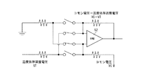
図11は、図9に示した実施例3におけるゲイン調整時(1回目)の感度調整回路を示す回路構成図である。まず、感度調整回路50のゲイン調整時の動作について説明する。以下に1回目のゲイン調整時について説明する。
入力切り替えスイッチ53は、第1調整電圧(コモン電圧VC+第1調整電圧VA1)を選択してVGA51の入力とする。なお、この1回目調整時では、VGA51に入力する第1調整電圧として、コモン電圧VCに対して正転の第1調整電圧(+第1調整電圧VA1)とする。
FIG. 11 is a circuit configuration diagram showing a sensitivity adjustment circuit at the time of gain adjustment (first time) in the third embodiment shown in FIG. First, the operation at the time of gain adjustment of the
The
第1S/Hスイッチ54−1と第2S/Hスイッチ54−2はONであり、第1のフィードバックループが形成され、増幅器52の出力がVGAゲイン調整電圧となる。また、第3S/Hスイッチ54−3と第4S/Hスイッチ54−4はOFFであり、第2のフィードバックループは形成されていない。
この時、感度調整回路50で形成される第1のフィードバックループにより、VGA51の出力が、第2調整電圧である、コモン電圧VCに対して正転の第2調整電圧(+第2調整電圧VA2)となるように、VGAゲイン調整電圧が決定される。そして、VGA51では、入力される第1調整電圧(コモン電圧VCに対して+第1調整電圧VA1)を、VGAゲイン調整電圧に応じたVGAゲイン倍で出力することから、下記の式が成り立つ。
The first S / H switch 54-1 and the second S / H switch 54-2 are ON, a first feedback loop is formed, and the output of the
At this time, due to the first feedback loop formed by the
VGA出力=コモン電圧VCに対して+第2調整電圧VA2
VGA出力=コモン電圧VCに対して+第1調整電圧VA1×VGAゲイン
VGAゲイン=(+第2調整電圧VA2)/(+第1調整電圧VA1)
以上の通り、VGA51のVGAゲインが、(+第2調整電圧VA2)/(+第1調整電圧VA1)となるVGAゲイン調整電圧を第1容量素子C1に保持することができる。
VGA output = common voltage VC + second adjustment voltage VA2
VGA output = common voltage VC + first adjustment voltage VA1 × VGA gain VGA gain = (+ second adjustment voltage VA2) / (+ first adjustment voltage VA1)
As described above, the VGA gain adjustment voltage at which the VGA gain of the
図12は、図9に示した実施例3におけるゲイン調整時(2回目)の感度調整回路を示す回路構成図である。以下に、2回目のゲイン調整時について説明する。
入力切り替えスイッチ53は、第1調整電圧(コモン電圧VC−第1調整電圧VA1)を選択してVGA51の入力とする。なお、この2回目調整時では、VGA51に入力する第1調整電圧として、コモン電圧VCに対して反転の第1調整電圧(−第1調整電圧VA1)とする。
第3S/Hスイッチ54−3と第4S/Hスイッチ54−4はONであり、第2のフィードバックループが形成され、増幅器52の出力がVGAゲイン調整電圧となる。また、第1S/Hスイッチ54−1と第2S/Hスイッチ54−2はOFFであり、第1のフィードバックループは形成されていない。
FIG. 12 is a circuit configuration diagram showing a sensitivity adjustment circuit at the time of gain adjustment (second time) in the third embodiment shown in FIG. The second gain adjustment will be described below.
The
The third S / H switch 54-3 and the fourth S / H switch 54-4 are ON, a second feedback loop is formed, and the output of the
このとき、第1容量素子C1は、1回目のゲイン調整時のVGAゲイン調整電圧を保持する。極性切替により、増幅器52の入力の極性を、ゲイン調整時1回目から反転させる。
この時、感度調整回路50で形成される第2のフィードバックループにより、VGA51の出力が、第2調整電圧である、コモン電圧VCに対して反転の第2調整電圧(−第2調整電圧VA2)となるように、VGAゲイン調整電圧が決定される。そして、VGA51では、入力される第1調整電圧(コモン電圧VCに対して−第1調整電圧VA1)を、VGAゲイン調整電圧に応じたVGAゲイン倍で出力することから、下記の式が成り立つ。
At this time, the first capacitive element C1 holds the VGA gain adjustment voltage at the time of the first gain adjustment. By switching the polarity, the polarity of the input of the
At this time, by the second feedback loop formed by the
VGA出力=コモン電圧VCに対して−第2調整電圧VA2
VGA出力=コモン電圧VCに対して−第1調整電圧VA1×VGAゲイン
VGAゲイン=(−第2調整電圧VA2)/(−第1調整電圧VA1)
以上の通り、VGA51のVGAゲインが、(−第2調整電圧VA2)/(−第1調整電圧VA1)となるVGAゲイン調整電圧を第2容量素子C2に保持することができる。
VGA output = common voltage VC−second adjustment voltage VA2
VGA output = common voltage VC−first adjustment voltage VA1 × VGA gain VGA gain = (− second adjustment voltage VA2) / (− first adjustment voltage VA1)
As described above, the VGA gain adjustment voltage at which the VGA gain of the
図13は、図9に示した実施例3における測定時の感度調整回路を示す回路構成図である。以下に、測定時の動作について説明する。
入力切り替えスイッチ53は、入力信号を選択してVGA51の入力とする。
第1S/Hスイッチ54−1と第3S/Hスイッチ54−3はOFFとなり、増幅器52の出力とVGAゲイン調整電圧は切断される。
また、第2S/Hスイッチ54−2と第4S/Hスイッチ54−4はONとなり、第1容量素子C1に保持されたVGAゲイン調整電圧と、第2容量素子C2に保持されたVGAゲイン調整電圧の平均値となるように、VGAゲインが決定され、その平均した電圧が、接地電圧VSSとの間に接続された第1容量素子C1及び第2容量素子C2によって保持される。出力信号電圧=VGAゲイン×入力信号電圧である。
FIG. 13 is a circuit configuration diagram showing a sensitivity adjustment circuit at the time of measurement in the third embodiment shown in FIG. The operation during measurement will be described below.
The
The first S / H switch 54-1 and the third S / H switch 54-3 are turned OFF, and the output of the
Further, the second S / H switch 54-2 and the fourth S / H switch 54-4 are turned on, and the VGA gain adjustment voltage held in the first capacitor element C1 and the VGA gain adjustment held in the second capacitor element C2. The VGA gain is determined so as to be an average value of the voltage, and the averaged voltage is held by the first capacitor element C1 and the second capacitor element C2 connected to the ground voltage VSS. Output signal voltage = VGA gain × input signal voltage.
このとき、図10及び図11で調整されたVGAゲイン調整電圧が、接地電圧VSSとの間に接続された第1容量素子C1及び第2容量素子C2によって保持されているため、
VGAゲイン=((+第2調整電圧VA2)/(+第1調整電圧VA1)+(−第2調整電圧VA2)/(−第1調整電圧VA1))/2=(第2調整電圧VA2)/(第1調整電圧VA1)
結局、出力信号電圧=(第2調整電圧VA2)/(第1調整電圧VA1)×入力信号電圧となる。
At this time, the VGA gain adjustment voltage adjusted in FIGS. 10 and 11 is held by the first capacitor element C1 and the second capacitor element C2 connected to the ground voltage VSS.
VGA gain = ((+ second adjustment voltage VA2) / (+ first adjustment voltage VA1) + (− second adjustment voltage VA2) / (− first adjustment voltage VA1)) / 2 = (second adjustment voltage VA2) / (First adjustment voltage VA1)
Eventually, output signal voltage = (second adjustment voltage VA2) / (first adjustment voltage VA1) × input signal voltage.
本実施形態3の動作概要に示したようなサンプルホールド動作を行うことによって、VGA51から生じるフリッカーノイズに対して、(Z−1−1)/2の伝達関数で示されるフィルタがかかることとなる。
上述した通り、ゲイン調整時1回目とゲイン調整時2回目で、各容量素子に保持されたVGAゲイン調整電圧が、測定時に平均化されることによって、ゲイン調整時1回目と2回目でVGAから生じるフリッカーノイズが(Z−1−1)/2の伝達関数で示されるハイパスフィルタで除去されることとなる。
By performing the sample and hold operation as shown in the operation outline of the third embodiment, a filter represented by a transfer function of (Z −1 −1) / 2 is applied to the flicker noise generated from the
As described above, the VGA gain adjustment voltage held in each capacitor element is averaged during measurement at the first gain adjustment and the second gain adjustment, so that the VGA gain adjustment voltage is obtained from the VGA at the first and second gain adjustment. The generated flicker noise is removed by a high-pass filter represented by a transfer function of (Z −1 −1) / 2.
ここで、Zは、Z変換によるものであり、ゲイン調整時1回目と2回目のサンプリング時間に関連する。
VGA51から生じる低帯域のフリッカーノイズ(1/fノイズ)については、上述したサンプル/ホールド動作を行うことによって、測定時には、疑似的なハイパスフィルタによって、VGA出力が除去されることとなる。これによって、調整回路の出力信号におけるノイズ成分を低減することができるのである。
Here, Z is due to Z conversion, and is related to the first and second sampling times during gain adjustment.
For the low-band flicker noise (1 / f noise) generated from the
図14は、図11に示した第1調整電圧を温度依存調整電圧としたときの本実施形態3におけるコモン電圧に対する+温度依存調整電圧(ゲイン調整1回目)を生成する回路図である。
図15は、図11に示した第1調整電圧を温度依存調整電圧としたときの本実施形態3におけるコモン電圧に対する−温度依存調整電圧(ゲイン調整2回目)を生成する回路図である。
ゲイン調整1回目では、図14に示すように、温度依存調整電圧とコモン電圧が抵抗分割された電圧が増幅器52の非反転入力端子に入力され、接地電圧VSSと増幅器52の出力が抵抗分割された電圧が増幅器52の反転入力端子に入力される。このとき、増幅器52の出力は、コモン電圧に対して+温度依存調整電圧となる。
一方、ゲイン調整2回目では、図15に示すように、温度依存調整電圧と増幅器52の出力が抵抗分割された電圧が増幅器52の反転入力端子に入力され、接地電圧VSSとコモン電圧が抵抗分割された電圧が増幅器52のも非反転入力端子に入力される。このとき、増幅器52の出力は、コモン電圧に対して−温度依存調整電圧となる。
FIG. 14 is a circuit diagram for generating a + temperature-dependent adjustment voltage (first gain adjustment) for the common voltage in the third embodiment when the first adjustment voltage shown in FIG. 11 is a temperature-dependent adjustment voltage.
FIG. 15 is a circuit diagram for generating a −temperature dependent adjustment voltage (second gain adjustment) for the common voltage in the third embodiment when the first adjustment voltage shown in FIG. 11 is a temperature dependent adjustment voltage.
In the first gain adjustment, as shown in FIG. 14, a voltage obtained by resistance-dividing the temperature-dependent adjustment voltage and the common voltage is input to the non-inverting input terminal of the
On the other hand, in the second gain adjustment, as shown in FIG. 15, the temperature-dependent adjustment voltage and the voltage obtained by resistance-dividing the output of the
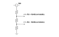
図16は、第2調整電圧を電源電圧依存調整電圧としたときの本実施形態3におけるコモン電圧に対する±電源電圧依存調整電圧を生成する回路図である。電源から抵抗素子による電圧分割により生成している。
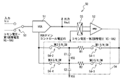
図17は、本発明の感度調整回路の使用例の一例を示す回路構成図で、圧力センサからの出力信号を、回路で補正、増幅などして出力する回路図である。図17に示すG1段、G2段、G3段では、圧力センサからの出力信号を増幅、オフセット補正及びセンサの感度ばらつきの補正を行っている。補正された出力を、サンプルホールド動作し、バッファから出力している。
FIG. 16 is a circuit diagram for generating a ± power supply voltage dependent adjustment voltage with respect to the common voltage in the third embodiment when the second adjustment voltage is a power supply voltage dependent adjustment voltage. It is generated from the power supply by voltage division by a resistance element.
FIG. 17 is a circuit configuration diagram showing an example of use of the sensitivity adjustment circuit of the present invention, and is a circuit diagram for outputting an output signal from the pressure sensor after correcting and amplifying the signal by the circuit. In the G1, G2, and G3 stages shown in FIG. 17, the output signal from the pressure sensor is amplified, offset correction, and sensor sensitivity variation correction are performed. The corrected output is sampled and held and output from the buffer.
本発明の感度調整回路は、センサの温度感度を補正し、出力に電源電圧依存性を持たせるために使用されている。
感度調整回路の入力は、具体例に示したように第1調整電圧供給手段として温度センサを、第2調整電圧供給手段として電源電圧に依存する電圧を供給する回路を使用している。温度変動に対して感度調整回路でゲインを調整することでセンサ感度の温度変動に対して、補正を行い、出力を一定に保つ回路となっている。また、電源電圧に比例した出力になる回路となっている。
The sensitivity adjustment circuit of the present invention is used to correct the temperature sensitivity of the sensor and to make the output dependent on the power supply voltage.
As shown in the specific example, the input of the sensitivity adjustment circuit uses a temperature sensor as the first adjustment voltage supply means and a circuit that supplies a voltage depending on the power supply voltage as the second adjustment voltage supply means. By adjusting the gain with respect to the temperature fluctuation by the sensitivity adjustment circuit, the temperature fluctuation of the sensor sensitivity is corrected and the output is kept constant. In addition, the circuit has an output proportional to the power supply voltage.
図18は、本発明の感度調整回路の使用例示す回路構成図で、圧力センサからの信号をチョッパスイッチでチョッパ周波数に変調し、その入力信号に対して、感度調整回路で感度調整などを行い、後段で復調する形態を示す回路図である。
この場合、例えば、感度調整回路のVGAから生じる低周波領域の1/fノイズと、センサ入力信号とを周波数帯域で分離することができるため、好適である。
FIG. 18 is a circuit configuration diagram showing an example of use of the sensitivity adjustment circuit of the present invention. A signal from a pressure sensor is modulated to a chopper frequency by a chopper switch, and sensitivity adjustment is performed on the input signal by a sensitivity adjustment circuit. FIG. 3 is a circuit diagram showing a form of demodulation in a subsequent stage.
In this case, for example, 1 / f noise in the low frequency region generated from the VGA of the sensitivity adjustment circuit and the sensor input signal can be separated in the frequency band, which is preferable.
1 温度センサ
2 電源
3 マイコン
4 感度調整回路
5 入力端子
6 出力端子
7,8 アナログディジタル変換器(ADC)
9 ディジタルアナログ変換器(DAC)
10,30,50 感度調整回路
21 第1調整電圧生成回路
22 第2調整電圧生成回路
11,31,51 可変利得増幅器(VGA)
12,32,52 増幅器(amp)
13,33,53 入力切替部(SW)
14,34,54 サンプル/ホールド部
14a,34a サンプル/ホールドスイッチ(S/H_SW)
41 温度センサ
42 電源電圧依存電圧供給回路
54−1乃至54−4 第1乃至第4サンプル/ホールドスイッチ
55 極性切替部
1
9 Digital-to-analog converter (DAC)
10, 30, 50
12, 32, 52 Amplifier (amp)
13, 33, 53 Input switching unit (SW)
14, 34, 54 Sample /
41
Claims (12)
前記可変利得増幅器に入力する信号を、入力電圧と第1調整電圧とで切り替える入力切替部と、
前記可変利得増幅器の出力電圧と第2調整電圧が入力される増幅器と、
前記増幅器の出力をサンプル/ホールドして利得調整電圧を生成するサンプル/ホールド部とを備え、
利得調整区間では、前記入力切替部を切り替えて前記可変利得増幅器に前記第1調整電圧が入力されて、前記サンプル/ホールド部が前記増幅器の出力をサンプル/ホールドし、
測定区間では、前記入力切替部を切り替えて前記可変利得増幅器に前記入力電圧が入力されて、前記サンプル/ホールド部がホールドした前記利得調整電圧に基づいて入力電圧が調整されて出力されることを特徴とする感度調整回路。 A variable gain amplifier whose gain is adjusted based on a gain adjustment voltage;
An input switching unit that switches a signal input to the variable gain amplifier between an input voltage and a first adjustment voltage;
An amplifier to which an output voltage of the variable gain amplifier and a second adjustment voltage are input;
A sample / hold unit that samples / holds the output of the amplifier to generate a gain adjustment voltage;
In the gain adjustment interval, the input switching unit is switched to input the first adjustment voltage to the variable gain amplifier, and the sample / hold unit samples / holds the output of the amplifier,
In the measurement period, the input switching unit is switched to input the input voltage to the variable gain amplifier, and the input voltage is adjusted and output based on the gain adjustment voltage held by the sample / hold unit. A characteristic sensitivity adjustment circuit.
前記可変利得増幅器に入力する信号を、入力電圧と第1調整電圧とで切り替える入力切替部と、
前記可変利得増幅器の出力電圧と第2調整電圧が入力される増幅器と、
前記増幅器の入力極性を切り替える極性切替部と、
前記増幅器の出力をサンプル/ホールドして利得調整電圧を生成するサンプル/ホールド部とを備え、
第1利得調整区間では、前記可変利得増幅器に前記第1調整電圧が入力され、前記増幅器に第2調整電圧が入力され、前記サンプル/ホールド部が前記増幅器の第1出力をサンプル/ホールドし、
第2利得調整区間では、前記可変利得増幅器に極性が反転した前記第1調整電圧が入力され、前記増幅器に極性が反転した第2調整電圧が入力され、前記増幅器の入力極性が切り替えられ、前記サンプル/ホールド部が前記増幅器の第2出力をサンプル/ホールドし、
測定区間では、前記可変利得増幅器に前記入力電圧が入力されて、前記サンプル/ホールド部がホールドした前記第1出力及び第2出力を平均化した利得調整電圧に基づいて入力電圧が調整されて出力されることを特徴とする感度調整回路。 A variable gain amplifier whose gain is adjusted based on a gain adjustment voltage;
An input switching unit that switches a signal input to the variable gain amplifier between an input voltage and a first adjustment voltage;
An amplifier to which an output voltage of the variable gain amplifier and a second adjustment voltage are input;
A polarity switching unit for switching the input polarity of the amplifier;
A sample / hold unit that samples / holds the output of the amplifier to generate a gain adjustment voltage;
In the first gain adjustment period, the first adjustment voltage is input to the variable gain amplifier, the second adjustment voltage is input to the amplifier, and the sample / hold unit samples / holds the first output of the amplifier,
In the second gain adjustment period, the variable gain amplifier is supplied with the first adjustment voltage with the polarity reversed, the amplifier is supplied with the second adjustment voltage with the polarity reversed, the input polarity of the amplifier is switched, A sample / hold section samples / holds the second output of the amplifier;
In the measurement period, the input voltage is input to the variable gain amplifier, and the input voltage is adjusted based on the gain adjustment voltage obtained by averaging the first output and the second output held by the sample / hold unit. A sensitivity adjustment circuit.
前記第1調整区間でサンプル/ホールドを切り替える、第1サンプル/ホールドスイッチと第2サンプル/ホールドスイッチ及び第1容量素子と、
前記第2調整区間でサンプル/ホールドを切り替える、第3サンプル/ホールドスイッチと第4サンプル/ホールドスイッチ及び第2容量素子と
を備えていることを特徴とする請求項8に記載の感度調整回路。 The sample / hold unit is
A first sample / hold switch, a second sample / hold switch, and a first capacitive element that switch the sample / hold in the first adjustment interval;
The sensitivity adjustment circuit according to claim 8, further comprising: a third sample / hold switch, a fourth sample / hold switch, and a second capacitance element that switch the sample / hold in the second adjustment section.
前記第2調整区間では、第3サンプル/ホールドスイッチと第4サンプル/ホールドスイッチとで、第2容量素子に前記増幅器の第2出力をサンプル/ホールドし、
前記測定区間では、第2サンプル/ホールドスイッチと第4サンプル/ホールドスイッチで、前記第1容量素子及び前記第2容量素子がホールドした前記第1出力及び第2出力を平均化して利得調整電圧を生成することを特徴とする請求項8又は9に記載の感度調整回路。 In the first adjustment section, the first sample / hold switch and the second sample / hold switch sample / hold the first output of the amplifier to the first capacitive element,
In the second adjustment section, the third sample / hold switch and the fourth sample / hold switch sample / hold the second output of the amplifier to the second capacitance element,
In the measurement period, the second sample / hold switch and the fourth sample / hold switch average the first output and the second output held by the first capacitive element and the second capacitive element to obtain a gain adjustment voltage. 10. The sensitivity adjustment circuit according to claim 8, wherein the sensitivity adjustment circuit is generated.
前記第1調整電圧生成回路は、第1調整区間では、第1調整電圧を生成し、第2調整区間では、極性が反転した第1調整電圧を生成し、
前記第2調整電圧生成回路は、第1調整区間では、第2調整電圧を生成し、第2調整区間では、極性が反転した第2調整電圧を生成することを特徴とする請求項8,9又は10に記載の感度調整回路。 A first adjustment voltage generation circuit; and a second adjustment voltage generation circuit.
The first adjustment voltage generation circuit generates a first adjustment voltage in the first adjustment section, and generates a first adjustment voltage having a reversed polarity in the second adjustment section,
10. The second adjustment voltage generation circuit generates a second adjustment voltage in the first adjustment section, and generates a second adjustment voltage having a reversed polarity in the second adjustment section. Or the sensitivity adjustment circuit of 10.
Priority Applications (1)
| Application Number | Priority Date | Filing Date | Title |
|---|---|---|---|
| JP2014027800A JP2015154352A (en) | 2014-02-17 | 2014-02-17 | sensitivity adjustment circuit |
Applications Claiming Priority (1)
| Application Number | Priority Date | Filing Date | Title |
|---|---|---|---|
| JP2014027800A JP2015154352A (en) | 2014-02-17 | 2014-02-17 | sensitivity adjustment circuit |
Publications (1)
| Publication Number | Publication Date |
|---|---|
| JP2015154352A true JP2015154352A (en) | 2015-08-24 |
Family
ID=53896175
Family Applications (1)
| Application Number | Title | Priority Date | Filing Date |
|---|---|---|---|
| JP2014027800A Pending JP2015154352A (en) | 2014-02-17 | 2014-02-17 | sensitivity adjustment circuit |
Country Status (1)
| Country | Link |
|---|---|
| JP (1) | JP2015154352A (en) |
Cited By (2)
| Publication number | Priority date | Publication date | Assignee | Title |
|---|---|---|---|---|
| CN108904130A (en) * | 2018-07-13 | 2018-11-30 | 上海东软载波微电子有限公司 | Welding mirror |
| JP2019082701A (en) * | 2015-12-01 | 2019-05-30 | エルジー ディスプレイ カンパニー リミテッド | Current integrator and organic light-emitting display device |
-
2014
- 2014-02-17 JP JP2014027800A patent/JP2015154352A/en active Pending
Cited By (3)
| Publication number | Priority date | Publication date | Assignee | Title |
|---|---|---|---|---|
| JP2019082701A (en) * | 2015-12-01 | 2019-05-30 | エルジー ディスプレイ カンパニー リミテッド | Current integrator and organic light-emitting display device |
| CN108904130A (en) * | 2018-07-13 | 2018-11-30 | 上海东软载波微电子有限公司 | Welding mirror |
| CN108904130B (en) * | 2018-07-13 | 2023-12-19 | 上海东软载波微电子有限公司 | Electric welding mirror |
Similar Documents
| Publication | Publication Date | Title |
|---|---|---|
| CN103312328B (en) | Analog-digital converter (ADC) and correcting circuit and its bearing calibration | |
| EP2198313B1 (en) | Switched capacitor measurement circuit for measuring the capacitance of an input capacitor | |
| US9344104B1 (en) | Digital to analog converter and analog to digital converter calibration techniques | |
| JP6346523B2 (en) | Semiconductor integrated circuit and image sensor | |
| JP2010035140A (en) | Analog-to-digital converter | |
| JP6054732B2 (en) | Semiconductor device and offset voltage correction method | |
| US10840866B2 (en) | Amplifier circuit arrangement and method to calibrate the same | |
| JP6313036B2 (en) | Magnetic detector | |
| TWI559115B (en) | Energy gap reference circuit | |
| JP2015154352A (en) | sensitivity adjustment circuit | |
| JP2001044770A (en) | Amplifier circuit | |
| KR20210090166A (en) | PWM modulator with chopping triangle wave PWM quantizer and quantizer with controllable analog gain and correctable for characteristics affecting multi-non-ideal gains | |
| US20090195533A1 (en) | High-accuracy multi-channel circuit | |
| US9171188B2 (en) | Charge measurement | |
| JP5348389B2 (en) | oscilloscope | |
| JP6314681B2 (en) | A / D conversion data correction system for exhaust gas sensor | |
| KR102292597B1 (en) | Automatic offset adjustment appartus for adjusting offset signal of resistive flow sensor | |
| JP2006222701A (en) | Output correction circuit for a/d converter | |
| JP5205942B2 (en) | Zero point correction circuit | |
| JP2016090379A (en) | measuring device | |
| US11012086B2 (en) | Analog-to-digital converter for converting analog signals input from a plurality of sensors | |
| JP2003060504A (en) | A/d conversion apparatus and error correction device for a/d converter | |
| JP2004320553A (en) | Compensating circuit | |
| JP4985972B2 (en) | amplifier | |
| JP2002185329A (en) | Σδ ad converter |