JP2015143846A - Display device and electronic device - Google Patents
Display device and electronic device Download PDFInfo
- Publication number
- JP2015143846A JP2015143846A JP2014258752A JP2014258752A JP2015143846A JP 2015143846 A JP2015143846 A JP 2015143846A JP 2014258752 A JP2014258752 A JP 2014258752A JP 2014258752 A JP2014258752 A JP 2014258752A JP 2015143846 A JP2015143846 A JP 2015143846A
- Authority
- JP
- Japan
- Prior art keywords
- substrate
- display device
- layer
- light
- display
- Prior art date
- Legal status (The legal status is an assumption and is not a legal conclusion. Google has not performed a legal analysis and makes no representation as to the accuracy of the status listed.)
- Withdrawn
Links
- 239000000758 substrate Substances 0.000 claims abstract description 357
- 239000003365 glass fiber Substances 0.000 claims abstract description 93
- 239000004065 semiconductor Substances 0.000 claims description 73
- 230000015572 biosynthetic process Effects 0.000 claims description 53
- 229920002379 silicone rubber Polymers 0.000 claims description 6
- 239000004945 silicone rubber Substances 0.000 claims description 6
- 239000010410 layer Substances 0.000 description 392
- 239000010408 film Substances 0.000 description 100
- 238000000034 method Methods 0.000 description 90
- 239000000463 material Substances 0.000 description 55
- 239000012790 adhesive layer Substances 0.000 description 45
- 230000006870 function Effects 0.000 description 35
- IJGRMHOSHXDMSA-UHFFFAOYSA-N Atomic nitrogen Chemical compound N#N IJGRMHOSHXDMSA-UHFFFAOYSA-N 0.000 description 30
- 150000004767 nitrides Chemical class 0.000 description 27
- 238000004519 manufacturing process Methods 0.000 description 26
- 239000004973 liquid crystal related substance Substances 0.000 description 24
- 229920005989 resin Polymers 0.000 description 23
- 239000011347 resin Substances 0.000 description 23
- 229910052751 metal Inorganic materials 0.000 description 22
- 229910052721 tungsten Inorganic materials 0.000 description 21
- 239000010937 tungsten Substances 0.000 description 21
- 229910052782 aluminium Inorganic materials 0.000 description 20
- XAGFODPZIPBFFR-UHFFFAOYSA-N aluminium Chemical compound [Al] XAGFODPZIPBFFR-UHFFFAOYSA-N 0.000 description 20
- 239000002184 metal Substances 0.000 description 20
- 239000000126 substance Substances 0.000 description 20
- WFKWXMTUELFFGS-UHFFFAOYSA-N tungsten Chemical compound [W] WFKWXMTUELFFGS-UHFFFAOYSA-N 0.000 description 20
- 239000000835 fiber Substances 0.000 description 18
- RTAQQCXQSZGOHL-UHFFFAOYSA-N Titanium Chemical compound [Ti] RTAQQCXQSZGOHL-UHFFFAOYSA-N 0.000 description 16
- 229910052719 titanium Inorganic materials 0.000 description 16
- 239000010936 titanium Substances 0.000 description 16
- 229910052581 Si3N4 Inorganic materials 0.000 description 15
- 229910052757 nitrogen Inorganic materials 0.000 description 15
- HQVNEWCFYHHQES-UHFFFAOYSA-N silicon nitride Chemical compound N12[Si]34N5[Si]62N3[Si]51N64 HQVNEWCFYHHQES-UHFFFAOYSA-N 0.000 description 15
- 239000012535 impurity Substances 0.000 description 14
- 238000000926 separation method Methods 0.000 description 14
- XUIMIQQOPSSXEZ-UHFFFAOYSA-N Silicon Chemical compound [Si] XUIMIQQOPSSXEZ-UHFFFAOYSA-N 0.000 description 13
- 239000004020 conductor Substances 0.000 description 13
- 239000007789 gas Substances 0.000 description 13
- 239000012212 insulator Substances 0.000 description 13
- 230000007935 neutral effect Effects 0.000 description 13
- 229910052710 silicon Inorganic materials 0.000 description 13
- 239000010703 silicon Substances 0.000 description 13
- 238000005452 bending Methods 0.000 description 12
- 239000001257 hydrogen Substances 0.000 description 12
- 229910052739 hydrogen Inorganic materials 0.000 description 12
- 239000002356 single layer Substances 0.000 description 12
- ZOKXTWBITQBERF-UHFFFAOYSA-N Molybdenum Chemical compound [Mo] ZOKXTWBITQBERF-UHFFFAOYSA-N 0.000 description 11
- 239000003990 capacitor Substances 0.000 description 11
- AMGQUBHHOARCQH-UHFFFAOYSA-N indium;oxotin Chemical compound [In].[Sn]=O AMGQUBHHOARCQH-UHFFFAOYSA-N 0.000 description 11
- 229910052750 molybdenum Inorganic materials 0.000 description 11
- 239000011733 molybdenum Substances 0.000 description 11
- VYPSYNLAJGMNEJ-UHFFFAOYSA-N silicon dioxide Inorganic materials O=[Si]=O VYPSYNLAJGMNEJ-UHFFFAOYSA-N 0.000 description 11
- RYGMFSIKBFXOCR-UHFFFAOYSA-N Copper Chemical compound [Cu] RYGMFSIKBFXOCR-UHFFFAOYSA-N 0.000 description 10
- 239000000956 alloy Substances 0.000 description 10
- 230000000903 blocking effect Effects 0.000 description 10
- 229910052802 copper Inorganic materials 0.000 description 10
- 239000010949 copper Substances 0.000 description 10
- 230000007547 defect Effects 0.000 description 10
- 238000005530 etching Methods 0.000 description 10
- 239000011521 glass Substances 0.000 description 10
- 150000002894 organic compounds Chemical class 0.000 description 10
- 229910052814 silicon oxide Inorganic materials 0.000 description 10
- 230000037303 wrinkles Effects 0.000 description 10
- UFHFLCQGNIYNRP-UHFFFAOYSA-N Hydrogen Chemical compound [H][H] UFHFLCQGNIYNRP-UHFFFAOYSA-N 0.000 description 9
- 229910044991 metal oxide Inorganic materials 0.000 description 9
- 150000004706 metal oxides Chemical class 0.000 description 9
- QGLKJKCYBOYXKC-UHFFFAOYSA-N nonaoxidotritungsten Chemical compound O=[W]1(=O)O[W](=O)(=O)O[W](=O)(=O)O1 QGLKJKCYBOYXKC-UHFFFAOYSA-N 0.000 description 9
- 238000005192 partition Methods 0.000 description 9
- 238000000206 photolithography Methods 0.000 description 9
- 229910001930 tungsten oxide Inorganic materials 0.000 description 9
- PXHVJJICTQNCMI-UHFFFAOYSA-N Nickel Chemical compound [Ni] PXHVJJICTQNCMI-UHFFFAOYSA-N 0.000 description 8
- XLOMVQKBTHCTTD-UHFFFAOYSA-N Zinc monoxide Chemical compound [Zn]=O XLOMVQKBTHCTTD-UHFFFAOYSA-N 0.000 description 8
- 238000004040 coloring Methods 0.000 description 8
- 150000001875 compounds Chemical class 0.000 description 8
- 239000011159 matrix material Substances 0.000 description 8
- 230000004048 modification Effects 0.000 description 8
- 238000012986 modification Methods 0.000 description 8
- -1 polyethylene terephthalate Polymers 0.000 description 8
- 230000008569 process Effects 0.000 description 8
- GWEVSGVZZGPLCZ-UHFFFAOYSA-N Titan oxide Chemical compound O=[Ti]=O GWEVSGVZZGPLCZ-UHFFFAOYSA-N 0.000 description 7
- 229910045601 alloy Inorganic materials 0.000 description 7
- QVGXLLKOCUKJST-UHFFFAOYSA-N atomic oxygen Chemical compound [O] QVGXLLKOCUKJST-UHFFFAOYSA-N 0.000 description 7
- 238000001312 dry etching Methods 0.000 description 7
- 238000002347 injection Methods 0.000 description 7
- 239000007924 injection Substances 0.000 description 7
- 239000001301 oxygen Substances 0.000 description 7
- 229910052760 oxygen Inorganic materials 0.000 description 7
- 238000004544 sputter deposition Methods 0.000 description 7
- 238000012360 testing method Methods 0.000 description 7
- YVTHLONGBIQYBO-UHFFFAOYSA-N zinc indium(3+) oxygen(2-) Chemical compound [O--].[Zn++].[In+3] YVTHLONGBIQYBO-UHFFFAOYSA-N 0.000 description 7
- 229910052726 zirconium Inorganic materials 0.000 description 7
- QGZKDVFQNNGYKY-UHFFFAOYSA-N Ammonia Chemical compound N QGZKDVFQNNGYKY-UHFFFAOYSA-N 0.000 description 6
- NRTOMJZYCJJWKI-UHFFFAOYSA-N Titanium nitride Chemical compound [Ti]#N NRTOMJZYCJJWKI-UHFFFAOYSA-N 0.000 description 6
- 229910052783 alkali metal Inorganic materials 0.000 description 6
- 150000001340 alkali metals Chemical class 0.000 description 6
- 229910052784 alkaline earth metal Inorganic materials 0.000 description 6
- 150000001342 alkaline earth metals Chemical class 0.000 description 6
- 239000002585 base Substances 0.000 description 6
- 238000005229 chemical vapour deposition Methods 0.000 description 6
- 239000002131 composite material Substances 0.000 description 6
- 229910003437 indium oxide Inorganic materials 0.000 description 6
- PJXISJQVUVHSOJ-UHFFFAOYSA-N indium(iii) oxide Chemical compound [O-2].[O-2].[O-2].[In+3].[In+3] PJXISJQVUVHSOJ-UHFFFAOYSA-N 0.000 description 6
- 239000002346 layers by function Substances 0.000 description 6
- 239000012788 optical film Substances 0.000 description 6
- 238000012545 processing Methods 0.000 description 6
- HEZMWWAKWCSUCB-PHDIDXHHSA-N (3R,4R)-3,4-dihydroxycyclohexa-1,5-diene-1-carboxylic acid Chemical compound O[C@@H]1C=CC(C(O)=O)=C[C@H]1O HEZMWWAKWCSUCB-PHDIDXHHSA-N 0.000 description 5
- BLRPTPMANUNPDV-UHFFFAOYSA-N Silane Chemical compound [SiH4] BLRPTPMANUNPDV-UHFFFAOYSA-N 0.000 description 5
- QCWXUUIWCKQGHC-UHFFFAOYSA-N Zirconium Chemical compound [Zr] QCWXUUIWCKQGHC-UHFFFAOYSA-N 0.000 description 5
- 230000005540 biological transmission Effects 0.000 description 5
- 239000013078 crystal Substances 0.000 description 5
- 238000009792 diffusion process Methods 0.000 description 5
- 230000000694 effects Effects 0.000 description 5
- 229910000449 hafnium oxide Inorganic materials 0.000 description 5
- WIHZLLGSGQNAGK-UHFFFAOYSA-N hafnium(4+);oxygen(2-) Chemical compound [O-2].[O-2].[Hf+4] WIHZLLGSGQNAGK-UHFFFAOYSA-N 0.000 description 5
- 239000000203 mixture Substances 0.000 description 5
- TWNQGVIAIRXVLR-UHFFFAOYSA-N oxo(oxoalumanyloxy)alumane Chemical compound O=[Al]O[Al]=O TWNQGVIAIRXVLR-UHFFFAOYSA-N 0.000 description 5
- 229920001721 polyimide Polymers 0.000 description 5
- 229910000077 silane Inorganic materials 0.000 description 5
- 229910052709 silver Inorganic materials 0.000 description 5
- 239000004332 silver Substances 0.000 description 5
- 229910052715 tantalum Inorganic materials 0.000 description 5
- GUVRBAGPIYLISA-UHFFFAOYSA-N tantalum atom Chemical compound [Ta] GUVRBAGPIYLISA-UHFFFAOYSA-N 0.000 description 5
- OGIDPMRJRNCKJF-UHFFFAOYSA-N titanium oxide Inorganic materials [Ti]=O OGIDPMRJRNCKJF-UHFFFAOYSA-N 0.000 description 5
- 238000001039 wet etching Methods 0.000 description 5
- 229920000178 Acrylic resin Polymers 0.000 description 4
- 239000004925 Acrylic resin Substances 0.000 description 4
- VYZAMTAEIAYCRO-UHFFFAOYSA-N Chromium Chemical compound [Cr] VYZAMTAEIAYCRO-UHFFFAOYSA-N 0.000 description 4
- 239000000853 adhesive Substances 0.000 description 4
- 230000001070 adhesive effect Effects 0.000 description 4
- 229910052804 chromium Inorganic materials 0.000 description 4
- 239000011651 chromium Substances 0.000 description 4
- 238000000576 coating method Methods 0.000 description 4
- 230000007423 decrease Effects 0.000 description 4
- 238000010586 diagram Methods 0.000 description 4
- 239000003822 epoxy resin Substances 0.000 description 4
- 230000010365 information processing Effects 0.000 description 4
- 229910052759 nickel Inorganic materials 0.000 description 4
- 229920000647 polyepoxide Polymers 0.000 description 4
- 239000009719 polyimide resin Substances 0.000 description 4
- 230000009467 reduction Effects 0.000 description 4
- 229920001187 thermosetting polymer Polymers 0.000 description 4
- XLYOFNOQVPJJNP-UHFFFAOYSA-N water Substances O XLYOFNOQVPJJNP-UHFFFAOYSA-N 0.000 description 4
- 229910052727 yttrium Inorganic materials 0.000 description 4
- 239000011701 zinc Substances 0.000 description 4
- 239000011787 zinc oxide Substances 0.000 description 4
- 229910052779 Neodymium Inorganic materials 0.000 description 3
- 230000009471 action Effects 0.000 description 3
- 229910021529 ammonia Inorganic materials 0.000 description 3
- GPBUGPUPKAGMDK-UHFFFAOYSA-N azanylidynemolybdenum Chemical compound [Mo]#N GPBUGPUPKAGMDK-UHFFFAOYSA-N 0.000 description 3
- 230000008859 change Effects 0.000 description 3
- 239000003086 colorant Substances 0.000 description 3
- 230000000295 complement effect Effects 0.000 description 3
- PMHQVHHXPFUNSP-UHFFFAOYSA-M copper(1+);methylsulfanylmethane;bromide Chemical compound Br[Cu].CSC PMHQVHHXPFUNSP-UHFFFAOYSA-M 0.000 description 3
- 230000006866 deterioration Effects 0.000 description 3
- AJNVQOSZGJRYEI-UHFFFAOYSA-N digallium;oxygen(2-) Chemical compound [O-2].[O-2].[O-2].[Ga+3].[Ga+3] AJNVQOSZGJRYEI-UHFFFAOYSA-N 0.000 description 3
- 230000009977 dual effect Effects 0.000 description 3
- 230000005684 electric field Effects 0.000 description 3
- 230000001747 exhibiting effect Effects 0.000 description 3
- 229910001195 gallium oxide Inorganic materials 0.000 description 3
- 229910052735 hafnium Inorganic materials 0.000 description 3
- 230000005525 hole transport Effects 0.000 description 3
- 150000002431 hydrogen Chemical class 0.000 description 3
- 238000005286 illumination Methods 0.000 description 3
- 238000003475 lamination Methods 0.000 description 3
- 230000003287 optical effect Effects 0.000 description 3
- 230000003647 oxidation Effects 0.000 description 3
- 238000007254 oxidation reaction Methods 0.000 description 3
- 230000001590 oxidative effect Effects 0.000 description 3
- 239000002245 particle Substances 0.000 description 3
- 238000005268 plasma chemical vapour deposition Methods 0.000 description 3
- 238000005498 polishing Methods 0.000 description 3
- 229920000049 Carbon (fiber) Polymers 0.000 description 2
- 229910052684 Cerium Inorganic materials 0.000 description 2
- GQPLMRYTRLFLPF-UHFFFAOYSA-N Nitrous Oxide Chemical compound [O-][N+]#N GQPLMRYTRLFLPF-UHFFFAOYSA-N 0.000 description 2
- BPQQTUXANYXVAA-UHFFFAOYSA-N Orthosilicate Chemical compound [O-][Si]([O-])([O-])[O-] BPQQTUXANYXVAA-UHFFFAOYSA-N 0.000 description 2
- CBENFWSGALASAD-UHFFFAOYSA-N Ozone Chemical compound [O-][O+]=O CBENFWSGALASAD-UHFFFAOYSA-N 0.000 description 2
- KDLHZDBZIXYQEI-UHFFFAOYSA-N Palladium Chemical compound [Pd] KDLHZDBZIXYQEI-UHFFFAOYSA-N 0.000 description 2
- 239000004983 Polymer Dispersed Liquid Crystal Substances 0.000 description 2
- BQCADISMDOOEFD-UHFFFAOYSA-N Silver Chemical compound [Ag] BQCADISMDOOEFD-UHFFFAOYSA-N 0.000 description 2
- 239000004760 aramid Substances 0.000 description 2
- 239000011324 bead Substances 0.000 description 2
- 239000004917 carbon fiber Substances 0.000 description 2
- 230000001413 cellular effect Effects 0.000 description 2
- 229910017052 cobalt Inorganic materials 0.000 description 2
- 239000010941 cobalt Substances 0.000 description 2
- GUTLYIVDDKVIGB-UHFFFAOYSA-N cobalt atom Chemical compound [Co] GUTLYIVDDKVIGB-UHFFFAOYSA-N 0.000 description 2
- 238000000151 deposition Methods 0.000 description 2
- 230000008021 deposition Effects 0.000 description 2
- 238000013461 design Methods 0.000 description 2
- 238000005401 electroluminescence Methods 0.000 description 2
- 238000011156 evaluation Methods 0.000 description 2
- 238000001704 evaporation Methods 0.000 description 2
- 239000005262 ferroelectric liquid crystals (FLCs) Substances 0.000 description 2
- VBJZVLUMGGDVMO-UHFFFAOYSA-N hafnium atom Chemical compound [Hf] VBJZVLUMGGDVMO-UHFFFAOYSA-N 0.000 description 2
- 150000003949 imides Chemical class 0.000 description 2
- 229910010272 inorganic material Inorganic materials 0.000 description 2
- 239000011147 inorganic material Substances 0.000 description 2
- 239000011810 insulating material Substances 0.000 description 2
- 229910052746 lanthanum Inorganic materials 0.000 description 2
- 230000007774 longterm Effects 0.000 description 2
- 230000007257 malfunction Effects 0.000 description 2
- 229910000476 molybdenum oxide Inorganic materials 0.000 description 2
- 239000011368 organic material Substances 0.000 description 2
- 239000003960 organic solvent Substances 0.000 description 2
- PQQKPALAQIIWST-UHFFFAOYSA-N oxomolybdenum Chemical compound [Mo]=O PQQKPALAQIIWST-UHFFFAOYSA-N 0.000 description 2
- 229920003023 plastic Polymers 0.000 description 2
- 239000004033 plastic Substances 0.000 description 2
- 229920006122 polyamide resin Polymers 0.000 description 2
- 229920000642 polymer Polymers 0.000 description 2
- 239000000843 powder Substances 0.000 description 2
- 238000010248 power generation Methods 0.000 description 2
- 230000003014 reinforcing effect Effects 0.000 description 2
- 239000000243 solution Substances 0.000 description 2
- 230000005236 sound signal Effects 0.000 description 2
- 238000003860 storage Methods 0.000 description 2
- MZLGASXMSKOWSE-UHFFFAOYSA-N tantalum nitride Chemical compound [Ta]#N MZLGASXMSKOWSE-UHFFFAOYSA-N 0.000 description 2
- 229910052718 tin Inorganic materials 0.000 description 2
- VWQVUPCCIRVNHF-UHFFFAOYSA-N yttrium atom Chemical compound [Y] VWQVUPCCIRVNHF-UHFFFAOYSA-N 0.000 description 2
- JYEUMXHLPRZUAT-UHFFFAOYSA-N 1,2,3-triazine Chemical compound C1=CN=NN=C1 JYEUMXHLPRZUAT-UHFFFAOYSA-N 0.000 description 1
- XQUPVDVFXZDTLT-UHFFFAOYSA-N 1-[4-[[4-(2,5-dioxopyrrol-1-yl)phenyl]methyl]phenyl]pyrrole-2,5-dione Chemical compound O=C1C=CC(=O)N1C(C=C1)=CC=C1CC1=CC=C(N2C(C=CC2=O)=O)C=C1 XQUPVDVFXZDTLT-UHFFFAOYSA-N 0.000 description 1
- UWCWUCKPEYNDNV-LBPRGKRZSA-N 2,6-dimethyl-n-[[(2s)-pyrrolidin-2-yl]methyl]aniline Chemical compound CC1=CC=CC(C)=C1NC[C@H]1NCCC1 UWCWUCKPEYNDNV-LBPRGKRZSA-N 0.000 description 1
- MGWGWNFMUOTEHG-UHFFFAOYSA-N 4-(3,5-dimethylphenyl)-1,3-thiazol-2-amine Chemical compound CC1=CC(C)=CC(C=2N=C(N)SC=2)=C1 MGWGWNFMUOTEHG-UHFFFAOYSA-N 0.000 description 1
- 229910000838 Al alloy Inorganic materials 0.000 description 1
- JBRZTFJDHDCESZ-UHFFFAOYSA-N AsGa Chemical compound [As]#[Ga] JBRZTFJDHDCESZ-UHFFFAOYSA-N 0.000 description 1
- OKTJSMMVPCPJKN-UHFFFAOYSA-N Carbon Chemical compound [C] OKTJSMMVPCPJKN-UHFFFAOYSA-N 0.000 description 1
- YCKRFDGAMUMZLT-UHFFFAOYSA-N Fluorine atom Chemical compound [F] YCKRFDGAMUMZLT-UHFFFAOYSA-N 0.000 description 1
- GYHNNYVSQQEPJS-UHFFFAOYSA-N Gallium Chemical compound [Ga] GYHNNYVSQQEPJS-UHFFFAOYSA-N 0.000 description 1
- 229910001218 Gallium arsenide Inorganic materials 0.000 description 1
- 229910004129 HfSiO Inorganic materials 0.000 description 1
- HBBGRARXTFLTSG-UHFFFAOYSA-N Lithium ion Chemical compound [Li+] HBBGRARXTFLTSG-UHFFFAOYSA-N 0.000 description 1
- PWHULOQIROXLJO-UHFFFAOYSA-N Manganese Chemical compound [Mn] PWHULOQIROXLJO-UHFFFAOYSA-N 0.000 description 1
- 239000004952 Polyamide Substances 0.000 description 1
- 239000004962 Polyamide-imide Substances 0.000 description 1
- 239000004695 Polyether sulfone Substances 0.000 description 1
- 239000004697 Polyetherimide Substances 0.000 description 1
- 239000004698 Polyethylene Substances 0.000 description 1
- 239000004642 Polyimide Substances 0.000 description 1
- 239000004721 Polyphenylene oxide Substances 0.000 description 1
- 239000004372 Polyvinyl alcohol Substances 0.000 description 1
- KJTLSVCANCCWHF-UHFFFAOYSA-N Ruthenium Chemical compound [Ru] KJTLSVCANCCWHF-UHFFFAOYSA-N 0.000 description 1
- 229910021536 Zeolite Inorganic materials 0.000 description 1
- 229910007610 Zn—Sn Inorganic materials 0.000 description 1
- XHCLAFWTIXFWPH-UHFFFAOYSA-N [O-2].[O-2].[O-2].[O-2].[O-2].[V+5].[V+5] Chemical compound [O-2].[O-2].[O-2].[O-2].[O-2].[V+5].[V+5] XHCLAFWTIXFWPH-UHFFFAOYSA-N 0.000 description 1
- 230000001133 acceleration Effects 0.000 description 1
- 229910000941 alkaline earth metal alloy Inorganic materials 0.000 description 1
- 229910001615 alkaline earth metal halide Inorganic materials 0.000 description 1
- 229910000287 alkaline earth metal oxide Inorganic materials 0.000 description 1
- 239000005407 aluminoborosilicate glass Substances 0.000 description 1
- 239000005354 aluminosilicate glass Substances 0.000 description 1
- 229910021417 amorphous silicon Inorganic materials 0.000 description 1
- 229920006231 aramid fiber Polymers 0.000 description 1
- 150000004945 aromatic hydrocarbons Chemical class 0.000 description 1
- 229920003235 aromatic polyamide Polymers 0.000 description 1
- 238000004380 ashing Methods 0.000 description 1
- 229910052788 barium Inorganic materials 0.000 description 1
- DSAJWYNOEDNPEQ-UHFFFAOYSA-N barium atom Chemical compound [Ba] DSAJWYNOEDNPEQ-UHFFFAOYSA-N 0.000 description 1
- QVQLCTNNEUAWMS-UHFFFAOYSA-N barium oxide Chemical compound [Ba]=O QVQLCTNNEUAWMS-UHFFFAOYSA-N 0.000 description 1
- 230000008901 benefit Effects 0.000 description 1
- 239000005388 borosilicate glass Substances 0.000 description 1
- 230000003139 buffering effect Effects 0.000 description 1
- 125000000609 carbazolyl group Chemical class C1(=CC=CC=2C3=CC=CC=C3NC12)* 0.000 description 1
- 239000000919 ceramic Substances 0.000 description 1
- 238000006243 chemical reaction Methods 0.000 description 1
- 239000000470 constituent Substances 0.000 description 1
- XLJMAIOERFSOGZ-UHFFFAOYSA-M cyanate Chemical compound [O-]C#N XLJMAIOERFSOGZ-UHFFFAOYSA-M 0.000 description 1
- 150000001925 cycloalkenes Chemical class 0.000 description 1
- 239000000412 dendrimer Substances 0.000 description 1
- 229920000736 dendritic polymer Polymers 0.000 description 1
- 239000002274 desiccant Substances 0.000 description 1
- 238000001514 detection method Methods 0.000 description 1
- 238000007865 diluting Methods 0.000 description 1
- HNPSIPDUKPIQMN-UHFFFAOYSA-N dioxosilane;oxo(oxoalumanyloxy)alumane Chemical compound O=[Si]=O.O=[Al]O[Al]=O HNPSIPDUKPIQMN-UHFFFAOYSA-N 0.000 description 1
- PZPGRFITIJYNEJ-UHFFFAOYSA-N disilane Chemical compound [SiH3][SiH3] PZPGRFITIJYNEJ-UHFFFAOYSA-N 0.000 description 1
- 238000001035 drying Methods 0.000 description 1
- 230000005611 electricity Effects 0.000 description 1
- 239000007772 electrode material Substances 0.000 description 1
- 238000009713 electroplating Methods 0.000 description 1
- 238000000605 extraction Methods 0.000 description 1
- 230000002349 favourable effect Effects 0.000 description 1
- 230000005669 field effect Effects 0.000 description 1
- 239000000945 filler Substances 0.000 description 1
- 239000011737 fluorine Substances 0.000 description 1
- 229910052731 fluorine Inorganic materials 0.000 description 1
- 229920001973 fluoroelastomer Polymers 0.000 description 1
- 229910052733 gallium Inorganic materials 0.000 description 1
- 229910052732 germanium Inorganic materials 0.000 description 1
- GNPVGFCGXDBREM-UHFFFAOYSA-N germanium atom Chemical compound [Ge] GNPVGFCGXDBREM-UHFFFAOYSA-N 0.000 description 1
- PCHJSUWPFVWCPO-UHFFFAOYSA-N gold Chemical compound [Au] PCHJSUWPFVWCPO-UHFFFAOYSA-N 0.000 description 1
- 229910052737 gold Inorganic materials 0.000 description 1
- 239000010931 gold Substances 0.000 description 1
- 229910021389 graphene Inorganic materials 0.000 description 1
- 150000004820 halides Chemical class 0.000 description 1
- 125000004435 hydrogen atom Chemical group [H]* 0.000 description 1
- 229910052738 indium Inorganic materials 0.000 description 1
- APFVFJFRJDLVQX-UHFFFAOYSA-N indium atom Chemical compound [In] APFVFJFRJDLVQX-UHFFFAOYSA-N 0.000 description 1
- 238000012905 input function Methods 0.000 description 1
- 238000009413 insulation Methods 0.000 description 1
- 229910052741 iridium Inorganic materials 0.000 description 1
- GKOZUEZYRPOHIO-UHFFFAOYSA-N iridium atom Chemical compound [Ir] GKOZUEZYRPOHIO-UHFFFAOYSA-N 0.000 description 1
- 239000007788 liquid Substances 0.000 description 1
- 229910001416 lithium ion Inorganic materials 0.000 description 1
- SJCKRGFTWFGHGZ-UHFFFAOYSA-N magnesium silver Chemical compound [Mg].[Ag] SJCKRGFTWFGHGZ-UHFFFAOYSA-N 0.000 description 1
- 229910052748 manganese Inorganic materials 0.000 description 1
- 239000011572 manganese Substances 0.000 description 1
- 239000007769 metal material Substances 0.000 description 1
- VNWKTOKETHGBQD-UHFFFAOYSA-N methane Chemical compound C VNWKTOKETHGBQD-UHFFFAOYSA-N 0.000 description 1
- 239000003595 mist Substances 0.000 description 1
- 238000002156 mixing Methods 0.000 description 1
- 239000002070 nanowire Substances 0.000 description 1
- QEFYFXOXNSNQGX-UHFFFAOYSA-N neodymium atom Chemical compound [Nd] QEFYFXOXNSNQGX-UHFFFAOYSA-N 0.000 description 1
- 229910052758 niobium Inorganic materials 0.000 description 1
- 239000010955 niobium Substances 0.000 description 1
- GUCVJGMIXFAOAE-UHFFFAOYSA-N niobium atom Chemical compound [Nb] GUCVJGMIXFAOAE-UHFFFAOYSA-N 0.000 description 1
- JCXJVPUVTGWSNB-UHFFFAOYSA-N nitrogen dioxide Inorganic materials O=[N]=O JCXJVPUVTGWSNB-UHFFFAOYSA-N 0.000 description 1
- 229960001730 nitrous oxide Drugs 0.000 description 1
- 235000013842 nitrous oxide Nutrition 0.000 description 1
- 229910052762 osmium Inorganic materials 0.000 description 1
- SYQBFIAQOQZEGI-UHFFFAOYSA-N osmium atom Chemical compound [Os] SYQBFIAQOQZEGI-UHFFFAOYSA-N 0.000 description 1
- 230000001151 other effect Effects 0.000 description 1
- SIWVEOZUMHYXCS-UHFFFAOYSA-N oxo(oxoyttriooxy)yttrium Chemical compound O=[Y]O[Y]=O SIWVEOZUMHYXCS-UHFFFAOYSA-N 0.000 description 1
- 229910052763 palladium Inorganic materials 0.000 description 1
- 238000009832 plasma treatment Methods 0.000 description 1
- 229920003192 poly(bis maleimide) Polymers 0.000 description 1
- 229920003207 poly(ethylene-2,6-naphthalate) Polymers 0.000 description 1
- 229920003229 poly(methyl methacrylate) Polymers 0.000 description 1
- 229920006350 polyacrylonitrile resin Polymers 0.000 description 1
- 229920002647 polyamide Polymers 0.000 description 1
- 229920002312 polyamide-imide Polymers 0.000 description 1
- 229920005668 polycarbonate resin Polymers 0.000 description 1
- 239000004431 polycarbonate resin Substances 0.000 description 1
- 229910021420 polycrystalline silicon Inorganic materials 0.000 description 1
- 229920000728 polyester Polymers 0.000 description 1
- 229920006393 polyether sulfone Polymers 0.000 description 1
- 229920001601 polyetherimide Polymers 0.000 description 1
- 229920000573 polyethylene Polymers 0.000 description 1
- 239000011112 polyethylene naphthalate Substances 0.000 description 1
- 229920000139 polyethylene terephthalate Polymers 0.000 description 1
- 239000005020 polyethylene terephthalate Substances 0.000 description 1
- 239000002861 polymer material Substances 0.000 description 1
- 239000004926 polymethyl methacrylate Substances 0.000 description 1
- 229920006380 polyphenylene oxide Polymers 0.000 description 1
- 229920005990 polystyrene resin Polymers 0.000 description 1
- 229920002451 polyvinyl alcohol Polymers 0.000 description 1
- 229920000915 polyvinyl chloride Polymers 0.000 description 1
- 239000004800 polyvinyl chloride Substances 0.000 description 1
- 230000001681 protective effect Effects 0.000 description 1
- 239000010453 quartz Substances 0.000 description 1
- 238000010791 quenching Methods 0.000 description 1
- 230000000171 quenching effect Effects 0.000 description 1
- 238000002310 reflectometry Methods 0.000 description 1
- 230000004044 response Effects 0.000 description 1
- 229910052703 rhodium Inorganic materials 0.000 description 1
- 239000010948 rhodium Substances 0.000 description 1
- MHOVAHRLVXNVSD-UHFFFAOYSA-N rhodium atom Chemical compound [Rh] MHOVAHRLVXNVSD-UHFFFAOYSA-N 0.000 description 1
- 230000000630 rising effect Effects 0.000 description 1
- 229910052707 ruthenium Inorganic materials 0.000 description 1
- 229910052594 sapphire Inorganic materials 0.000 description 1
- 239000010980 sapphire Substances 0.000 description 1
- 229910052706 scandium Inorganic materials 0.000 description 1
- SIXSYDAISGFNSX-UHFFFAOYSA-N scandium atom Chemical compound [Sc] SIXSYDAISGFNSX-UHFFFAOYSA-N 0.000 description 1
- 230000035945 sensitivity Effects 0.000 description 1
- 150000004756 silanes Chemical class 0.000 description 1
- HBMJWWWQQXIZIP-UHFFFAOYSA-N silicon carbide Chemical compound [Si+]#[C-] HBMJWWWQQXIZIP-UHFFFAOYSA-N 0.000 description 1
- 229910010271 silicon carbide Inorganic materials 0.000 description 1
- 238000004528 spin coating Methods 0.000 description 1
- 230000003068 static effect Effects 0.000 description 1
- 229920005992 thermoplastic resin Polymers 0.000 description 1
- 239000010409 thin film Substances 0.000 description 1
- 239000004408 titanium dioxide Substances 0.000 description 1
- 238000012546 transfer Methods 0.000 description 1
- VEDJZFSRVVQBIL-UHFFFAOYSA-N trisilane Chemical compound [SiH3][SiH2][SiH3] VEDJZFSRVVQBIL-UHFFFAOYSA-N 0.000 description 1
- 229920006337 unsaturated polyester resin Polymers 0.000 description 1
- 229910001935 vanadium oxide Inorganic materials 0.000 description 1
- 239000002966 varnish Substances 0.000 description 1
- 239000010457 zeolite Substances 0.000 description 1
Images


Classifications
-
- H—ELECTRICITY
- H10—SEMICONDUCTOR DEVICES; ELECTRIC SOLID-STATE DEVICES NOT OTHERWISE PROVIDED FOR
- H10K—ORGANIC ELECTRIC SOLID-STATE DEVICES
- H10K59/00—Integrated devices, or assemblies of multiple devices, comprising at least one organic light-emitting element covered by group H10K50/00
-
- H—ELECTRICITY
- H01—ELECTRIC ELEMENTS
- H01L—SEMICONDUCTOR DEVICES NOT COVERED BY CLASS H10
- H01L27/00—Devices consisting of a plurality of semiconductor or other solid-state components formed in or on a common substrate
- H01L27/02—Devices consisting of a plurality of semiconductor or other solid-state components formed in or on a common substrate including semiconductor components specially adapted for rectifying, oscillating, amplifying or switching and having at least one potential-jump barrier or surface barrier; including integrated passive circuit elements with at least one potential-jump barrier or surface barrier
- H01L27/12—Devices consisting of a plurality of semiconductor or other solid-state components formed in or on a common substrate including semiconductor components specially adapted for rectifying, oscillating, amplifying or switching and having at least one potential-jump barrier or surface barrier; including integrated passive circuit elements with at least one potential-jump barrier or surface barrier the substrate being other than a semiconductor body, e.g. an insulating body
- H01L27/1214—Devices consisting of a plurality of semiconductor or other solid-state components formed in or on a common substrate including semiconductor components specially adapted for rectifying, oscillating, amplifying or switching and having at least one potential-jump barrier or surface barrier; including integrated passive circuit elements with at least one potential-jump barrier or surface barrier the substrate being other than a semiconductor body, e.g. an insulating body comprising a plurality of TFTs formed on a non-semiconducting substrate, e.g. driving circuits for AMLCDs
- H01L27/1222—Devices consisting of a plurality of semiconductor or other solid-state components formed in or on a common substrate including semiconductor components specially adapted for rectifying, oscillating, amplifying or switching and having at least one potential-jump barrier or surface barrier; including integrated passive circuit elements with at least one potential-jump barrier or surface barrier the substrate being other than a semiconductor body, e.g. an insulating body comprising a plurality of TFTs formed on a non-semiconducting substrate, e.g. driving circuits for AMLCDs with a particular composition, shape or crystalline structure of the active layer
- H01L27/1225—Devices consisting of a plurality of semiconductor or other solid-state components formed in or on a common substrate including semiconductor components specially adapted for rectifying, oscillating, amplifying or switching and having at least one potential-jump barrier or surface barrier; including integrated passive circuit elements with at least one potential-jump barrier or surface barrier the substrate being other than a semiconductor body, e.g. an insulating body comprising a plurality of TFTs formed on a non-semiconducting substrate, e.g. driving circuits for AMLCDs with a particular composition, shape or crystalline structure of the active layer with semiconductor materials not belonging to the group IV of the periodic table, e.g. InGaZnO
-
- H—ELECTRICITY
- H01—ELECTRIC ELEMENTS
- H01L—SEMICONDUCTOR DEVICES NOT COVERED BY CLASS H10
- H01L27/00—Devices consisting of a plurality of semiconductor or other solid-state components formed in or on a common substrate
- H01L27/02—Devices consisting of a plurality of semiconductor or other solid-state components formed in or on a common substrate including semiconductor components specially adapted for rectifying, oscillating, amplifying or switching and having at least one potential-jump barrier or surface barrier; including integrated passive circuit elements with at least one potential-jump barrier or surface barrier
- H01L27/12—Devices consisting of a plurality of semiconductor or other solid-state components formed in or on a common substrate including semiconductor components specially adapted for rectifying, oscillating, amplifying or switching and having at least one potential-jump barrier or surface barrier; including integrated passive circuit elements with at least one potential-jump barrier or surface barrier the substrate being other than a semiconductor body, e.g. an insulating body
- H01L27/1214—Devices consisting of a plurality of semiconductor or other solid-state components formed in or on a common substrate including semiconductor components specially adapted for rectifying, oscillating, amplifying or switching and having at least one potential-jump barrier or surface barrier; including integrated passive circuit elements with at least one potential-jump barrier or surface barrier the substrate being other than a semiconductor body, e.g. an insulating body comprising a plurality of TFTs formed on a non-semiconducting substrate, e.g. driving circuits for AMLCDs
- H01L27/1218—Devices consisting of a plurality of semiconductor or other solid-state components formed in or on a common substrate including semiconductor components specially adapted for rectifying, oscillating, amplifying or switching and having at least one potential-jump barrier or surface barrier; including integrated passive circuit elements with at least one potential-jump barrier or surface barrier the substrate being other than a semiconductor body, e.g. an insulating body comprising a plurality of TFTs formed on a non-semiconducting substrate, e.g. driving circuits for AMLCDs with a particular composition or structure of the substrate
-
- H—ELECTRICITY
- H01—ELECTRIC ELEMENTS
- H01L—SEMICONDUCTOR DEVICES NOT COVERED BY CLASS H10
- H01L27/00—Devices consisting of a plurality of semiconductor or other solid-state components formed in or on a common substrate
- H01L27/02—Devices consisting of a plurality of semiconductor or other solid-state components formed in or on a common substrate including semiconductor components specially adapted for rectifying, oscillating, amplifying or switching and having at least one potential-jump barrier or surface barrier; including integrated passive circuit elements with at least one potential-jump barrier or surface barrier
- H01L27/12—Devices consisting of a plurality of semiconductor or other solid-state components formed in or on a common substrate including semiconductor components specially adapted for rectifying, oscillating, amplifying or switching and having at least one potential-jump barrier or surface barrier; including integrated passive circuit elements with at least one potential-jump barrier or surface barrier the substrate being other than a semiconductor body, e.g. an insulating body
- H01L27/1214—Devices consisting of a plurality of semiconductor or other solid-state components formed in or on a common substrate including semiconductor components specially adapted for rectifying, oscillating, amplifying or switching and having at least one potential-jump barrier or surface barrier; including integrated passive circuit elements with at least one potential-jump barrier or surface barrier the substrate being other than a semiconductor body, e.g. an insulating body comprising a plurality of TFTs formed on a non-semiconducting substrate, e.g. driving circuits for AMLCDs
- H01L27/1259—Multistep manufacturing methods
- H01L27/1262—Multistep manufacturing methods with a particular formation, treatment or coating of the substrate
- H01L27/1266—Multistep manufacturing methods with a particular formation, treatment or coating of the substrate the substrate on which the devices are formed not being the final device substrate, e.g. using a temporary substrate
-
- H—ELECTRICITY
- H01—ELECTRIC ELEMENTS
- H01L—SEMICONDUCTOR DEVICES NOT COVERED BY CLASS H10
- H01L29/00—Semiconductor devices adapted for rectifying, amplifying, oscillating or switching, or capacitors or resistors with at least one potential-jump barrier or surface barrier, e.g. PN junction depletion layer or carrier concentration layer; Details of semiconductor bodies or of electrodes thereof ; Multistep manufacturing processes therefor
- H01L29/66—Types of semiconductor device ; Multistep manufacturing processes therefor
- H01L29/68—Types of semiconductor device ; Multistep manufacturing processes therefor controllable by only the electric current supplied, or only the electric potential applied, to an electrode which does not carry the current to be rectified, amplified or switched
- H01L29/76—Unipolar devices, e.g. field effect transistors
- H01L29/772—Field effect transistors
- H01L29/78—Field effect transistors with field effect produced by an insulated gate
- H01L29/786—Thin film transistors, i.e. transistors with a channel being at least partly a thin film
- H01L29/7869—Thin film transistors, i.e. transistors with a channel being at least partly a thin film having a semiconductor body comprising an oxide semiconductor material, e.g. zinc oxide, copper aluminium oxide, cadmium stannate
-
- H—ELECTRICITY
- H10—SEMICONDUCTOR DEVICES; ELECTRIC SOLID-STATE DEVICES NOT OTHERWISE PROVIDED FOR
- H10K—ORGANIC ELECTRIC SOLID-STATE DEVICES
- H10K50/00—Organic light-emitting devices
- H10K50/80—Constructional details
- H10K50/84—Passivation; Containers; Encapsulations
- H10K50/844—Encapsulations
-
- H—ELECTRICITY
- H10—SEMICONDUCTOR DEVICES; ELECTRIC SOLID-STATE DEVICES NOT OTHERWISE PROVIDED FOR
- H10K—ORGANIC ELECTRIC SOLID-STATE DEVICES
- H10K59/00—Integrated devices, or assemblies of multiple devices, comprising at least one organic light-emitting element covered by group H10K50/00
- H10K59/80—Constructional details
- H10K59/84—Parallel electrical configurations of multiple OLEDs
-
- H—ELECTRICITY
- H10—SEMICONDUCTOR DEVICES; ELECTRIC SOLID-STATE DEVICES NOT OTHERWISE PROVIDED FOR
- H10K—ORGANIC ELECTRIC SOLID-STATE DEVICES
- H10K71/00—Manufacture or treatment specially adapted for the organic devices covered by this subclass
-
- H—ELECTRICITY
- H10—SEMICONDUCTOR DEVICES; ELECTRIC SOLID-STATE DEVICES NOT OTHERWISE PROVIDED FOR
- H10K—ORGANIC ELECTRIC SOLID-STATE DEVICES
- H10K77/00—Constructional details of devices covered by this subclass and not covered by groups H10K10/80, H10K30/80, H10K50/80 or H10K59/80
- H10K77/10—Substrates, e.g. flexible substrates
- H10K77/111—Flexible substrates
-
- H—ELECTRICITY
- H10—SEMICONDUCTOR DEVICES; ELECTRIC SOLID-STATE DEVICES NOT OTHERWISE PROVIDED FOR
- H10K—ORGANIC ELECTRIC SOLID-STATE DEVICES
- H10K2102/00—Constructional details relating to the organic devices covered by this subclass
- H10K2102/301—Details of OLEDs
- H10K2102/311—Flexible OLED
-
- H—ELECTRICITY
- H10—SEMICONDUCTOR DEVICES; ELECTRIC SOLID-STATE DEVICES NOT OTHERWISE PROVIDED FOR
- H10K—ORGANIC ELECTRIC SOLID-STATE DEVICES
- H10K59/00—Integrated devices, or assemblies of multiple devices, comprising at least one organic light-emitting element covered by group H10K50/00
- H10K59/80—Constructional details
- H10K59/87—Passivation; Containers; Encapsulations
- H10K59/873—Encapsulations
-
- Y—GENERAL TAGGING OF NEW TECHNOLOGICAL DEVELOPMENTS; GENERAL TAGGING OF CROSS-SECTIONAL TECHNOLOGIES SPANNING OVER SEVERAL SECTIONS OF THE IPC; TECHNICAL SUBJECTS COVERED BY FORMER USPC CROSS-REFERENCE ART COLLECTIONS [XRACs] AND DIGESTS
- Y02—TECHNOLOGIES OR APPLICATIONS FOR MITIGATION OR ADAPTATION AGAINST CLIMATE CHANGE
- Y02E—REDUCTION OF GREENHOUSE GAS [GHG] EMISSIONS, RELATED TO ENERGY GENERATION, TRANSMISSION OR DISTRIBUTION
- Y02E10/00—Energy generation through renewable energy sources
- Y02E10/50—Photovoltaic [PV] energy
- Y02E10/549—Organic PV cells
Abstract
Description
本発明の一態様は、物、方法、または、製造方法に関する。または、本発明の一態様は、プロセス、マシン、マニュファクチャ、または、組成物(コンポジション・オブ・マター)に関する。特に、本発明の一態様は、発光装置、表示装置、電子機器、照明装置、またはそれらの作製方法、使用方法、操作方法などに関する。特に、エレクトロルミネッセンス(Electroluminescence、以下ELとも記す)現象を利用した発光装置、表示装置、電子機器、照明装置、またはそれらの作製方法、使用方法、操作方法などに関する。 One embodiment of the present invention relates to an object, a method, or a manufacturing method. Alternatively, one embodiment of the present invention relates to a process, a machine, a manufacture, or a composition (composition of matter). In particular, one embodiment of the present invention relates to a light-emitting device, a display device, an electronic device, a lighting device, a manufacturing method, a usage method, an operation method, or the like thereof. In particular, the present invention relates to a light-emitting device, a display device, an electronic device, a lighting device, a manufacturing method, a usage method, an operation method, and the like using an electroluminescence (hereinafter also referred to as EL) phenomenon.
近年、情報伝達手段に係る社会基盤が充実されており、多様で潤沢な情報を、職場や自宅だけではなく外出先でも情報処理装置を用いて取得、加工または発信できるようになっている。このような情報処理装置として、例えば、スマートフォン、タブレット、ファブレットなどが開発されている。 2. Description of the Related Art In recent years, the social infrastructure related to information transmission means has been enhanced, and various and abundant information can be acquired, processed, or transmitted not only at work and home but also on the go using an information processing device. As such information processing apparatuses, for example, smartphones, tablets, and fablets have been developed.
上記情報処理装置用途の表示装置では、携帯性の観点から、薄型であること、軽量であることなどが求められている。また、上記情報処理装置用途の表示装置では、より一層の携帯性の向上などを目的として、可撓性を有し、屈曲可能であることが求められている。 The display device for use in the information processing apparatus is required to be thin and lightweight from the viewpoint of portability. The display device for use in the information processing apparatus is required to have flexibility and bendable for the purpose of further improving portability.
例えば、特許文献1では、EL素子を利用した表示パネルを二枚のフィルムにより覆い、炭素繊維を含む補強部材を取り付けることで、可撓性と実用強度を兼ね備えた表示装置が開示されている。
For example,
屈曲可能な表示装置では、その取り扱い中に、ある特定の領域に大きな力が加わり、当該領域が動作不良となるおそれがある。例えば、ハンカチを折りたたむように、表示装置を縦方向と横方向とに屈曲させた場合に、縦方向への曲げ軸と横方向への曲げ軸とが交わる領域において、表示装置に大きな応力歪みが生じ、当該領域においてショートが発生するおそれがある。 In a bendable display device, a large force is applied to a specific area during handling, and there is a possibility that the area may malfunction. For example, when the display device is bent in the vertical direction and the horizontal direction so that the handkerchief is folded, a large stress strain is applied to the display device in a region where the vertical bending axis and the horizontal bending axis intersect. This may cause a short circuit in the region.
本発明の一態様は、薄型化および軽量化を達成しながら、可撓性を有し、屈曲可能であり、信頼性が高い表示装置、照明装置、もしくは電子機器を提供することを課題の一とする。 An object of one embodiment of the present invention is to provide a display device, a lighting device, or an electronic device that is flexible, bendable, and highly reliable while achieving reduction in thickness and weight. And
または、本発明の一態様は、繰り返し屈曲可能な表示装置、照明装置、もしくは電子機器を提供することを課題の一とする。 Another object of one embodiment of the present invention is to provide a display device, a lighting device, or an electronic device that can be bent repeatedly.
または、本発明の一態様は、破損しにくい表示装置、照明装置、もしくは電子機器を提供することを課題の一とする。 Another object of one embodiment of the present invention is to provide a display device, a lighting device, or an electronic device which is not easily damaged.
または、本発明の一態様は、収納が容易であり、携帯性に優れた表示装置、照明装置、もしくは電子機器を提供することを課題の一とする。 Another object of one embodiment of the present invention is to provide a display device, a lighting device, or an electronic device that can be easily stored and is highly portable.
または、本発明の一態様は、消費電力が低い表示装置、照明装置、もしくは電子機器を提供することを課題の一とする。 Another object of one embodiment of the present invention is to provide a display device, a lighting device, or an electronic device with low power consumption.
または、本発明の一態様は、新規な表示装置、照明装置、もしくは電子機器を提供することを課題の一とする。 Another object of one embodiment of the present invention is to provide a novel display device, a lighting device, or an electronic device.
なお、これらの課題の記載は、他の課題の存在を妨げるものではない。なお、本発明の一態様は、これらの課題の全てを解決する必要はないものとする。なお、これら以外の課題は、明細書、図面、請求項などの記載から、自ずと明らかとなるものであり、明細書、図面、請求項などの記載から、これら以外の課題を抽出することが可能である。 Note that the description of these problems does not disturb the existence of other problems. Note that one embodiment of the present invention does not have to solve all of these problems. Issues other than these will be apparent from the description of the specification, drawings, claims, etc., and other issues can be extracted from the descriptions of the specification, drawings, claims, etc. It is.
本発明の一態様の表示装置は、表示素子を介して重なる可撓性を有する二つの基板を有し、可撓性を有する二つの基板のうち少なくとも一方の基板には、一の方向に沿って延在する複数のガラス繊維が含まれている。 The display device of one embodiment of the present invention includes two flexible substrates that overlap with each other with the display element interposed therebetween, and at least one of the two flexible substrates extends in one direction. A plurality of glass fibers extending in the direction are included.
本発明の一態様の表示装置は、可撓性を有する第1の基板と、可撓性を有する第2の基板と、表示素子とを有し、第1の基板と、第2の基板とは、表示素子を介して重なり、第1の基板は、複数のガラス繊維を含み、複数のガラス繊維のそれぞれは、一の方向に沿って延在し、一の方向への可撓性は、一の方向と交差する他の方向への可撓性よりも低い。 A display device according to one embodiment of the present invention includes a flexible first substrate, a flexible second substrate, and a display element. The first substrate, the second substrate, Are overlapped via the display element, the first substrate includes a plurality of glass fibers, each of the plurality of glass fibers extending along one direction, the flexibility in one direction is Less flexible in other directions that intersect one direction.
本発明の一態様の表示装置は、可撓性を有する第1の基板と、可撓性を有する第2の基板と、第3の基板と、第4の基板と、表示素子とを有し、第1の基板と、第2の基板とは、第3の基板と第4の基板とを介して重なり、第3の基板と、第4の基板とは、表示素子を介して重なり、第1の基板は、複数のガラス繊維を含み、複数のガラス繊維のそれぞれは、一の方向に沿って延在し、一の方向への可撓性は、一の方向と交差する他の方向への可撓性よりも低い。 A display device according to one embodiment of the present invention includes a flexible first substrate, a flexible second substrate, a third substrate, a fourth substrate, and a display element. The first substrate and the second substrate overlap with each other through the third substrate and the fourth substrate, and the third substrate and the fourth substrate overlap with each other through the display element. One substrate includes a plurality of glass fibers, and each of the plurality of glass fibers extends along one direction, and the flexibility in one direction is in another direction intersecting with the one direction. Lower than the flexibility.
また、上記に示す本発明の一態様の表示装置において、一の方向とは、表示装置の短手方向であり、他の方向とは、表示装置の長手方向である。 In the display device of one embodiment of the present invention described above, one direction is a short direction of the display device, and the other direction is a longitudinal direction of the display device.
また、上記に示す本発明の一態様の表示装置において、ガラス繊維を含む第1の基板は、非表示面側に設けられている。 In the display device of one embodiment of the present invention described above, the first substrate including glass fiber is provided on the non-display surface side.
また、上記に示す本発明の一態様の表示装置において、第1の基板は、シリコーンゴムを含む。 In the display device of one embodiment of the present invention described above, the first substrate includes silicone rubber.
また、上記に示す本発明の一態様の表示装置において、表示素子とは、発光素子であり、具体的には有機EL素子、無機EL素子などである。 In the display device of one embodiment of the present invention described above, the display element is a light-emitting element, specifically an organic EL element, an inorganic EL element, or the like.
本発明の一態様は、薄型化および軽量化を達成しながら、可撓性を有し、屈曲可能であり、信頼性が高い表示装置、照明装置、もしくは電子機器を提供することができる。 One embodiment of the present invention can provide a display device, a lighting device, or an electronic device that is flexible, bendable, and highly reliable while achieving reduction in thickness and weight.
または、本発明の一態様は、繰り返し屈曲可能な表示装置、照明装置、もしくは電子機器を提供することができる。 Alternatively, according to one embodiment of the present invention, a display device, a lighting device, or an electronic device that can be bent repeatedly can be provided.
または、本発明の一態様は、破損しにくい表示装置、照明装置、もしくは電子機器を提供することができる。 Alternatively, according to one embodiment of the present invention, a display device, a lighting device, or an electronic device which is not easily damaged can be provided.
または、本発明の一態様は、収納が容易であり、携帯性に優れた表示装置、照明装置、もしくは電子機器を提供することができる。 Alternatively, according to one embodiment of the present invention, a display device, a lighting device, or an electronic device that can be easily stored and has high portability can be provided.
または、本発明の一態様は、消費電力が低い表示装置、照明装置、もしくは電子機器を提供することができる。 Alternatively, according to one embodiment of the present invention, a display device, a lighting device, or an electronic device with low power consumption can be provided.
または、本発明の一態様は、新規な表示装置、照明装置、もしくは電子機器を提供することができる。 Alternatively, according to one embodiment of the present invention, a novel display device, a lighting device, or an electronic device can be provided.
なお、これらの効果の記載は、他の効果の存在を妨げるものではない。例えば、本発明の一態様は、場合によっては、または、状況に応じて、これらの効果以外の効果を有する場合もある。または、例えば、本発明の一態様は、場合によっては、または、状況に応じて、これらの効果を有さない場合もある。 Note that the description of these effects does not disturb the existence of other effects. For example, one embodiment of the present invention may have effects other than these effects depending on circumstances or circumstances. Alternatively, for example, one embodiment of the present invention may not have these effects depending on circumstances or circumstances.
実施の形態について、図面を用いて詳細に説明する。但し、本発明は以下の説明に限定されず、本発明の趣旨およびその範囲から逸脱することなくその形態および詳細を様々に変更し得ることは当業者であれば容易に理解される。従って、本発明は以下に示す実施の形態の記載内容に限定して解釈されるものではない。なお、以下に説明する発明の構成において、同一部分又は同様な機能を有する部分には同一の符号を異なる図面間で共通して用い、その繰り返しの説明は省略する。 Embodiments will be described in detail with reference to the drawings. However, the present invention is not limited to the following description, and it is easily understood by those skilled in the art that modes and details can be variously changed without departing from the spirit and scope of the present invention. Therefore, the present invention should not be construed as being limited to the description of the embodiments below. Note that in structures of the invention described below, the same portions or portions having similar functions are denoted by the same reference numerals in different drawings, and description thereof is not repeated.
なお、本明細書で説明する各図において、各構成の大きさ、層の厚さ、または領域は、発明を明瞭化するために誇張または省略されている場合がある。よって、必ずしもそのスケールに限定されない。特に上面図(平面図)や斜視図において、図面をわかりやすくするため一部の構成要素の記載を省略する場合がある。 Note that in each drawing described in this specification, the size, the layer thickness, or the region of each component is exaggerated or omitted in some cases for clarity of the invention. Therefore, it is not necessarily limited to the scale. In particular, in a top view (plan view) and a perspective view, some components may be omitted for easy understanding of the drawing.
また、図面等において示す各構成の、位置、大きさ、範囲などは、発明の理解を容易とするため、実際の位置、大きさ、範囲などを表していない場合がある。このため、開示する発明は、必ずしも、図面等に開示された位置、大きさ、範囲などに限定されない。例えば、実際の製造工程において、エッチングなどの処理によりレジストマスクなどが意図せずに目減りすることがあるが、理解を容易とするために省略して示すことがある。 In addition, the position, size, range, and the like of each component illustrated in the drawings and the like may not represent the actual position, size, range, or the like in order to facilitate understanding of the invention. Therefore, the disclosed invention is not necessarily limited to the position, size, range, or the like disclosed in the drawings and the like. For example, in an actual manufacturing process, a resist mask or the like may be lost unintentionally due to a process such as etching, but may be omitted for easy understanding.
なお、本明細書等における「第1」、「第2」等の序数詞は、構成要素の混同を避けるために付すものであり、工程順または積層順など、なんらかの順番や順位を示すものではない。また、本明細書等において序数詞が付されていない用語であっても、構成要素の混同を避けるため、特許請求の範囲において序数詞を付す場合がある。 Note that ordinal numbers such as “first” and “second” in this specification etc. are used to avoid confusion between components, and do not indicate any order or order such as process order or stacking order. . In addition, even in terms that do not have an ordinal number in this specification and the like, an ordinal number may be added in the claims in order to avoid confusion between components.
また、本明細書等において「電極」や「配線」の用語は、これらの構成要素を機能的に限定するものではない。例えば、「電極」は「配線」の一部として用いられることがあり、その逆もまた同様である。さらに、「電極」や「配線」の用語は、複数の「電極」や「配線」が一体となって形成されている場合なども含む。 Further, in this specification and the like, the terms “electrode” and “wiring” do not functionally limit these components. For example, an “electrode” may be used as part of a “wiring” and vice versa. Furthermore, the terms “electrode” and “wiring” include a case where a plurality of “electrodes” and “wirings” are integrally formed.
なお、本明細書等において「上」や「下」の用語は、構成要素の位置関係が直上または直下で、かつ、直接接していることを限定するものではない。例えば、「絶縁層A上の電極B」の表現であれば、絶縁層Aの上に電極Bが直接接して形成されている必要はなく、絶縁層Aと電極Bとの間に他の構成要素を含むものを除外しない。 In the present specification and the like, the terms “upper” and “lower” do not limit that the positional relationship between the components is directly above or directly below and is in direct contact. For example, the expression “electrode B on the insulating layer A” does not require the electrode B to be formed in direct contact with the insulating layer A, and another configuration between the insulating layer A and the electrode B. Do not exclude things that contain elements.
また、ソースおよびドレインの機能は、異なる極性のトランジスタを採用する場合や、回路動作において電流の方向が変化する場合など、動作条件などによって互いに入れ替わるため、いずれがソースまたはドレインであるかを限定することが困難である。このため、本明細書においては、ソースおよびドレインの用語は、入れ替えて用いることができるものとする。 In addition, since the functions of the source and the drain are switched with each other depending on operating conditions, such as when transistors with different polarities are used, or when the direction of current changes in circuit operation, which is the source or drain is limited. Is difficult. Therefore, in this specification, the terms source and drain can be used interchangeably.
また、本明細書等において、「電気的に接続」には、「何らかの電気的作用を有するもの」を介して接続されている場合が含まれる。ここで、「何らかの電気的作用を有するもの」は、接続対象間での電気信号の授受を可能とするものであれば、特に制限を受けない。よって、「電気的に接続する」と表現される場合であっても、現実の回路においては、物理的な接続部分がなく、配線が延在しているだけの場合もある。 In addition, in this specification and the like, “electrically connected” includes a case of being connected via “thing having some electric action”. Here, the “thing having some electric action” is not particularly limited as long as it can exchange electric signals between connection targets. Therefore, even in the case of being expressed as “electrically connected”, in an actual circuit, there is a case where there is no physical connection portion and the wiring is merely extended.
また、本明細書等において、「平行」とは、二つの直線が−10°以上10°以下の角度で配置されている状態をいう。従って、−5°以上5°以下の場合も含まれる。また、「垂直」および「直交」とは、二つの直線が80°以上100°以下の角度で配置されている状態をいう。従って、85°以上95°以下の場合も含まれる。また、「等しい」とは、最大で±5%の誤差が含まれる。 Further, in this specification and the like, “parallel” means a state in which two straight lines are arranged at an angle of −10 ° to 10 °. Therefore, the case of −5 ° to 5 ° is also included. “Vertical” and “orthogonal” mean a state in which two straight lines are arranged at an angle of 80 ° to 100 °. Therefore, the case of 85 ° to 95 ° is also included. “Equal” includes an error of ± 5% at the maximum.
また、本明細書において、フォトリソグラフィ工程を行った後にエッチング工程を行う場合は、特段の説明がない限り、フォトリソグラフィ工程で形成したレジストマスクは、エッチング工程終了後に除去するものとする。 In this specification, in the case where an etching step is performed after a photolithography step, the resist mask formed in the photolithography step is removed after the etching step is finished unless otherwise specified.
(実施の形態1)
本実施の形態では、本発明の一態様の表示装置の構成について、図1乃至図3を参照しながら説明する。本実施の形態においては、説明の便宜上、表示装置100の長手方向をX方向、短手方向をY方向と呼ぶ。具体的には、図面において、Xで示される方向をX方向と呼び、Yで示される方向をY方向と呼び、X方向とY方向は交差している。
(Embodiment 1)
In this embodiment, the structure of the display device of one embodiment of the present invention will be described with reference to FIGS. In the present embodiment, for convenience of explanation, the longitudinal direction of
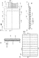
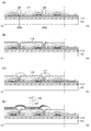
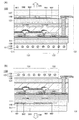
図1(A)は、表示装置100の上面図であり、図1(B)は、図1(A)中でA1−A2の一点鎖線で示す部位の断面図である。また、図1(C)は、図1(A)中でB1−B2の一点鎖線で示す部位の断面図である。また、図1(D)は、表示装置100の構成要素の一つである基板137の上面図である。
FIG. 1A is a top view of the
図1(A)に示す表示装置100は、基板111、基板121、基板137、および基板147を有する。また、表示装置100は、表示領域131、駆動回路132、駆動回路133、および外部電極124を有する。
A
図1(B)(C)に示すように、基板111と基板121とは互いに重なり、基板137と基板147とは、基板111と基板121とを介して、互いに重なっている。
As shown in FIGS. 1B and 1C, the
図1(D)に示す基板137は、絶縁体102と複数のガラス繊維103を含んでいる。複数のガラス繊維103のそれぞれは、Y方向に沿って延在している。このような基板137を表示装置100に取り付けることにより、表示装置100のY方向への屈曲に対する剛性を高めることができる。つまり、表示装置100のY方向への可撓性を低くすることができる。一方で、ガラス繊維103はY方向に沿って延在しているため、表示装置100のX方向への屈曲に対する剛性には影響を与えない。つまり、表示装置100のX方向への可撓性には影響を与えない。したがって、基板137を表示装置100に取り付けることにより、X方向へは容易に屈曲することができるが、Y方向へは屈曲しにくい表示装置100を実現することができる。
A
このように、図1(A)に示す表示装置100には、図1(D)に示す基板137が取り付けられているため、表示装置100のY方向への可撓性は、X方向への可撓性よりも十分に低くなっている。このため、表示装置100は、その取り扱い中に、X方向へは容易に屈曲するが、Y方向へは容易に屈曲しないので、X方向への曲げ軸とY方向への曲げ軸が交わる領域が生じにくく、結果として、表示装置100に大きな応力歪みが生じることを抑制することができる。
In this manner, since the
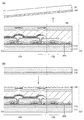
次に、図2(A)乃至図2(D)を用いて、表示装置100を屈曲させた状態について説明する。図2(A)は、図1(C)に相当し、図2(B)乃至図2(D)は、図2(A)に示す表示装置100をX方向へと屈曲させた状態を例示している。具体的には、図2(B)は、表示装置100をX方向へと折り曲げ、二つ折りにした状態を例示している。また、図2(C)は、表示装置100をX方向へと折り曲げ、三つ折りにした状態を例示している。また、図2(D)は、表示装置100をX方向へと折り曲げ、ロール状に巻いた状態を例示している。このように、表示装置100は、Y方向に沿って延在する複数のガラス繊維103を含む基板137が取り付けられているため、Y方向へは屈曲しにくいが、X方向へは容易に屈曲することができる。
Next, a state in which the
また、ガラス繊維103は復元性に優れているため、断線しにくく、表示装置100のY方向への可撓性を制御する材料として好ましい。
Further, since the
また、ガラス繊維103は導電性を有さないため、表示装置100が有する他の構成要素との間に不要な容量を生じることがなく、表示領域131の良好な表示を妨げない。
Further, since the
また、複数のガラス繊維103のそれぞれは糸状であり、その厚さあるいは幅に対してその長さが十分大きいものである。複数のガラス繊維103のそれぞれを、ビーズ状あるいは粉末状ではなく、糸状とすることで、表示装置100のY方向への可撓性を低くすることを制御性よく行うことができる。
Each of the plurality of
また、複数のガラス繊維103が延在する方向と、表示装置100を構成する配線が延在する方向をそろえることにより、配線が断線することを防ぐことができる。具体的には、例えば、複数のガラス繊維103がY方向に沿って延在し、表示装置100のY方向への可撓性が低くなっている場合に、表示装置100を構成する走査線あるいは信号線をY方向に沿って延在させることによって、走査線あるいは信号線を断線しにくくすることができる。
In addition, by aligning the direction in which the plurality of
このように、本発明の一態様によれば、可撓性を有し、屈曲可能であり、信頼性が高い表示装置、照明装置、もしくは電子機器を提供することができる。 As described above, according to one embodiment of the present invention, it is possible to provide a display device, a lighting device, or an electronic device that is flexible, bendable, and highly reliable.
または、本発明の一態様によれば、繰り返し屈曲可能な表示装置、照明装置、もしくは電子機器を提供することができる。 Alternatively, according to one embodiment of the present invention, a display device, a lighting device, or an electronic device that can be bent repeatedly can be provided.
または、本発明の一態様によれば、破損しにくい表示装置、照明装置、もしくは電子機器を提供することができる。 Alternatively, according to one embodiment of the present invention, a display device, a lighting device, or an electronic device which is not easily damaged can be provided.
または、本発明の一態様よれば、収納が容易であり、携帯性に優れた表示装置、照明装置、もしくは電子機器を提供することができる。 Alternatively, according to one embodiment of the present invention, a display device, a lighting device, or an electronic device that can be easily stored and has high portability can be provided.
なお、本実施の形態の表示装置100においては、Y方向に沿って延在する複数のガラス繊維103を含む基板137により、表示装置100のX方向への可撓性よりもY方向への可撓性を低くしているが、本発明の一態様は、これに限定されない。例えば、X方向に沿って延在する複数のガラス繊維103を含む基板137により、表示装置100のY方向への可撓性よりもX方向への可撓性を低くしてもよい。または、複数のガラス繊維103を斜め方向に沿って延在するようにしてもよい。その場合の例を、図34(A)に示す。
In the
また、本実施の形態の表示装置100においては、ガラス繊維103は、Y方向に沿って、基板の一端から他端まで途切れることなく延在しているが、本発明の一態様は、これに限定されない。例えば、ガラス繊維103は、Y方向に沿って、基板の一端よりも内側から基板の他端の内側まで延在していてもよい。また、ガラス繊維103は、途切れて形成されていてもよい。その場合の例を、図34(B)、図34(C)、および、図34(D)に示す。また、ガラス繊維103の厚さや密度を調整することによって、表示装置100の可撓性の程度を適宜調整してもよい。
In the
また、本実施の形態においては、表示装置100の可撓性の評価として、例えば、ヤング率を一つの指標とすることができる。例えば、表示装置100をX方向へと曲げた際のヤング率と、表示装置100をY方向へと曲げた際のヤング率をそれぞれ測定し、両者のヤング率を比較することにより、表示装置100のX方向への可撓性およびY方向への可撓性を評価することができる。X方向へと曲げた際のヤング率よりもY方向へと曲げた際のヤング率の方が高い場合には、表示装置100のY方向への可撓性は、X方向への可撓性よりも低いと結論づけることができる。なお、ヤング率の測定は、ISO527、JISK7161、JISK7162、JISK7127、ASTMD638、ASTMD882などを参考にして行うことができる。
In the present embodiment, as an evaluation of the flexibility of the
また、表示装置100の可撓性の評価として、例えば、曲率半径を一つの指標とすることができる。例えば、あらかじめ設定した力で表示装置100をX方向へと曲げ、その際の表示装置100の曲率半径を測定する。次に、同じ力で表示装置100をY方向へと曲げ、その際の表示装置100の曲率半径を測定する。そして、両者の曲率半径を比較することにより、表示装置100のX方向への可撓性およびY方向への可撓性を評価することができる。X方向へと曲げた際の曲率半径よりもY方向へと曲げた際の曲率半径の方が大きい場合には、表示装置100のY方向への可撓性は、X方向への可撓性よりも低いと結論づけることができる。例えば、本実施の形態の表示装置100においては、X方向へと曲げた際の曲率半径は20mm以下とすることができ、Y方向へと曲げた際の曲率半径は50mm以下とすることが困難である。つまり、この場合、本実施の形態の表示装置100においては、Y方向へと曲げた際の曲率半径の最小値は50mmである。より好ましくは、例えば、本実施の形態の表示装置100においては、X方向へと曲げた際の曲率半径は5mm以下とすることができ、Y方向へと曲げた際の曲率半径は100mm以下とすることが困難である。つまり、この場合、本実施の形態の表示装置100においては、Y方向へと曲げた際の曲率半径の最小値は100mmである。
Further, as an evaluation of the flexibility of the
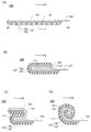
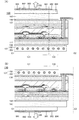
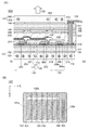
次に、図3を用いて、表示装置100の構成についてより詳細に説明する。図3(A)は、表示装置100の斜視図であり、図3(B)は、図3(A)中でC1−C2の一点鎖線で示す部位の断面図である。
Next, the configuration of the
<表示装置の構成例>
図3(A)(B)に示す本実施の形態の表示装置100は、表示領域131、駆動回路132、および駆動回路133を有する。また、表示装置100は、電極115、EL層117、電極118を含む発光素子125と、端子電極216を有する。発光素子125は、表示領域131中に複数形成されている。また、各発光素子125には、発光素子125の発光量を制御するトランジスタ232が接続されている。
<Configuration example of display device>
The
端子電極216は、開口122に形成された異方性導電接続層123を介して外部電極124と電気的に接続されている。また、端子電極216は、駆動回路132および駆動回路133に電気的に接続されている。なお、端子電極216は、表示領域131における構成要素と電気的に接続されていてもよい。
The
駆動回路132および駆動回路133は、複数のトランジスタ252により構成されている。駆動回路132および駆動回路133は、外部電極124から供給された信号を、表示領域131中のどの発光素子125に供給するかを決定する機能を有する。
The
トランジスタ232およびトランジスタ252は、ゲート電極206、ゲート絶縁層207、半導体層208、ソース電極209a、ドレイン電極209bを有する。また、ソース電極209a、およびドレイン電極209bと同一の膜を加工して得られた配線219が形成されている。また、トランジスタ232およびトランジスタ252上に絶縁層210が形成され、絶縁層210上に絶縁層211が形成されている。また、電極115が絶縁層211上に形成されている。電極115は、絶縁層210および絶縁層211に形成された開口を介してドレイン電極209bに電気的に接続されている。また、電極115上に隔壁114が形成され、電極115および隔壁114上に、EL層117および電極118が形成されている。
The
また、表示装置100は、接着層120を介して基板111と基板121が貼り合わされた構造を有する。また、基板111の一方の面に、接着層138を介して基板137が設けられている。また、基板121の一方の面に、接着層148を介して基板147が設けられている。なお、基板137は、絶縁体102と複数のガラス繊維103を含んでおり、複数のガラス繊維103のそれぞれはY方向に沿って延在している。このとき、ガラス繊維103と同様に、ソース電極209a、およびドレイン電極209bと同一の膜を加工して得られる配線219をY方向に沿って延在させることにより、配線219を断線しにくくすることができる。また、ガラス繊維103と同様に、ゲート電極206と同一の膜を加工して得られる図示しない配線をY方向に沿って延在させて断線しにくくすることもできる。また、ガラス繊維103は導電性を有さないため、例えば、ガラス繊維103とゲート電極206との間に不要な容量は形成されない。これにより、表示領域131の良好な表示が保たれる。
In addition, the
また、基板111の他方の面には、接着層112を介して絶縁層205が形成されている。なお、絶縁層205は下地層として機能し、基板111や接着層112などから、トランジスタ232や発光素子125への水分や不純物元素の拡散を防止、または低減することができる。
An insulating
また、基板121の他方の面には、接着層142を介して絶縁層145が形成され、絶縁層145を介して遮光層264が形成されている。また、基板121の他方の面には、絶縁層145を介して着色層266、オーバーコート層268が形成されている。なお、絶縁層145は下地層として機能し、基板121や接着層142などから、トランジスタ232や発光素子125への水分や不純物元素の拡散を防止、または低減することができる。
An insulating
基板111および基板121としては、有機樹脂材料などの可撓性を有する材料などを用いることができる。基板111および基板121として用いる材料の機械的強度が低すぎる場合、表示装置100の作製時に基板が変形しやすくなるため、歩留まりの低下など、生産性低下の一因となる。一方で、基板111および基板121として用いる材料の機械的強度が高すぎる場合は、表示装置が屈曲しにくくなってしまう。材料の機械的強度を表す指標の一つにヤング率がある。基板111および基板121に好適な材料のヤング率は、1GPa(1×10⁹Pa)以上100GPa(100×109Pa)以下、好ましくは2GPa以上50GPa以下、より好ましくは2GPa以上20GPa以下である。なお、ヤング率の測定は、ISO527、JISK7161、JISK7162、JISK7127、ASTMD638、ASTMD882などを参考にして行うことができる。
As the
基板111および基板121の厚さは、5μm以上100μm以下が好ましく、10μm以上50μm以下がより好ましい。また、基板111または基板121の一方、もしくは両方を、複数の層を有する積層基板としてもよい。また、基板111および基板121は、その目的に応じて、材料および厚さを適宜選択すればよい。
The thickness of the
また、基板121および基板111の熱膨張係数は、好ましくは30ppm/K以下、さらに好ましくは10ppm/K以下とする。また、基板121および基板111の表面に、予め窒化シリコンや酸化窒化シリコン等の窒素と珪素を含む膜や窒化アルミニウム等の窒素とアルミニウムを含む膜のような透水性の低い保護膜を成膜しておいてもよい。
The thermal expansion coefficients of the
本実施の形態の表示装置100は、光235が上面から射出する所謂トップエミッション構造(上面射出構造)であるため、基板121はEL層117からの発光に対して透光性を有する材料を用いる。なお、表示装置100を所謂ボトムエミッション構造(下面射出構造)の表示装置とする場合には、基板111にEL層117からの発光に対して透光性を有する材料を用いる。また、表示装置100を両面射出構造の表示装置とする場合には、基板111および基板121にEL層117からの発光に対して透光性を有する材料を用いる。
Since the
基板111および基板121に用いることができる、可撓性および可視光に対する透光性を有する材料の一例としては、ポリエチレンテレフタレート樹脂、ポリエチレンナフタレート樹脂、ポリアクリロニトリル樹脂、ポリイミド樹脂、ポリメチルメタクリレート樹脂、ポリカーボネート樹脂、ポリエーテルスルフォン樹脂、ポリアミド樹脂、シクロオレフィン樹脂、ポリスチレン樹脂、ポリアミドイミド樹脂、ポリ塩化ビニル樹脂、などがある。なお、光を透過させる必要がない場合には、非透光性の基板を用いてもよい。例えば、基板121または基板111として、アルミニウムなどを用いてもよい。
Examples of materials that can be used for the
基板137として、絶縁体102中に複数のガラス繊維103を含ませたものを用いることができる。
As the
絶縁体102の材料としては、例えば、シリコーンゴム、フッ素ゴムなどの粘弾性を有する高分子材料がある。例えば、複数のガラス繊維103を介して、シリコーンゴムからなる二枚のフィルムを貼り合わせることによって、基板137を形成してもよい。
Examples of the material of the
ガラス繊維103としては、Eガラス、Sガラス、Dガラス、Qガラス等を用いたガラス繊維が挙げられる。また、ガラス繊維103の厚さは、例えば、5μm以上100μm以下とすることができる。なお、ガラス繊維103の断面は、円形でも楕円形でも矩形でもよい。
Examples of the
また、例えば、X方向へと曲げた際の基板137のヤング率は、0.001GPa以上5GPa以下であり、Y方向へと曲げた際の基板137のヤング率は、X方向へと曲げた際の基板137のヤング率よりも高い。より好ましくは、X方向へと曲げた際の基板137のヤング率は0.01GPa以上1GPa以下であり、Y方向へと曲げた際の基板137のヤング率は50GPa以上である。
For example, the Young's modulus of the
また、ガラス繊維103は糸状であり、その厚さあるいは幅に対してその長さが十分大きいものである。ガラス繊維103を、ビーズ状あるいは粉末状ではなく、その厚さあるいは幅に対してその長さが十分大きな糸状とすることで、可撓性を低くしたい方向への表示装置100の可撓性の制御を適切に行うことができる。
Moreover, the
また、基板137として、複数のガラス繊維103に絶縁体102が含浸された構造物(所謂、プリプレグとも言う)を用いてもよい。プリプレグは、繊維体にマトリックス樹脂を有機溶剤で希釈したワニスを含浸させた後、乾燥して有機溶剤を揮発させてマトリックス樹脂を半硬化させたものである。この場合、絶縁体102としては、エポキシ樹脂、不飽和ポリエステル樹脂、ポリイミド樹脂、ビスマレイミドトリアジン樹脂またはシアネート樹脂等の熱硬化性樹脂を用いることができる。また、ポリフェニレンオキシド樹脂、ポリエーテルイミド樹脂またはフッ素樹脂等の熱可塑性樹脂を用いてもよい。
Alternatively, a structure in which a plurality of
なお、本実施の形態の表示装置100においては、ガラス繊維103を用いているが、本発明の一態様は、これに限定されない。例えば、引張弾性率またはヤング率の高い繊維である高強度繊維を用いることができ、例として、ポリビニルアルコール系繊維、ポリエステル系繊維、ポリアミド系繊維、ポリエチレン系繊維、アラミド系繊維、ポリパラフェニレンベンゾビスオキサゾール繊維、または炭素繊維が挙げられる。また、高強度繊維は、一種類の上記高強度繊維で形成されてもよいし、複数の上記高強度繊維で形成されてもよい。
Note that the
基板137の厚さは、基板111の2倍以上100倍以下が好ましく、5倍以上50倍以下がより好ましい。また、基板147の厚さは、基板121の2倍以上100倍以下が好ましく、5倍以上50倍以下がより好ましい。基板137を基板111よりも厚く、また、基板147を基板121よりも厚くすることで、応力緩和や緩衝材としての効果を良好なものとすることができる。
The thickness of the
また、基板137または基板147の一方、もしくは両方を、複数の層を有する積層基板としてもよい。また、基板137および基板147は、その目的に応じて、材料および厚さを適宜選択すればよい。
One or both of the
本実施の形態の表示装置100においては、光235が射出しない面側(非表示面側)に基板137が設けられ、光235が射出する面側(表示面側)に基板147が設けられている。これにより、基板137に含まれるガラス繊維103が光235と干渉することがないので、表示領域131の良好な表示を得ることができる。
In the
なお、ガラス繊維103を含む基板137を光235が射出する面側(表示面側)に設け、基板147を光235が射出しない面側(非表示面側)に設けてもよい。ガラス繊維103は透光性に優れた材料であるため、ガラス繊維103の厚さ、密度などを調整することにより、表示領域131の良好な表示を保ちつつ、ガラス繊維103を含む基板137を光235が射出する面側(表示面側)に設けることができる。
Note that the
また、基板137だけでなく基板147にもガラス繊維103を含ませてもよい。この場合、基板137に含まれるガラス繊維103と基板147に含まれるガラス繊維103の延在する方向をそろえることが好ましい。例えば、基板137に含まれる複数のガラス繊維103のそれぞれがY方向に沿って延在している場合には、基板147に含まれる複数のガラス繊維103のそれぞれもY方向に沿って延在していることが好ましい。これにより、表示装置100のY方向への可撓性を十分に低くすることができる。
Further, the
<変形例>
図4および図5に、表示装置100の変形例を示す。図1(C)は、図1(A)で示す表示装置100のB1−B2の一点鎖線で示す部位の断面図であるが、本発明の一態様は、これに限定されない。図4(A)乃至図4(F)は、図1(C)に示す表示装置100の断面構造の変形例を示している。また、図3(B)は、図3(A)で示す表示装置100のC1−C2の一点鎖線で示す部位の断面図であるが、本発明の一態様は、これに限定されない。図5は、図3(B)に示す表示装置100の断面構造の変形例を示している。
<Modification>
4 and 5 show a modification of the
図4(A)(C)(D)(E)(F)に示すように、外部電極124を基板111に接続することにより、外部電極124を簡単に接着できる。図5に示すように、異方性導電接続層123を介して、基板111上に形成された端子電極216と外部電極124とを接続している。また、図4(B)(C)(F)に示すように、外部電極124を基板147で覆うことにより、外部電極124と基板111との接続部を保護することができる。なお、図4(D)(E)(F)では、半導体チップ910が、COGなどにより、基板111上に設けられている場合を示している。図4(E)(F)に示すように、半導体チップ910を基板147で覆うことにより、半導体チップ910やその接続部を保護することができる。
As shown in FIGS. 4A, 4C, 4D, 4E, and 4F, by connecting the
<変形例>
図6に、表示装置100と異なる構成を有する表示装置200を示す。図6(A)は、表示装置200の上面図であり、図6(B)は、図6(A)中でA3−A4の一点鎖線で示す部位の断面図である。また、図6(C)は、図6(A)中でB3−B4の一点鎖線で示す部位の断面図である。
<Modification>
FIG. 6 shows a
表示装置200は、基板137および基板147の少なくとも一部が基板111および基板121の端部を超えて延伸し、該延伸部において、基板137および基板147が接続している点が、表示装置100と異なる。他の構成は表示装置100と同様に形成することができる。なお、該延伸部における基板137および基板147は、接着層などを介して間接的に接続してもよいし、直接接続してもよい。
In the
表示装置200のような構成とすることで、基板111および基板121端部からの不純物が侵入しにくくなるため、表示装置の信頼性をさらに高めることができる。
With the structure of the
<変形例>
図7に、表示装置200の変形例を示す。図6(C)は、図6(A)で示す表示装置200のB3−B4の一点鎖線で示す部位の断面図であるが、本発明の一態様は、これに限定されない。図7(A)乃至図7(H)は、図6(C)に示す表示装置200の断面構造の変形例を示している。
<Modification>
FIG. 7 shows a modification of the
図7(A)(C)(D)(E)(F)(G)(H)に示すように、外部電極124を基板111に接続することにより、外部電極124を簡単に接着できる。また、図7(B)(C)(D)(G)(H)に示すように、外部電極124を基板147で覆うことにより、外部電極124との接続部を保護することができる。また、図7(D)(H)に示すように、外部電極124を基板147と基板137とで覆うことにより、外部電極124と外部電極124と接続する基板との接続部をより保護することができる。なお、図7(E)(F)(G)(H)では、半導体チップ910が、COGなどにより、基板111上に設けられている場合を示している。また、図7(F)(G)(H)に示すように、半導体チップ910を基板147で覆うことにより、半導体チップ910やその接続部を保護することができる。
As shown in FIGS. 7A, 7C, 7D, 7E, 7G, and 7H, by connecting the
<画素回路構成例>
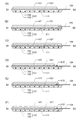
次に、図8を用いて、表示装置100のより具体的な構成例について説明する。図8(A)は、表示装置100の構成を説明するためのブロック図である。表示装置100は、表示領域131、駆動回路132、および駆動回路133を有する。駆動回路132は、例えば走査線駆動回路として機能する。また、駆動回路133は、例えば信号線駆動回路として機能する。
<Pixel circuit configuration example>
Next, a more specific configuration example of the
また、表示装置100は、各々が略平行に配設され、且つ、駆動回路132によって電位が制御されるm本の走査線135と、各々が略平行に配設され、且つ、駆動回路133によって電位が制御されるn本の信号線136と、を有する。このとき、走査線135あるいは信号線136が延在する方向とガラス繊維103が延在する方向をそろえることによって、表示装置100の取り扱い時に、走査線135あるいは信号線136が断線してしまうことを防ぐことができる。さらに、表示領域131はマトリクス状に配設された複数の画素134を有する。また、駆動回路132および駆動回路133をまとめて駆動回路部という場合がある。
Further, the
各走査線135は、表示領域131においてm行n列に配設された画素134のうち、いずれかの行に配設されたn個の画素134と電気的に接続される。また、各信号線136は、m行n列に配設された画素134のうち、いずれかの列に配設されたm個の画素134に電気的に接続される。m、nは、ともに1以上の整数である。
Each
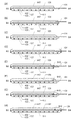
図8(B)および図8(C)は、図8(A)に示す表示装置の画素134に用いることができる回路構成を示している。
8B and 8C illustrate circuit structures that can be used for the
〔発光表示装置用画素回路の一例〕
また、図8(B)に示す画素134は、トランジスタ431と、容量素子233と、トランジスタ232と、発光素子125と、を有する。
[Example of pixel circuit for light-emitting display device]
A
トランジスタ431のソース電極およびドレイン電極の一方は、データ信号が与えられる配線(以下、信号線DL_nという)に電気的に接続される。さらに、トランジスタ431のゲート電極は、ゲート信号が与えられる配線(以下、走査線GL_mという)に電気的に接続される。
One of a source electrode and a drain electrode of the
トランジスタ431は、オン状態またはオフ状態になることにより、データ信号のノード435への書き込みを制御する機能を有する。
The
容量素子233の一対の電極の一方は、ノード435に電気的に接続され、他方は、ノード437に電気的に接続される。また、トランジスタ431のソース電極およびドレイン電極の他方は、ノード435に電気的に接続される。
One of the pair of electrodes of the
容量素子233は、ノード435に書き込まれたデータを保持する保持容量としての機能を有する。
The
トランジスタ232のソース電極およびドレイン電極の一方は、電位供給線VL_aに電気的に接続され、他方はノード437に電気的に接続される。さらに、トランジスタ232のゲート電極は、ノード435に電気的に接続される。
One of a source electrode and a drain electrode of the
発光素子125のアノードおよびカソードの一方は、電位供給線VL_bに電気的に接続され、他方は、ノード437に電気的に接続される。
One of an anode and a cathode of the light-emitting
発光素子125としては、例えば有機エレクトロルミネセンス素子(有機EL素子ともいう)などを用いることができる。ただし、発光素子125としては、これに限定されず、無機材料からなる無機EL素子を用いても良い。
As the light-emitting
なお、電位供給線VL_aおよび電位供給線VL_bの一方には、高電源電位VDDが与えられ、他方には、低電源電位VSSが与えられる。 Note that one of the potential supply line VL_a and the potential supply line VL_b is supplied with the high power supply potential VDD, and the other is supplied with the low power supply potential VSS.
図8(B)の画素134を有する表示装置では、駆動回路132により各行の画素134を順次選択し、トランジスタ431をオン状態にしてデータ信号をノード435に書き込む。
In the display device including the
ノード435にデータ信号が書き込まれた画素134は、トランジスタ431がオフ状態になることで保持状態になる。さらに、ノード435に書き込まれたデータの電位に応じてトランジスタ232のソース電極とドレイン電極の間に流れる電流量が制御され、発光素子125は、流れる電流量に応じた輝度で発光する。これを行毎に順次行うことにより、画像を表示できる。
The
〔液晶表示装置用画素回路の一例〕
図8(C)に示す画素134は、液晶素子432と、トランジスタ431と、容量素子233と、を有する。
[Example of pixel circuit for liquid crystal display device]
A
液晶素子432の一対の電極の一方の電位は、画素134の仕様に応じて適宜設定される。液晶素子432は、ノード436に書き込まれるデータにより配向状態が設定される。なお、複数の画素134のそれぞれが有する液晶素子432の一対の電極の一方に、共通の電位(コモン電位)を与えてもよい。また、各行の画素134毎の液晶素子432の一対の電極の一方に異なる電位を与えてもよい。
One potential of the pair of electrodes of the
例えば、液晶素子432を備える表示装置の駆動方法としては、TNモード、STNモード、VAモード、ASM(Axially Symmetric Aligned Micro−cell)モード、OCB(Optically Compensated Birefringence)モード、FLC(Ferroelectric Liquid Crystal)モード、AFLC(AntiFerroelectric Liquid Crystal)モード、MVAモード、PVA(Patterned Vertical Alignment)モード、IPSモード、FFSモード、またはTBA(Transverse Bend Alignment)モードなどを用いてもよい。また、表示装置の駆動方法としては、上述した駆動方法の他、ECB(Electrically Controlled Birefringence)モード、PDLC(Polymer Dispersed Liquid Crystal)モード、PNLC(Polymer Network Liquid Crystal)モード、ゲストホストモードなどがある。ただし、これに限定されず、液晶素子およびその駆動方式として様々なものを用いることができる。液晶素子を用いた表示装置の一例としては、液晶ディスプレイ(透過型液晶ディスプレイ、半透過型液晶ディスプレイ、反射型液晶ディスプレイ、直視型液晶ディスプレイ、投射型液晶ディスプレイ)などがある。なお、半透過型液晶ディスプレイや反射型液晶ディスプレイを実現する場合には、画素電極の一部、または、全部が、反射電極としての機能を有するようにすればよい。例えば、画素電極の一部、または、全部が、アルミニウム、銀、などを有するようにすればよい。さらに、その場合、反射電極の下に、SRAMなどの記憶回路を設けることも可能である。これにより、さらに、消費電力を低減することができる。
For example, as a driving method of a display device including the
また、ブルー相(Blue Phase)を示す液晶とカイラル剤とを含む液晶組成物により液晶素子432を構成してもよい。ブルー相を示す液晶は、応答速度が1msec以下と短く、光学的等方性であるため、配向処理が不要であり、視野角依存性が小さい。
Alternatively, the
なお、表示素子として、発光素子125および液晶素子432以外の表示素子を適用することも可能である。例えば、表示素子として、電気泳動素子、電子インク、エレクトロウェッティング素子、MEMS(マイクロ・エレクトロ・メカニカル・システム)、デジタルマイクロミラーデバイス(DMD)、DMS(デジタル・マイクロ・シャッター)、MIRASOL(登録商標)、IMOD(インターフェアレンス・モジュレーション)素子、シャッター方式のMEMS表示素子、光干渉方式のMEMS表示素子、などを用いることも可能である。
Note that as the display element, a display element other than the light-emitting
m行n列目の画素134において、トランジスタ431のソース電極およびドレイン電極の一方は、信号線DL_nに電気的に接続され、他方はノード436に電気的に接続される。トランジスタ431のゲート電極は、走査線GL_mに電気的に接続される。トランジスタ431は、オン状態またはオフ状態になることにより、ノード436へのデータ信号の書き込みを制御する機能を有する。
In the
容量素子233の一対の電極の一方は、特定の電位が供給される配線(以下、容量線CL)に電気的に接続され、他方は、ノード436に電気的に接続される。また、液晶素子432の一対の電極の他方はノード436に電気的に接続される。なお、容量線CLの電位の値は、画素134の仕様に応じて適宜設定される。容量素子233は、ノード436に書き込まれたデータを保持する保持容量としての機能を有する。
One of the pair of electrodes of the
例えば、図8(C)の画素134を有する表示装置では、駆動回路132により各行の画素134を順次選択し、トランジスタ431をオン状態にしてノード436にデータ信号を書き込む。
For example, in the display device including the
ノード436にデータ信号が書き込まれた画素134は、トランジスタ431がオフ状態になることで保持状態になる。これを行毎に順次行うことにより、画像を表示できる。
The
例えば、本明細書等において、画素に能動素子を有するアクティブマトリクス方式、または、画素に能動素子を有しないパッシブマトリクス方式を用いることができる。 For example, in this specification and the like, an active matrix method in which an active element is included in a pixel or a passive matrix method in which an active element is not included in a pixel can be used.
アクティブマトリクス方式では、能動素子(アクティブ素子、非線形素子)として、トランジスタだけでなく、さまざまな能動素子(アクティブ素子、非線形素子)を用いることができる。例えば、MIM(Metal Insulator Metal)、またはTFD(Thin Film Diode)などを用いることも可能である。これらの素子は、製造工程が少ないため、これらの素子を用いることで、製造コストの低減、又は歩留まりの向上を図ることができる。または、これらの素子は、素子のサイズが小さいため、開口率を向上させることができ、低消費電力化や高輝度化をはかることができる。 In the active matrix system, not only transistors but also various active elements (active elements, nonlinear elements) can be used as active elements (active elements, nonlinear elements). For example, MIM (Metal Insulator Metal) or TFD (Thin Film Diode) can be used. Since these elements have few manufacturing steps, the use of these elements can reduce the manufacturing cost or improve the yield. Alternatively, since these elements have small size, the aperture ratio can be improved, and power consumption and luminance can be increased.
アクティブマトリクス方式以外のものとして、能動素子(アクティブ素子、非線形素子)を用いないパッシブマトリクス型を用いることも可能である。能動素子(アクティブ素子、非線形素子)を用いないため、製造工程が少ないため、製造コストの低減、または歩留まりの向上を図ることができる。または、能動素子(アクティブ素子、非線形素子)を用いないため、開口率を向上させることができ、低消費電力化、又は高輝度化などを図ることができる。 As a method other than the active matrix method, a passive matrix type that does not use an active element (an active element or a non-linear element) can be used. Since no active element (active element or non-linear element) is used, the number of manufacturing steps is small, so that manufacturing costs can be reduced or yield can be improved. Alternatively, since an active element (an active element or a non-linear element) is not used, an aperture ratio can be improved, power consumption can be reduced, or luminance can be increased.
なお、ここでは、表示装置を用いて、様々な表示を行う場合の例を示したが、本発明の一態様は、これに限定されない。例えば、情報を表示しないようにしてもよい。一例としては、表示装置のかわりに、照明装置として用いてもよい。照明装置に適用することにより、デザイン性に優れたインテリアとして、活用することができる。または、様々な方向を照らすことができる照明として活用することができる。または、表示装置のかわりに、バックライトやフロントライトなどの光源として用いてもよい。つまり、表示パネルのための照明装置として活用してもよい。 Note that here, an example in the case where various displays are performed using a display device is described; however, one embodiment of the present invention is not limited thereto. For example, information may not be displayed. As an example, it may be used as a lighting device instead of a display device. By applying it to a lighting device, it can be used as an interior with excellent design. Or it can utilize as illumination which can illuminate various directions. Alternatively, a light source such as a backlight or a front light may be used instead of the display device. That is, you may utilize as an illuminating device for a display panel.
本実施の形態は、他の実施の形態に記載した構成と適宜組み合わせて実施することが可能である。 This embodiment can be implemented in appropriate combination with the structures described in the other embodiments.
(実施の形態2)
本実施の形態では、表示装置100の作製方法の一例について、図9乃至図16を用いて説明する。なお、図9乃至図15は、図3(A)中のC1−C2の一点鎖線で示す部位の断面に相当する。
(Embodiment 2)
In this embodiment, an example of a method for manufacturing the
<表示装置の作製方法例>
〔剥離層の形成〕
まず、素子形成基板101上に剥離層113を形成する(図9(A)参照。)。なお、素子形成基板101としては、ガラス基板、石英基板、サファイア基板、セラミック基板、金属基板などを用いることができる。また、本実施の形態の処理温度に耐えうる耐熱性を有するプラスチック基板を用いてもよい。
<Example of manufacturing method of display device>
(Formation of release layer)
First, the
また、ガラス基板には、例えば、アルミノシリケートガラス、アルミノホウケイ酸ガラス、バリウムホウケイ酸ガラスなどのガラス材料が用いられている。なお、酸化バリウム(BaO)を多く含ませることで、より実用的な耐熱ガラスが得られる。他にも、結晶化ガラスなどを用いることができる。 For the glass substrate, for example, a glass material such as aluminosilicate glass, aluminoborosilicate glass, or barium borosilicate glass is used. A more practical heat-resistant glass can be obtained by containing a large amount of barium oxide (BaO). In addition, crystallized glass or the like can be used.
剥離層113は、タングステン、モリブデン、チタン、タンタル、ニオブ、ニッケル、コバルト、ジルコニウム、ルテニウム、ロジウム、パラジウム、オスミウム、イリジウム、シリコンから選択された元素、または前記元素を含む合金材料、または前記元素を含む化合物材料を用いて形成することができる。また、これらの材料を単層又は積層して形成することができる。なお、剥離層113の結晶構造は、非晶質、微結晶、多結晶のいずれの場合でもよい。また、剥離層113を、酸化アルミニウム、酸化ガリウム、酸化亜鉛、二酸化チタン、酸化インジウム、インジウム錫酸化物、インジウム亜鉛酸化物、またはInGaZnO(IGZO)等の金属酸化物を用いて形成することもできる。
The
剥離層113は、スパッタリング法やCVD法、塗布法、印刷法等により形成できる。なお、塗布法はスピンコーティング法、液滴吐出法、ディスペンス法を含む。
The
剥離層113を単層で形成する場合、タングステン、モリブデン、またはタングステンとモリブデンを含む合金材料を用いることが好ましい。または、剥離層113を単層で形成する場合、タングステンの酸化物若しくは酸化窒化物、モリブデンの酸化物若しくは酸化窒化物、またはタングステンとモリブデンを含む合金の酸化物若しくは酸化窒化物を用いることが好ましい。
In the case where the
また、剥離層113として、例えば、タングステンを含む層とタングステンの酸化物を含む層の積層構造を形成する場合、タングステンを含む層に接して酸化物絶縁層を形成することで、タングステンを含む層と酸化物絶縁層との界面に、酸化タングステンが形成されることを活用してもよい。また、タングステンを含む層の表面を、熱酸化処理、酸素プラズマ処理、オゾン水等の酸化力の強い溶液での処理等を行ってタングステンの酸化物を含む層を形成してもよい。
For example, in the case where a stacked structure of a layer containing tungsten and a layer containing tungsten oxide is formed as the
本実施の形態では、素子形成基板101としてガラス基板を用いる。また、剥離層113として素子形成基板101上にスパッタリング法によりタングステンを形成する。
In this embodiment mode, a glass substrate is used as the
〔絶縁層の形成〕
次に、剥離層113上に下地層として絶縁層205を形成する(図9(A)参照。)。絶縁層205は、酸化シリコン、窒化シリコン、酸化窒化シリコン、窒化酸化シリコン、酸化アルミニウム、酸化窒化アルミニウム、または窒化酸化アルミニウム等を、単層または多層で形成するのが好ましい。例えば、絶縁層205を、酸化シリコンと窒化シリコンを積層した二層構造としてもよいし、上記材料を組み合わせた五層構造としてもよい。絶縁層205は、スパッタリング法やCVD法、熱酸化法、塗布法、印刷法等を用いて形成することが可能である。
(Formation of insulating layer)
Next, an insulating
絶縁層205の厚さは、30nm以上1μm以下、好ましくは50nm以上800nm以下とすればよい。
The thickness of the insulating
絶縁層205は、素子形成基板101や剥離層113などからの不純物元素の拡散を防止、または低減することができる。また、素子形成基板101を基板111に換えた後も、基板111や接着層112などから発光素子125への不純物元素の拡散を防止、または低減することができる。本実施の形態では、絶縁層205としてプラズマCVD法により厚さ200nmの酸化窒化シリコンと厚さ50nmの窒化酸化シリコンの積層膜を用いる。
The insulating
〔ゲート電極の形成〕
次に、絶縁層205上にゲート電極206を形成する(図9(A)参照。)。ゲート電極206は、アルミニウム、クロム、銅、タンタル、チタン、モリブデン、タングステンから選ばれた金属元素、または上述した金属元素を成分とする合金か、上述した金属元素を組み合わせた合金等を用いて形成することができる。また、マンガン、ジルコニウムのいずれか一または複数から選択された金属元素を用いてもよい。また、ゲート電極206は、単層構造でも、二層以上の積層構造としてもよい。例えば、シリコンを含むアルミニウム膜の単層構造、チタン膜上にアルミニウム膜を積層する二層構造、窒化チタン膜上にチタン膜を積層する二層構造、窒化チタン膜上にタングステン膜を積層する二層構造、窒化タンタル膜または窒化タングステン膜上にタングステン膜を積層する二層構造、チタン膜上に銅膜を積層する二層構造、チタン膜と、そのチタン膜上にアルミニウム膜を積層し、さらにその上にチタン膜を形成する三層構造等がある。また、アルミニウム、チタン、タンタル、タングステン、モリブデン、クロム、ネオジム、スカンジウムから選ばれた一または複数を組み合わせた合金膜、もしくは窒化膜を用いてもよい。
[Formation of gate electrode]
Next, the
また、ゲート電極206は、インジウム錫酸化物、酸化タングステンを含むインジウム酸化物、酸化タングステンを含むインジウム亜鉛酸化物、酸化チタンを含むインジウム酸化物、酸化チタンを含むインジウム錫酸化物、インジウム亜鉛酸化物、酸化シリコンを添加したインジウム錫酸化物等の透光性を有する導電性材料を適用することもできる。また、上記透光性を有する導電性材料と、上記金属元素の積層構造とすることもできる。
The
まず、絶縁層205上にスパッタリング法、CVD法、蒸着法等により、ゲート電極206となる導電膜を積層し、該導電膜上にフォトリソグラフィ工程によりレジストマスクを形成する。次に、レジストマスクを用いてゲート電極206となる導電膜の一部をエッチングして、ゲート電極206を形成する。この時、他の配線および電極も同時に形成することができる。
First, a conductive film to be the
導電膜のエッチングは、ドライエッチング法でもウエットエッチング法でもよく、両方を用いてもよい。なお、ドライエッチング法によりエッチングを行った場合、レジストマスクを除去する前にアッシング処理を行うと、剥離液を用いたレジストマスクの除去を容易とすることができる。 The conductive film may be etched by a dry etching method or a wet etching method, or both methods may be used. Note that in the case where etching is performed by a dry etching method, if the ashing treatment is performed before the resist mask is removed, the removal of the resist mask using a stripping solution can be facilitated.
なお、ゲート電極206は、上記形成方法の代わりに、電解メッキ法、印刷法、インクジェット法等で形成してもよい。
Note that the
ゲート電極206の厚さは、5nm以上500nm以下、より好ましくは10nm以上300nm以下、より好ましくは10nm以上200nm以下である。
The thickness of the
また、ゲート電極206を、遮光性を有する導電性材料を用いて形成することで、外部からの光が、ゲート電極206側から半導体層208に到達しにくくすることができる。その結果、光照射によるトランジスタの電気特性の変動を抑制することができる。
In addition, when the
〔ゲート絶縁層の形成〕
次に、ゲート絶縁層207を形成する(図9(A)参照。)。ゲート絶縁層207は、例えば酸化シリコン、酸化窒化シリコン、窒化酸化シリコン、窒化シリコン、酸化アルミニウム、酸化アルミニウムと酸化シリコンの混合物、酸化ハフニウム、酸化ガリウムまたはGa−Zn系金属酸化物などを用いればよく、積層または単層で設ける。
[Formation of gate insulating layer]
Next, the
また、ゲート絶縁層207として、ハフニウムシリケート(HfSiOx)、窒素が添加されたハフニウムシリケート(HfSixOyNz)、窒素が添加されたハフニウムアルミネート(HfAlxOyNz)、酸化ハフニウム、酸化イットリウムなどのhigh−k材料を用いることでトランジスタのゲートリークを低減できる。例えば、酸化窒化シリコンと酸化ハフニウムの積層としてもよい。
Further, as the
ゲート絶縁層207の厚さは、5nm以上400nm以下、より好ましくは10nm以上300nm以下、より好ましくは50nm以上250nm以下とするとよい。
The thickness of the
ゲート絶縁層207は、スパッタリング法、CVD法、蒸着法等で形成することができる。
The
ゲート絶縁層207として酸化シリコン膜、酸化窒化シリコン膜、または窒化酸化シリコン膜を形成する場合、原料ガスとしては、シリコンを含む堆積性気体および酸化性気体を用いることが好ましい。シリコンを含む堆積性気体の代表例としては、シラン、ジシラン、トリシラン、フッ化シラン等がある。酸化性気体としては、酸素、オゾン、一酸化二窒素、二酸化窒素等がある。
In the case where a silicon oxide film, a silicon oxynitride film, or a silicon nitride oxide film is formed as the
また、ゲート絶縁層207は、窒化物絶縁層と酸化物絶縁層をゲート電極206側から順に積層する積層構造としてもよい。ゲート電極206側に窒化物絶縁層を設けることで、ゲート電極206側から水素、窒素、アルカリ金属、またはアルカリ土類金属等が半導体層208に移動することを防ぐことができる。なお、一般に、窒素、アルカリ金属、またはアルカリ土類金属等は、半導体の不純物元素として機能する。また、水素は、酸化物半導体の不純物元素として機能する。よって、本明細書等における「不純物」には、水素、窒素、アルカリ金属、またはアルカリ土類金属等が含まれるものとする。
The
また、半導体層208として酸化物半導体を用いる場合は、半導体層208側に酸化物絶縁層を設けることで、ゲート絶縁層207と半導体層208の界面における欠陥準位密度を低減することが可能である。この結果、電気特性の劣化の少ないトランジスタを得ることができる。なお、半導体層208として酸化物半導体を用いる場合は、酸化物絶縁層として、化学量論的組成を満たす酸素よりも多くの酸素を含む酸化物絶縁層を用いて形成すると、ゲート絶縁層207と半導体層208の界面における欠陥準位密度をさらに低減することが可能であるため好ましい。
In the case where an oxide semiconductor is used for the
また、ゲート絶縁層207を、上記のように窒化物絶縁層と酸化物絶縁層の積層とする場合、酸化物絶縁層よりも窒化物絶縁層を厚くすることが好ましい。
In the case where the
窒化物絶縁層は酸化物絶縁層よりも比誘電率が大きいため、ゲート絶縁層207の膜厚を厚くしても、ゲート電極206に生じる電界を効率よく半導体層208に伝えることができる。また、ゲート絶縁層207を厚くすることで、ゲート絶縁層207の絶縁耐圧を高めることができる。よって、表示装置の信頼性を高めることができる。
Since the nitride insulating layer has a relative dielectric constant larger than that of the oxide insulating layer, the electric field generated in the
また、ゲート絶縁層207は、欠陥の少ない第1の窒化物絶縁層と、水素ブロッキング性の高い第2の窒化物絶縁層と、酸化物絶縁層とが、ゲート電極206側から順に積層される積層構造とすることができる。ゲート絶縁層207に、欠陥の少ない第1の窒化物絶縁層を用いることで、ゲート絶縁層207の絶縁耐圧を向上させることができる。特に、半導体層208として酸化物半導体を用いる場合は、ゲート絶縁層207に、水素ブロッキング性の高い第2の窒化物絶縁層を設けることで、ゲート電極206および第1の窒化物絶縁層に含まれる水素が半導体層208に移動することを防ぐことができる。
The
第1の窒化物絶縁層、第2の窒化物絶縁層の作製方法の一例を以下に示す。はじめに、シラン、窒素、およびアンモニアの混合ガスを原料ガスとして用いたプラズマCVD法により、欠陥の少ない窒化シリコン膜を第1の窒化物絶縁層として形成する。次に、原料ガスを、シランおよび窒素の混合ガスに切り替えて、水素濃度が少なく、且つ水素をブロッキングすることが可能な窒化シリコン膜を第2の窒化物絶縁層として成膜する。このような形成方法により、欠陥が少なく、且つ水素のブロッキング性を有する窒化物絶縁層が積層されたゲート絶縁層207を形成することができる。
An example of a method for manufacturing the first nitride insulating layer and the second nitride insulating layer is described below. First, a silicon nitride film with few defects is formed as a first nitride insulating layer by a plasma CVD method using a mixed gas of silane, nitrogen, and ammonia as a source gas. Next, the source gas is switched to a mixed gas of silane and nitrogen, and a silicon nitride film having a low hydrogen concentration and capable of blocking hydrogen is formed as the second nitride insulating layer. By such a formation method, the
また、ゲート絶縁層207は、不純物のブロッキング性が高い第3の窒化物絶縁層と、欠陥の少ない第1の窒化物絶縁層と、水素ブロッキング性の高い第2の窒化物絶縁層と、酸化物絶縁層とが、ゲート電極206側から順に積層される積層構造とすることができる。ゲート絶縁層207に、不純物のブロッキング性が高い第3の窒化物絶縁層を設けることで、ゲート電極206から水素、窒素、アルカリ金属、またはアルカリ土類金属等が半導体層208に移動することを防ぐことができる。
The
第1の窒化物絶縁層乃至第3の窒化物絶縁層の作製方法の一例を以下に示す。はじめに、シラン、窒素、およびアンモニアの混合ガスを原料ガスとして用いたプラズマCVD法により、不純物のブロッキング性が高い窒化シリコン膜を第3の窒化物絶縁層として形成する。次に、アンモニアの流量を増加させることで、欠陥の少ない窒化シリコン膜を第1の窒化物絶縁層として形成する。次に、原料ガスを、シランおよび窒素の混合ガスに切り替えて、水素濃度が少なく、且つ水素をブロッキングすることが可能な窒化シリコン膜を第2の窒化物絶縁層として形成する。このような形成方法により、欠陥が少なく、且つ不純物のブロッキング性を有する窒化物絶縁層が積層されたゲート絶縁層207を形成することができる。
An example of a method for manufacturing the first nitride insulating layer to the third nitride insulating layer is described below. First, a silicon nitride film having a high impurity blocking property is formed as a third nitride insulating layer by a plasma CVD method using a mixed gas of silane, nitrogen, and ammonia as a source gas. Next, by increasing the flow rate of ammonia, a silicon nitride film with few defects is formed as the first nitride insulating layer. Next, the source gas is switched to a mixed gas of silane and nitrogen, and a silicon nitride film having a low hydrogen concentration and capable of blocking hydrogen is formed as the second nitride insulating layer. With such a formation method, the
また、ゲート絶縁層207として酸化ガリウム膜を形成する場合、MOCVD(Metal Organic Chemical Vapor Deposition)法を用いて形成することができる。
In the case where a gallium oxide film is formed as the
なお、トランジスタのチャネルが形成される半導体層208と、酸化ハフニウムを含む絶縁層を、酸化物絶縁層を介して積層し、酸化ハフニウムを含む絶縁層に電子を注入することで、トランジスタのしきい値電圧を変化させることができる。
Note that a
〔半導体層の形成〕
半導体層208は、非晶質半導体、微結晶半導体、多結晶半導体等を用いて形成することができる。例えば、非晶質シリコン、多結晶シリコン、微結晶ゲルマニウム等を用いることができる。また、炭化シリコン、ガリウム砒素、酸化物半導体、窒化物半導体などの化合物半導体や、有機半導体等を用いることができる。酸化物半導体としては、非単結晶酸化物半導体、単結晶酸化物半導体などを用いることができる。非単結晶酸化物半導体としては、CAAC−OS(C Axis Aligned Crystalline Oxide Semiconductor)、多結晶酸化物半導体、微結晶酸化物半導体、非晶質酸化物半導体などを用いることができる。なお、CAAC−OSは、c軸配向した複数の結晶部を有する酸化物半導体の一つである。また、酸化物半導体は、代表的には、In−Ga酸化物、In−Zn酸化物、In−M−Zn酸化物(Mは、Ti、Ga、Y、Zr、La、Ce、Nd、SnまたはHf)がある。とくに、酸化物半導体としては、In−M−Zn酸化物(Mは、Ti、Ga、Y、Zr、La、Ce、Nd、SnまたはHf)を用いると好ましい。ただし、酸化物半導体は、インジウムを含む酸化物に限定されない。酸化物半導体は、例えば、Zn−Sn酸化物、Ga−Sn酸化物であっても構わない。
[Formation of semiconductor layer]
The
半導体層208の厚さは、3nm以上200nm以下、好ましくは3nm以上100nm以下、さらに好ましくは3nm以上50nm以下とする。本実施の形態では、半導体層208として、スパッタリング法により厚さ30nmの酸化物半導体膜を形成する。
The thickness of the
続いて、酸化物半導体膜上にレジストマスクを形成し、該レジストマスクを用いて酸化物半導体膜の一部を選択的にエッチングすることで、半導体層208を形成する。レジストマスクの形成は、フォトリソグラフィ法、印刷法、インクジェット法等を適宜用いて行うことができる。レジストマスクをインクジェット法で形成すると、フォトマスクを使用しないため、製造コストを低減できる。
Next, a resist mask is formed over the oxide semiconductor film, and the
酸化物半導体膜のエッチングは、ドライエッチング法でもウエットエッチング法でもよく、両方を用いてもよい。酸化物半導体膜のエッチング終了後、レジストマスクを除去する(図9(B)参照。)。 The oxide semiconductor film may be etched by a dry etching method or a wet etching method, or both methods may be used. After the oxide semiconductor film is etched, the resist mask is removed (see FIG. 9B).
〔電極の形成〕
次に、ソース電極209a、ドレイン電極209b、配線219、および端子電極216を形成する(図9(C)参照。)。まず、ゲート絶縁層207、半導体層208上に導電膜を形成する。
[Formation of electrodes]
Next, a
導電膜としては、アルミニウム、チタン、クロム、ニッケル、銅、イットリウム、ジルコニウム、モリブデン、銀、タンタル、またはタングステンなどの金属、またはこれを主成分とする合金で構成される単層構造または積層構造を用いることができる。例えば、シリコンを含むアルミニウム膜の単層構造、チタン膜上にアルミニウム膜を積層する二層構造、タングステン膜上にアルミニウム膜を積層する二層構造、銅−マグネシウム−アルミニウム合金膜上に銅膜を積層する二層構造、チタン膜上に銅膜を積層する二層構造、タングステン膜上に銅膜を積層する二層構造、チタン膜または窒化チタン膜と、そのチタン膜または窒化チタン膜上に重ねてアルミニウム膜または銅膜を積層し、さらにその上にチタン膜または窒化チタン膜を形成する三層構造、モリブデン膜または窒化モリブデン膜と、そのモリブデン膜または窒化モリブデン膜上に重ねてアルミニウム膜または銅膜を積層し、さらにその上にモリブデン膜または窒化モリブデン膜を形成する三層構造、タングステン膜上に銅膜を積層し、さらにその上にタングステン膜を形成する三層構造等がある。 As the conductive film, a single layer structure or a laminated structure made of a metal such as aluminum, titanium, chromium, nickel, copper, yttrium, zirconium, molybdenum, silver, tantalum, or tungsten, or an alloy containing the same as a main component is used. Can be used. For example, a single layer structure of an aluminum film containing silicon, a two layer structure in which an aluminum film is stacked on a titanium film, a two layer structure in which an aluminum film is stacked on a tungsten film, and a copper film on a copper-magnesium-aluminum alloy film Two-layer structure to stack, two-layer structure to stack a copper film on a titanium film, two-layer structure to stack a copper film on a tungsten film, a titanium film or a titanium nitride film, and an overlay on the titanium film or titanium nitride film A three-layer structure in which an aluminum film or a copper film is stacked and a titanium film or a titanium nitride film is further formed thereon, a molybdenum film or a molybdenum nitride film, and an aluminum film or a copper layer stacked on the molybdenum film or the molybdenum nitride film A three-layer structure in which a film is stacked and a molybdenum film or a molybdenum nitride film is formed thereon, and a copper film is stacked on the tungsten film And, there is a further three-layer structure in which a tungsten film is formed thereon.
なお、インジウム錫酸化物、亜鉛酸化物、酸化タングステンを含むインジウム酸化物、酸化タングステンを含むインジウム亜鉛酸化物、酸化チタンを含むインジウム酸化物、酸化チタンを含むインジウム錫酸化物、インジウム亜鉛酸化物、酸化ケイ素を添加したインジウム錫酸化物などの酸素を含む導電性材料、窒化チタン、窒化タンタルなどの窒素を含む導電性材料を用いてもよい。また、前述した金属元素を含む材料と、酸素を含む導電性材料を組み合わせた積層構造とすることもできる。また、前述した金属元素を含む材料と、窒素を含む導電性材料を組み合わせた積層構造とすることもできる。また、前述した金属元素を含む材料、酸素を含む導電性材料、および窒素を含む導電性材料を組み合わせた積層構造とすることもできる。 Indium tin oxide, zinc oxide, indium oxide including tungsten oxide, indium zinc oxide including tungsten oxide, indium oxide including titanium oxide, indium tin oxide including titanium oxide, indium zinc oxide, A conductive material containing oxygen such as indium tin oxide to which silicon oxide is added, or a conductive material containing nitrogen such as titanium nitride or tantalum nitride may be used. Alternatively, a stacked structure in which the above-described material containing a metal element and a conductive material containing oxygen are combined can be employed. Alternatively, a stacked structure in which the above-described material containing a metal element and a conductive material containing nitrogen are combined can be used. A stacked structure in which the above-described material containing a metal element, a conductive material containing oxygen, and a conductive material containing nitrogen can be combined.
また、導電膜の厚さは、5nm以上500nm以下、より好ましくは10nm以上300nm以下、より好ましくは10nm以上200nm以下である。本実施の形態では、導電膜として厚さ300nmのタングステン膜を形成する。 The thickness of the conductive film is 5 nm to 500 nm, more preferably 10 nm to 300 nm, and more preferably 10 nm to 200 nm. In this embodiment, a 300-nm-thick tungsten film is formed as the conductive film.
次に、レジストマスクを用いて、導電膜の一部を選択的にエッチングし、ソース電極209a、ドレイン電極209b、配線219、および端子電極216(これと同じ層で形成される他の電極または配線を含む)を形成する。レジストマスクの形成は、フォトリソグラフィ法、印刷法、インクジェット法等を適宜用いて行うことができる。レジストマスクをインクジェット法で形成するとフォトマスクを使用しないため、製造コストを低減できる。
Next, part of the conductive film is selectively etched using a resist mask, so that the
導電膜のエッチングは、ドライエッチング法でもウエットエッチング法でもよく、両方を用いてもよい。なお、エッチング工程により、露出した半導体層208の一部が除去される場合がある。導電膜のエッチング終了後、レジストマスクを除去する。表示領域131にはトランジスタ232が形成され、駆動回路133にはトランジスタ252が形成される(図9(C)参照。)。
The conductive film may be etched by a dry etching method or a wet etching method, or both methods may be used. Note that part of the exposed
〔絶縁層の形成〕
次に、ソース電極209a、ドレイン電極209b、配線219、および端子電極216上に、絶縁層210を形成する(図9(D)参照。)。絶縁層210は、絶縁層205と同様の材料および方法で形成することができる。
(Formation of insulating layer)
Next, the insulating
また、半導体層208に酸化物半導体を用いる場合は、少なくとも絶縁層210の半導体層208と接する領域に、酸素を含む絶縁層を用いることが好ましい。例えば、絶縁層210を複数層の積層とする場合、少なくとも半導体層208と接する層を酸化シリコンで形成すればよい。
In the case where an oxide semiconductor is used for the
〔開口の形成〕
次に、レジストマスクを用いて、絶縁層210の一部を選択的にエッチングし、開口128を形成する(図9(D)参照。)。この時、図示しない他の開口も同時に形成する。レジストマスクの形成は、フォトリソグラフィ法、印刷法、インクジェット法等を適宜用いて行うことができる。レジストマスクをインクジェット法で形成するとフォトマスクを使用しないため、製造コストを低減できる。
(Formation of opening)
Next, part of the insulating
絶縁層210のエッチングは、ドライエッチング法でもウエットエッチング法でもよく、両方を用いてもよい。
The insulating
開口128の形成により、ドレイン電極209b、端子電極216の一部が露出する。開口128の形成後、レジストマスクを除去する。
By forming the
〔平坦化膜の形成〕
次に、絶縁層210上に絶縁層211を形成する(図10(A)参照。)。絶縁層211は、絶縁層205と同様の材料および方法で形成することができる。
[Formation of planarization film]
Next, the insulating
また、発光素子125の被形成面の表面凹凸を低減するために、絶縁層211に平坦化処理を行ってもよい。平坦化処理として特に限定はないが、研磨処理(例えば、化学的機械研磨法(Chemical Mechanical Polishing:CMP))、やドライエッチング処理により行うことができる。
In addition, planarization treatment may be performed on the insulating
また、平坦化機能を有する絶縁材料を用いて絶縁層211を形成することで、研磨処理を省略することもできる。平坦化機能を有する絶縁材料として、例えば、ポリイミド樹脂、アクリル樹脂等の有機材料を用いることができる。また上記有機材料の他に、低誘電率材料(low−k材料)等を用いることができる。なお、これらの材料で形成される絶縁層を複数積層させることで、絶縁層211を形成してもよい。
In addition, by forming the insulating
また、開口128と重畳する領域の絶縁層211の一部を除去して、開口129を形成する。この時、図示しない他の開口部も同時に形成する。また、後に外部電極124が接続する領域の絶縁層211は除去する。なお、開口129等は、絶縁層211上にフォトリソグラフィ工程によるレジストマスクの形成を行い、絶縁層211のレジストマスクに覆われていない領域をエッチングすることで形成できる。開口129を形成することにより、ドレイン電極209bの表面を露出させる。
In addition, the
レジストマスクをインクジェット法で形成するとフォトマスクを使用しないため、製造コストを低減できる。また、絶縁層211に感光性を有する材料を用いることで、レジストマスクを用いることなく開口129を形成することができる。本実施の形態では、感光性のポリイミド樹脂を用いて絶縁層211および開口129を形成する。
When the resist mask is formed by an ink-jet method, a manufacturing cost can be reduced because a photomask is not used. In addition, by using a photosensitive material for the insulating
〔陽極の形成〕
次に、絶縁層211上に電極115を形成する(図10(B)参照。)。電極115は、後に形成されるEL層117が発する光を効率よく反射する導電性材料を用いて形成することが好ましい。なお、電極115は単層に限らず、複数層の積層構造としてもよい。例えば、電極115を陽極として用いる場合、EL層117と接する層を、インジウム錫酸化物などのEL層117よりも仕事関数が大きく透光性を有する層とし、その層に接して反射率の高い層(アルミニウム、アルミニウムを含む合金、または銀など)を設けてもよい。
[Formation of anode]
Next, the
なお、本実施の形態では、トップエミッション構造(上面射出構造)の表示装置について例示するが、ボトムエミッション構造(下面射出構造)、またはデュアルエミッション構造(両面射出構造)の表示装置とすることもできる。 Note that although a display device with a top emission structure (top emission structure) is illustrated in this embodiment mode, a display apparatus with a bottom emission structure (bottom emission structure) or a dual emission structure (double emission structure) may be used. .
表示装置100を、ボトムエミッション構造(下面射出構造)、またはデュアルエミッション構造(両面射出構造)の表示装置とする場合は、電極115に透光性を有する導電性材料を用いればよい。
In the case where the
電極115は、絶縁層211上に電極115となる導電膜を形成し、該導電膜上にレジストマスクを形成し、該導電膜のレジストマスクに覆われていない領域をエッチングすることで形成できる。該導電膜のエッチングは、ドライエッチング法、ウエットエッチング法、または双方を組み合わせたエッチング法を用いることができる。レジストマスクの形成は、フォトリソグラフィ法、印刷法、インクジェット法等を適宜用いて行うことができる。レジストマスクをインクジェット法で形成すると、フォトマスクを使用しないため、製造コストを低減できる。電極115の形成後、レジストマスクを除去する。
The
〔隔壁の形成〕
次に、隔壁114を形成する(図10(C)参照。)。隔壁114は、隣接する画素の発光素子125が意図せず電気的に短絡し、誤発光することを防ぐために設ける。また、後述するEL層117の形成にメタルマスクを用いる場合、メタルマスクが電極115に接触しないようにする機能も有する。隔壁114は、エポキシ樹脂、アクリル樹脂、イミド樹脂などの有機樹脂材料や、酸化シリコンなどの無機材料で形成することができる。隔壁114は、その側壁がテーパーまたは連続した曲率を持って形成される傾斜面となるように形成することが好ましい。隔壁114の側壁をこのような形状とすることで、後に形成されるEL層117や電極118の被覆性を良好なものとすることができる。
(Formation of partition walls)
Next, a
〔EL層の形成〕
EL層117は、少なくとも発光層を含んで形成されていればよく、発光層以外の機能層を含む積層構造であっても良い。発光層以外の機能層としては、正孔注入性の高い物質、正孔輸送性の高い物質、電子輸送性の高い物質、電子注入性の高い物質、バイポーラ性(電子および正孔の輸送性の高い物質)の物質等を含む層を用いることができる。具体的には、正孔注入層、正孔輸送層、電子輸送層、電子注入層等の機能層を適宜組み合わせて用いることができる。
[Formation of EL layer]
The
〔陰極の形成〕
本実施の形態では電極118を陰極として用いるため、電極118をEL層117に電子を注入できる仕事関数の小さい材料を用いて形成することが好ましい。また、仕事関数の小さい金属単体ではなく、仕事関数の小さいアルカリ金属、またはアルカリ土類金属を数nm形成した層を緩衝層として形成し、その上にアルミニウムなどの金属材料、インジウム錫酸化物等の導電性を有する酸化物材料、または半導体材料を用いて形成してもよい。また、緩衝層として、アルカリ土類金属の酸化物、ハロゲン化物、または、マグネシウム−銀等の合金を用いることもできる。
[Formation of cathode]
In this embodiment, since the
また、電極118を介して、EL層117が発する光を取り出す場合には、電極118は、可視光に対し透光性を有することが好ましい。電極115、EL層117、電極118により、発光素子125が形成される(図10(D)参照。)。
In the case where light emitted from the
〔対向素子形成基板の形成〕
遮光層264、着色層266、オーバーコート層268、絶縁層145、および剥離層143が形成された素子形成基板141を、接着層120を介して素子形成基板101上に形成する(図11(A)参照。)。なお、素子形成基板141は素子形成基板101と向かい合うように形成されるため、素子形成基板141を「対向素子形成基板」と呼ぶ場合がある。素子形成基板141(対向素子形成基板)の構成の詳細については、追って説明する。
[Formation of counter element forming substrate]
An
素子形成基板141は、素子形成基板101上に、接着層120により固定される。接着層120としては、光硬化型の接着剤、反応硬化型接着剤、熱硬化型接着剤、または嫌気型接着剤を用いることができる。例えば、エポキシ樹脂、アクリル樹脂、イミド樹脂等を用いることができる。トップエミッション構造(上面射出構造)の場合は接着層120に光の波長以下の大きさの乾燥剤(ゼオライト等)や、屈折率の大きいフィラー(酸化チタンや、ジルコニウム等)を混合すると、EL層117が発する光の取り出し効率が向上するため好適である。
The
〔素子形成基板の剥離〕
次に、剥離層113を介して絶縁層205と接する素子形成基板101を、絶縁層205から剥離する(図11(B)参照。)。剥離方法としては、機械的な力を加えること(人間の手や治具で引き剥がす処理や、ローラーを回転させながら分離する処理、超音波等)を用いて行えばよい。たとえば、剥離層113に鋭利な刃物またはレーザ光照射等で切り込みをいれ、その切り込みに水を注入する。または、その切り込みに霧状の水を吹き付ける。毛細管現象により水が剥離層113と絶縁層205の間にしみこむことにより、素子形成基板101を絶縁層205から容易に剥離することができる。
[Peeling of element forming substrate]
Next, the
〔基板の貼り合わせ〕
次に、接着層112を介して基板111を絶縁層205に貼り合わせる(図12(A)、図12(B)参照。)。接着層112は、接着層120と同様の材料を用いることができる。本実施の形態では、基板111として、厚さ20μm、ヤング率10GPaのアラミド(ポリアミド樹脂)を用いる。
[Lamination of substrates]
Next, the
〔素子形成基板の剥離〕
次に、剥離層143を介して絶縁層145と接する素子形成基板141を、絶縁層145から剥離する(図13(A)参照。)。素子形成基板141の剥離は、前述した素子形成基板101の剥離と同様の方法で行うことができる。
[Peeling of element forming substrate]
Next, the
〔基板の貼り合わせ〕
次に、接着層142を介して基板121を絶縁層145に貼り合わせる(図13(B)参照。)。接着層142は、接着層120と同様の材料を用いることができる。また、基板121は基板111と同様の材料を用いることができる。
[Lamination of substrates]
Next, the
〔開口の形成〕
次に、端子電極216および開口128と重畳する領域の、基板121、接着層142、絶縁層145、着色層266、オーバーコート層268、および接着層120を除去して、開口122を形成する(図14(A)参照。)。開口122を形成することにより、端子電極216の表面の一部が露出する。
(Formation of opening)
Next, the
〔外部電極の形成〕
次に、開口122に異方性導電接続層123を形成し、異方性導電接続層123上に、表示装置100に電力や信号を入力するための外部電極124を形成する(図14(B)参照)。端子電極216は、異方性導電接続層123を介して外部電極124と電気的に接続される。なお、外部電極124としては、例えばFPC(Flexible printed circuit)を用いることができる。
[Formation of external electrodes]
Next, the anisotropic
異方性導電接続層123は、異方性導電フィルム(ACF:Anisotropic Conductive Film)や、異方性導電ペースト(ACP:Anisotropic Conductive Paste)などを用いて形成することができる。
The anisotropic
異方性導電接続層123は、熱硬化性、又は熱硬化性および光硬化性の樹脂に導電性粒子を混ぜ合わせたペースト状又はシート状の材料を硬化させたものである。異方性導電接続層123は、光照射や熱圧着によって異方性の導電性を示す材料となる。異方性導電接続層123に用いられる導電性粒子としては、例えば球状の有機樹脂を金やニッケル、コバルト等の薄膜状の金属で被覆した粒子を用いることができる。
The anisotropic
〔基板の貼り合わせ〕
次に、基板137を、接着層138を介して基板111に貼り合わせる。また、基板147を、接着層148を介して基板121に貼り合わせる(図15参照。)。接着層138および接着層148は、接着層120と同様の材料を用いることができる。
[Lamination of substrates]
Next, the
基板137として、絶縁体102中に複数のガラス繊維103を含ませたものを用いる。複数のガラス繊維103のそれぞれは、Y方向に沿って延在している。また、複数のガラス繊維103のそれぞれは、互いに一定の間隔をあけて略平行に配置されている。
As the
本実施の形態では、絶縁体102として、可視光に対して透光性を有する厚さ200μm、ヤング率0.03GPaのシリコーンゴムを用いる。また、ガラス繊維103として、円形の断面を有し、直径が50μmのものを用いる。
In this embodiment, as the
また、本実施の形態では、基板147として、可視光に対して透光性を有する厚さ200μm、ヤング率0.03GPaのシリコーンゴムを用いる。
In this embodiment, a silicone rubber having a thickness of 200 μm and a Young's modulus of 0.03 GPa that transmits visible light is used as the
〔対向素子形成基板に形成される構造物〕
次に、素子形成基板141に形成される遮光層264などの構造物について、図16を用いて説明する。
[Structure formed on the counter element forming substrate]
Next, structures such as the
まず、素子形成基板141を準備する。素子形成基板141としては、素子形成基板101と同様の材料を用いることができる。次に、素子形成基板141上に剥離層143と絶縁層145を形成する(図16(A)参照。)。剥離層143は、剥離層113と同様の材料および方法で形成することができる。また、絶縁層145は、絶縁層205と同様の材料および方法で形成することができる。
First, the
次に、絶縁層145上に、遮光層264を形成する(図16(B)参照。)。その後、着色層266を形成する(図16(C)参照。)。
Next, a light-
遮光層264および着色層266は、様々な材料を用いて、印刷法、インクジェット法、フォトリソグラフィ法を用いて、それぞれ所望の位置に形成する。
The light-
次に、遮光層264および着色層266上にオーバーコート層268を形成する(図16(D)参照。)。
Next, an
オーバーコート層268としては、例えばアクリル樹脂、エポキシ樹脂、ポリイミド等の有機絶縁層を用いることができる。オーバーコート層268を形成することによって、例えば、着色層266中に含まれる不純物等を発光素子125側に拡散することを抑制することができる。ただし、オーバーコート層268は、必ずしも設ける必要はなく、オーバーコート層268を形成しない構造としてもよい。
As the
また、オーバーコート層268として透光性を有する導電膜を形成してもよい。オーバーコート層268として透光性を有する導電膜を設けることで、発光素子125から発せられた光235を透過し、かつ、イオン化した不純物の透過を防ぐことができる。
Alternatively, a light-transmitting conductive film may be formed as the
透光性を有する導電膜は、例えば、酸化インジウム、インジウム錫酸化物(ITO:Indium Tin Oxide)、インジウム亜鉛酸化物、酸化亜鉛、ガリウムを添加した酸化亜鉛などを用いて形成することができる。また、グラフェン等の他、透光性を有する程度に薄く形成された金属膜を用いてもよい。 The light-transmitting conductive film can be formed using, for example, indium oxide, indium tin oxide (ITO), indium zinc oxide, zinc oxide, zinc oxide to which gallium is added, or the like. In addition to graphene or the like, a metal film that is thin enough to have translucency may be used.
以上の工程で素子形成基板141に遮光層264などの構造物を形成することができる。
Through the above steps, a structure such as the
本実施の形態は、他の実施の形態に記載した構成と適宜組み合わせて実施することが可能である。 This embodiment can be implemented in appropriate combination with the structures described in the other embodiments.
(実施の形態3)
本実施の形態では、発光素子125に用いることができる発光素子の構成例について図17を用いて説明する。
(Embodiment 3)
In this embodiment, a structural example of a light-emitting element that can be used for the light-emitting
<発光素子の構成>
図17(A)に示す発光素子330は、一対の電極(電極318、電極322)間にEL層320が挟まれた構造を有する。なお、以下の本実施の形態の説明においては、例として、電極318を陽極として用い、電極322を陰極として用いるものとする。
<Configuration of light emitting element>
A light-emitting
また、EL層320は、少なくとも発光層を含んで形成されていればよく、発光層以外の機能層を含む積層構造であっても良い。発光層以外の機能層としては、正孔注入性の高い物質、正孔輸送性の高い物質、電子輸送性の高い物質、電子注入性の高い物質、バイポーラ性(電子および正孔の輸送性の高い物質)の物質等を含む層を用いることができる。具体的には、正孔注入層、正孔輸送層、電子輸送層、電子注入層等の機能層を適宜組み合わせて用いることができる。
Further, the
図17(A)に示す発光素子330は、電極318と電極322との間に生じた電位差により電流が流れ、EL層320において正孔と電子とが再結合し、発光するものである。つまりEL層320に発光領域が形成されるような構成となっている。
In the light-emitting
本発明において、発光素子330からの発光は、電極318、または電極322側から外部に取り出される。従って、電極318、または電極322のいずれか一方は透光性を有する物質で成る。
In the present invention, light emitted from the
なお、EL層320は図17(B)に示す発光素子331のように、電極318と電極322との間に複数積層されていても良い。n層(nは2以上の自然数)の積層構造を有する場合には、m番目(mは、1以上の自然数であり、m<nを満たす自然数)のEL層320と、(m+1)番目のEL層320との間には、それぞれ電荷発生層320aを設けることが好ましい。
Note that a plurality of EL layers 320 may be stacked between the
電荷発生層320aは、有機化合物と金属酸化物の複合材料、金属酸化物、有機化合物とアルカリ金属、アルカリ土類金属、またはこれらの化合物との複合材料の他、これらを適宜組み合わせて形成することができる。有機化合物と金属酸化物の複合材料としては、例えば、有機化合物と酸化バナジウムや酸化モリブデンや酸化タングステン等の金属酸化物を含む。有機化合物としては、芳香族アミン化合物、カルバゾール誘導体、芳香族炭化水素等の低分子化合物、または、それらの低分子化合物のオリゴマー、デンドリマー、ポリマー等など、種々の化合物を用いることができる。なお、有機化合物としては、正孔輸送性有機化合物として正孔移動度が10−6cm2/Vs以上であるものを適用することが好ましい。但し、電子よりも正孔の輸送性の高い物質であれば、これら以外のものを用いてもよい。なお、電荷発生層320aに用いるこれらの材料は、キャリア注入性、キャリア輸送性に優れているため、発光素子330の低電流駆動、および低電圧駆動を実現することができる。
The
なお、電荷発生層320aは、有機化合物と金属酸化物の複合材料と他の材料とを組み合わせて形成してもよい。例えば、有機化合物と金属酸化物の複合材料を含む層と、電子供与性物質の中から選ばれた一の化合物と電子輸送性の高い化合物とを含む層とを組み合わせて形成してもよい。また、有機化合物と金属酸化物の複合材料を含む層と、透明導電膜とを組み合わせて形成してもよい。
Note that the
このような構成を有する発光素子331は、エネルギーの移動や消光などの問題が起こりにくく、材料の選択の幅が広がることで高い発光効率と長い寿命とを併せ持つ発光素子とすることが容易である。また、一方の発光層で燐光発光、他方で蛍光発光を得ることも容易である。
The light-emitting
なお、電荷発生層320aとは、電極318と電極322に電圧を印加したときに、電荷発生層320aに接して形成される一方のEL層320に対して正孔を注入する機能を有し、他方のEL層320に電子を注入する機能を有する。
Note that the
図17(B)に示す発光素子331は、EL層320に用いる発光物質の種類を変えることにより様々な発光色を得ることができる。また、発光物質として発光色の異なる複数の発光物質を用いることにより、ブロードなスペクトルの発光や白色発光を得ることもできる。
The light-emitting
図17(B)に示す発光素子331を用いて、白色発光を得る場合、複数のEL層の組み合わせとしては、赤、青および緑色の光を含んで白色に発光する構成であればよく、例えば、青色の蛍光材料を発光物質として含む発光層と、緑色と赤色の燐光材料を発光物質として含む発光層を有する構成が挙げられる。また、赤色の発光を示す発光層と、緑色の発光を示す発光層と、青色の発光を示す発光層とを有する構成とすることもできる。または、補色の関係にある光を発する発光層を有する構成であっても白色発光が得られる。発光層が二層積層された積層型素子において、第1の発光層から得られる発光の発光色と第2の発光層から得られる発光の発光色を補色の関係にする場合、補色の関係としては、青色と黄色、あるいは青緑色と赤色などが挙げられる。
When white light emission is obtained using the light-emitting
なお、上述した積層型素子の構成において、積層される発光層の間に電荷発生層を配置することにより、電流密度を低く保ったまま、高輝度領域での発光が可能である。電流密度を低く保てるため、長寿命素子を実現することができる。また、電極材料の抵抗による電圧降下を小さくできるので、大面積での均一な発光が可能となる。 Note that in the structure of the stacked element described above, the charge generation layer is disposed between the stacked light emitting layers, whereby light emission in a high luminance region can be performed while keeping the current density low. Since the current density can be kept low, a long-life element can be realized. In addition, since the voltage drop due to the resistance of the electrode material can be reduced, uniform light emission over a large area is possible.
本実施の形態は、他の実施の形態に記載した構成と適宜組み合わせて実施することが可能である。 This embodiment can be implemented in appropriate combination with the structures described in the other embodiments.
(実施の形態4)
トップエミッション構造(上面射出構造)の表示装置100の構成を変形して、ボトムエミッション構造(下面射出構造)の表示装置150を作製することができる。
(Embodiment 4)
The
図18(A)(B)に、ボトムエミッション構造(下面射出構造)の表示装置150の断面構造の例を示す。なお、図18は、表示装置100の斜視図である図3(A)中でC1−C2の一点鎖線で示す部位と、同等の部位の断面図である。図18に示すボトムエミッション構造(下面射出構造)の表示装置150は、遮光層264、着色層266、およびオーバーコート層268の形成位置が、表示装置100と異なる。具体的には、表示装置150では、遮光層264、着色層266、およびオーバーコート層268が、基板111上に形成される。
18A and 18B show examples of a cross-sectional structure of a
また、表示装置150では、絶縁層145を基板121に直接形成して、接着層120を介して基板111と貼り合せることができる。すなわち、絶縁層145を素子形成基板141から転置する必要がないため、素子形成基板141、剥離層143、接着層142を不要とすることができる。よって、表示装置の生産性や歩留まりなどを向上することができる。
In the
なお、表示装置150の他の構成は、表示装置100と同様に形成することができる。
Note that other structures of the
また、ボトムエミッション構造の表示装置150は、電極115を、透光性を有する導電性材料を用いて形成され、電極118を、EL層117が発する光を効率よく反射する導電性材料を用いて形成される。
In the
表示装置150は、EL層117から発せられる光235を、着色層266を介して基板111側から射出することができる。
The
なお、図18(B)に示す表示装置150では、駆動回路133を構成するトランジスタとして、トランジスタ272を用いる例を示している。トランジスタ272は、トランジスタ252と同様に形成することができるが、絶縁層210上の、半導体層208と重畳する領域に電極263を有する点が異なる。電極263は、ゲート電極206と同様の材料および方法により形成することができる。
Note that the
電極263は、ゲート電極として機能させることができる。なお、ゲート電極206および電極263のどちらか一方を、単に「ゲート電極」という場合、他方を「バックゲート電極」という場合がある。また、ゲート電極206および電極263のどちらか一方を、「第1のゲート電極」といい、他方を「第2のゲート電極」という場合がある。
The
一般に、バックゲート電極は導電膜で形成され、ゲート電極とバックゲート電極で半導体層のチャネル形成領域を挟むように配置される。よって、バックゲート電極は、ゲート電極と同様に機能させることができる。バックゲート電極の電位は、ゲート電極と同電位としてもよく、GND電位や、任意の電位としてもよい。バックゲート電極の電位を変化させることで、トランジスタのしきい値電圧を変化させることができる。 In general, the back gate electrode is formed using a conductive film, and is arranged so that the channel formation region of the semiconductor layer is sandwiched between the gate electrode and the back gate electrode. Therefore, the back gate electrode can function in the same manner as the gate electrode. The potential of the back gate electrode may be the same as that of the gate electrode, or may be a GND potential or an arbitrary potential. By changing the potential of the back gate electrode, the threshold voltage of the transistor can be changed.
また、ゲート電極とバックゲート電極は導電膜で形成されるため、トランジスタの外部で生じる電界が、チャネルが形成される半導体層に作用しないようにする機能(特に静電気に対する静電遮蔽機能)も有する。 In addition, since the gate electrode and the back gate electrode are formed using a conductive film, an electric field generated outside the transistor does not act on a semiconductor layer in which a channel is formed (particularly, an electrostatic shielding function against static electricity). .
また、バックゲート電極側から光が入射する場合に、バックゲート電極を、遮光性を有する導電膜で形成することで、バックゲート電極側から半導体層に光が入射することを防ぐことができる。よって、半導体層の光劣化を防ぎ、トランジスタのしきい値電圧がシフトするなどの電気特性の劣化を防ぐことができる。 In addition, when light enters from the back gate electrode side, the back gate electrode is formed using a light-shielding conductive film, whereby light can be prevented from entering the semiconductor layer from the back gate electrode side. Therefore, light deterioration of the semiconductor layer can be prevented, and deterioration of electrical characteristics such as shift of the threshold voltage of the transistor can be prevented.
半導体層208を挟んでゲート電極206および電極263を設けることで、更にはゲート電極206および電極263を同電位とすることで、半導体層208においてキャリアの流れる領域が膜厚方向においてより大きくなるため、キャリアの移動量が増加する。この結果、トランジスタのオン電流が大きくなると共に、電界効果移動度が高くなる。
By providing the
また、ゲート電極206および電極263は、それぞれが外部からの電界を遮蔽する機能を有するため、ゲート電極206よりも下層、電極263よりも上層に存在する電荷が、半導体層208に影響することを抑制できる。この結果、ストレス試験(例えば、ゲートに負の電圧を印加する−GBT(Gate Bias−Temperature)ストレス試験)や、ゲートに正の電圧を印加する+GBTストレス試験の前後におけるしきい値電圧の変動が小さい。また、異なるドレイン電圧におけるオン電流の立ち上がり電圧の変動を抑制することができる。
In addition, since the
なお、BTストレス試験は加速試験の一種であり、長期間の使用によって起こるトランジスタの特性変化(即ち、経年変化)を、短時間で評価することができる。特に、BTストレス試験前後におけるトランジスタのしきい値電圧の変動量は、信頼性を調べるための重要な指標となる。BTストレス試験前後において、しきい値電圧の変動量が少ないほど、信頼性が高いトランジスタであるといえる。 Note that the BT stress test is a kind of accelerated test, and a change in characteristics (that is, a secular change) of a transistor caused by long-term use can be evaluated in a short time. In particular, the amount of change in the threshold voltage of the transistor before and after the BT stress test is an important index for examining reliability. Before and after the BT stress test, the smaller the variation amount of the threshold voltage, the higher the reliability of the transistor.
また、ゲート電極206および電極263を有し、且つゲート電極206および電極263を同電位とすることで、しきい値電圧の変動量が低減される。このため、複数のトランジスタにおける電気特性のばらつきも同時に低減される。
In addition, since the
なお、表示領域131中に形成されるトランジスタ232に、バックゲート電極を設けてもよい。
Note that a back gate electrode may be provided for the
本実施の形態は、他の実施の形態に記載した構成と適宜組み合わせて実施することが可能である。 This embodiment can be implemented in appropriate combination with the structures described in the other embodiments.
(実施の形態5)
トップエミッション構造(上面射出構造)の表示装置100の構成を変形して、遮光層264、着色層266、オーバーコート層268などを設けない表示装置160を作製することができる。
(Embodiment 5)
By changing the structure of the
図19(A)に、表示装置160の断面構造の例を示す。なお、図19は、表示装置100の斜視図である図3(A)中でC1−C2の一点鎖線で示す部位と、同等の部位の断面図である。表示装置160は、遮光層264、着色層266、およびオーバーコート層268を設けないかわりに、EL層117A、EL層117B、EL層117C(図示せず)などを用いることによって、カラー表示を行うことが出来る。EL層117A、EL層117Bなどは、それぞれ、赤、青、緑、などの異なる色で発光することができる。例えば、EL層117Aからは赤色の波長を有する光235Aが発せられ、EL層117Bからは青色の波長を有する光235Bが発せられ、EL層117Cからは緑色の波長を有する光235C(図示せず)が発せられる。
FIG. 19A illustrates an example of a cross-sectional structure of the
また、着色層266を用いないことによって、光235A、光235B、および光235Cが着色層266を透過する際に生じる輝度の低下を無くすことが出来る。また、光235A、光235B、および光235Cの波長に応じて、EL層117A、EL層117B、およびEL層117Cの厚さを調整することで、色純度を向上させることができる。
Further, by not using the
なお、表示装置160と同様に、ボトムエミッション構造(下面射出構造)の表示装置150の構成を変形して、遮光層264、着色層266、オーバーコート層268などを設けない表示装置170も作製することができる。図19(B)に、表示装置170の断面構造の例を示す。
Note that similarly to the
なお、図20(A)(B)に示すように、偏光板、位相差板、λ/4板などの光学フィルム911を追加で配置してもよい。光学フィルム911は、接着層148Aを用いて、基板111あるいは基板121に接着されている。このような配置とすることにより、画面表面での反射を低減することができる。
As shown in FIGS. 20A and 20B, an
なお、表示装置160および表示装置170の他の構成は、表示装置100と同様に形成することができる。
Note that other structures of the
本実施の形態は、他の実施の形態に記載した構成と適宜組み合わせて実施することが可能である。 This embodiment can be implemented in appropriate combination with the structures described in the other embodiments.
(実施の形態6)
図21(A)に示すように、表示装置100において、基板147の上に、タッチセンサを有する基板を設けてもよい。タッチセンサは、導電層991と導電層993などを用いて構成されている。また、それらの間には、絶縁層992が設けられている。
(Embodiment 6)
As shown in FIG. 21A, in the
なお、導電層991および導電層993は、インジウム錫酸化物やインジウム亜鉛酸化物などの透明導電膜を用いることが望ましい。ただし、抵抗を下げるため、導電層991および導電層993の一部、または、全部に、低抵抗な材料を持つ層を用いてもよい。例えば、アルミニウム、チタン、クロム、ニッケル、銅、イットリウム、ジルコニウム、モリブデン、銀、タンタル、またはタングステンなどの金属、またはこれを主成分とする合金を単層構造または積層構造を用いることができる。または、導電層991および導電層993として、金属ナノワイヤを用いてもよい。その場合の金属としては、銀などが好適である。これにより、抵抗値を下げることができるため、センサの感度を向上させることができる。
Note that the
絶縁層992は、酸化シリコン、窒化シリコン、酸化窒化シリコン、窒化酸化シリコン、酸化アルミニウム、酸化窒化アルミニウム、または窒化酸化アルミニウム等を、単層または多層で形成するのが好ましい。絶縁層992は、スパッタリング法やCVD法、熱酸化法、塗布法、印刷法等を用いて形成することができる。
The insulating
なお、タッチセンサは、基板994の上に設けられているが、本発明の一態様は、これに限定されない。基板994の下(基板121と基板994との間)に設けられていてもよい。
Note that although the touch sensor is provided over the
また、図21(B)に示すように、タッチセンサを有する基板を、表示装置150において、基板147の下側に設けてもよい。
In addition, as illustrated in FIG. 21B, a substrate having a touch sensor may be provided below the
また、図22(A)に示すように、タッチセンサを、基板121の上に、接着層148Aを介して配置してもよい。また、図22(B)に示すように、タッチセンサを、基板111の下に、接着層148Aを介して配置してもよい。
In addition, as illustrated in FIG. 22A, the touch sensor may be disposed over the
なお、基板994として、光学フィルムの機能を持たせてもよい。つまり、基板994は、偏光板や位相差板などの機能を有していてもよい。
Note that the
また、表示装置100において、タッチセンサを基板121に形成してもよい。図23(A)は、基板121にタッチセンサを形成し、タッチセンサおよび接着層148を介して基板147を形成する例を示している。
In the
また、表示装置150において、タッチセンサを基板111に形成してもよい。図23(B)は、基板111にタッチセンサを形成し、タッチセンサおよび接着層148を介して基板147を形成する例を示している。
In the
また、表示装置160において、タッチセンサを基板121に形成してもよい。図24(A)は、基板121にタッチセンサを形成し、タッチセンサおよび接着層148を介して基板147を形成する例を示している。
In the
また、表示装置170において、タッチセンサを基板111に形成してもよい。図24(B)は、基板111にタッチセンサを形成し、タッチセンサおよび接着層148を介して基板147を形成する例を示している。
Further, in the
なお、図24(A)に示す表示装置160および図24(B)に示す表示装置170において、光学フィルム911を配置してもよい。その場合の例を図25(A)(B)に示す。光学フィルム911は、接着層148Aを介して、基板111および基板121に接着されている。
Note that an
なお、タッチセンサとして、静電容量式のタッチセンサや、pn型又はpin型のフォトダイオードなどの受光素子を備えるタッチセンサを利用することができる。 As the touch sensor, a capacitive touch sensor or a touch sensor including a light receiving element such as a pn-type or pin-type photodiode can be used.
本実施の形態は、他の実施の形態に記載した構成と適宜組み合わせて実施することが可能である。 This embodiment can be implemented in appropriate combination with the structures described in the other embodiments.
(実施の形態7)
本実施の形態では、表示装置100において、基板111および基板121を省略する場合について図26を用いて説明する。図26は、表示装置100の斜視図である図3(A)中でC1−C2の一点鎖線で示す部位と、同等の部位の断面図である。
(Embodiment 7)
In this embodiment, the case where the
図26(A)に示す表示装置100は、図3(B)に示す表示装置100と基板111を省略している点で異なる。
A
図26(A)に示す表示装置100においては、基板137中に複数のガラス繊維103が含まれているので、基板137が高い機械的強度を有している。したがって、基板111を設けなくとも、表示装置100の作製時に基板が変形することを防ぐことができる。また、基板111を設けなくとも、表示装置100の取り扱い時における機械的強度を満足することができる。
In the
また、基板137中に含まれるガラス繊維103の厚さを厚くする、あるいは密度を高くすることにより、基板137により高い機械的強度を持たせることができる。これにより、基板111を設けなくとも、表示装置100の作製時に基板が変形することをより確実に防ぐことができる。また、基板111を設けなくとも、表示装置100の取り扱い時における機械的強度をより満足することができる。
Further, by increasing the thickness of the
図26(A)に示す表示装置100においては、基板111を省略することができるので、基板111を接着するための接着層112を省略することもできる。これにより、薄型化および軽量化を達成し、携帯性に優れた表示装置、照明装置、もしくは電子機器を提供することができる。
In the
また、表示装置100の下側を、癖のつきやすい基板111を用いず、基板137のみによって構成することができる。これにより、表示装置100を繰り返し屈曲させた場合であっても、表示装置100に癖がつきにくい。この場合の癖とは、例えば、表示装置100がX方向に勝手に曲がってしまうような癖や、表示装置100をX方向に繰り返し屈曲させた後に生じる残留歪み、しわなどが挙げられる。したがって、その取り扱い中に癖をほとんどつけずに繰り返し屈曲可能な表示装置、照明装置、もしくは電子機器を提供することができる。
In addition, the lower side of the
図26(B)に示す表示装置100は、基板111に加えて、基板121も省略している。図26(B)に示す表示装置100は、図5に示す表示装置100と、基板111および基板121を省略している点で異なる。表示装置100の作製時に基板が変形しない程度に、基板137中に複数のガラス繊維103を含ませ、基板137に高い機械的強度を持たせることにより、基板111に加えて、基板121も省略することが可能である。
In the
本実施の形態によれば、基板111および基板121を省略することができるので、基板111および基板121を接着するための接着層112および接着層142も省略することができる。これにより、さらなる薄型化および軽量化を達成し、携帯性に優れた表示装置、照明装置、もしくは電子機器を提供することができる。
According to this embodiment, since the
また、表示装置100を構成する基板として、癖のつきやすい基板111および基板121を用いず、基板147および基板137のみを用いることができる。これにより、表示装置100を繰り返し屈曲させた場合であっても、表示装置100に癖がつきにくい。この場合の癖とは、例えば、表示装置100がX方向に勝手に曲がってしまうような癖や、表示装置100をX方向に繰り返し屈曲させた後に生じる残留歪み、しわなどが挙げられる。したがって、その取り扱い中に癖をほとんどつけずに繰り返し屈曲可能な表示装置、照明装置、もしくは電子機器を提供することができる。
Further, only the
本実施の形態は、他の実施の形態に記載した構成と適宜組み合わせて実施することが可能である。 This embodiment can be implemented in appropriate combination with the structures described in the other embodiments.
(実施の形態8)
本実施の形態では、表示装置100において、光235が射出する面側(表示面側)に複数のガラス繊維103を配置する場合について図27を用いて説明する。具体的には、光235が射出する面側(表示面側)に設けられた基板147中に、複数のガラス繊維103を含ませる場合について説明する。図27(A)は、表示装置100の斜視図である図3(A)中でC1−C2の一点鎖線で示す部位と、同等の部位の断面図である。
(Embodiment 8)
In this embodiment, the case where a plurality of
図27(A)に示す表示装置100は、図3(B)に示す表示装置100と基板147中に複数のガラス繊維103を含ませている点で異なる。
A
図27(A)に示す表示装置100においては、基板147中に複数のガラス繊維103を含ませている。基板147は、基板137と同様の材料および方法で形成することができる。また、図27(B)で示すように、基板147中の複数のガラス繊維103はY方向に沿って延在している。
In the
基板147中に含まれる複数のガラス繊維103と、基板137中に含まれる複数のガラス繊維103の延在する方向をY方向でそろえることにより、表示装置100のY方向への可撓性をより十分に低くすることができる。これにより、表示装置100は、X方向へは容易に屈曲することができるが、Y方向へはより屈曲しにくくなり、X方向への曲げ軸とY方向への曲げ軸とが交わる領域が生じにくく、その取り扱い中に、ある特定の領域に大きな力が加わり、当該領域において配線間ショートのような動作不良が発生することをより確実に防止することができる。
By aligning the extending direction of the plurality of
また、基板147中に含まれるガラス繊維103の密度は、その領域によって適宜変更することができる。具体的には、基板147中に含まれるガラス繊維103の密度を、表示領域131では低くすることが好ましい。
Moreover, the density of the
図27(B)に本実施の形態における基板147を示す。なお、図27(B)において、表示領域131に対応する領域を領域131a、駆動回路132に対応する領域を領域132a、駆動回路133に対応する領域を領域133aとする。図27(B)に示すように、基板147中のガラス繊維103の密度を、領域131aでは低く、領域133aでは高くすることができる。これにより、基板147中に含まれるガラス繊維103と光235との干渉を最小限とすることができ、表示装置100の良好な表示を保つことができる。また、本実施の形態では、透光性に優れるガラス繊維103を用いているので、領域131aに配置されたガラス繊維103が光235に与える影響を小さくすることができる。
FIG. 27B illustrates a
本実施の形態の表示装置100は、良好な表示を保ちつつ、Y方向への可撓性がX方向への可撓性より十分に低くなっている。したがって、本実施の形態によれば、良好な表示を保ちつつ、その取り扱い中に破損することなく、繰り返し屈曲可能であり、信頼性が高い表示装置、照明装置、もしくは電子機器を提供することができる。
The
なお、複数のガラス繊維103を有する基板137を、光235が射出する面側(表示面側)に設ける場合にも、上記と同様にガラス繊維103の密度を調整することができる。
Note that in the case where the
本実施の形態は、他の実施の形態に記載した構成と適宜組み合わせて実施することが可能である。 This embodiment can be implemented in appropriate combination with the structures described in the other embodiments.
(実施の形態9)
複数のガラス繊維103に加えて、基板137中に複数の繊維104を含ませる場合について図28を用いて説明する。具体的には、基板137中に、ガラス繊維103と交差するように、ガラス繊維103よりも引張弾性率またはヤング率の低い繊維104を含ませる場合について説明する。図28(A)は、基板137の上面図である図1(D)と対応する。
(Embodiment 9)
A case where a plurality of
図28(A)に示す基板137は、Y方向に沿って延在する複数のガラス繊維103と、X方向に沿って延在する複数の繊維104を有する。この場合、繊維104は、ガラス繊維103よりもやわらかいもの、引張弾性率またはヤング率の低いものを用いることが好ましい。これより、Y方向への可撓性がX方向への可撓性よりも低い状態を保ちつつ、基板137の機械的強度を高めることができる。
A
図28(B)は、図28(A)中でA1−A2の一点鎖線で示す部位の断面図である。また、図28(C)は、図28(A)中でB1−B2の一点鎖線で示す部位の断面図である。図28(B)(C)で示すように、繊維104はガラス繊維103に編み込むように設けることができる。ただし、これに限定されず、繊維104を、ガラス繊維103の上あるいは下に設けて、積層構造としてもよい。また、例えば、ガラス繊維103を含んだ絶縁体102と、繊維104を含んだ絶縁体102の積層構造としてもよい。
FIG. 28B is a cross-sectional view taken along the dashed-dotted line A1-A2 in FIG. FIG. 28C is a cross-sectional view taken along the dashed-dotted line B1-B2 in FIG. As shown in FIGS. 28B and 28C, the
本実施の形態によれば、基板137の機械的強度を高めることができるので、実施の形態7で説明したように、表示装置100を構成する基板111および基板121を省略することができる。
According to this embodiment, since the mechanical strength of the
また、本実施の形態の基板137に表示装置、照明装置、もしくは電子機器の光の拡散板としての機能を持たせることもできる。
In addition, the
本実施の形態は、他の実施の形態に記載した構成と適宜組み合わせて実施することが可能である。 This embodiment can be implemented in appropriate combination with the structures described in the other embodiments.
(実施の形態10)
表示装置を構成する発光素子125やトランジスタ232が中立面に位置するように基板の構成を調整する手段について、図29を用いて説明する。なお、中立面とは、曲げなどの変形に対して引張応力や圧縮応力などの応力歪みが発生しない面(延び縮みしない面)を指す。
(Embodiment 10)
Means for adjusting the structure of the substrate so that the light-emitting
図29(A)に示す表示装置は、下側から、基板137、基板111、図示しない発光素子125やトランジスタ232など、基板121、基板147を有している。基板111および基板121は、同じ厚さで、同じ材料から形成されている。また、基板137および基板147は、同じ厚さで、同じ材料から形成されている。この場合、中立面は表示装置の厚さ方向における真ん中となり、具体的には、中立面は一点鎖線D1−D2で示す箇所に位置する。したがって、図29(A)に示す表示装置においては、発光素子125やトランジスタ232などは、中立面に位置している。
The display device illustrated in FIG. 29A includes a
ここで、図29(A)に示す表示装置を構成する基板137中に複数のガラス繊維103を設けた場合、基板137のヤング率は基板147のヤング率より高くなり、中立面は表示装置の厚さ方向における真ん中よりも基板137側に移動する可能性がある。具体的には、中立面は、一点鎖線D1−D2で示す箇所よりも基板137側に移動する可能性がある。この場合、機械的強度が高くない発光素子125やトランジスタ232などは、中立面に位置していないため、表示装置の屈曲時に、応力歪みにより壊れてしまうおそれがある。
Here, in the case where a plurality of
図29(B)に示す表示装置は、下側から、絶縁体102とガラス繊維103とを含む基板137、基板111、図示しない発光素子125やトランジスタ232など、基板121、基板147を有している。基板111および基板121は、同じ厚さで、同じ材料から形成されている。また、基板147の厚さは基板137よりも厚くなっている。ガラス繊維103を含む基板137のヤング率はガラス繊維を含まない基板147のヤング率より高いため、中立面は表示装置の厚さ方向における真ん中よりも基板137側に移動するものの、基板147の厚さを基板137よりも厚くしているため、結果として、発光素子125やトランジスタ232は中立面に位置することができる。
The display device illustrated in FIG. 29B includes, from below, a
具体的には、図29(B)に示す表示装置において、中立面は表示装置の厚さ方向における真ん中よりも基板137側である一点鎖線E1−E2で示す箇所に位置するが、基板147が基板137よりも厚いため、その中立面の位置は基板111と基板121との間に形成されている発光素子125やトランジスタ232の位置と一致している。したがって、表示装置の屈曲時に、発光素子125やトランジスタ232などが応力歪みにより壊れることを防止できる。
Specifically, in the display device illustrated in FIG. 29B, the neutral plane is located at a position indicated by a dashed-dotted line E1-E2 that is closer to the
本実施の形態によれば、基板137にガラス繊維103を含ませつつ、発光素子125やトランジスタ232などが中立面に位置するようにできるので、その取り扱い中に破損することなく、繰り返し屈曲可能であり、信頼性が高い表示装置、照明装置、もしくは電子機器を提供することができる。
According to this embodiment, since the
本実施の形態では、基板147の厚さを基板137の厚さよりも厚くする手段を説明したが、本発明の一態様は、これに限定されない。例えば、基板147に別の基板を接着した積層構造としてもよい。また、基板121の厚さを基板111の厚さよりも厚くしてもよい。
In this embodiment, the means for making the thickness of the
本実施の形態は、他の実施の形態に記載した構成と適宜組み合わせて実施することが可能である。 This embodiment can be implemented in appropriate combination with the structures described in the other embodiments.
(実施の形態11)
本実施の形態では、本発明の一態様の表示装置が適用された電子機器や照明装置の例について、図面を参照して説明する。
(Embodiment 11)
In this embodiment, examples of electronic devices and lighting devices to which the display device of one embodiment of the present invention is applied are described with reference to drawings.
フレキシブルな形状を備える表示装置を適用した電子機器として、例えば、テレビジョン装置(テレビ、又はテレビジョン受信機ともいう)、コンピュータ用などのモニタ、デジタルカメラ、デジタルビデオカメラ、デジタルフォトフレーム、携帯電話機(携帯電話、携帯電話装置ともいう)、携帯型ゲーム機、携帯情報端末、音響再生装置、パチンコ機などの大型ゲーム機などが挙げられる。 As an electronic apparatus to which a display device having a flexible shape is applied, for example, a television device (also referred to as a television or a television receiver), a monitor for a computer, a digital camera, a digital video camera, a digital photo frame, a mobile phone (Also referred to as a mobile phone or a mobile phone device), a portable game machine, a portable information terminal, a sound reproduction device, a large game machine such as a pachinko machine, and the like.
また、表示装置を、家屋やビルの内壁または外壁や、自動車の内装または外装の曲面に沿って組み込むことも可能である。 It is also possible to incorporate the display device along an inner wall or an outer wall of a house or a building, or a curved surface of an interior or exterior of an automobile.
図30(A)は、携帯電話機の一例を示している。携帯電話機7400は、筐体7401に組み込まれた表示部7402の他、操作ボタン7403、外部接続ポート7404、スピーカ7405、マイク7406などを備えている。なお、携帯電話機7400は、表示装置を表示部7402に用いることにより作製される。
FIG. 30A illustrates an example of a mobile phone. A
図30(A)に示す携帯電話機7400は、表示部7402を指などで触れることで、情報を入力することができる。また、電話を掛ける、或いは文字を入力するなどのあらゆる操作は、表示部7402を指などで触れることにより行うことができる。
A
また操作ボタン7403の操作により、電源のON、OFFや、表示部7402に表示される画像の種類を切り替えることができる。例えば、メール作成画面から、メインメニュー画面に切り替えることができる。
Further, by operating the
ここで、表示部7402には、本発明の一態様の表示装置が組み込まれている。したがって、湾曲した表示部を備え、繰り返し屈曲可能で且つ信頼性の高い携帯電話機とすることができる。
Here, the display device of one embodiment of the present invention is incorporated in the
図30(B)は、リストバンド型の表示装置の一例を示している。携帯表示装置7100は、筐体7101、表示部7102、操作ボタン7103、および送受信装置7104を備える。
FIG. 30B illustrates an example of a wristband display device. A
携帯表示装置7100は、送受信装置7104によって映像信号を受信可能で、受信した映像を表示部7102に表示することができる。また、音声信号を他の受信機器に送信することもできる。
The
また、操作ボタン7103によって、電源のON、OFF動作や表示する映像の切り替え、または音声のボリュームの調整などを行うことができる。
Further, the
ここで、表示部7102には、本発明の一態様の表示装置が組み込まれている。したがって、湾曲した表示部を備え、繰り返し屈曲可能で且つ信頼性の高い携帯表示装置とすることができる。
Here, the
図30(C)乃至図30(E)は、照明装置の一例を示している。照明装置7200、照明装置7210、照明装置7220はそれぞれ、操作スイッチ7203を備える台部7201と、台部7201に支持される発光部を有する。
30C to 30E illustrate an example of a lighting device. Each of the
図30(C)に示す照明装置7200は、波状の発光面を有する発光部7202を備える。したがってデザイン性の高い照明装置となっている。
A
図30(D)に示す照明装置7210の備える発光部7212は、凸状に湾曲した二つの発光部が対称的に配置された構成となっている。したがって照明装置7210を中心に全方位を照らすことができる。
A
図30(E)に示す照明装置7220は、凹状に湾曲した発光部7222を備える。したがって、凹状に湾曲した発光部7222からの発光を、照明装置7220の前面に集光するため、特定の範囲を明るく照らす場合に適している。
A lighting device 7220 illustrated in FIG. 30E includes a light-emitting
また、照明装置7200、照明装置7210および照明装置7220が備える各々の発光部はフレキシブル性を有しているため、当該発光部を可塑性の部材や可動なフレームなどの部材で固定し、用途に合わせて発光部の発光面を自在に湾曲可能な構成とすることができる。
In addition, since each of the light emitting units included in the
ここで、照明装置7200、照明装置7210および照明装置7220が備える各々の発光部には、本発明の一態様の表示装置が組み込まれている。したがって、発光部を破損させることなく湾曲可能であり、繰り返し屈曲可能で且つ信頼性の高い照明装置とすることができる。
Here, the display device of one embodiment of the present invention is incorporated in each light-emitting portion of the
ここで、照明装置の場合の断面図を図33に示す。図33に示す照明装置は、発光素子125、基板111、基板121、基板137、基板147などを有する点で図5に示す表示装置100と共通しているものの、トランジスタなどを有していない点で表示装置100とは異なる。また、基板137中にはY方向に沿って延在する複数のガラス繊維103が含まれており、照明装置のY方向への可撓性を低くすることができている。これより、発光部を破損させることなく湾曲可能であり、繰り返し屈曲可能で且つ信頼性の高い照明装置とすることができる。具体的には、図30(C)乃至図30(E)に示す照明装置において、湾曲させたい方向と交差する方向に沿って複数のガラス繊維103を延在させることにより、発光部を湾曲させる際に、発光部の一領域に大きな応力歪みが生じることを防ぐことができる。
Here, FIG. 33 shows a cross-sectional view of the lighting device. The illumination device illustrated in FIG. 33 is common to the
図31(A)に、携帯型の表示装置の一例を示す。表示装置7300は、筒状の筐体7301、表示部7302、操作ボタン7303、引き出し部材7304、制御部7305を備える。
FIG. 31A illustrates an example of a portable display device. A
表示装置7300は、筒状の筐体7301内にロール状に巻かれたフレキシブルな表示部7302を備える。
The
また、表示装置7300は制御部7305によって映像信号を受信可能で、受信した映像を表示部7302に表示することができる。また、制御部7305にはバッテリーを備える。また、制御部7305にコネクタを備え、映像信号や電力を直接供給する構成としてもよい。
Further, the
また、操作ボタン7303によって、電源のON、OFF動作や表示する映像の切り替え等を行うことができる。
An
図31(B)に、表示部7302を引き出し部材7304により引き出した状態を示す。この状態で表示部7302に映像を表示することができる。また、筒状の筐体7301の表面に配置された操作ボタン7303によって、片手で容易に操作することができる。
FIG. 31B shows a state where the
なお、表示部7302を引き出した際に表示部7302が湾曲しないよう、表示部7302の端部に補強のためのフレームを設けていてもよい。
Note that a reinforcing frame may be provided at an end portion of the
なお、この構成以外に、筐体にスピーカを設け、映像信号と共に受信した音声信号によって音声を出力する構成としてもよい。 In addition to this configuration, a speaker may be provided in the housing, and audio may be output by an audio signal received together with the video signal.
表示部7302には、本発明の一態様の表示装置が組み込まれている。したがって、表示部7302を引き出した際に表示部7302が縦方向と横方向とに屈曲し、縦方向への曲げ軸と横方向への曲げ軸とが交わる領域において不良が発生してしまうというおそれがない。よって、表示装置7300は軽量で、繰り返し屈曲可能で且つ信頼性の高い表示装置とすることができる。
A display device of one embodiment of the present invention is incorporated in the
図32(A)および図32(B)は、二つ折り可能なタブレット型端末9600を例示している。図32(A)は、タブレット型端末9600を開いた状態であり、タブレット型端末9600は、筐体9630、表示部9631、表示モード切り替えスイッチ9626、電源スイッチ9627、省電力モード切り替えスイッチ9625、留め具9629、操作スイッチ9628、を有する。
32A and 32B illustrate a
筐体9630は、筐体9630aと筐体9630bを有し、筐体9630aと筐体9630bは、ヒンジ部9639により結合されている。また、筐体9630は、ヒンジ部9639により二つ折り可能となっている。
The
また、表示部9631は、筐体9630a、筐体9630b、およびヒンジ部9639上に形成されている。表示部9631に本明細書等に開示した表示装置を用いることにより、表示部9631の屈曲が繰り返し可能で、信頼性の高いタブレット型端末とすることが可能となる。
The
表示部9631は、一部をタッチパネルの領域9632とすることができ、表示された操作キー9638にふれることでデータ入力をすることができる。なお、表示部9631は、例えば、半分の領域が表示のみの機能を有する構成とし、もう半分の領域をタッチパネルの機能を有する構成とすることができる。また、表示部9631全ての領域がタッチパネルの機能を有する構成としても良い。例えば、表示部9631の全面にキーボードボタンを表示させて、データ入力端末とすることもできる。
Part of the
また、表示モード切り替えスイッチ9626は、縦表示又は横表示などの表示の向きを切り替え、白黒表示やカラー表示の切り替えなどを選択できる。省電力モード切り替えスイッチ9625は、タブレット型端末に内蔵している光センサで検出される使用時の外光の光量に応じて表示の輝度を最適なものとすることができる。タブレット型端末は光センサだけでなく、ジャイロ、加速度センサ等の傾きを検出するセンサなどの他の検出装置を内蔵させてもよい。
A display
図32(B)は、タブレット型端末9600を閉じた状態であり、タブレット型端末9600は、筐体9630、太陽電池9633、充放電制御回路9634を有する。なお、図32(B)では充放電制御回路9634の一例としてバッテリー9635、DCDCコンバータ9636を有する構成について示している。
FIG. 32B illustrates a state in which the
表示部9631に本明細書等に開示した表示装置を用いることにより、表示部9631を折りたたむことができる。例えば、タブレット型端末9600は二つ折り可能なため、未使用時に筐体9630を閉じた状態にすることができる。従って、可搬性に優れ、また、筐体9630を閉じることで表示部9631を保護できるため、耐久性に優れ、長期使用の観点からも信頼性の優れたタブレット型端末とすることができる。
By using the display device disclosed in this specification and the like for the
また、この他にも図32(A)および図32(B)に示したタブレット型端末は、様々な情報(静止画、動画、テキスト画像など)を表示する機能、カレンダー、日付又は時刻などを表示部に表示する機能、表示部に表示した情報をタッチ入力操作又は編集するタッチ入力機能、様々なソフトウェア(プログラム)によって処理を制御する機能、等を有することができる。 In addition, the tablet terminal shown in FIGS. 32A and 32B has a function for displaying various information (still images, moving images, text images, etc.), a calendar, a date, or a time. A function for displaying on the display unit, a touch input function for performing touch input operation or editing of information displayed on the display unit, a function for controlling processing by various software (programs), and the like can be provided.
タブレット型端末の表面に装着された太陽電池9633によって、電力をタッチパネル、表示部、又は映像信号処理部等に供給することができる。なお、太陽電池9633は、筐体9630の一面だけでなく二面に設けると、効率的にバッテリー9635の充電を行うことができるため好適である。なおバッテリー9635としては、リチウムイオン電池を用いると、小型化を図れる等の利点がある。
Electric power can be supplied to the touch panel, the display unit, the video signal processing unit, or the like by the
また、図32(B)に示す充放電制御回路9634の構成、および動作について図32(C)にブロック図を示し説明する。図32(C)には、太陽電池9633、バッテリー9635、DCDCコンバータ9636、コンバータ9637、スイッチSW1乃至SW3、表示部9631について示しており、バッテリー9635、DCDCコンバータ9636、コンバータ9637、スイッチSW1乃至SW3が、図32(B)に示す充放電制御回路9634に対応する箇所となる。
The structure and operation of the charge /
まず外光により太陽電池9633により発電がされる場合の動作の例について説明する。太陽電池で発電した電力は、バッテリー9635を充電するための電圧となるようDCDCコンバータ9636で昇圧又は降圧がなされる。そして、表示部9631の動作に太陽電池9633からの電力が用いられる際にはスイッチSW1をオンにし、コンバータ9637で表示部9631に必要な電圧に昇圧又は降圧をすることとなる。また、表示部9631での表示を行わない際には、SW1をオフにし、SW2をオンにしてバッテリー9635の充電を行う構成とすればよい。
First, an example of operation in the case where power is generated by the
なお太陽電池9633については、発電手段の一例として示したが、特に限定されず、圧電素子(ピエゾ素子)や熱電変換素子(ペルティエ素子)などの他の発電手段によるバッテリー9635の充電を行う構成であってもよい。例えば、無線(非接触)で電力を送受信して充電する無接点電力伝送モジュールや、また他の充電手段を組み合わせて行う構成としてもよい。
Note that the
なお、本発明の一態様の表示装置を具備していれば、上記で示した電子機器や照明装置に特に限定されないことは言うまでもない。 Note that it is needless to say that the electronic device and the lighting device described above are not particularly limited as long as the display device of one embodiment of the present invention is included.
本実施の形態は、他の実施の形態に記載した構成と適宜組み合わせて実施することが可能である。 This embodiment can be implemented in appropriate combination with the structures described in the other embodiments.
100 表示装置
101 素子形成基板
102 絶縁体
103 ガラス繊維
104 繊維
111 基板
112 接着層
113 剥離層
114 隔壁
115 電極
117 EL層
118 電極
120 接着層
121 基板
122 開口
123 異方性導電接続層
124 外部電極
125 発光素子
128 開口
129 開口
131 表示領域
132 駆動回路
133 駆動回路
134 画素
135 走査線
136 信号線
137 基板
138 接着層
141 素子形成基板
142 接着層
143 剥離層
145 絶縁層
147 基板
148 接着層
150 表示装置
160 表示装置
170 表示装置
200 表示装置
205 絶縁層
206 ゲート電極
207 ゲート絶縁層
208 半導体層
210 絶縁層
211 絶縁層
216 端子電極
219 配線
232 トランジスタ
233 容量素子
235 光
252 トランジスタ
263 電極
264 遮光層
266 着色層
268 オーバーコート層
272 トランジスタ
318 電極
320 EL層
322 電極
330 発光素子
331 発光素子
431 トランジスタ
432 液晶素子
435 ノード
436 ノード
437 ノード
910 半導体チップ
911 光学フィルム
991 導電層
992 絶縁層
993 導電層
994 基板
7100 携帯表示装置
7101 筐体
7102 表示部
7103 操作ボタン
7104 送受信装置
7200 照明装置
7201 台部
7202 発光部
7203 操作スイッチ
7210 照明装置
7212 発光部
7220 照明装置
7222 発光部
7300 表示装置
7301 筐体
7302 表示部
7303 操作ボタン
7304 引き出し部材
7305 制御部
7400 携帯電話機
7401 筐体
7402 表示部
7403 操作ボタン
7404 外部接続ポート
7405 スピーカ
7406 マイク
9600 タブレット型端末
9625 省電力モード切り替えスイッチ
9626 表示モード切り替えスイッチ
9627 電源スイッチ
9628 操作スイッチ
9629 留め具
9630 筐体
9631 表示部
9632 領域
9633 太陽電池
9634 充放電制御回路
9635 バッテリー
9636 DCDCコンバータ
9637 コンバータ
9638 操作キー
9639 ヒンジ部
117A EL層
117B EL層
117C EL層
131a 領域
132a 領域
133a 領域
148A 接着層
209a ソース電極
209b ドレイン電極
235A 光
235B 光
235C 光
320a 電荷発生層
9630a 筐体
9630b 筐体
100 Display Device 101 Element Formation Substrate 102 Insulator 103 Glass Fiber 104 Fiber 111 Substrate 112 Adhesive Layer 113 Release Layer 114 Partition 115 Electrode 117 EL Layer 118 Electrode 120 Adhesive Layer 121 Substrate 122 Opening 123 Anisotropic Conductive Connection Layer 124 External Electrode 125 Light emitting element 128 Opening 129 Opening 131 Display area 132 Drive circuit 133 Drive circuit 134 Pixel 135 Scan line 136 Signal line 137 Substrate 138 Adhesive layer 141 Element formation substrate 142 Adhesive layer 143 Release layer 145 Insulating layer 147 Substrate 148 Adhesive layer 150 Display device 160 Display device 170 Display device 200 Display device 205 Insulating layer 206 Gate electrode 207 Gate insulating layer 208 Semiconductor layer 210 Insulating layer 211 Insulating layer 216 Terminal electrode 219 Wiring 232 Transistor 233 Capacitor element 235 Light 252 Transistor 263 Electrode 264 Light shielding layer 266 Colored layer 268 Overcoat layer 272 Transistor 318 Electrode 320 EL layer 322 Electrode 330 Light emitting element 331 Light emitting element 431 Transistor 432 Liquid crystal element 435 Node 436 Node 437 Node 910 Semiconductor chip 911 Optical film 991 Conductive layer 992 Insulation Layer 993 Conductive layer 994 Substrate 7100 Portable display device 7101 Case 7102 Display unit 7103 Operation button 7104 Transmission / reception device 7200 Illumination device 7201 Base unit 7202 Light emission unit 7203 Operation switch 7210 Lighting device 7212 Light emission unit 7220 Lighting device 7222 Light emission unit 7300 Display device 7301 Case 7302 Display portion 7303 Operation button 7304 Drawer member 7305 Control portion 7400 Cellular phone 7401 Case 7402 Display portion 403 Operation button 7404 External connection port 7405 Speaker 7406 Microphone 9600 Tablet-type terminal 9625 Power saving mode change-over switch 9626 Display mode change-over switch 9627 Power switch 9628 Operation switch 9629 Fastener 9630 Display portion 9632 Region 9633 Solar cell 9634 Charge / discharge control Circuit 9635 Battery 9636 DCDC converter 9637 Converter 9638 Operation key 9639 Hinge part 117A EL layer 117B EL layer 117C EL layer 131a Region 132a Region 133a Region 148A Adhesive layer 209a Source electrode 209b Drain electrode 235A Light 235B Light 235C Light 320a Charge generation layer 9630a Body 9630b housing
Claims (9)
前記可撓性を有する第1の基板と、前記可撓性を有する第2の基板とは、前記表示素子を介して重なり、
前記可撓性を有する第1の基板は、複数のガラス繊維を含み、
前記複数のガラス繊維のそれぞれは、一の方向に沿って延在し、
前記一の方向への可撓性は、前記一の方向と交差する他の方向への可撓性よりも低いことを特徴とする表示装置。 A first substrate having flexibility, a second substrate having flexibility, and a display element;
The flexible first substrate and the flexible second substrate overlap through the display element,
The flexible first substrate includes a plurality of glass fibers,
Each of the plurality of glass fibers extends along one direction,
The display device according to claim 1, wherein flexibility in the one direction is lower than flexibility in another direction intersecting with the one direction.
前記可撓性を有する第1の基板と、前記可撓性を有する第2の基板とは、前記第3の基板と前記第4の基板とを介して重なり、
前記第3の基板と、前記第4の基板とは、前記表示素子を介して重なり、
前記可撓性を有する第1の基板は、複数のガラス繊維を含み、
前記複数のガラス繊維のそれぞれは、一の方向に沿って延在し、
前記一の方向への可撓性は、前記一の方向と交差する他の方向への可撓性よりも低いことを特徴とする表示装置。 A first substrate having flexibility, a second substrate having flexibility, a third substrate, a fourth substrate, and a display element;
The first substrate having flexibility and the second substrate having flexibility overlap with each other via the third substrate and the fourth substrate.
The third substrate and the fourth substrate overlap via the display element,
The flexible first substrate includes a plurality of glass fibers,
Each of the plurality of glass fibers extends along one direction,
The display device according to claim 1, wherein flexibility in the one direction is lower than flexibility in another direction intersecting with the one direction.
前記一の方向とは、前記表示装置の短手方向であり、
前記他の方向とは、前記表示装置の長手方向であることを特徴とする表示装置。 In any one of Claims 1 to 2,
The one direction is a short direction of the display device,
The other direction is a longitudinal direction of the display device.
前記可撓性を有する第1の基板は、非表示面側に設けられていることを特徴とする表示装置。 In any one of Claim 1 thru | or 3,
The display device, wherein the flexible first substrate is provided on a non-display surface side.
前記可撓性を有する第1の基板は、シリコーンゴムを含むことを特徴とする表示装置。 In any one of Claims 1 thru | or 4,
The display device according to claim 1, wherein the first flexible substrate includes silicone rubber.
前記表示素子は、発光素子であることを特徴とする表示装置。 In any one of Claims 1 thru | or 5,
The display device, wherein the display element is a light emitting element.
前記表示素子は、トランジスタと電気的に接続していることを特徴とする表示装置。 In any one of Claims 1 thru | or 6,
The display device is characterized in that the display element is electrically connected to a transistor.
前記トランジスタは、酸化物半導体を含み、前記酸化物半導体はチャネル形成領域を含むことを特徴とする表示装置。 In claim 7,
The display device is characterized in that the transistor includes an oxide semiconductor, and the oxide semiconductor includes a channel formation region.
筐体、操作ボタン、またはスピーカを有することを特徴とする電子機器。 A display device according to any one of claims 1 to 8,
An electronic device including a housing, operation buttons, or a speaker.
Priority Applications (1)
| Application Number | Priority Date | Filing Date | Title |
|---|---|---|---|
| JP2014258752A JP2015143846A (en) | 2013-12-25 | 2014-12-22 | Display device and electronic device |
Applications Claiming Priority (3)
| Application Number | Priority Date | Filing Date | Title |
|---|---|---|---|
| JP2013267177 | 2013-12-25 | ||
| JP2013267177 | 2013-12-25 | ||
| JP2014258752A JP2015143846A (en) | 2013-12-25 | 2014-12-22 | Display device and electronic device |
Related Child Applications (1)
| Application Number | Title | Priority Date | Filing Date |
|---|---|---|---|
| JP2019072452A Division JP2019113869A (en) | 2013-12-25 | 2019-04-05 | Display and electronic apparatus |
Publications (2)
| Publication Number | Publication Date |
|---|---|
| JP2015143846A true JP2015143846A (en) | 2015-08-06 |
| JP2015143846A5 JP2015143846A5 (en) | 2018-01-25 |
Family
ID=53400953
Family Applications (2)
| Application Number | Title | Priority Date | Filing Date |
|---|---|---|---|
| JP2014258752A Withdrawn JP2015143846A (en) | 2013-12-25 | 2014-12-22 | Display device and electronic device |
| JP2019072452A Withdrawn JP2019113869A (en) | 2013-12-25 | 2019-04-05 | Display and electronic apparatus |
Family Applications After (1)
| Application Number | Title | Priority Date | Filing Date |
|---|---|---|---|
| JP2019072452A Withdrawn JP2019113869A (en) | 2013-12-25 | 2019-04-05 | Display and electronic apparatus |
Country Status (3)
| Country | Link |
|---|---|
| US (2) | US9356246B2 (en) |
| JP (2) | JP2015143846A (en) |
| KR (1) | KR20150075367A (en) |
Cited By (9)
| Publication number | Priority date | Publication date | Assignee | Title |
|---|---|---|---|---|
| JP2018036475A (en) * | 2016-08-31 | 2018-03-08 | エルジー ディスプレイ カンパニー リミテッド | Flexible display |
| WO2018179266A1 (en) * | 2017-03-30 | 2018-10-04 | シャープ株式会社 | Method for manufacturing el device and apparatus for manufacturing el device |
| KR20190015574A (en) * | 2016-08-24 | 2019-02-13 | 쿤산 뉴 플랫 패널 디스플레이 테크놀로지 센터 씨오., 엘티디. | Flexible display substrate and manufacturing method thereof |
| WO2019116682A1 (en) * | 2017-12-15 | 2019-06-20 | 株式会社ジャパンディスプレイ | Display device |
| JP2019528480A (en) * | 2016-08-23 | 2019-10-10 | スリーエム イノベイティブ プロパティズ カンパニー | Foldable display configuration with generalized layer mechanical compatibility |
| JP2020042981A (en) * | 2018-09-11 | 2020-03-19 | エルジー ディスプレイ カンパニー リミテッド | Display device |
| JP2020067572A (en) * | 2018-10-25 | 2020-04-30 | 三菱電機株式会社 | Curved display device |
| JP2020529047A (en) * | 2017-08-21 | 2020-10-01 | 深▲せん▼市華星光電半導体顕示技術有限公司Shenzhen China Star Optoelectronics Semiconductor Display Technology Co.,Ltd. | Manufacturing method of flexible display panel and flexible display panel |
| WO2022172458A1 (en) * | 2021-02-15 | 2022-08-18 | シャープ株式会社 | Support system and flexible display device comprising support system |
Families Citing this family (19)
| Publication number | Priority date | Publication date | Assignee | Title |
|---|---|---|---|---|
| KR20150021000A (en) | 2013-08-19 | 2015-02-27 | 가부시키가이샤 한도오따이 에네루기 켄큐쇼 | Display device |
| US9229481B2 (en) | 2013-12-20 | 2016-01-05 | Semiconductor Energy Laboratory Co., Ltd. | Semiconductor device |
| KR20150075367A (en) * | 2013-12-25 | 2015-07-03 | 가부시키가이샤 한도오따이 에네루기 켄큐쇼 | Display device and electronic device |
| KR20230054481A (en) | 2014-02-28 | 2023-04-24 | 가부시키가이샤 한도오따이 에네루기 켄큐쇼 | Electronic device |
| JP6515537B2 (en) * | 2014-04-08 | 2019-05-22 | セイコーエプソン株式会社 | Method of manufacturing organic EL device, organic EL device, electronic device |
| US9769929B1 (en) * | 2014-09-30 | 2017-09-19 | Apple Inc. | Interconnect structures for electronic devices with component arrays |
| KR102417119B1 (en) * | 2015-02-11 | 2022-07-06 | 삼성디스플레이 주식회사 | Flexible display device |
| KR102273053B1 (en) | 2015-02-16 | 2021-07-06 | 삼성디스플레이 주식회사 | Display apparatus |
| US10001876B2 (en) * | 2015-04-01 | 2018-06-19 | Shanghai Tianma Micro-electronics Co., Ltd. | Touch display panel, and driving method and driving circuit for the same |
| US10204535B2 (en) * | 2015-04-06 | 2019-02-12 | Semiconductor Energy Laboratory Co., Ltd. | Display device and electronic device |
| KR101821782B1 (en) * | 2016-03-11 | 2018-01-25 | 삼성디스플레이 주식회사 | Method for manufacturing display apparatus and display apparatus |
| KR102610769B1 (en) * | 2016-06-09 | 2023-12-07 | 삼성디스플레이 주식회사 | Organic light emitting display apparatus providing thin film solar cell and the manufacturing method thereof |
| JP6762167B2 (en) * | 2016-08-29 | 2020-09-30 | 株式会社ジャパンディスプレイ | Display device |
| JP6556812B2 (en) * | 2017-11-28 | 2019-08-07 | Nissha株式会社 | Film type touch sensor with hard coat and flexible device using the same |
| KR102429769B1 (en) | 2017-12-11 | 2022-08-04 | 엘지디스플레이 주식회사 | Display apparatus and rollable display system comprising the same |
| KR102547854B1 (en) | 2018-05-04 | 2023-06-26 | 삼성디스플레이 주식회사 | Foldable display device and method of manufacturing foldable display device |
| CN109345959A (en) * | 2018-10-12 | 2019-02-15 | 京东方科技集团股份有限公司 | A kind of flexible substrate, flexible display panels, flexible display apparatus and production method |
| US11793016B2 (en) | 2019-03-29 | 2023-10-17 | Huawei Technologies Co., Ltd. | Symmetrically foldable display stack for electronic device |
| CN110544431B (en) * | 2019-07-25 | 2021-02-12 | 华为技术有限公司 | Composite construction, flexible screen assembly and folding display terminal |
Citations (3)
| Publication number | Priority date | Publication date | Assignee | Title |
|---|---|---|---|---|
| JP2007103671A (en) * | 2005-10-04 | 2007-04-19 | Katsuya Hiroshige | Conductive wiring board using paralleled lines |
| JP2011007986A (en) * | 2009-06-25 | 2011-01-13 | Seiko Epson Corp | Electro-optic device and electronic device |
| JP2013021357A (en) * | 2012-09-26 | 2013-01-31 | Seiko Epson Corp | Organic el device, manufacturing method of organic el device, and electronic apparatus |
Family Cites Families (17)
| Publication number | Priority date | Publication date | Assignee | Title |
|---|---|---|---|---|
| US4934306A (en) * | 1987-10-15 | 1990-06-19 | Wilson Greatbatch Ltd. | Anode coating for lithium cell |
| JP4059731B2 (en) | 2002-08-19 | 2008-03-12 | シャープ株式会社 | Active matrix substrate and display device |
| JP2009087928A (en) * | 2007-09-13 | 2009-04-23 | Semiconductor Energy Lab Co Ltd | Semiconductor device and manufacturing method therefor |
| JP5358324B2 (en) * | 2008-07-10 | 2013-12-04 | 株式会社半導体エネルギー研究所 | Electronic paper |
| EP2178133B1 (en) * | 2008-10-16 | 2019-09-18 | Semiconductor Energy Laboratory Co., Ltd. | Flexible Light-Emitting Device, Electronic Device, and Method for Manufacturing Flexible-Light Emitting Device |
| KR101702329B1 (en) * | 2008-12-17 | 2017-02-03 | 가부시키가이샤 한도오따이 에네루기 켄큐쇼 | Light-emitting device and electronic device |
| TWI607670B (en) * | 2009-01-08 | 2017-12-01 | 半導體能源研究所股份有限公司 | Light emitting device and electronic device |
| TW201110802A (en) | 2009-06-24 | 2011-03-16 | Seiko Epson Corp | Electro-optical device, electronic device, and illumination apparatus |
| JP2012230491A (en) * | 2011-04-25 | 2012-11-22 | Nitto Denko Corp | Transparent conductive film for touch panel, and image display device |
| TWI736204B (en) * | 2013-03-07 | 2021-08-11 | 日商半導體能源研究所股份有限公司 | Display device |
| TWI611582B (en) | 2013-04-10 | 2018-01-11 | 半導體能源研究所股份有限公司 | Semiconductor device and manufacturing method thereof |
| KR20140123420A (en) | 2013-04-12 | 2014-10-22 | 가부시키가이샤 한도오따이 에네루기 켄큐쇼 | Display device |
| CN107768408A (en) * | 2013-04-15 | 2018-03-06 | 株式会社半导体能源研究所 | Light-emitting device |
| TWI647559B (en) | 2013-04-24 | 2019-01-11 | 日商半導體能源研究所股份有限公司 | Display device |
| KR20240014622A (en) | 2013-04-24 | 2024-02-01 | 가부시키가이샤 한도오따이 에네루기 켄큐쇼 | Display device |
| CN103531724B (en) * | 2013-09-29 | 2015-09-09 | 京东方科技集团股份有限公司 | A kind of display unit, flexible base, board and preparation method thereof |
| KR20150075367A (en) * | 2013-12-25 | 2015-07-03 | 가부시키가이샤 한도오따이 에네루기 켄큐쇼 | Display device and electronic device |
-
2014
- 2014-12-17 KR KR1020140182669A patent/KR20150075367A/en not_active Application Discontinuation
- 2014-12-19 US US14/577,166 patent/US9356246B2/en active Active
- 2014-12-22 JP JP2014258752A patent/JP2015143846A/en not_active Withdrawn
-
2016
- 2016-05-20 US US15/160,168 patent/US9768198B2/en not_active Expired - Fee Related
-
2019
- 2019-04-05 JP JP2019072452A patent/JP2019113869A/en not_active Withdrawn
Patent Citations (3)
| Publication number | Priority date | Publication date | Assignee | Title |
|---|---|---|---|---|
| JP2007103671A (en) * | 2005-10-04 | 2007-04-19 | Katsuya Hiroshige | Conductive wiring board using paralleled lines |
| JP2011007986A (en) * | 2009-06-25 | 2011-01-13 | Seiko Epson Corp | Electro-optic device and electronic device |
| JP2013021357A (en) * | 2012-09-26 | 2013-01-31 | Seiko Epson Corp | Organic el device, manufacturing method of organic el device, and electronic apparatus |
Cited By (20)
| Publication number | Priority date | Publication date | Assignee | Title |
|---|---|---|---|---|
| JP7228508B2 (en) | 2016-08-23 | 2023-02-24 | スリーエム イノベイティブ プロパティズ カンパニー | Foldable display configuration with generalized layer mechanical compatibility |
| JP2019528480A (en) * | 2016-08-23 | 2019-10-10 | スリーエム イノベイティブ プロパティズ カンパニー | Foldable display configuration with generalized layer mechanical compatibility |
| KR20190015574A (en) * | 2016-08-24 | 2019-02-13 | 쿤산 뉴 플랫 패널 디스플레이 테크놀로지 센터 씨오., 엘티디. | Flexible display substrate and manufacturing method thereof |
| JP2019528467A (en) * | 2016-08-24 | 2019-10-10 | 昆山工研院新型平板顕示技術中心有限公司Kunshan New Flat Panel Display Technology Center Co., Ltd. | Flexible display substrate and manufacturing method thereof |
| US11152401B2 (en) | 2016-08-24 | 2021-10-19 | Kunshan New Flat Panel Display Technology Center Co., Ltd. | Flexible display substrate and preparation method thereof |
| KR102258467B1 (en) | 2016-08-24 | 2021-05-31 | 쿤산 뉴 플랫 패널 디스플레이 테크놀로지 센터 씨오., 엘티디. | Flexible display substrate and manufacturing method thereof |
| KR20180025155A (en) * | 2016-08-31 | 2018-03-08 | 엘지디스플레이 주식회사 | Flexible display device |
| KR101993341B1 (en) * | 2016-08-31 | 2019-06-26 | 엘지디스플레이 주식회사 | Flexible display device |
| JP2018036475A (en) * | 2016-08-31 | 2018-03-08 | エルジー ディスプレイ カンパニー リミテッド | Flexible display |
| US10431754B2 (en) | 2016-08-31 | 2019-10-01 | Lg Display Co., Ltd. | Flexible display device |
| WO2018179266A1 (en) * | 2017-03-30 | 2018-10-04 | シャープ株式会社 | Method for manufacturing el device and apparatus for manufacturing el device |
| JP2020529047A (en) * | 2017-08-21 | 2020-10-01 | 深▲せん▼市華星光電半導体顕示技術有限公司Shenzhen China Star Optoelectronics Semiconductor Display Technology Co.,Ltd. | Manufacturing method of flexible display panel and flexible display panel |
| JP7077001B2 (en) | 2017-12-15 | 2022-05-30 | 株式会社ジャパンディスプレイ | Display device |
| JP2019109291A (en) * | 2017-12-15 | 2019-07-04 | 株式会社ジャパンディスプレイ | Display |
| WO2019116682A1 (en) * | 2017-12-15 | 2019-06-20 | 株式会社ジャパンディスプレイ | Display device |
| JP2020042981A (en) * | 2018-09-11 | 2020-03-19 | エルジー ディスプレイ カンパニー リミテッド | Display device |
| JP7271114B2 (en) | 2018-09-11 | 2023-05-11 | エルジー ディスプレイ カンパニー リミテッド | Display device |
| JP2020067572A (en) * | 2018-10-25 | 2020-04-30 | 三菱電機株式会社 | Curved display device |
| JP7178867B2 (en) | 2018-10-25 | 2022-11-28 | 三菱電機株式会社 | curved display |
| WO2022172458A1 (en) * | 2021-02-15 | 2022-08-18 | シャープ株式会社 | Support system and flexible display device comprising support system |
Also Published As
| Publication number | Publication date |
|---|---|
| US9768198B2 (en) | 2017-09-19 |
| JP2019113869A (en) | 2019-07-11 |
| KR20150075367A (en) | 2015-07-03 |
| US20160268315A1 (en) | 2016-09-15 |
| US9356246B2 (en) | 2016-05-31 |
| US20150179717A1 (en) | 2015-06-25 |
Similar Documents
| Publication | Publication Date | Title |
|---|---|---|
| JP7171804B2 (en) | light emitting device | |
| US9768198B2 (en) | Display device and electronic device | |
| JP6977194B2 (en) | Electronics | |
| JP7462817B2 (en) | Light emitting device and method for manufacturing the same |
Legal Events
| Date | Code | Title | Description |
|---|---|---|---|
| A521 | Request for written amendment filed |
Free format text: JAPANESE INTERMEDIATE CODE: A523 Effective date: 20171206 |
|
| A621 | Written request for application examination |
Free format text: JAPANESE INTERMEDIATE CODE: A621 Effective date: 20171206 |
|
| A977 | Report on retrieval |
Free format text: JAPANESE INTERMEDIATE CODE: A971007 Effective date: 20180927 |
|
| A131 | Notification of reasons for refusal |
Free format text: JAPANESE INTERMEDIATE CODE: A131 Effective date: 20181002 |
|
| A02 | Decision of refusal |
Free format text: JAPANESE INTERMEDIATE CODE: A02 Effective date: 20190108 |
|
| A761 | Written withdrawal of application |
Free format text: JAPANESE INTERMEDIATE CODE: A761 Effective date: 20190408 |