JP2015114242A - Wire bonding inspection method and wire bonding inspection device - Google Patents
Wire bonding inspection method and wire bonding inspection device Download PDFInfo
- Publication number
- JP2015114242A JP2015114242A JP2013257352A JP2013257352A JP2015114242A JP 2015114242 A JP2015114242 A JP 2015114242A JP 2013257352 A JP2013257352 A JP 2013257352A JP 2013257352 A JP2013257352 A JP 2013257352A JP 2015114242 A JP2015114242 A JP 2015114242A
- Authority
- JP
- Japan
- Prior art keywords
- wire
- bonding
- voltage
- lead frame
- semiconductor device
- Prior art date
- Legal status (The legal status is an assumption and is not a legal conclusion. Google has not performed a legal analysis and makes no representation as to the accuracy of the status listed.)
- Pending
Links
Images
Classifications
-
- H—ELECTRICITY
- H10—SEMICONDUCTOR DEVICES; ELECTRIC SOLID-STATE DEVICES NOT OTHERWISE PROVIDED FOR
- H10P—GENERIC PROCESSES OR APPARATUS FOR THE MANUFACTURE OR TREATMENT OF DEVICES COVERED BY CLASS H10
- H10P74/00—Testing or measuring during manufacture or treatment of wafers, substrates or devices
- H10P74/20—Testing or measuring during manufacture or treatment of wafers, substrates or devices characterised by the properties tested or measured, e.g. structural or electrical properties
- H10P74/203—Structural properties, e.g. testing or measuring thicknesses, line widths, warpage, bond strengths or physical defects
-
- H—ELECTRICITY
- H10—SEMICONDUCTOR DEVICES; ELECTRIC SOLID-STATE DEVICES NOT OTHERWISE PROVIDED FOR
- H10W—GENERIC PACKAGES, INTERCONNECTIONS, CONNECTORS OR OTHER CONSTRUCTIONAL DETAILS OF DEVICES COVERED BY CLASS H10
- H10W72/00—Interconnections or connectors in packages
- H10W72/071—Connecting or disconnecting
- H10W72/075—Connecting or disconnecting of bond wires
- H10W72/07531—Techniques
Landscapes
- Wire Bonding (AREA)
- Testing Of Individual Semiconductor Devices (AREA)
Abstract
【課題】ボンディングの良否を効率良く判定すること。【解決手段】先端からワイヤの一部が延出しているボンディングツール15を、半導体デバイスの電極52に向かって下降させ、(b)ワイヤの一部を、半導体デバイスの所定電極にボンディングし、(c)ボンディングツールの先端からワイヤを繰り出しながらボンディングツールを所定の軌跡に沿って移動させ、先端から延出されたワイヤの一部を、リードフレーム60のリード部分の上方まで移動する。それからワイヤの一部を、リードフレームのリード部分にボンディングし、ワイヤを切断する。そして、(b)、(c)のときにワイヤに、半導体デバイスの基板部分とボンディングしようとする所定電極との間のダイオード53に相当する部分に逆極性の印加電圧を供給し、印加電圧とリードフレームの基準電位との間の電位差に応じて流れる電流に基づく電圧値を検出することによってボンディングの良否を検査する。【選択図】図2PROBLEM TO BE SOLVED: To efficiently judge the quality of bonding. SOLUTION: A bonding tool 15 having a part of a wire extending from a tip thereof is lowered toward an electrode 52 of a semiconductor device, and (b) a part of the wire is bonded to a predetermined electrode of the semiconductor device. c) The bonding tool is moved along a predetermined trajectory while feeding out the wire from the tip of the bonding tool, and a part of the wire extending from the tip is moved above the lead portion of the lead frame 60. Then a portion of the wire is bonded to the lead portion of the lead frame and the wire is cut. Then, at the time of (b) and (c), an applied voltage having the opposite polarity is supplied to the wire to the portion corresponding to the diode 53 between the substrate portion of the semiconductor device and the predetermined electrode to be bonded, and the applied voltage is combined with the applied voltage. The quality of bonding is inspected by detecting a voltage value based on the current flowing according to the potential difference between the lead frame and the reference potential. [Selection diagram] Fig. 2
Description
本発明は、ワイヤボンディングの検査方法及びワイヤボンディングの検査装置に関する。 The present invention relates to a wire bonding inspection method and a wire bonding inspection apparatus.
半導体装置の製造方法において、半導体デバイスとリードフレームとをワイヤによって電気的に接続するワイヤボンディングが広く用いられている。ワイヤボンディングにおいては、ワイヤが、半導体デバイスの所望の電極とリードフレームの所望のリードとの間を確実に電気的しているか否かを検査することが求められる。従来、このような検査方法としては、ワイヤボンディング工程を全て終えた後に、半導体装置を画像処理することによって行われることが一般的であった。 In a manufacturing method of a semiconductor device, wire bonding in which a semiconductor device and a lead frame are electrically connected by a wire is widely used. In wire bonding, it is required to inspect whether or not a wire is reliably electrically connected between a desired electrode of a semiconductor device and a desired lead of a lead frame. Conventionally, such an inspection method is generally performed by performing image processing on a semiconductor device after all the wire bonding steps are completed.
しかしながら、このような画像処理による検査方法は、ボンディング良否を視覚的に判定することとなるため、検査工程に多くの時間と労力を要する場合があり、その上、ボンディング良否を確実かつ容易に判定することができない場合があった。また、ワイヤボンディング工程を全て終えた後に検査を行うことから、ワイヤボンディング途中に発生したボンディング不良は発見することができず、結果的に、無駄なワイヤボンディングを行ってしまっている場合もあり、製造効率が良いとは言えなかった。 However, since such an image processing inspection method visually determines bonding quality, it may require a lot of time and labor for the inspection process, and in addition, bonding quality can be determined reliably and easily. There was a case that could not be done. In addition, since inspection is performed after all the wire bonding steps are completed, bonding defects that occur during wire bonding cannot be found, and as a result, useless wire bonding may have been performed. Production efficiency was not good.
この点、例えば、ワイヤボンディングを行いながらボンディング良否を検査する手法として、ワイヤボンディング工程中にワイヤに所定の電圧を印加し、半導体デバイスの電極に接続されたワイヤの一部(デフォームドボール)が、電極から剥がれてしまったときに生じる電圧の変化を検出することによって、ボンディング不良を発見する手法が知られている(特許文献1参照)。 In this regard, for example, as a method for inspecting bonding quality while performing wire bonding, a predetermined voltage is applied to the wire during the wire bonding process, and a part of the wire connected to the electrode of the semiconductor device (deformed ball) A method of detecting a bonding defect by detecting a change in voltage that occurs when the electrode is peeled off from the electrode is known (see Patent Document 1).
しかしながら、上記特許文献1に記載された発明の検査方法は、ワイヤが電極から剥がれているか否かを判定することができるだけであり、例えば、デフォームドボールが隣接する他の電極と短絡していたり、ワイヤが隣接する他のワイヤと短絡していたりなど、ボンディング不良の発生を広く網羅的に判定することには対応できていない。
However, the inspection method of the invention described in
特に、近年の半導体デバイスの高集積化かつ小型化に伴い、電極間のピッチもより狭くなってきていることに鑑みると、ワイヤが、ボンディングしようとする電極に隣接する他の電極や他のワイヤ等と短絡することに伴うボンディング不良の発生は無視できなくなってきている。 In particular, in view of the recent trend toward higher integration and miniaturization of semiconductor devices, the pitch between the electrodes has become narrower, so that the wire is adjacent to the electrode to be bonded or another wire. Occurrence of bonding failure due to short-circuiting etc. cannot be ignored.
そこで、本発明は、上記した課題を解決することができるワイヤボンディングの検査方法及びワイヤボンディングの検査装置を提供することを目的とする。 Accordingly, an object of the present invention is to provide a wire bonding inspection method and a wire bonding inspection apparatus that can solve the above-described problems.
本発明の一態様に係るワイヤボンディングの検査方法は、基準電位に設定されたリードフレームと、該リードフレームに搭載された半導体デバイスとをワイヤによって電気的に接続するワイヤボンディングの検査方法であって、(a)先端からワイヤの一部が延出しているボンディングツールを、前記半導体デバイスの複数の電極のうちの所定電極に向かって下降させること、(b)前記ワイヤの一部を、前記半導体デバイスの前記所定電極にボンディングすること、(c)前記ボンディングツールの先端から前記ワイヤを繰り出しながら前記ボンディングツールを所定の軌跡に沿って移動させて、前記ボンディングツールの先端から延出された前記ワイヤの一部を、前記リードフレームのリード部分の上方まで移動させること、(d)前記ワイヤの一部を、前記リードフレームの前記リード部分にボンディングすること、(e)前記ワイヤを切断することを含み、前記検査方法は、さらに、(f)前記(b)及び/又は前記(c)のときに、前記ワイヤに、前記半導体デバイスの基板部分とボンディングしようとする前記所定電極との間のダイオードに相当する部分に順方向に電流が流れる向きの電圧とは逆極性の印加電圧を供給することを含み、前記(f)において、前記印加電圧と前記リードフレームの前記基準電位との間の電位差に応じて流れる電流に基づく電圧値を検出することによってボンディング良否を検査することを特徴とする。 A wire bonding inspection method according to an aspect of the present invention is a wire bonding inspection method in which a lead frame set at a reference potential and a semiconductor device mounted on the lead frame are electrically connected by a wire. (A) lowering a bonding tool in which a part of the wire extends from the tip toward a predetermined electrode of the plurality of electrodes of the semiconductor device; and (b) a part of the wire in the semiconductor Bonding to the predetermined electrode of the device; (c) moving the bonding tool along a predetermined trajectory while feeding the wire from the tip of the bonding tool, and extending the wire from the tip of the bonding tool A part of the lead frame to a position above the lead part of the lead frame, (d) Bonding a portion of the ear to the lead portion of the lead frame; (e) cutting the wire; and the inspection method further includes (f) (b) and / or (c ), An applied voltage having a polarity opposite to a voltage in a direction in which a forward current flows in a portion corresponding to a diode between the substrate portion of the semiconductor device and the predetermined electrode to be bonded to the wire. In (f), the bonding quality is inspected by detecting a voltage value based on a current flowing according to a potential difference between the applied voltage and the reference potential of the lead frame. And
上記構成によれば、ワイヤボンディング工程のときに、ワイヤに供給した印加電圧に対する検出電圧値の変化を検出することによってボンディング良否を検査する。したがって、ボンディング良否を効率良く判定することができる。また、電圧値の変化を検出することによってワイヤの短絡や接触不良などの様々な態様のワイヤボンディング不良を検査することができるので、ボンディング良否を容易かつ確実に判定することができる。 According to the above configuration, the bonding quality is inspected by detecting a change in the detected voltage value with respect to the applied voltage supplied to the wire during the wire bonding step. Therefore, the quality of bonding can be determined efficiently. In addition, by detecting a change in the voltage value, it is possible to inspect various types of wire bonding defects such as wire short-circuiting or contact failure, so that bonding quality can be determined easily and reliably.
上記ワイヤボンディングの検査方法において、前記(f)は、前記(b)のときに、前記ワイヤの一部が、ボンディングしようとする前記所定電極に隣接する他の電極及び/又はデフォームドボールに接触したときの、前記印加電圧と前記リードフレームの前記基準電位との間の電位差に応じて流れる電流に基づく電圧値を検出することを含んでもよい。 In the wire bonding inspection method, in (f), in (b), a part of the wire contacts another electrode and / or a deformed ball adjacent to the predetermined electrode to be bonded. And detecting a voltage value based on a current flowing according to a potential difference between the applied voltage and the reference potential of the lead frame.
上記ワイヤボンディングの検査方法において、前記(f)は、前記(c)のときに、前記ボンディングツールの先端から繰り出された前記ワイヤの一部が、ボンディングしようとする前記所定電極に隣接する他の電極に電気的に接続された他のワイヤに接触したときの、前記印加電圧と前記リードフレームの前記基準電位との間の電位差に応じて流れる電流に基づくに基づく電圧値を検出することを含んでもよい。 In the wire bonding inspection method, in (f), in (c), a part of the wire fed out from the tip of the bonding tool may be adjacent to the predetermined electrode to be bonded. Detecting a voltage value based on a current flowing according to a potential difference between the applied voltage and the reference potential of the lead frame when contacting another wire electrically connected to the electrode. But you can.
上記ワイヤボンディングの検査方法において、前記(f)は、前記(d)のボンディング直前の所定期間に、前記ワイヤに前記印加電圧を供給することを含んでもよい。 In the wire bonding inspection method, (f) may include supplying the applied voltage to the wire in a predetermined period immediately before the bonding in (d).
上記ワイヤボンディングの検査方法において、前記(f)は、前記所定期間よりも前の期間に、前記ワイヤに前記ダイオードに相当する部分に順方向に電流が流れる向きの電圧と同極性の印加電圧を供給することを含んでもよい。 In the above-described wire bonding inspection method, (f) is an application voltage having the same polarity as a voltage in a direction in which a forward current flows in a portion corresponding to the diode in the wire in a period before the predetermined period. May include providing.
上記ワイヤボンディングの検査方法において、前記基準電位は接地電位であってもよい。 In the wire bonding inspection method, the reference potential may be a ground potential.
本発明の一態様に係るワイヤボンディングの検査装置は、基準電位に設定されたリードフレームと、該リードフレームに搭載された半導体デバイスとをワイヤによって電気的に接続するワイヤボンディングの検査装置であって、前記ワイヤボンディングは、(a)先端からワイヤの一部が延出しているボンディングツールを、前記半導体デバイスの複数の電極のうちの所定電極に向かって下降させること、(b)前記ワイヤの一部を、前記半導体デバイスの前記所定電極にボンディングすること、(c)前記ボンディングツールの先端から前記ワイヤを繰り出しながら前記ボンディングツールを所定の軌跡に沿って移動させて、前記ボンディングツールの先端から延出された前記ワイヤの一部を、前記リードフレームのリード部分の上方まで移動させること、(d)前記ワイヤの一部を、前記リードフレームの前記リード部分にボンディングすること、(e)前記ワイヤを切断することによって行われ、前記検査装置は、前記ワイヤに印加電圧を供給する電圧供給手段と、前記ワイヤを介して流れる電流に基づく電圧値を検出する電圧検出手段とを備え、前記電圧供給手段は、前記(b)及び/又は前記(c)のときに、前記ワイヤに、前記半導体デバイスの基板部分とボンディングしようとする前記所定電極との間のダイオードに相当する部分に順方向に電流が流れる向きの電圧とは逆極性の印加電圧を供給するように構成され、前記電圧検出手段は、ボンディング良否を検査するために、前記印加電圧と前記リードフレームの前記基準電位との間の電位差に応じて流れる電流に基づく電圧値を検出することを特徴とする。 A wire bonding inspection apparatus according to an aspect of the present invention is a wire bonding inspection apparatus that electrically connects a lead frame set to a reference potential and a semiconductor device mounted on the lead frame by a wire. The wire bonding includes: (a) lowering a bonding tool in which a part of the wire extends from the tip toward a predetermined electrode of the plurality of electrodes of the semiconductor device; and (b) one of the wires. Bonding the portion to the predetermined electrode of the semiconductor device, and (c) moving the bonding tool along a predetermined locus while extending the wire from the tip of the bonding tool, and extending from the tip of the bonding tool. Part of the wire that has been pulled out to above the lead part of the lead frame (D) bonding a part of the wire to the lead part of the lead frame, and (e) cutting the wire, and the inspection device applies an applied voltage to the wire. Voltage supply means for supplying and voltage detection means for detecting a voltage value based on the current flowing through the wire, the voltage supply means at the time of (b) and / or (c), The wire is configured to supply an applied voltage having a polarity opposite to a voltage in a direction in which a current flows in a forward direction to a portion corresponding to a diode between the substrate portion of the semiconductor device and the predetermined electrode to be bonded. The voltage detecting means detects a current flowing according to a potential difference between the applied voltage and the reference potential of the lead frame in order to inspect bonding quality. And detecting a voltage value brute.
上記構成によれば、ワイヤボンディング工程のときに、ワイヤに供給した印加電圧に対する検出電圧値の変化を検出することによってボンディング良否を検査する。したがって、ボンディング良否を効率良く判定することができる。また、電圧値の変化を検出することによってワイヤの短絡や接触不良などの様々な態様のワイヤボンディング不良を検査することができるので、ボンディング良否を容易かつ確実に判定することができる。 According to the above configuration, the bonding quality is inspected by detecting a change in the detected voltage value with respect to the applied voltage supplied to the wire during the wire bonding step. Therefore, the quality of bonding can be determined efficiently. In addition, by detecting a change in the voltage value, it is possible to inspect various types of wire bonding defects such as wire short-circuiting or contact failure, so that bonding quality can be determined easily and reliably.
本発明によれば、ワイヤボンディング工程のときに、ワイヤに供給した印加電圧に対する検出電圧値の変化を検出することによってボンディング良否を検査する。したがって、ボンディング良否を効率良く判定することができる。また、電圧値の変化を検出することによってワイヤの短絡や接触不良などの様々な態様のワイヤボンディング不良を検査することができるので、ボンディング良否を容易かつ確実に判定することができる。 According to the present invention, during the wire bonding process, the bonding quality is inspected by detecting a change in the detected voltage value with respect to the applied voltage supplied to the wire. Therefore, the quality of bonding can be determined efficiently. In addition, by detecting a change in the voltage value, it is possible to inspect various types of wire bonding defects such as wire short-circuiting or contact failure, so that bonding quality can be determined easily and reliably.
以下に本発明の実施の形態を説明する。以下の図面の記載において、同一又は類似の構成要素は同一又は類似の符号で表している。図面は例示であり、各部の寸法や形状は模式的なものであり、本願発明の技術的範囲を当該実施の形態に限定して解するべきではない。 Embodiments of the present invention will be described below. In the following description of the drawings, the same or similar components are denoted by the same or similar reference numerals. The drawings are exemplary, the dimensions and shapes of each part are schematic, and the technical scope of the present invention should not be construed as being limited to the embodiments.
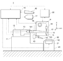
図1は、本実施形態に係るボンディング装置の構成図である。本実施形態に係るワイヤボンディング装置は、ワイヤボンディング工程を実施するために用いられる装置であり、一例として、本実施形態に係るワイヤボンディングの検査装置30を備えている。
FIG. 1 is a configuration diagram of a bonding apparatus according to the present embodiment. The wire bonding apparatus according to the present embodiment is an apparatus used for performing a wire bonding process, and includes the wire
図1に示すように、本実施形態に係るワイヤボンディング装置1は、制御装置10、基台11、XYテーブル12、ボンディングヘッド13、トーチ電極14、キャピラリ15、超音波ホーン16、ワイヤクランパ17、ワイヤテンショナ18、回転スプール19、ボンディングステージ20、ヒータ21、検査装置30、操作部40、ディスプレイ41、およびカメラ42等を備えて構成される。
As shown in FIG. 1, a
以下の実施形態では、ボンディング対象となる半導体デバイス(例えば半導体ダイ)やリードフレームに平行な平面をXY平面とし、XY平面に垂直な方向をZ方向とする。キャピラリ15の先端位置は、X座標、Y座標、およびZ座標で表される空間座標(X,Y,Z)で特定される。
In the following embodiments, a plane parallel to a semiconductor device (for example, a semiconductor die) or a lead frame to be bonded is an XY plane, and a direction perpendicular to the XY plane is a Z direction. The tip position of the
基台11は、XYテーブル12を摺動可能に載置して構成されている。XYテーブル12は、制御装置10からの駆動信号に基づいてキャピラリ15をXY平面で所定の位置に移動可能な移動装置である。
The
ボンディングヘッド13は、制御装置10からの駆動信号に基づいて超音波ホーン16をZ方向に移動可能に保持する移動装置である。ボンディングヘッド13は軽量な低重心構造を備えており、XYテーブル12の移動に伴って発生する慣性力によるキャピラリ15の動きを抑制可能に構成されている。
The bonding
超音波ホーン16は、末端から先端にかけて、末端部、フランジ部、ホーン部、および先端部の各部で構成された棒状部材である。末端部は、制御装置10からの駆動信号に応じて振動する超音波発振器161が配置されている。フランジ部は超音波振動の節となる位置でボンディングヘッド13に共振可能に取り付けられている。ホーン部は、末端部の径に比べて長く延在するアームであり、超音波発振器161による振動の振幅を拡大して先端部に伝える構造を備えている。先端部はキャピラリ15を交換可能に保持する取付部となっている。超音波ホーン16は全体として超音波発振器161の振動に共鳴する共振構造を備えており、共振時の振動の節に超音波発振器161およびフランジが位置し、振動の腹にキャピラリ15が位置するような構造に構成されている。これらの構成により、超音波ホーン16は電気的な駆動信号を機械的な振動に変換するトランスデューサとして機能する。
The
キャピラリ15は、ワイヤボンディングに用いられるボンディングツールである。キャピラリ15には、挿通穴が設けられており、ボンディングに使用するワイヤwが挿通され繰り出し可能に構成されている。キャピラリ15はバネ力等により交換可能に超音波ホーン16に取り付けられている。
The capillary 15 is a bonding tool used for wire bonding. The capillary 15 is provided with an insertion hole so that the wire w used for bonding can be inserted and fed out. The capillary 15 is attached to the
ワイヤクランパ17は、制御装置10の制御信号に基づいて開閉動作を行う電磁石構造を備えており、所定のタイミングでワイヤwを把持したり解放したりすることが可能なように構成されている。
The
ワイヤテンショナ18は、ワイヤwを挿通し、制御装置10の制御信号に基づいてワイヤwに対する張力を自在に変更することにより、ボンディング中のワイヤwに適度な張力を与えることが可能に構成されている。
The
回転スプール19は、ワイヤwが巻き回されたリールを交換可能に保持しており、ワイヤテンショナ18を通じて及ぼされる張力に応じてワイヤwを繰り出すように構成されている。なお、ワイヤwの材料は、加工の容易さと電気抵抗の低さから選択される。通常、金(Au)やアルミニウム(Al)や銅(Cu)等が用いられる。
The
トーチ電極14は、図示しない放電安定化抵抗を介して図示しない高電圧電源に接続されており、制御装置10からの制御信号に基づいてスパーク(放電)を発生し、スパークの熱によってキャピラリ15の先端から繰り出されているワイヤwの先端にボールを形成可能に構成されている。また、トーチ電極14の位置は固定されており、放電時にはキャピラリ15がトーチ電極14から所定の距離まで接近し、ワイヤwの先端とトーチ電極14との間で適度なスパークを発生するようになっている。
The
ボンディングステージ20は、ボンディング対象となる半導体デバイス50およびリードフレーム60を加工面に載置するステージである。ボンディングステージ20の加工面の下部にはヒータ21が設けられており、半導体デバイス50およびリードフレーム60をボンディングに適する温度にまで加熱可能に構成されている。
The
検査装置30は、本実施形態に係るワイヤボンディングの検査方法に用いられる装置である。検査装置30と制御装置10との間は、一方が他方の機能を作動又は停止させることができるよう信号の送受信が可能なように構成されている。
The
操作部40は、トラックボール、ジョイスティック、タッチパネル等の入力手段を備え、オペレータの操作内容を制御装置10に出力する入力装置である。カメラ42は、ボンディングステージ20の加工面に載置された半導体デバイス50やリードフレーム60を撮影可能に構成されている。ディスプレイ41は、カメラ42で撮像された画像をオペレータに視認可能な所定の倍率で表示するようになっている。オペレータはディスプレイ41に表示される半導体デバイス50の電極やリードフレーム60を観察しながら操作部40を操作してキャピラリ15の軌跡を設定していく。
The
制御装置10は、所定のソフトウェアプログラムに基づき当該ワイヤボンディング装置1を制御する各種制御信号を出力可能に構成されている。具体的には、制御装置10は限定のない例示として以下の制御を行う。
The
(1)図示しない位置検出センサからの検出信号に基づいてキャピラリ15の先端の空間位置(X,Y,Z)を特定し、上記プログラムにより規定される空間位置へキャピラリ15を移動させる駆動信号をXYテーブル12およびボンディングヘッド13に出力すること。
(1) A drive signal for specifying the spatial position (X, Y, Z) of the tip of the capillary 15 based on a detection signal from a position detection sensor (not shown) and moving the capillary 15 to a spatial position defined by the program. Output to the XY table 12 and the
(2)ボンディング点へのボンディング時に超音波振動を発生させる制御信号を超音波ホーン16の超音波発振器161に出力すること。
(2) A control signal for generating ultrasonic vibration at the time of bonding to the bonding point is output to the
(3)上記プログラムにより規定されるワイヤwの繰り出し量が、所定量となるようにワイヤクランパ17の開閉動作を制御する制御信号を出力すること。具体的にワイヤwを繰り出す際にはワイヤクランパ17を解放状態とし、ワイヤwに屈曲点を形成する場合または切断する場合にはワイヤクランパ17を拘束状態とする。
(3) To output a control signal for controlling the opening / closing operation of the
(4)ワイヤwの先端にボールを形成する時にトーチ電極14に放電させるための制御信号を出力すること。
(5)カメラ42からの画像をディスプレイ41に出力すること。
(6)操作部40の操作内容に基づいてボンディング点、屈曲点等の空間座標を特定すること。
(4) To output a control signal for causing the
(5) Output an image from the
(6) Specifying spatial coordinates such as bonding points and bending points based on the operation content of the
なお、上記ボンディング装置1の構成は例示であり、上記に限定されない。例えば、X方向、Y方向、またはZ方向に移動させる移動装置はボンディングステージ20側に設けてもよく、またボンディング装置1側およびボンディングステージ20側の双方に設けてもよい。
In addition, the structure of the said
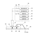
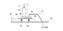
図2は、本実施形態に係るワイヤボンディングの検査装置を説明するための図である。この検査装置30は、半導体デバイス50とリードフレーム60とを電気的に接続するためのワイヤボンディングが正常に行われたか否か(ボンディング良否)を検査するものである。
FIG. 2 is a view for explaining the wire bonding inspection apparatus according to the present embodiment. The
半導体デバイス50の一方の面には、複数の電極52,54が形成されている。一般的に、半導体デバイス50は、それぞれの電極ごとに極性を有している。例えば、半導体デバイス50の基板部分がn型基板からなり、電極52,54がp型不純物領域上に形成された場合、半導体デバイス50は全体としてみると、基板側をカソードとし、電極側をアノードとしたダイオード53,55に相当する部分(以下、単に「ダイオード」という。)を備えていることになる。
A plurality of
リードフレーム60は、例えば銅などの金属からなる導電性フレームである。リードフレーム60は、ダイパッド62と、複数のインナーリード64と、複数のアウターリード(図2では省略してある。)との各部分を含み、それらの各部分は製造工程の段階(少なくともワイヤボンディング工程の段階)においては一体的に形成されて相互に電気的に接続された状態となっている。また、リードフレーム60はボンディングステージ(加工台)20に載置されており、少なくともワイヤボンディング工程中においては基準電位(例えば接地電位GND)に設定されている。
The
半導体デバイス50は、導電性接着剤(図示しない)を介して、リードフレーム60のダイパッド62にダイボンディングされており、半導体デバイス50の基板部分(半導体デバイス50の裏面)は、リードフレーム60と実質的に同電位となっている。ワイヤボンディング工程においては、半導体デバイス50の複数の電極と、リードフレーム60の複数のインナーリードとが相互に複数のワイヤによって結線され、一般的には、図2に示すように1つの電極54と1つのインナーリード64とが1つのワイヤ70によって電気的に接続される。
The
本実施形態に係るワイヤボンディングの検査装置30は、電圧供給手段32と、電圧検出手段34と、制御手段36と、判定手段38と、記憶手段39とを備える。
The wire
電圧供給手段32は、バッファ90及び電流制限抵抗92を介して、キャピラリ15によって保持されたワイヤwに印加電圧を供給するよう構成されている。電圧供給手段32は、直流電源を有する。すなわち、電圧供給手段32は、半導体デバイス50の基板部分とボンディングしようとする所定の電極52との間に形成されるダイオード53の極性に応じて、ワイヤwに正電圧又は負電圧を供給する。
The voltage supply means 32 is configured to supply an applied voltage to the wire w held by the capillary 15 via the
電圧検出手段34は、電圧供給手段32の印加電圧に応じて、電流制限抵抗94及びバッファ96を介して、キャピラリ15によって保持されたワイヤwから流れる電流に基づく電圧値を検出するよう構成されている。
The
制御手段36は、電圧供給手段32の印加電圧の電圧値(正負の向きや大きさ)及び印加電圧の供給タイミングなどを制御するよう構成されている。制御手段36は、制御装置10によるワイヤボンディングの処理に連動して、予め決められたプログラムに基づいて電圧供給手段32の動作を制御する。なお、印加電圧の電圧値や印加電圧の供給タイミングの初期設定は、装置操作者による手入力によって行うことができる。
The control means 36 is configured to control the voltage value (positive and negative direction and magnitude) of the applied voltage of the voltage supply means 32, the supply timing of the applied voltage, and the like. The
判定手段38は、電圧検出手段34によって検出された電圧値に基づいて、ワイヤボンディングの処理が正常に行われたか否か(ボンディング良否)を判定するよう構成されている。具体的には、判定手段38は、電圧供給手段32からの印加電圧に関するデータ、電圧検出手段34からの検出電圧に関するデータ、及び、ワイヤボンディングを制御する制御装置10からのワイヤボンディングの処理に関するデータ(例えばキャピラリ15のZ位置及び時間の各データ)に基づいて、ボンディング良否を判定する。判定手段38による判定結果は、例えばディスプレイ(図示しない)に表示することによって装置操作者が視認できるように構成されていてもよい。また、判定手段38による判定結果のデータは、ワイヤボンディングを制御する制御装置10へ送信され、この判定結果のデータに基づいて、制御装置10がワイヤボンディング工程を継続又は停止するように構成されていてもよい。
The
記憶手段39は、検査装置30の上記各手段のデータを格納するものである。例えば、記憶手段39に格納されたデータに基づいて、制御手段32による制御が行われてもよい。例えば、ダイオードの極性が同じタイプの半導体デバイスごとに、電圧供給手段32の印加電圧の電圧値(正負の向きや大きさ)及び印加電圧の供給タイミングなどのデータを記憶手段39に予め格納しておき、このような事前データを用いてワイヤボンディングの検査を行ってもよい。
The storage means 39 stores the data of each means of the
次に、本実施形態に係るワイヤボンディングの検査方法について説明する。以下の例では、上記したワイヤボンディング装置1を使用してワイヤボンディングの検査を行う。
Next, a wire bonding inspection method according to this embodiment will be described. In the following example, wire bonding inspection is performed using the
まず、ワイヤボンディング装置1の基本的な動作について説明する。
First, the basic operation of the
最初にすべきことは、制御装置10に、ワイヤwの形状(始点、屈曲点、終点等)を規定するキャピラリ15の先端の軌跡を設定点として記録することである。ボンディングステージ20には、ボンディング対象物、例えば、半導体デバイス50およびリードフレーム60が載置される。ワイヤボンディング始点は、半導体デバイス50の電極52であり、終点はリードフレーム60のインナーリード65である。またワイヤwを拘束した状態でキャピラリ15の移動方向を変更する設定点を記録することにより、屈曲点を含んだループが形成される。
The first thing to do is to record in the
オペレータはカメラ42で撮像された画像をディスプレイ41にて観察しながら操作部40を操作して、設定点の空間座標を記録していく。具体的には、操作部40から座標情報を入力したりディスプレイ41に表示されるマーカを所望の点に位置させて入力したりすることで、その点のX座標およびY座標を記録する。基準面(例えばリードフレーム60の表面)からのZ方向の変位を操作部40から数値入力することで、Z座標を記録する。
The operator operates the
ボンディング対象となる総てのワイヤwに対して上記設定点の空間座標の記録を行ってからボンディング動作を開始させる。制御装置10は、記録された設定点の順番に従ってキャピラリ15を、半導体デバイス50およびリードフレーム60に対して相対的に移動させ、ワイヤクランパ17による解放および把持を繰り返しながら記録された軌跡に沿ってキャピラリ15を移動させてボンディング動作を実行する。
After the spatial coordinates of the set points are recorded for all the wires w to be bonded, the bonding operation is started. The
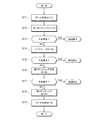
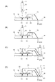
図3〜図7は、本実施形態のワイヤボンディングの検査方法を説明するための図である。ここで、図3は、ワイヤボンディングの検査方法についてのフローチャートであり、図4(A)〜(D)はワイヤボンディングが正常に行われた場合の一例を示し、図5及び図6はワイヤボンディング不良が発生した場合の一例を示したものである。 3-7 is a figure for demonstrating the inspection method of the wire bonding of this embodiment. Here, FIG. 3 is a flowchart of a method for inspecting wire bonding. FIGS. 4A to 4D show an example in which wire bonding is normally performed, and FIGS. 5 and 6 show wire bonding. An example when a defect occurs is shown.
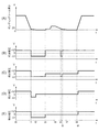
また、図7(A)〜(E)は、ワイヤボンディングの検査方法についてのタイミングチャートである。具体的には、図7(A)がボンディングツール(すなわちキャピラリの先端のZ位置)の軌跡を示し、図7(B)が電圧供給手段の印加電圧を示し、図7(C)〜(E)が電圧検出手段の検出電圧を示したものである。ここで、図7(C)はワイヤボンディングが正常に行われた場合のタイミングチャートであり、図7(D)及び(E)はワイヤボンディング不良が発生した場合のタイミングチャートである。なお、図7(D)及び(E)においては、ワイヤボンディング不良が発生した時間以降、ワイヤボンディング工程を停止することなく継続した場合の検出電圧値を図示している。 7A to 7E are timing charts for the wire bonding inspection method. Specifically, FIG. 7A shows the locus of the bonding tool (that is, the Z position of the tip of the capillary), FIG. 7B shows the applied voltage of the voltage supply means, and FIGS. ) Shows the detection voltage of the voltage detection means. Here, FIG. 7C is a timing chart when the wire bonding is normally performed, and FIGS. 7D and 7E are timing charts when the wire bonding failure occurs. 7D and 7E show the detected voltage values when the wire bonding process is continued without stopping after the time when the wire bonding failure occurs.
以下、これらの図3〜図7を参照しつつ、本実施形態のワイヤボンディングの検査方法の一例について説明する。以下においては、リードフレーム60の基準電位を接地電位(GND)とし、半導体デバイス50の基板部分とボンディングしようとする電極52との間に基板側をカソードとし、電極側をアノードとしたダイオード53が形成されている場合を例に説明する。なお、図3のフローチャート中に記載された時間t0〜t9は、図7(A)〜(E)の横軸の時間t0〜t9に対応している。
Hereinafter, an example of the wire bonding inspection method of this embodiment will be described with reference to FIGS. In the following description, a
<時間t0からt1まで>
図3に示すように、まず、ワイヤwの先端にボールを形成する(S11)。すなわち、キャピラリ15の先端から延出したワイヤの一部を所定の高電圧に印加されたトーチ電極14(図1参照)に近づけて、当該ワイヤの一部とトーチ電極14との間で放電を発生させる。こうして、図4(A)に示すように、当該ワイヤの先端が表面張力によって溶融したフリーエアーボール81を形成する。ワイヤwの先端にフリーエアーボール81を形成したら、キャピラリ15を、これからボンディングしようとする半導体デバイス50の電極52に向かって下降させる。
<From time t0 to t1>
As shown in FIG. 3, first, a ball is formed at the tip of the wire w (S11). That is, a part of the wire extending from the tip of the capillary 15 is brought close to the torch electrode 14 (see FIG. 1) applied with a predetermined high voltage, and a discharge is caused between the part of the wire and the
図7(B)に示すように、時間t0からt1までの期間において、電圧供給手段32は、キャピラリ15に保持されたワイヤwに印加電圧+Vを供給する。すなわち、半導体デバイス50における、これからボンディングしようとする電極52に対応するダイオード53に順方向に電流が流れる向きの電圧と同極性である正電圧を供給する。この場合、ワイヤwは電極52はもとより他の導電部材とは電気的に導通していない状態であるから、図7(C)〜(E)に示すように、電圧検出手段34は、印加電圧+Vと同様、検出電圧+Vを検出することになる。
As shown in FIG. 7B, in the period from time t0 to t1, the voltage supply means 32 supplies the applied voltage + V to the wire w held by the capillary 15. That is, a positive voltage having the same polarity as a voltage in a direction in which a current flows in the forward direction is supplied to the
なお、本実施形態においては、図4(A)に示すように、時間t0よりも前において、半導体デバイス50の他の電極54(電極52に隣接する電極)が、ワイヤ70を介してリードフレーム60と電気的に接続されており、これにより半導体デバイス50の電極54がGNDに接続された状態となっている。これによって、仮に、ワイヤwが、電極54、デフォームドボール72及びワイヤ70のいずれかに接触した場合には、ワイヤwからGNDの向き又はGNDからワイヤwの向きに電流が流れ得るようになっている。
In the present embodiment, as shown in FIG. 4A, the other electrode 54 (electrode adjacent to the electrode 52) is connected to the lead frame via the
<時間t1からt3まで>
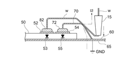
次に、図3に示すように、第1ボンディングを行う(S12)。第1ボンディングのボンディング地点は、半導体デバイス50の電極52である。キャピラリ15が下降することによって、時間t1においてフリーエアーボール81が電極52に当接し始め、その後時間t2からt3にかけて、フリーエアーボール81が、キャピラリ15に付与されている荷重によりさらに変形する。なお、フリーエアーボール81が第1ボンディングのボンディング地点でボンディングされた後は、フリーエアーボール81はデフォームドボール82になる。このとき、制御装置10は超音波ホーン16に制御信号を供給して超音波発振器161に超音波振動を発生させ、超音波ホーン16及びキャピラリ15を介して、デフォームドボール82に超音波振動を加える。また、半導体デバイス50の電極52は、ヒータ21により所定の熱が加えられているので、デフォームドボール82に加えられている荷重、超音波振動、及びヒータ21により加えられている熱の相互作用によって、デフォームドボール82が電極52にボンディングされる。
<From time t1 to t3>
Next, as shown in FIG. 3, first bonding is performed (S12). The bonding point of the first bonding is the
図7(B)に示すように、時間t1からt3までの期間、電圧供給手段32は、ワイヤwに印加電圧−V1を供給する。すなわち、半導体デバイス50における、これからボンディングしようとする電極52に対応するダイオード53に順方向に電流が流れる向きの電圧とは逆極性である負電圧を供給する。そして、本期間において、ボンディング不良が発生していないかどうかを判定するための、第1の態様によるボンディング良否の検査を行う(S13)。
As shown in FIG. 7B, the voltage supply means 32 supplies the applied voltage −V1 to the wire w during the period from time t1 to t3. That is, a negative voltage having a polarity opposite to the voltage in the direction in which a current flows in the forward direction is supplied to the
(ボンディングが正常である場合)
図4(B)に示すように、デフォームドボール82が、ボンディングしようとする電極52に正確にボンディングされた場合、印加電圧−V1とGNDとの間の電位差により、ダイオード53に逆方向のバイアスが加えられるので、ダイオード53を介して電流が流れることはない。またそれ以外に電流が流れる経路は存在していない。したがって、図7(C)に示すように、時間t1からt3までの期間において、電圧検出手段34は、印加電圧と同一の電圧値−V1を検出することになる。こうして、判定手段38は、かかる検出電圧値に基づいて、時間t1からt3までの期間のワイヤボンディング工程が正常に行われたことを判定する。
(When bonding is normal)
As shown in FIG. 4B, when the
(ボンディング不良が発生した場合)
他方、図5に示すように、デフォームドボール82が、ボンディングしようとする電極52からXY位置がずれてボンディングされ、これによって、デフォームドボール82が隣接する電極54及び/又はデフォームドボール72に接触した場合、印加電圧−V1とGNDとの間の電位差により、GNDからワイヤ70を介してキャピラリ15に保持されたワイヤwに電流I1が流れる。したがって、図7(D)に示すように、電圧検出手段34は、時間t2からt3までの期間において、電流I1に基づく電圧値0Vを検出することになる。こうして、判定手段38は、かかる検出電圧値に基づいて、時間t2からt3までの期間にボンディング不良が発生したことを判定する。
(When a bonding failure occurs)
On the other hand, as shown in FIG. 5, the
なお、時間t1からt2までの期間は、未だ第1ボンディングし始めの期間であり、デフォームドボール82に荷重が十分に加えられる前の段階である。したがって、判定手段38は、時間t2からt3の期間(すなわち、デフォームドボール82に荷重が加えられている期間)における検出電圧値に基づいて、ボンディング良否を判定することが好ましい。
The period from the time t1 to the time t2 is still a period during which the first bonding is started, and is a stage before a sufficient load is applied to the
図3に示すように、ボンディング良否の検査の結果、ボンディング不良が発生したと判定された場合(S13 YES)には、検査装置30は、制御装置10に対して、ワイヤボンディングの処理を一旦停止するよう命令する。こうして、ボンディング不良が発生した半導体デバイス50は、ワイヤボンディングの製造ラインから外されて例えば廃棄されてもよい。制御装置10は、検査装置30からのボンディング不良があったことを示す信号を受信したことに基づいて、直ちにワイヤボンディングの処理を停止してもよいし、あるいは、直ちに停止しなくてもその後のいずれかのタイミング(例えば、処理中の電極52に対する一連のワイヤボンディング工程を終えるタイミング(時間t9以降))にワイヤボンディングの処理を停止してもよい。他方、ボンディングが正常に行われたと判定された場合(S13 NO)には、その後のワイヤボンディングの工程が続行される。
As shown in FIG. 3, when it is determined that a bonding failure has occurred as a result of the bonding quality test (YES in S13), the
<時間t3からt5まで>
次に、図3に示すように、ワイヤwを、第2ボンディング地点であるリードフレーム60のインナーリード65に向けてループする(S14)。具体的には、ワイヤクランパ17を開放状態にしてキャピラリ15の先端からワイヤwを繰り出しながら、キャピラリ15を第1ボンディング地点である電極52から上昇させ、その後、キャピラリ15をリードフレーム60のインナーリード65に向かって所定の軌跡に沿って移動させる。キャピラリ15が描く所定の軌跡は、例えば図7(A)の時間t3からt5のチャートを参照することができる。
<From time t3 to t5>
Next, as shown in FIG. 3, the wire w is looped toward the
図7(B)に示すように、時間t3からt5までの期間、電圧供給手段32は、ワイヤwに印加電圧+Vを供給する。すなわち、半導体デバイス50における、ボンディング済みの電極52に対応するダイオード53に順方向に電流が流れる向きの電圧と同極性である正電圧を供給する。そして、本期間において、ボンディング不良が発生していないかどうかを判定するための、第2の態様によるボンディング良否の検査を行う(S15)。
As shown in FIG. 7B, the voltage supply means 32 supplies the applied voltage + V to the wire w during the period from time t3 to t5. That is, a positive voltage having the same polarity as the voltage in the direction in which a current flows in the forward direction is supplied to the
(ボンディングが正常である場合)
時間t3からt5までワイヤwをループさせる期間において、デフォームドボール82と電極52とが電気的に接続された状態が維持されていれば、印加電圧+V1とGNDとの間の電位差により、ダイオード53に順方向のバイアスが加えられるので、ワイヤwからダイオード53を介してGNDの方向に電流が流れる。したがって、図7(C)に示すように、時間t3からt5までの期間において、電圧検出手段34は上記電流に基づく電圧値0Vを検出することになる。こうして、判定手段38は、かかる検出電圧値に基づいて、時間t3からt5までの期間のワイヤボンディング工程が正常に行われたことを判定する。
(When bonding is normal)
If the
(ボンディング不良が発生した場合)
他方、時間t3からt5までワイヤwをループさせる期間において、デフォームドボール82が電極52から剥離してしまうと、ワイヤwは電極52とは電気的に導通していない状態となるから、電圧検出手段34は、印加電圧+Vと同様、検出電圧+Vを検出することになる(図示しない)。こうして、判定手段38は、かかる検出電圧値に基づいて、時間t3からt5までの期間(少なくも時間t4からt5までの期間)にボンディング不良が発生したことを判定する。
(When a bonding failure occurs)
On the other hand, if the
図3に示すように、ボンディング良否の結果、ボンディング不良が発生したと判定された場合(S15 YES)には、検査装置30は、制御装置10に対して、ワイヤボンディングの処理を一旦停止するよう命令する。なお、制御装置10によるワイヤボンディングの処理の停止のタイミングについては、時間t1からt3までの期間での説明と同様である。他方、ボンディングが正常に行われたと判定された場合(S15 NO)には、その後のワイヤボンディングの工程が続行される。
As shown in FIG. 3, when it is determined that bonding failure has occurred as a result of the bonding quality (YES in S15), the
<時間t5からt6まで>
次に、図3に示すように、第2ボンディング直前の状態に移行する(S16)。すなわち、図4(C)に示すように、キャピラリ15を操作することによって、ワイヤwの一部(キャピラリ15の先端から延出した一部)を、第2ボンディング地点であるリードフレーム60のインナーリード65の上方(キャピラリ15の先端の高さZ5)まで移動させる。この段階では、ワイヤwの一部は、まだインナーリード65とは電気的に導通していない状態である。時間t5からt6までの期間は、図4(C)に示すように、キャピラリ15は、リードフレーム60に向かって下降途中であってもよいし、あるいは、時間t5からt6のいずれかの時間において一時的にその移動をストップさせてもよい。
<From time t5 to t6>
Next, as shown in FIG. 3, the state immediately before the second bonding is shifted (S16). That is, as shown in FIG. 4C, by operating the capillary 15, a part of the wire w (a part extending from the tip of the capillary 15) is transferred to the inner side of the
図7(B)に示すように、時間t5からt6までの期間、電圧供給手段32は、ワイヤwに印加電圧−V1を供給する。すなわち、半導体デバイス50における、ボンディング済みの電極52に対応するダイオード53に順方向に電流が流れる向きとは逆極性である負電圧を供給する。そして、本期間において、ボンディング不良が発生していないかどうかを判定するための、第3の態様によるボンディング良否の検査を行う(S17)。
As shown in FIG. 7B, the voltage supply means 32 supplies the applied voltage −V1 to the wire w during the period from time t5 to t6. That is, a negative voltage having a polarity opposite to the direction in which a current flows in the forward direction is supplied to the
(ボンディングが正常である場合)
図4(C)に示すように、電極52に接続されたワイヤwが、所望のループ形状を有しており、他の隣接するワイヤ70とは接触していない場合、印加電圧−V1とGNDとの間の電位差により、ダイオード53に逆方向のバイアスが加えられるので、ダイオード53を介して電流が流れることはない。またそれ以外に電流が流れる経路は存在していない。したがって、図7(C)に示すように、時間t5からt6までの期間において、電圧検出手段34は、印加電圧と同一の電圧値−V1を検出することになる。こうして、判定手段38は、かかる検出電圧値に基づいて、時間t5からt6までの期間のワイヤボンディング工程が正常に行われたことを判定する。
(When bonding is normal)
As shown in FIG. 4C, when the wire w connected to the
(ボンディング不良が発生した場合)
他方、図6に示すように、電極52に接続されたワイヤwが、所望のループ形状からXYZ位置がずれてループされ、他の隣接するワイヤ70に接触した場合、印加電圧−V1とGNDとの間の電位差により、GNDからワイヤ70を介してキャピラリ15に保持されたワイヤwに電流I2が流れる。したがって、図7(E)に示すように、電圧検出手段34は、時間t5からt6までの期間において、電流I2に基づく電圧値0Vを検出することになる。こうして、判定手段38は、かかる検出電圧値に基づいて、時間t5からt6までの期間にボンディング不良が発生したことを判定する。
(When a bonding failure occurs)
On the other hand, as shown in FIG. 6, when the wire w connected to the
ボンディング良否の検査の結果、ボンディング不良が発生したと判定された場合(S17 YES)には、検査装置30は、制御装置10に対して、ワイヤボンディングの処理を一旦停止するよう命令する。なお、制御装置10によるワイヤボンディングの処理の停止のタイミングについては、時間t1からt3までの期間での説明と同様である。他方、ボンディングが正常に行われたと判定された場合(S17 NO)には、その後のワイヤボンディングの工程が続行される。
If it is determined that bonding failure has occurred as a result of the bonding quality test (YES in S17), the
<時間t6からt8まで> 次に、図3に示すように、第2ボンディングを行う(S18)。すなわち、第2ボンディング地点であるリードフレーム60のインナーリード65に、ワイヤwの一部をボンディングする。具体的には、キャピラリ15が下降することによって、時間t6においてワイヤwの一部がインナーリード65に当接し始め、その後、時間t7からt8にかけて、ワイヤwの一部が、キャピラリ15に付与されている荷重により変形する。このとき、制御装置10は超音波ホーン16に制御信号を供給して超音波発振器161に超音波振動を発生させ、超音波ホーン16及びキャピラリ15を介して、ワイヤwに超音波振動を加える。また、リードフレーム60は、ヒータ21により所定の熱が加えられているので、ワイヤwに加えられている荷重、超音波振動、及びヒータ21により加えられている熱の相互作用によって、ワイヤwの一部がリードフレーム60のインナーリード65にボンディングされる。
<From time t6 to t8> Next, as shown in FIG. 3, second bonding is performed (S18). That is, a part of the wire w is bonded to the
図7(B)に示すように、時間t7からt8までの期間、電圧供給手段32は、ワイヤwに印加電圧+Vを供給する。すなわち、半導体デバイス50における、ボンディング済みの電極52に対応するダイオード53に順方向に電流が流れる向きの電圧と同極性である正電圧を供給する。なお、この場合、ワイヤwが電極52及びインナーリード65のいずれかに電気的に接続された状態が維持されていれば、印加電圧+V1とGNDとの間の電位差により、ワイヤwからGNDの方向に電流が流れて、図7(C)に示すように、電圧検出手段34は上記電流に基づく電圧値0Vを検出することになる。
As shown in FIG. 7B, the voltage supply means 32 supplies the applied voltage + V to the wire w during the period from time t7 to t8. That is, a positive voltage having the same polarity as the voltage in the direction in which a current flows in the forward direction is supplied to the
<時間8からt9まで>
その後、図3に示すように、ワイヤwを切断する(S19)。具体的には、制御装置10はワイヤクランパ17に制御信号を供給してワイヤwを拘束状態としてから、ボンディングヘッド13に駆動信号を供給してキャピラリ15を引き上げる。図4(D)に示すように、リードフレーム60へボンディングされた状態で強制的に引っ張られ張力が印加されると、ワイヤwの一部に破断が生じる(テールカット)。こうして、半導体デバイス50の電極52と、リードフレーム60のインナーリード65とは、ワイヤ80及びデフォームドボール82を介して電気的に接続され、半導体デバイス50の電極52に対するワイヤボンディング工程が終了する。その後、上記したS11からS19までの各検査工程を、半導体デバイス50の次の電極に対するワイヤボンディング工程について繰り返し行う。
<From time 8 to t9>
Thereafter, as shown in FIG. 3, the wire w is cut (S19). Specifically, the
以上のとおり、本実施形態によれば、ワイヤボンディング工程のときに、ワイヤwに供給した印加電圧に対する検出電圧値の変化を検出することによってボンディング良否を検査する。したがって、ボンディング良否を効率良く判定することができる。また、電圧値の変化を検出することによってワイヤの短絡や接触不良などの様々な態様のワイヤボンディング不良を検査することができるので、ボンディング良否を容易かつ確実に判定することができる。 As described above, according to the present embodiment, bonding quality is inspected by detecting a change in the detected voltage value with respect to the applied voltage supplied to the wire w during the wire bonding step. Therefore, the quality of bonding can be determined efficiently. In addition, by detecting a change in the voltage value, it is possible to inspect various types of wire bonding defects such as wire short-circuiting or contact failure, so that bonding quality can be determined easily and reliably.
本発明は、上記実施形態に限定されることなく種々に変形して適用することが可能である。 The present invention is not limited to the above-described embodiment, and can be variously modified and applied.
例えば、上記実施形態では、ボンディングしようとする電極52に対応するダイオード53として、基板側をカソードとし、電極側をアノードとした向きのダイオードを示したが、例えば、基板側をアノードとし、電極側をカソードとした向きのダイオードを用いてもよい。この場合においても、上記実施形態の内容に接した当業者であれば、上記実施形態とは逆向きの印加電圧をワイヤに供給し、当該印加電圧に対する検出電圧値の変化を検出することによって、上記実施形態で説明したいずれかのボンディング良否を検査することができると理解できるものである。
For example, in the above-described embodiment, the
また、上記実施形態では、他の電極54がワイヤ70を介してリードフレーム60と電気的に接続された例を説明したが、必ずしも、他の電極54は既にワイヤボンディングがなされる必要はない。例えば、電極54は、当該電極54に対応するダイオードが基板側をアノードとし、電極側をカソードとした向きに形成されることによって、ワイヤが形成されていなくても、リードフレームから当該ダイオードを介して電極54の向きに順方向に電流が流れ得るようになっていればよい。
In the above-described embodiment, the example in which the
また、リードフレーム60の基準電位は、必ずしも接地電位GNDでなくてもよく、ある値をもった電圧値を基準としてもよい。この場合に、印加電圧及び検出電圧の電圧値は、基準電位の電圧値、及び、ボンディングしようとする電極に対応するダイオードの極性に基づいて上記説明した内容の趣旨を逸脱しない範囲で自由に設定可能であることは上記実施形態の内容に接した当業者であれば理解できるものである。
Further, the reference potential of the
また、上記実施形態では、第1ボンディングの前にワイヤwの先端にボールを形成する工程を含む例を説明したが、上記ボール形成工程は省略してもよい。例えば、ワイヤの材料としてアルミニウムを用いた場合はボールを形成することなく、ワイヤの一部を第1ボンディングしてもよい。 Moreover, although the said embodiment demonstrated the example including the process of forming a ball | bowl at the front-end | tip of the wire w before 1st bonding, you may abbreviate | omit the said ball | bowl formation process. For example, when aluminum is used as the wire material, a part of the wire may be first bonded without forming a ball.
上記発明の実施形態を通じて説明された実施例や応用例は、用途に応じて適宜に組み合わせて、又は変更若しくは改良を加えて用いることができ、本発明は上述した実施形態の記載に限定されるものではない。そのような組み合わせ又は変更若しくは改良を加えた形態も本発明の技術的範囲に含まれ得ることが、特許請求の範囲の記載から明らかである。 The examples and application examples described through the embodiments of the present invention can be used in combination as appropriate according to the application, or can be used with modifications or improvements, and the present invention is limited to the description of the above-described embodiments. It is not a thing. It is apparent from the description of the scope of claims that the embodiments added with such combinations or changes or improvements can be included in the technical scope of the present invention.
15…ボンディングツール(キャピラリ)、30…ワイヤボンディングの検査装置、32…電圧供給手段、34…電圧検出手段、50…半導体デバイス、60…リードフレーム、52,54…電極、53…ダイオード
DESCRIPTION OF
Claims (7)
(a)先端からワイヤの一部が延出しているボンディングツールを、前記半導体デバイスの複数の電極のうちの所定電極に向かって下降させること、
(b)前記ワイヤの一部を、前記半導体デバイスの前記所定電極にボンディングすること、
(c)前記ボンディングツールの先端から前記ワイヤを繰り出しながら前記ボンディングツールを所定の軌跡に沿って移動させて、前記ボンディングツールの先端から延出された前記ワイヤの一部を、前記リードフレームのリード部分の上方まで移動させること、
(d)前記ワイヤの一部を、前記リードフレームの前記リード部分にボンディングすること、
(e)前記ワイヤを切断すること
を含み、
前記検査方法は、さらに、(f)前記(b)及び/又は前記(c)のときに、前記ワイヤに、前記半導体デバイスの基板部分とボンディングしようとする前記所定電極との間のダイオードに相当する部分に順方向に電流が流れる向きの電圧とは逆極性の印加電圧を供給することを含み、
前記(f)において、前記印加電圧と前記リードフレームの前記基準電位との間の電位差に応じて流れる電流に基づく電圧値を検出することによってボンディング良否を検査することを特徴とするワイヤボンディングの検査方法。 An inspection method for wire bonding in which a lead frame set at a reference potential and a semiconductor device mounted on the lead frame are electrically connected by a wire,
(A) lowering a bonding tool in which a part of the wire extends from the tip toward a predetermined electrode of the plurality of electrodes of the semiconductor device;
(B) bonding a part of the wire to the predetermined electrode of the semiconductor device;
(C) moving the bonding tool along a predetermined trajectory while feeding the wire from the tip of the bonding tool so that a part of the wire extended from the tip of the bonding tool Moving to above the part,
(D) bonding a portion of the wire to the lead portion of the lead frame;
(E) cutting the wire;
The inspection method further corresponds to (f) a diode between the wire and the predetermined electrode to be bonded to the substrate portion of the semiconductor device in (b) and / or (c). Including supplying an applied voltage having a polarity opposite to a voltage in a direction in which a current flows in a forward direction to the portion to be
In (f), the bonding quality is inspected by detecting a voltage value based on a current flowing according to a potential difference between the applied voltage and the reference potential of the lead frame. Method.
前記ワイヤボンディングは、
(a)先端からワイヤの一部が延出しているボンディングツールを、前記半導体デバイスの複数の電極のうちの所定電極に向かって下降させること、
(b)前記ワイヤの一部を、前記半導体デバイスの前記所定電極にボンディングすること、
(c)前記ボンディングツールの先端から前記ワイヤを繰り出しながら前記ボンディングツールを所定の軌跡に沿って移動させて、前記ボンディングツールの先端から延出された前記ワイヤの一部を、前記リードフレームのリード部分の上方まで移動させること、
(d)前記ワイヤの一部を、前記リードフレームの前記リード部分にボンディングすること、
(e)前記ワイヤを切断すること
によって行われ、
前記検査装置は、
前記ワイヤに印加電圧を供給する電圧供給手段と、
前記ワイヤを介して流れる電流に基づく電圧値を検出する電圧検出手段と
を備え、
前記電圧供給手段は、前記(b)及び/又は前記(c)のときに、前記ワイヤに、前記半導体デバイスの基板部分とボンディングしようとする前記所定電極との間のダイオードに相当する部分に順方向に電流が流れる向きの電圧とは逆極性の印加電圧を供給するように構成され、
前記電圧検出手段は、ボンディング良否を検査するために、前記印加電圧と前記リードフレームの前記基準電位との間の電位差に応じて流れる電流に基づく電圧値を検出することを特徴とする、ワイヤボンディングの検査装置。 A wire bonding inspection apparatus that electrically connects a lead frame set to a reference potential and a semiconductor device mounted on the lead frame by a wire,
The wire bonding is
(A) lowering a bonding tool in which a part of the wire extends from the tip toward a predetermined electrode of the plurality of electrodes of the semiconductor device;
(B) bonding a part of the wire to the predetermined electrode of the semiconductor device;
(C) moving the bonding tool along a predetermined trajectory while feeding the wire from the tip of the bonding tool so that a part of the wire extended from the tip of the bonding tool Moving to above the part,
(D) bonding a portion of the wire to the lead portion of the lead frame;
(E) by cutting the wire;
The inspection device includes:
Voltage supply means for supplying an applied voltage to the wire;
Voltage detecting means for detecting a voltage value based on a current flowing through the wire,
In the case of (b) and / or (c), the voltage supply means is arranged in order in a portion corresponding to a diode between the substrate portion of the semiconductor device and the predetermined electrode to be bonded to the wire. It is configured to supply an applied voltage having a polarity opposite to the voltage in the direction in which current flows in the direction,
The wire detection unit detects a voltage value based on a current flowing according to a potential difference between the applied voltage and the reference potential of the lead frame in order to check bonding quality. Inspection equipment.
Priority Applications (2)
| Application Number | Priority Date | Filing Date | Title |
|---|---|---|---|
| JP2013257352A JP2015114242A (en) | 2013-12-12 | 2013-12-12 | Wire bonding inspection method and wire bonding inspection device |
| KR1020140147354A KR101643247B1 (en) | 2013-12-12 | 2014-10-28 | Method for testing wire bonding and apparatus for testing wire bonding |
Applications Claiming Priority (1)
| Application Number | Priority Date | Filing Date | Title |
|---|---|---|---|
| JP2013257352A JP2015114242A (en) | 2013-12-12 | 2013-12-12 | Wire bonding inspection method and wire bonding inspection device |
Publications (1)
| Publication Number | Publication Date |
|---|---|
| JP2015114242A true JP2015114242A (en) | 2015-06-22 |
Family
ID=53516226
Family Applications (1)
| Application Number | Title | Priority Date | Filing Date |
|---|---|---|---|
| JP2013257352A Pending JP2015114242A (en) | 2013-12-12 | 2013-12-12 | Wire bonding inspection method and wire bonding inspection device |
Country Status (2)
| Country | Link |
|---|---|
| JP (1) | JP2015114242A (en) |
| KR (1) | KR101643247B1 (en) |
Cited By (1)
| Publication number | Priority date | Publication date | Assignee | Title |
|---|---|---|---|---|
| CN110736938A (en) * | 2019-10-23 | 2020-01-31 | 中国电子科技集团公司第四十四研究所 | A detection structure and method for judging whether wire bonding is short-circuited |
Families Citing this family (2)
| Publication number | Priority date | Publication date | Assignee | Title |
|---|---|---|---|---|
| KR101964040B1 (en) * | 2018-01-05 | 2019-11-14 | (주)한중엔시에스 | Continuous automated manufacturing system of brush holder |
| CN112997307B (en) * | 2019-03-13 | 2024-06-18 | 株式会社新川 | Wire bonding failure detection system, detection device and detection method |
Family Cites Families (4)
| Publication number | Priority date | Publication date | Assignee | Title |
|---|---|---|---|---|
| JPS6384132A (en) | 1986-09-29 | 1988-04-14 | Toshiba Corp | Method and apparatus for inspecting wire bonding |
| JP4530984B2 (en) * | 2005-12-28 | 2010-08-25 | 株式会社新川 | Wire bonding apparatus, bonding control program, and bonding method |
| JP4467631B1 (en) * | 2009-01-07 | 2010-05-26 | 株式会社新川 | Wire bonding method |
| KR101620351B1 (en) * | 2012-01-30 | 2016-05-12 | 삼성전자주식회사 | Wire bonding method of electric element |
-
2013
- 2013-12-12 JP JP2013257352A patent/JP2015114242A/en active Pending
-
2014
- 2014-10-28 KR KR1020140147354A patent/KR101643247B1/en not_active Expired - Fee Related
Cited By (1)
| Publication number | Priority date | Publication date | Assignee | Title |
|---|---|---|---|---|
| CN110736938A (en) * | 2019-10-23 | 2020-01-31 | 中国电子科技集团公司第四十四研究所 | A detection structure and method for judging whether wire bonding is short-circuited |
Also Published As
| Publication number | Publication date |
|---|---|
| KR20150068896A (en) | 2015-06-22 |
| KR101643247B1 (en) | 2016-07-27 |
Similar Documents
| Publication | Publication Date | Title |
|---|---|---|
| KR101672510B1 (en) | Wire bonding device and wire bonding method | |
| CN102272911B (en) | Lead welding device and welding method | |
| US9899348B2 (en) | Wire bonding apparatus and method of manufacturing semiconductor device | |
| JP6067951B1 (en) | Wire bonding equipment | |
| CN103208436B (en) | The method of resetkey locking device from bonding fault | |
| US20160358883A1 (en) | Bump forming method, bump forming apparatus, and semiconductor device manufacturing method | |
| US10410992B2 (en) | Ball forming device, wire-bonding apparatus, and ball formation method | |
| CN102024722B (en) | Lead soldering method | |
| JP2015114242A (en) | Wire bonding inspection method and wire bonding inspection device | |
| TW201503272A (en) | Method and apparatus for measuring airless ball size during wire bonding | |
| US12107067B2 (en) | Wire bonding device, wire cutting method and non-transitory computer-readable recording medium recording program | |
| CN106463423B (en) | Discharge inspection device, wire bonding device, and discharge inspection method | |
| TWI811074B (en) | Bonding apparatus and alignment method | |
| TWI831248B (en) | Bump forming device, bump forming method and bump forming computer program product | |
| JP5338759B2 (en) | Wire bonding method | |
| JP7515216B1 (en) | Wire bonding apparatus and recovery method | |
| JP2015156469A (en) | Bump formation method, bump formation device, and method for manufacturing semiconductor device | |
| JP2010147328A (en) | Load detection device, bonding device, and load detection method | |
| JP2007116022A (en) | Bonding apparatus and bonding method | |
| JPH06140458A (en) | Wire bonding equipment |