JP2015103244A - Touch sensor module and method for manufacturing the same - Google Patents
Touch sensor module and method for manufacturing the same Download PDFInfo
- Publication number
- JP2015103244A JP2015103244A JP2014195823A JP2014195823A JP2015103244A JP 2015103244 A JP2015103244 A JP 2015103244A JP 2014195823 A JP2014195823 A JP 2014195823A JP 2014195823 A JP2014195823 A JP 2014195823A JP 2015103244 A JP2015103244 A JP 2015103244A
- Authority
- JP
- Japan
- Prior art keywords
- touch sensor
- sensor module
- flexible cable
- electrode
- electrode pad
- Prior art date
- Legal status (The legal status is an assumption and is not a legal conclusion. Google has not performed a legal analysis and makes no representation as to the accuracy of the status listed.)
- Pending
Links
Images


Classifications
-
- B—PERFORMING OPERATIONS; TRANSPORTING
- B32—LAYERED PRODUCTS
- B32B—LAYERED PRODUCTS, i.e. PRODUCTS BUILT-UP OF STRATA OF FLAT OR NON-FLAT, e.g. CELLULAR OR HONEYCOMB, FORM
- B32B38/00—Ancillary operations in connection with laminating processes
- B32B38/0012—Mechanical treatment, e.g. roughening, deforming, stretching
-
- G—PHYSICS
- G06—COMPUTING; CALCULATING OR COUNTING
- G06F—ELECTRIC DIGITAL DATA PROCESSING
- G06F3/00—Input arrangements for transferring data to be processed into a form capable of being handled by the computer; Output arrangements for transferring data from processing unit to output unit, e.g. interface arrangements
- G06F3/01—Input arrangements or combined input and output arrangements for interaction between user and computer
- G06F3/03—Arrangements for converting the position or the displacement of a member into a coded form
- G06F3/041—Digitisers, e.g. for touch screens or touch pads, characterised by the transducing means
- G06F3/0416—Control or interface arrangements specially adapted for digitisers
- G06F3/04164—Connections between sensors and controllers, e.g. routing lines between electrodes and connection pads
-
- G—PHYSICS
- G06—COMPUTING; CALCULATING OR COUNTING
- G06F—ELECTRIC DIGITAL DATA PROCESSING
- G06F3/00—Input arrangements for transferring data to be processed into a form capable of being handled by the computer; Output arrangements for transferring data from processing unit to output unit, e.g. interface arrangements
- G06F3/01—Input arrangements or combined input and output arrangements for interaction between user and computer
- G06F3/03—Arrangements for converting the position or the displacement of a member into a coded form
- G06F3/041—Digitisers, e.g. for touch screens or touch pads, characterised by the transducing means
-
- G—PHYSICS
- G06—COMPUTING; CALCULATING OR COUNTING
- G06F—ELECTRIC DIGITAL DATA PROCESSING
- G06F2203/00—Indexing scheme relating to G06F3/00 - G06F3/048
- G06F2203/041—Indexing scheme relating to G06F3/041 - G06F3/045
- G06F2203/04103—Manufacturing, i.e. details related to manufacturing processes specially suited for touch sensitive devices
-
- Y—GENERAL TAGGING OF NEW TECHNOLOGICAL DEVELOPMENTS; GENERAL TAGGING OF CROSS-SECTIONAL TECHNOLOGIES SPANNING OVER SEVERAL SECTIONS OF THE IPC; TECHNICAL SUBJECTS COVERED BY FORMER USPC CROSS-REFERENCE ART COLLECTIONS [XRACs] AND DIGESTS
- Y10—TECHNICAL SUBJECTS COVERED BY FORMER USPC
- Y10T—TECHNICAL SUBJECTS COVERED BY FORMER US CLASSIFICATION
- Y10T156/00—Adhesive bonding and miscellaneous chemical manufacture
- Y10T156/10—Methods of surface bonding and/or assembly therefor
Abstract
Description
本発明は、タッチセンサモジュールおよびその製造方法に関する。 The present invention relates to a touch sensor module and a manufacturing method thereof.
デジタル技術を用いるコンピュータが発達するにつれて、コンピュータの補助装置もともに開発されており、パソコン、携帯用送信装置、その他の個人用の情報処理装置などは、キーボード、マウスなどの様々な入力装置(Input Device)を用いてテキストおよびグラフィック処理を行う。 Along with the development of computers using digital technology, computer auxiliary devices have been developed. Personal computers, portable transmission devices, and other personal information processing devices have various input devices such as keyboards and mice (Inputs). Text and graphics processing is performed using Device).
しかし、情報化社会の急速な進行により、コンピュータの用途が益々拡大する傾向にあるため、現在、入力装置の役割を担当しているキーボードおよびマウスだけでは、効率的な製品の駆動が困難であるという問題点がある。従って、簡単で誤操作が少なく、誰でも簡単に情報を入力することができる機器の必要性が高まっている。 However, due to the rapid progress of the information society, the use of computers tends to expand more and more, so it is difficult to drive products efficiently with only the keyboard and mouse that are currently in charge of input devices. There is a problem. Accordingly, there is an increasing need for a device that is simple and has few erroneous operations and that allows anyone to easily input information.
また、入力装置に関する技術は、一般的な機能を満たす水準を超えて、高信頼性、耐久性、革新性、設計および加工に関する技術などが注目されており、このような目的を達成するために、テキスト、グラフィックなどの情報入力が可能な入力装置として、タッチセンサ(touch sensor)が開発された。 In addition, the technology related to input devices has exceeded the level that satisfies general functions, and attention has been paid to technologies related to high reliability, durability, innovation, design and processing, etc. As an input device that can input information such as text and graphics, a touch sensor has been developed.
このようなタッチセンサは、電子手帳、液晶表示装置(LCD;Liquid Crystal Display Device)、PDP(Plasma Display Panel)、El(Electroluminescence)などの平板ディスプレイ装置およびCRT(Cathode Ray Tube)などの画像表示装置の表示面に設けられ、ユーザが画像表示装置を見ながら所望の情報を選択するために利用される機器である。 Such touch sensors include electronic notebooks, liquid crystal display devices (LCD), flat display devices such as PDP (Plasma Display Panel), El (Electroluminescence), and CRT (Cathode Ray Tube) display devices. The device is used for the user to select desired information while viewing the image display device.
また、タッチセンサの種類は、抵抗膜方式(Resistive Type)、静電容量方式(Capacitive Type)、電磁方式(Electro−Magnetic Type)、表面弾性波方式(SAW Type;Surface Acoustic Wave Type)および赤外線方式(Infrared Type)に区分される。 The types of touch sensors include a resistive film type, a capacitive type, an electromagnetic type (Electro-Magnetic Type), a surface acoustic wave type (SAW Type; Surface Acoustic Wave type), and an infrared type. (Infrared Type).
このような様々な方式のタッチセンサは、信号増幅の問題、解像度の差、設計および加工技術の難易度、光学的特性、電気的特性、機械的特性、耐環境特性、入力特性、耐久性および経済性を考慮して電子製品に採用されるが、現在、最も幅広い分野で用いられている方式は、抵抗膜方式タッチセンサおよび静電容量方式タッチセンサである。 Such various types of touch sensors have signal amplification problems, resolution differences, difficulty of design and processing technology, optical characteristics, electrical characteristics, mechanical characteristics, environmental resistance characteristics, input characteristics, durability and Although adopted for electronic products in consideration of economic efficiency, the most widely used methods at present are a resistive touch sensor and a capacitive touch sensor.
従来技術によるタッチセンサの具体的な一例としては、特許文献1に開示されたタッチセンサが挙げられる。
A specific example of the touch sensor according to the prior art is the touch sensor disclosed in
前記特許文献1の内容のうち、従来技術に関する説明に開示されているタッチセンサの構造は、基板と、基板に形成された電極と、電極から延長して基板の一端に集結した電極配線と、電極配線とフレキシブルプリント回路基板(Flexible Printed Circuit Board;以下、「フレキシブルケーブル」とする)を介して連結されたコントローラと、を含んでなる。
Among the contents of
ここで、フレキシブルケーブルは、電極から発生した信号を電極配線を経て制御部に伝達する機能を果たす。この際、フレキシブルケーブルは、信号を伝達するために電極配線と電気的に接して連結される。しかし、フレキシブルケーブルおよび電極配線において、湿気の浸透により接続不良が頻繁に発生し、頻繁な接続不良によって製品に対する信頼性が低下するという問題点が生じた。 Here, the flexible cable functions to transmit a signal generated from the electrode to the control unit via the electrode wiring. At this time, the flexible cable is connected in electrical contact with the electrode wiring in order to transmit a signal. However, in the flexible cable and the electrode wiring, connection failure frequently occurs due to the penetration of moisture, and the reliability of the product is lowered due to frequent connection failure.
本発明は、上述した従来技術の問題点を解決するためのものであって、パッシベーション層とフレキシブルケーブルとを互いに重ならないように形成することで、電極パッドおよびフレキシブルケーブルの湿気による断線および接触不良を防止することができるタッチセンサモジュールおよびその製造方法を提供することを目的とする。 The present invention is for solving the above-described problems of the prior art, and by forming the passivation layer and the flexible cable so as not to overlap each other, the electrode pad and the flexible cable are disconnected due to moisture and contact failure. An object of the present invention is to provide a touch sensor module and a method for manufacturing the same.
本発明の一実施例によるタッチセンサモジュールは、電極パターン、および前記電極パターンの電気的信号を外部に伝達する電極パッドを具備するベース基板と、前記電極パターンの表面に塗布されるパッシベーション層と、前記電極パッドに対応して形成された端子部、および前記電極パッドと前記端子部との間に配置される接着層を具備するフレキシブルケーブルと、を含み、前記パッシベーション層が、前記端子部に重ならないように形成されているタッチセンサモジュールを提供する。 A touch sensor module according to an embodiment of the present invention includes an electrode pattern, a base substrate including an electrode pad that transmits an electrical signal of the electrode pattern to the outside, and a passivation layer applied to a surface of the electrode pattern; A flexible cable having a terminal portion formed corresponding to the electrode pad and an adhesive layer disposed between the electrode pad and the terminal portion, wherein the passivation layer overlaps the terminal portion. Provided is a touch sensor module formed so as not to become.
本発明の一実施例によるタッチセンサモジュールにおいて、前記フレキシブルケーブルの一側方向に突出して形成され、湿気を防止し、且つ接着層が剥離することを防止するPI部をさらに含む。 The touch sensor module according to an embodiment of the present invention may further include a PI unit that protrudes in one direction of the flexible cable and prevents moisture and prevents the adhesive layer from peeling off.
本発明の一実施例によるタッチセンサモジュールにおいて、前記フレキシブルケーブルの加圧により、前記接着層の接着液の一部が移動して前記パッシベーション層に積層される。 In the touch sensor module according to the embodiment of the present invention, when the flexible cable is pressed, a part of the adhesive liquid in the adhesive layer moves and is laminated on the passivation layer.
本発明の一実施例によるタッチセンサモジュールにおいて、前記接着層が、異方性導電フィルム(Anisotropic Conductive Film;ACF)または異方性導電接着剤(Anisotropic Conductive Adhesive;ACA)を使用する。 In the touch sensor module according to an embodiment of the present invention, the adhesive layer uses an anisotropic conductive film (ACF) or an anisotropic conductive adhesive (ACA).
本発明の一実施例によるタッチセンサモジュールにおいて、前記フレキシブルケーブルの加圧により、前記接着層の導電性ボールの一部が移動して前記パッシベーション層に積層される。 In the touch sensor module according to the embodiment of the present invention, when the flexible cable is pressed, a part of the conductive balls of the adhesive layer moves and is laminated on the passivation layer.
本発明の一実施例によるタッチセンサモジュールにおいて、前記PI部の突出長さが前記導電性ボールの直径より長い。 In the touch sensor module according to the embodiment of the present invention, the protrusion length of the PI portion is longer than the diameter of the conductive ball.
本発明の一実施例によるタッチセンサモジュールにおいて、前記PI部の突出長さが、組立公差を考慮して、500μm以上に形成される。 In the touch sensor module according to the embodiment of the present invention, the protrusion length of the PI portion is formed to be 500 μm or more in consideration of assembly tolerance.
本発明の一実施例によるタッチセンサモジュールにおいて、前記PI部の厚さが前記フレキシブルケーブルの厚さより薄い。 In the touch sensor module according to the embodiment of the present invention, the PI portion is thinner than the flexible cable.
本発明の一実施例によるタッチセンサモジュールの製造方法は、a)電極パターンおよび電極パッドが形成されたベース基板を準備する段階と、b)前記電極パターンおよび前記電極パッドの一側先端部まで塗布するパッシベーション層を形成する段階と、c)前記電極パッドに、接着層を用いてフレキシブルケーブルを連結する段階と、を含むタッチセンサモジュールの製造方法を提供する。 A method of manufacturing a touch sensor module according to an embodiment of the present invention includes: a) preparing a base substrate on which an electrode pattern and an electrode pad are formed; and b) applying to one end of the electrode pattern and the electrode pad. Forming a passivation layer, and c) connecting a flexible cable to the electrode pad using an adhesive layer.
本発明の一実施例によるタッチセンサモジュールの製造方法は、c)段階において、前記フレキシブルケーブルの一側方向に突出して、湿気を防止し、且つ接着層が剥離することを防止するPI部を形成する。 In a method of manufacturing a touch sensor module according to an embodiment of the present invention, in step c), a PI portion that protrudes in one direction of the flexible cable and prevents moisture and prevents the adhesive layer from peeling off is formed. To do.
本発明の一実施例によるタッチセンサモジュールの製造方法は、前記接着層が、異方性導電フィルム(Anisotropic Conductive Film;ACF)または異方性導電接着剤(Anisotropic Conductive Adhesive;ACA)を使用する。 In the method of manufacturing a touch sensor module according to an embodiment of the present invention, the adhesive layer uses an anisotropic conductive film (ACF) or an anisotropic conductive adhesive (ACA).
本発明の一実施例によるタッチセンサモジュールの製造方法は、前記PI部の突出長さが前記接着層の導電性ボールの直径より長い。 In the touch sensor module manufacturing method according to an embodiment of the present invention, the protrusion length of the PI portion is longer than the diameter of the conductive ball of the adhesive layer.
本発明の一実施例によるタッチセンサモジュールの製造方法は、前記フレキシブルケーブルの加圧により、前記接着層の導電性ボールの一部が移動して前記パッシベーション層に積層される。 In the method for manufacturing a touch sensor module according to an embodiment of the present invention, a part of the conductive balls of the adhesive layer is moved and laminated on the passivation layer by pressing the flexible cable.
本発明の一実施例によるタッチセンサモジュールの製造方法は、前記PI部の厚さが前記フレキシブルケーブルの厚さより薄い。 In the touch sensor module manufacturing method according to an embodiment of the present invention, the thickness of the PI portion is smaller than the thickness of the flexible cable.
本発明によれば、パッシベーション層とフレキシブルケーブルとを互いに重ならないように形成することで、電極パッドおよびフレキシブルケーブル(FPCB)の断線および接触不良を防止することができる。 According to the present invention, by forming the passivation layer and the flexible cable so as not to overlap each other, disconnection and contact failure between the electrode pad and the flexible cable (FPCB) can be prevented.
また、パッシベーション層とフレキシブルケーブルとを互いに重ならないように形成することで、導電性ボールが押圧される程度を制御することができる。 Moreover, the degree to which the conductive ball is pressed can be controlled by forming the passivation layer and the flexible cable so as not to overlap each other.
また、電極パターンおよびパッシベーション層とフレキシブルケーブルとを互いに重ならないように形成することで、電極パッドおよびフレキシブルケーブルの浮き上がり現象による電気ショートを防止し、製品の信頼性を確保することができる。 In addition, by forming the electrode pattern and the passivation layer and the flexible cable so as not to overlap each other, an electrical short circuit due to the lifting phenomenon of the electrode pad and the flexible cable can be prevented, and the reliability of the product can be ensured.
また、パッシベーション層とフレキシブルケーブルとを互いに重ならないように形成することで、電極パッドおよびフレキシブルケーブル(FPCB)への湿気浸透を防止することができる。 Moreover, moisture penetration to the electrode pad and the flexible cable (FPCB) can be prevented by forming the passivation layer and the flexible cable so as not to overlap each other.
また、パッシベーション層とフレキシブルケーブルとを互いに重ならないように形成することで、電極パッドおよびフレキシブルケーブル(FPCB)の腐食を防止または遅延することができる。 Further, by forming the passivation layer and the flexible cable so as not to overlap each other, corrosion of the electrode pad and the flexible cable (FPCB) can be prevented or delayed.
また、パッシベーション層とフレキシブルケーブルとを互いに重ならないように形成することで、タッチセンサの使用中に水分および汗の浸透を防止することができる。 Further, by forming the passivation layer and the flexible cable so as not to overlap each other, it is possible to prevent moisture and sweat from penetrating during use of the touch sensor.
また、パッシベーション層とフレキシブルケーブルとを互いに重ならないように形成することで、外部の別の追加材料がなくてもフレキシブルケーブル(FPCB)および電極パッドへの水分浸透を防止することができる。 In addition, by forming the passivation layer and the flexible cable so as not to overlap each other, it is possible to prevent moisture penetration into the flexible cable (FPCB) and the electrode pad without any additional external material.
また、パッシベーション層とフレキシブルケーブルとを互いに重ならないように形成することで、別のシール工程を行うことなく工程時間を短縮し、生産収率を増加することができる。 Further, by forming the passivation layer and the flexible cable so as not to overlap each other, the process time can be shortened and the production yield can be increased without performing another sealing process.
また、パッシベーション層とフレキシブルケーブルとを互いに重ならないように形成することで、シール力および接着力が向上したタッチセンサモジュールを提供することができる。 Further, by forming the passivation layer and the flexible cable so as not to overlap each other, it is possible to provide a touch sensor module with improved sealing force and adhesive force.
本発明の目的、特定の長所および新規の特徴は、添付図面に係る以下の詳細な説明および好ましい実施例によってさらに明らかになるであろう。本明細書において、各図面の構成要素に参照番号を付け加えるに際し、同一の構成要素に限っては、たとえ異なる図面に示されても、できるだけ同一の番号を付けるようにしていることに留意しなければならない。また、「一面」、「他面」、「第1」、「第2」などの用語は、一つの構成要素を他の構成要素から区別するために用いられるものであり、構成要素が前記用語によって限定されるものではない。以下、本発明を説明するにあたり、本発明の要旨を不明瞭にする可能性がある係る公知技術についての詳細な説明は省略する。 Objects, specific advantages and novel features of the present invention will become more apparent from the following detailed description and preferred embodiments with reference to the accompanying drawings. In this specification, it should be noted that when adding reference numerals to the components of each drawing, the same components are given the same number as much as possible even if they are shown in different drawings. I must. The terms “one side”, “other side”, “first”, “second” and the like are used to distinguish one component from another component, and the component is the term It is not limited by. Hereinafter, in describing the present invention, detailed descriptions of known techniques that may obscure the subject matter of the present invention are omitted.
以下、添付図面を参照して、本発明の好ましい実施例を詳細に説明する。 Hereinafter, preferred embodiments of the present invention will be described in detail with reference to the accompanying drawings.
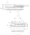
図1は、本発明に係るベース基板の部分拡大図であり、図2は、図1に対する本発明の一実施例によるタッチセンサモジュールのA−A部分の結合断面図であり、図3は、図1に対する本発明の一実施例によるタッチセンサモジュールのB−B部分の結合断面図であり、図4は、本発明の第2実施例によるタッチセンサモジュールの断面図であり、図5は、図4に対する電極パターンの平面図であり、図6から図8は、本発明の一実施例によるタッチセンサモジュールの製造方法の例示図である。 FIG. 1 is a partial enlarged view of a base substrate according to the present invention, FIG. 2 is a cross-sectional view of a touch sensor module according to an embodiment of the present invention with respect to FIG. 1 is a cross-sectional view of a touch sensor module according to an embodiment of the present invention with respect to FIG. 1, and FIG. 4 is a cross-sectional view of a touch sensor module according to a second embodiment of the present invention. FIG. 6 is a plan view of an electrode pattern with respect to FIG. 4, and FIGS.
本明細書の全体にわたり用いられている「タッチ」という用語は、接触受容面に対する直接の接触を意味するだけでなく、接触受容面に入力手段が相当近接していることも含む広い意味で解釈されるべきである。 As used throughout this specification, the term “touch” is interpreted in a broad sense that not only means direct contact with the contact-receiving surface, but also that the input means is in close proximity to the contact-receiving surface. It should be.
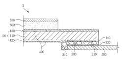
本発明の一実施例によるタッチセンサモジュール1は、電極パターン120、130、および前記電極パターン120、130の電気的信号を外部に伝達する電極パッド140を具備するベース基板110と、前記電極パターン120、130の表面に塗布されるパッシベーション層400と、前記電極パッド140の一面上に接して前記電気的信号を伝達するように形成された接着層200を具備するフレキシブルケーブル300と、を含み、前記パッシベーション層400が電極パッド140に重ならないように形成される。
The
本発明の一実施例によるタッチセンサモジュール1は、耐湿性をはじめ耐環境性の特性をより向上させるためのものであって、タッチセンサモジュール1の内部への水分などの浸透を最小化するためのものである。これにより、高温多湿の環境でもその作動信頼性を維持することができ、ユーザの便宜を図り、タッチセンサモジュール1の適用製品の分野をより多様化することができる。
A
本発明において、タッチセンサ100としては、抵抗膜方式または静電容量方式、その他の様々なタッチセンサ100が適用されてもよく、タッチセンサ100の形態および種類は特に限定されない。ただし、本発明の一実施例によるタッチセンサモジュール1では、ベース基板110の両面に電極パターン120、130が形成された静電容量方式のタッチセンサ100を一つの例として説明する。
In the present invention, as the
図1から図3を参照して説明すると、ベース基板110は、電極パターン120、130および電極配線150、160が形成される領域を提供する機能を果たす。ここで、ベース基板110は、アクティブ領域とベゼル領域とに分けられ、アクティブ領域は入力手段のタッチを認識するように電極パターン120、130が形成される部分としてベース基板110の中心に設けられ、ベゼル領域は電極パターン120、130から延長する電極配線150、160が形成される部分としてアクティブ領域の周縁に設けられる(図1を参照)。この際、ベース基板110は、電極パターン120、130および電極配線150、160を支持するための支持力と、画像表示装置(図示せず)で提供する画像をユーザに認識させるための透明性を備えなければならない。
Referring to FIGS. 1 to 3, the
上述の支持力および透明性を考慮すると、ベース基板110の材質は、ポリエチレンテレフタレート(PET)、ポリカーボネート(PC)、ポリメチルメタクリレート(PMMA)、ポリエチレンナフタレート(PEN)、ポリエーテルスルフォン(PES)、環状オレフィンコポリマー(COC)、トリアセチルセルロース(Triacetylcellulose;TAC)フィルム、ポリビニルアルコール(Polyvinyl alcohol;PVA)フィルム、ポリイミド(Polyimide;PI)フィルム、ポリスチレン(Polystyrene;PS)、二軸延伸ポリスチレン(K樹脂含有biaxially oriented PS;BOPS)、ガラスまたは強化ガラスなどからなることが好ましいが、必ずしもこれに限定されるものではない。ベース基板110の一面には後述する第1電極パターン120が形成され、他面には第2電極パターン130が形成される。
Considering the above-mentioned supporting force and transparency, the material of the
電極パターン120、130は、入力手段がタッチする際に信号を発生してコントローラでタッチ座標を認識させる機能を果たすものであり、ベース基板110に形成される。本発明の実施例では、ベース基板110のX軸方向に形成される電極パターンを第1電極パターン120とし、ベース基板110のY軸方向に形成される電極パターンを第2電極パターン130とする。
The
電極パターン120、130は、メッキ工程またはスパッタ(Sputter)を用いる蒸着工程で形成することができる。電極パターン120、130は、銀塩乳剤層を露光/現像して形成された金属を使用してもよく、導電性を有する金属でメッシュパターンを形成できる各種の物質を選択してもよいことは当業者にとって自明である。電極パターン120、130は、菱形パターン、四角形パターン、三角形パターン、円形パターンなど、当業界に公知のいずれのパターンに形成されてもよい。
The
電極配線150、160は、上述の電極パターン120、130とフレキシブルケーブル300を電気的信号で連結する。電極配線150、160は、シルクスクリーン法、グラビア印刷法またはインクジェット印刷法など、様々な印刷法でベース基板110上に形成することができる(図3を参照)。
The
電極配線150、160の素材としては、銅(Cu)、アルミニウム(Al)、金(Au)、銀(AG)、チタン(Ti)、パラジウム(Pd)、クロム(Cr)の材質を用いることができる。電極配線150、160には、電気伝導度に優れた銀ペースト(AG paste)または有機銀が用いられてもよい。ただし、このような例に限定されず、導電性高分子、カーボンブラック(CNTを含む)、ITOのような金属酸化物または金属類など、低抵抗の金属素材からなってもよい。
As materials for the
タッチセンサモジュール1の方式にしたがって、第1電極パターン120の一端にのみ電極配線150、160が連結される。電極配線150、160の末端部には、フレキシブルケーブル300と電気的に連結される電極パッド140が配置される。換言すれば、電極配線150、160の一部として電極パッド140が形成され、フレキシブルケーブル300が電気的に連結される。
According to the method of the
電極パッド140は、電極配線150、160に連結されてベース基板110に形成される(図1を参照)。電極パッド140は、フレキシブルケーブル300とベース基板110のアクティブ領域、すなわち、ユーザのタッチを認識する領域に踏み込まないように形成される。電極パッド140は、ベース基板110の一側先端部に配置されて電極配線150、160と連結される。
The
電極パッド140は、接着層200と接してフレキシブルケーブル300に電気を通すように形成される。電極パッド140は、フレキシブルケーブル300が加圧されることで接着層200と結合される。この際、電極パッド140には、ベース基板110の積層方向に接着層200が結合する。
The
電極パッド140には、接着層200の導電性ボール210と接する接触面が形成される。接触面は、導電性ボール210の直径より大きく形成される。電極パッド140は、ベース基板110の一側先端部に多数個が配置されてなる。この際、電極パッド140は、隣接した電極パッド同士が電気的干渉を起こさない距離だけ所定距離、離隔して形成される。
A contact surface that contacts the
本発明によれば、タッチセンサモジュール1の耐湿性をはじめ耐環境性の特性をより向上させることができる。パッシベーション層400がフレキシブルケーブル300および電極パッド140に互いに重ならないように形成されることで、導電性ボール210の浮き上がり現象および水分浸透を防止することができる。
According to the present invention, it is possible to further improve the environmental resistance characteristics including the moisture resistance of the
パッシベーション層400は、電極パターン120、130の表面を塗布することで形成される。パッシベーション層400は、電極パッド140の一側先端部まで形成される。すなわち、パッシベーション層400は、フレキシブルケーブル300と重ならないように形成される。パッシベーション層400は、電極パターン120、130、電極配線150、160および電極パッド140に水分が浸透することを防止する。
The
パッシベーション層400は、二酸化ケイ素(SiO2)または窒化ケイ素(SiN)からなる絶縁膜またはこれらを含む複合構造になるか、またはポリイミド、エポキシなどの素材からなってもよい。パッシベーション層400は、電極パッド140に重ならないように形成される。パッシベーション層400は、ベース基板110の電極パターン120、130が形成された一面または両面に形成される。パッシベーション層400は、電極パターン120、130の活性面を保護し、且つ水分浸透を防止する。パッシベーション層400は、後述するPI部310に導電性ボール210が所定圧力以上に加圧されると移動を遮断する係止段部の機能を果たす。
The
塗布層500は、パッシベーション層400または電極パターン120、130の表面に形成される。塗布層500は、パッシベーション層400と画像表示装置520を接着する。すなわち、塗布層500の一面にはパッシベーション層400が接着され、他面には画像表示装置520が接着される。これは、一例として、塗布層500がパッシベーション層400と画像表示装置520を接着する。これにより、塗布層500は、互いに異なる材質および装置を互いに接着して使用する。塗布層500の材質は、特に制限されず、光学透明接着剤(Optical Clear Adhesive、OCA)または両面接着テープ(Double Adhesive Tape、DAT)を用いてもよい。
The
フレキシブルケーブル300は、電極パッド140に対応して結合される。フレキシブルケーブル300は、接着層200と、端子部320とを含む。フレキシブルケーブル300は、電極パッド140に電気的に連結されて電極パターン120、130と制御部(図示せず)とを電気的に連結する。端子部320は、導電性ボール210と接して電気的に連結される。端子部320は、多数個の電極パッド140と対応する位置に形成される。端子部320は、電極パッド140に接着層200を加圧して接着される。
The
接着層200の下端面は電極パッド140に連結され、接着層200の上端面は端子部320に結合して接着される。すなわち、接着層200の内部に存在する導電性ボール210の一面は電極パッド140に接着され、他面は端子部320、330に接着される。これは、接着層200が電極パッド140と端子部320に接着される形態を限定するためではない。
The lower end surface of the
接着層200は、異方性導電フィルム(Anisotropic Conductive Film;ACF)からなることが好ましい。場合に応じて、異方性導電接着剤(Anisotropic Conductive Adhesive;ACA)などの導電性素材からなってもよい。
The
接着層200は、電極パッド140に接触して電気的に連結される。接着層200は、加圧により電極パッド140に結合されるか、加圧により接着される場合、導電性を有する導電性ボール210が内部に設けられる。導電性ボール210は、電極パッド140と端子部320が結合過程中に加圧により接合されて、一方向に電気を通す。この際、接着層200は、加圧により、接着液の一部がパッシベーション層400の方向に流出する。すなわち、加圧により、導電性ボール210の一部がPI部310に移動する。
The
PI部310は、パッシベーション層400とフレキシブルケーブル300が重ならないようにする。PI部310は、フレキシブルケーブル300に一体に形成されて、電極パターン120、130の方向に突出する(図2および図3を参照)。
The
PI部310は、外部の衝撃および湿気から導電性ボール210を保護し、且つ導電性ボール210の加圧状態を調節する。PI部310の厚さを調節して導電性ボール210の加圧状態を調節することができる。
The
PI部310は、パッシベーション層400と電極パッド140の段差による導電性ボール210の浮き上がり現象を防止する。PI部310の材質としてはフレキシブルケーブル300と同じ材質を用いてもよい。
The
PI部310は、電極パッド140とフレキシブルケーブル300との接着の際に段差が生じないようにする。すなわち、フレキシブルケーブル300と電極パッド140との間で導電性ボール210が所定の圧力を受けるようにする。すなわち、PI部310は、フレキシブルケーブル300と電極パッド140が接着層200に均等な圧力を印加するようにする。
The
PI部310は、電極パターン120、130、電極パッド140およびフレキシブルケーブル300が電気的に連結されるようにする。すなわち、PI部310は、電気的通電に対する不良を改善して製品の信頼性を確保する。
The
PI部310の突出長さは、導電性ボール210の直径より長い(図2および図3を参照)。PI部310は、電極パターン120、130と電極パッド140が加圧の際にショートしないようにする。PI部310は、フレキシブルケーブル300と電極パッド140の組立工程の際に発生する組立公差を最小化する。PI部310の突出長さは、導電性ボール210の組立公差と、導電性ボール210の直径を考慮して、500μm以上に形成されることが好適である。
The protruding length of the
図4および図5を参照して説明すると、本発明の第2実施例によるタッチセンサモジュール1については、本発明に係る一実施例の同一構成要素であるベース基板110、接着層200、フレキシブルケーブル300、パッシベーション層400およびフレキシブルケーブル300の構造および材質に関する説明は省略し、本発明に係る第2実施例の電極パターン120、130について詳細に説明する。
Referring to FIGS. 4 and 5, for the
ベース基板110の一面上に電極パターン120、130が形成されることで、単層の電極パターン120、130でタッチセンサが形成される。
By forming the
本発明に係る第1変形例のタッチセンサモジュールは、ベース基板110上に、X軸方向の第1電極パターン120と、第1電極パターン120に交差するY軸方向の第2電極パターン130を形成することができる(図5を参照)。
In the touch sensor module according to the first modification of the present invention, the
片面に第1電極パターン120と第2電極パターン130が交差して形成されるために、第1電極パターン120と第2電極パターン130が交差する部分には、いずれか一つの電極パターン上に絶縁パターンIが形成され、絶縁パターンI上に他の電極パターンが電気的に連結されるようにすることで、交差する第1電極パターン120と第2電極パターン130を電気的に連結することができる。交差する第1電極パターン120と第2電極パターン130の交差角は垂直のものに示されているが、その交差角に特に限定されず、二次元平面での座標を抽出するために、X軸とY軸の座標が出るように好適な角度に交差することが好ましい。電極パターン120、130の形成方法および材質については、上述の一実施例の電極パターンと同一であるため省略する。
Since the
図6および図8を参照して説明すると、本発明の一実施例によるタッチセンサモジュールの製造方法については、本発明に係る一実施例の同一構成要素であるベース基板110、接着層200、フレキシブルケーブル300、パッシベーション層400およびフレキシブルケーブル300の構造および材質に関する説明は省略する。
Referring to FIGS. 6 and 8, a method for manufacturing a touch sensor module according to an embodiment of the present invention includes a
本発明の一実施例によるタッチセンサモジュールの製造方法は、a)電極パターンおよび電極パッドが形成されたベース基板を準備する段階と、b)前記電極パターンおよび前記電極パッドの一側先端部まで塗布するパッシベーション層を形成する段階と、c)前記電極パッドに、接着層を用いてフレキシブルケーブルを連結する段階と、を含む。 A method of manufacturing a touch sensor module according to an embodiment of the present invention includes: a) preparing a base substrate on which an electrode pattern and an electrode pad are formed; and b) applying to one end of the electrode pattern and the electrode pad. Forming a passivation layer, and c) connecting a flexible cable to the electrode pad using an adhesive layer.
a)段階において、電極パターンおよび電極パッドが形成されたベース基板を準備する。図6を参照して説明すると、電極パターンの表面にパッシベーション層400を形成する。この際、パッシベーション層400を電極パッドの一側先端部まで塗布する。すなわち、パッシベーション層400がフレキシブルケーブルと重ならないようにする。
In step a), a base substrate on which an electrode pattern and an electrode pad are formed is prepared. Referring to FIG. 6, a
図7を参照して説明すると、b)段階において、パッシベーション層400の表面に塗布層500を形成する。塗布層500の一面にはパッシベーション層400を接着し、他面には画像表示装置520を接着する。塗布層500は、光学透明接着剤(Optical Clear Adhesive、OCA)または両面接着テープ(Double Adhesive Tape、DAT)を用いて、画像表示装置520をパッシベーション層400に接着する(図7を参照)。
Referring to FIG. 7, the
図8を参照して説明すると、c)段階は、電極パッド140に、接着層200を用いてフレキシブルケーブル300を連結する段階である。電極パッド140に接着層200を接着する。この際、接着層200が電極パッド140に密着して接着するように加圧する。接着層200は、加圧により、接着液が電極パターン120、130に流出する。すなわち、接着層200の導電性ボール210がパッシベーション層400に流れる。
Referring to FIG. 8, step c) is a step of connecting the
PI部310の方向に導電性ボールが移動するか、PI部310に予め配置された導電性ボール210がパッシベーション層400に重なる。PI部310で加圧される導電性ボール210が硬化されて湿気を防止する。また、PI部310に配置された導電性ボール210は、電極パッド140と端子部320との間に配置される導電性ボール210よりあまり加圧されない。PI部310の厚さおよび長さは、導電性ボール210の押圧状態および組立公差と密接な関係がある。
The conductive ball moves in the direction of the
例えば、PI部310の厚さがフレキシブルケーブル300の厚さより厚い場合には、電極パッド140と端子部320との間に配置される導電性ボール210が電気的にショートする。すなわち、電極パッド140と端子部320との間の導電性ボール210には浮き上がり現象が発生する。
For example, when the
また、PI部310の長さが導電性ボール210の直径より短い場合には、組立公差により、電極パッド140と端子部320との間に配置される導電性ボール210に組立不良が生じて電気ショートが発生する。さらに、導電性ボール210が電極パターン120、130の方向に移動してショートが発生する。そのため、PI部310の突出長さは、導電性ボール210の組立公差と、導電性ボール210の直径を考慮して500μm以上に形成されることが好適である。
In addition, when the length of the
以上、本発明を具体的な実施例に基づいて詳細に説明したが、これは本発明を具体的に説明するためのものであり、本発明はこれに限定されず、該当分野における通常の知識を有する者であれば、本発明の技術的思想内にての変形や改良が可能であることは明白であろう。 As described above, the present invention has been described in detail based on the specific embodiments. However, the present invention is only for explaining the present invention, and the present invention is not limited thereto. It will be apparent to those skilled in the art that modifications and improvements within the technical idea of the present invention are possible.
本発明の単純な変形乃至変更はいずれも本発明の領域に属するものであり、本発明の具体的な保護範囲は添付の特許請求の範囲により明確になるであろう。 All simple variations and modifications of the present invention belong to the scope of the present invention, and the specific scope of protection of the present invention will be apparent from the appended claims.
本発明は、タッチセンサモジュールおよびその製造方法に適用可能である。 The present invention is applicable to a touch sensor module and a manufacturing method thereof.
1 タッチセンサモジュール
100 タッチセンサ
110 ベース基板
120 第1電極パターン(電極パターン)
130 第2電極パターン(電極パターン)
140 電極パッド
150 第1電極配線(電極配線)
160 第2電極配線(電極配線)
200 接着層
210 導電性ボール
300 フレキシブルケーブル
310 PI部
320 第1端子部(端子部)
330 第2端子部(端子部)
400 パッシベーション層
500 塗布層
520 画像表示装置
DESCRIPTION OF
130 Second electrode pattern (electrode pattern)
140
160 Second electrode wiring (electrode wiring)
200
330 2nd terminal part (terminal part)
400
Claims (14)
前記電極パターンの表面に塗布されるパッシベーション層と、
前記電極パッドに対応して形成された端子部、および前記電極パッドと前記端子部との間に配置される接着層を具備するフレキシブルケーブルと、を含み、
前記パッシベーション層が、前記端子部に重ならないように形成されている、タッチセンサモジュール。 A base substrate comprising an electrode pattern and an electrode pad for transmitting an electrical signal of the electrode pattern to the outside;
A passivation layer applied to the surface of the electrode pattern;
Including a terminal portion formed corresponding to the electrode pad, and a flexible cable including an adhesive layer disposed between the electrode pad and the terminal portion,
The touch sensor module, wherein the passivation layer is formed so as not to overlap the terminal portion.
b)前記電極パターンおよび前記電極パッドの一側先端部まで塗布するパッシベーション層を形成する段階と、
c)前記電極パッドに、接着層を用いてフレキシブルケーブルを連結する段階と、を含む、タッチセンサモジュールの製造方法。 a) preparing a base substrate on which an electrode pattern and an electrode pad are formed;
b) forming a passivation layer to be applied up to one end of the electrode pattern and the electrode pad;
and c) connecting a flexible cable to the electrode pad using an adhesive layer.
前記フレキシブルケーブルの一側方向に突出して、湿気を防止し、且つ接着層が剥離することを防止するPI部を形成する、請求項9に記載のタッチセンサモジュールの製造方法。 c) In step
The touch sensor module manufacturing method according to claim 9, wherein a PI portion that protrudes in one direction of the flexible cable is formed to prevent moisture and prevent the adhesive layer from peeling off.
Applications Claiming Priority (2)
| Application Number | Priority Date | Filing Date | Title |
|---|---|---|---|
| KR10-2013-0142875 | 2013-11-22 | ||
| KR1020130142875A KR20150059375A (en) | 2013-11-22 | 2013-11-22 | Touch sensor module and manufacturing method thereof |
Publications (1)
| Publication Number | Publication Date |
|---|---|
| JP2015103244A true JP2015103244A (en) | 2015-06-04 |
Family
ID=53182230
Family Applications (1)
| Application Number | Title | Priority Date | Filing Date |
|---|---|---|---|
| JP2014195823A Pending JP2015103244A (en) | 2013-11-22 | 2014-09-25 | Touch sensor module and method for manufacturing the same |
Country Status (3)
| Country | Link |
|---|---|
| US (1) | US20150145791A1 (en) |
| JP (1) | JP2015103244A (en) |
| KR (1) | KR20150059375A (en) |
Families Citing this family (6)
| Publication number | Priority date | Publication date | Assignee | Title |
|---|---|---|---|---|
| KR20150033415A (en) * | 2013-09-24 | 2015-04-01 | 삼성전기주식회사 | Touch Sensor Module |
| KR102557962B1 (en) * | 2016-06-28 | 2023-07-24 | 삼성디스플레이 주식회사 | Flat panel display device having a touch screen and method of fabricating the same |
| KR102347961B1 (en) | 2016-10-28 | 2022-01-06 | 삼성디스플레이 주식회사 | Display device and manufacturing method thereof |
| CN106965534A (en) * | 2017-03-24 | 2017-07-21 | 信利光电股份有限公司 | A kind of preparation method of touch-control display module |
| KR102413716B1 (en) * | 2017-09-25 | 2022-06-28 | 삼성디스플레이 주식회사 | Display panel |
| CN110837309A (en) * | 2018-08-15 | 2020-02-25 | 宸美(厦门)光电有限公司 | Touch module and manufacturing method thereof |
Citations (1)
| Publication number | Priority date | Publication date | Assignee | Title |
|---|---|---|---|---|
| JP2015018317A (en) * | 2013-07-09 | 2015-01-29 | 日本写真印刷株式会社 | Touch sensor and manufacturing method of touch sensor |
Family Cites Families (6)
| Publication number | Priority date | Publication date | Assignee | Title |
|---|---|---|---|---|
| US7193218B2 (en) * | 2003-10-29 | 2007-03-20 | Canon Kabushiki Kaisha | Radiation detection device, method of producing the same, and radiation image pick-up system |
| JP4579074B2 (en) * | 2005-07-15 | 2010-11-10 | 三菱電機株式会社 | Flexible circuit board and display device using the same |
| KR101065409B1 (en) * | 2009-11-04 | 2011-09-16 | 삼성모바일디스플레이주식회사 | Organic light emitting diode lighting apparatus |
| CN102103428B (en) * | 2009-12-18 | 2013-01-02 | 群康科技(深圳)有限公司 | Flexible circuit board combining method of touch display device and touch display device |
| CN103094737A (en) * | 2011-11-05 | 2013-05-08 | 宝宸(厦门)光学科技有限公司 | Pin structure and pin connecting structure |
| KR102035005B1 (en) * | 2012-12-24 | 2019-10-22 | 엘지디스플레이 주식회사 | Touch display device |
-
2013
- 2013-11-22 KR KR1020130142875A patent/KR20150059375A/en not_active Application Discontinuation
-
2014
- 2014-09-25 JP JP2014195823A patent/JP2015103244A/en active Pending
- 2014-10-03 US US14/506,068 patent/US20150145791A1/en not_active Abandoned
Patent Citations (1)
| Publication number | Priority date | Publication date | Assignee | Title |
|---|---|---|---|---|
| JP2015018317A (en) * | 2013-07-09 | 2015-01-29 | 日本写真印刷株式会社 | Touch sensor and manufacturing method of touch sensor |
Also Published As
| Publication number | Publication date |
|---|---|
| KR20150059375A (en) | 2015-06-01 |
| US20150145791A1 (en) | 2015-05-28 |
Similar Documents
| Publication | Publication Date | Title |
|---|---|---|
| US20130161177A1 (en) | Touch panel | |
| US8956181B2 (en) | Connection structure between substrate and FPCB for touch panel | |
| JP2015103244A (en) | Touch sensor module and method for manufacturing the same | |
| US8466891B2 (en) | Touch panel | |
| US20130277094A1 (en) | Touch panel and method for manufacturing the same | |
| JP2013025783A (en) | Touch panel | |
| JP2011210224A (en) | Touch panel | |
| US20120032910A1 (en) | Touch panel and method of manufacturing the same | |
| JP2014021962A (en) | Touch panel and method for manufacturing the same | |
| JP2014044716A (en) | Flexible circuit board and touch panel including the same | |
| JP2015153422A (en) | Touch sensor and method of manufacturing the same | |
| US20150082897A1 (en) | Touch sensor module | |
| JP2015018532A (en) | Touch sensor | |
| US20120001863A1 (en) | Touch panel | |
| JP2011175612A (en) | Touch panel | |
| JP2015191662A (en) | touch sensor module | |
| US20120019486A1 (en) | Touch panel and method of manufacturing the same | |
| JP2012064188A (en) | Capacitive touch panel and its manufacturing method | |
| TWM488681U (en) | Touch panel | |
| JP2015103242A (en) | Touch sensor module and method for manufacturing the same | |
| JP2014120149A (en) | Touch panel | |
| JP2013134766A (en) | Joint structure for touch panel and method for manufacturing the same | |
| JP2012064211A (en) | Manufacturing method for electrostatic capacitive touch screen | |
| JP2015090704A (en) | Touch sensor module | |
| JP2015036974A (en) | Touch sensor module |
Legal Events
| Date | Code | Title | Description |
|---|---|---|---|
| A977 | Report on retrieval |
Free format text: JAPANESE INTERMEDIATE CODE: A971007 Effective date: 20151014 |
|
| A131 | Notification of reasons for refusal |
Free format text: JAPANESE INTERMEDIATE CODE: A131 Effective date: 20151020 |
|
| A02 | Decision of refusal |
Free format text: JAPANESE INTERMEDIATE CODE: A02 Effective date: 20160315 |