JP2015018532A - Touch sensor - Google Patents
Touch sensor Download PDFInfo
- Publication number
- JP2015018532A JP2015018532A JP2013220366A JP2013220366A JP2015018532A JP 2015018532 A JP2015018532 A JP 2015018532A JP 2013220366 A JP2013220366 A JP 2013220366A JP 2013220366 A JP2013220366 A JP 2013220366A JP 2015018532 A JP2015018532 A JP 2015018532A
- Authority
- JP
- Japan
- Prior art keywords
- insulating layer
- bezel
- height
- touch sensor
- window substrate
- Prior art date
- Legal status (The legal status is an assumption and is not a legal conclusion. Google has not performed a legal analysis and makes no representation as to the accuracy of the status listed.)
- Pending
Links
Images


Classifications
-
- G—PHYSICS
- G06—COMPUTING; CALCULATING OR COUNTING
- G06F—ELECTRIC DIGITAL DATA PROCESSING
- G06F3/00—Input arrangements for transferring data to be processed into a form capable of being handled by the computer; Output arrangements for transferring data from processing unit to output unit, e.g. interface arrangements
- G06F3/01—Input arrangements or combined input and output arrangements for interaction between user and computer
- G06F3/03—Arrangements for converting the position or the displacement of a member into a coded form
- G06F3/041—Digitisers, e.g. for touch screens or touch pads, characterised by the transducing means
- G06F3/044—Digitisers, e.g. for touch screens or touch pads, characterised by the transducing means by capacitive means
- G06F3/0446—Digitisers, e.g. for touch screens or touch pads, characterised by the transducing means by capacitive means using a grid-like structure of electrodes in at least two directions, e.g. using row and column electrodes
-
- G—PHYSICS
- G06—COMPUTING; CALCULATING OR COUNTING
- G06F—ELECTRIC DIGITAL DATA PROCESSING
- G06F3/00—Input arrangements for transferring data to be processed into a form capable of being handled by the computer; Output arrangements for transferring data from processing unit to output unit, e.g. interface arrangements
- G06F3/01—Input arrangements or combined input and output arrangements for interaction between user and computer
- G06F3/03—Arrangements for converting the position or the displacement of a member into a coded form
- G06F3/041—Digitisers, e.g. for touch screens or touch pads, characterised by the transducing means
- G06F3/0416—Control or interface arrangements specially adapted for digitisers
-
- G—PHYSICS
- G06—COMPUTING; CALCULATING OR COUNTING
- G06F—ELECTRIC DIGITAL DATA PROCESSING
- G06F3/00—Input arrangements for transferring data to be processed into a form capable of being handled by the computer; Output arrangements for transferring data from processing unit to output unit, e.g. interface arrangements
- G06F3/01—Input arrangements or combined input and output arrangements for interaction between user and computer
- G06F3/03—Arrangements for converting the position or the displacement of a member into a coded form
- G06F3/041—Digitisers, e.g. for touch screens or touch pads, characterised by the transducing means
- G06F3/044—Digitisers, e.g. for touch screens or touch pads, characterised by the transducing means by capacitive means
- G06F3/0445—Digitisers, e.g. for touch screens or touch pads, characterised by the transducing means by capacitive means using two or more layers of sensing electrodes, e.g. using two layers of electrodes separated by a dielectric layer
-
- H—ELECTRICITY
- H05—ELECTRIC TECHNIQUES NOT OTHERWISE PROVIDED FOR
- H05K—PRINTED CIRCUITS; CASINGS OR CONSTRUCTIONAL DETAILS OF ELECTRIC APPARATUS; MANUFACTURE OF ASSEMBLAGES OF ELECTRICAL COMPONENTS
- H05K3/00—Apparatus or processes for manufacturing printed circuits
- H05K3/10—Apparatus or processes for manufacturing printed circuits in which conductive material is applied to the insulating support in such a manner as to form the desired conductive pattern
-
- G—PHYSICS
- G06—COMPUTING; CALCULATING OR COUNTING
- G06F—ELECTRIC DIGITAL DATA PROCESSING
- G06F2203/00—Indexing scheme relating to G06F3/00 - G06F3/048
- G06F2203/041—Indexing scheme relating to G06F3/041 - G06F3/045
- G06F2203/04103—Manufacturing, i.e. details related to manufacturing processes specially suited for touch sensitive devices
-
- Y—GENERAL TAGGING OF NEW TECHNOLOGICAL DEVELOPMENTS; GENERAL TAGGING OF CROSS-SECTIONAL TECHNOLOGIES SPANNING OVER SEVERAL SECTIONS OF THE IPC; TECHNICAL SUBJECTS COVERED BY FORMER USPC CROSS-REFERENCE ART COLLECTIONS [XRACs] AND DIGESTS
- Y10—TECHNICAL SUBJECTS COVERED BY FORMER USPC
- Y10T—TECHNICAL SUBJECTS COVERED BY FORMER US CLASSIFICATION
- Y10T29/00—Metal working
- Y10T29/49—Method of mechanical manufacture
- Y10T29/49002—Electrical device making
- Y10T29/49117—Conductor or circuit manufacturing
- Y10T29/49124—On flat or curved insulated base, e.g., printed circuit, etc.
- Y10T29/49155—Manufacturing circuit on or in base
Abstract
Description
本発明は、タッチセンサに関する。 The present invention relates to a touch sensor.
デジタル技術を用いるコンピュータが発達するにつれて、コンピュータの補助装置もともに開発されており、パソコン、携帯用送信装置、その他の個人用の情報処理装置などは、キーボード、マウスなどの様々な入力装置(Input Device)を利用してテキストおよびグラフィック処理を行う。 Along with the development of computers using digital technology, computer auxiliary devices have been developed. Personal computers, portable transmission devices, and other personal information processing devices have various input devices such as keyboards and mice (Inputs). Text and graphics processing is performed using Device).
しかし、情報化社会の急速な進行により、コンピュータの用途が益々拡大する傾向にあるため、現在、入力装置の役割を担当しているキーボードおよびマウスだけでは、効率的な製品の駆動が困難であるという問題点がある。従って、簡単で誤操作が少なく、誰でも簡単に情報を入力することができる機器の必要性が高まっている。 However, due to the rapid progress of the information society, the use of computers tends to expand more and more, so it is difficult to drive products efficiently with only the keyboard and mouse that are currently in charge of input devices. There is a problem. Accordingly, there is an increasing need for a device that is simple and has few erroneous operations and that allows anyone to easily input information.
また、入力装置に関する技術は、一般的な機能を満たす水準を超えて、高信頼性、耐久性、革新性、設計および加工に関する技術などが注目されており、このような目的を達成するために、テキスト、グラフィックなどの情報入力が可能な入力装置としてタッチセンサ(touch sensor)が開発された。 In addition, the technology related to input devices has exceeded the level that satisfies general functions, and attention has been paid to technologies related to high reliability, durability, innovation, design and processing, etc. In addition, a touch sensor has been developed as an input device capable of inputting information such as text and graphics.
タッチセンサは、電子手帳、液晶表示装置(LCD;Liquid Crystal Display Device)、PDP(Plasma Display Panel)、El(Electroluminescence)などの平板ディスプレイ装置およびCRT(Cathode Ray Tube)などの画像表示装置の表示面に設けられ、ユーザが画像表示装置を見ながら所望の情報を選択するようにするために利用される機器である。 The touch sensor is a display device such as an electronic notebook, a liquid crystal display device (LCD), a flat panel display device such as PDP (Plasma Display Panel), El (Electroluminescence), and a CRT (Cathode Ray Tube) display device. The device is used for the user to select desired information while looking at the image display device.
一方、タッチセンサの種類は、抵抗膜方式(Resistive Type)、静電容量方式(Capacitive Type)、電磁方式(Electro−Magnetic Type)、表面弾性波方式(SAW Type;Surface Acoustic Wave Type)および赤外線方式(Infrared Type)に区分される。このような様々な方式のタッチセンサは、信号増幅の問題、解像度の差、設計および加工技術の難易度、光学的特性、電気的特性、機械的特性、耐環境特性、入力特性、耐久性および経済性を考慮して電子製品に採用されるが、現在もっとも幅広い分野で用いられている方式は、抵抗膜方式タッチセンサおよび静電容量方式タッチセンサである。 On the other hand, the types of touch sensors are a resistive film type, a capacitive type, an electromagnetic type (Electro-Magnetic Type), a surface acoustic wave type (SAW Type; Surface Acoustic Wave type), and an infrared type. (Infrared Type). Such various types of touch sensors have signal amplification problems, resolution differences, difficulty of design and processing technology, optical characteristics, electrical characteristics, mechanical characteristics, environmental resistance characteristics, input characteristics, durability and Although adopted for electronic products in consideration of economic efficiency, the methods used in the widest field at present are a resistive touch sensor and a capacitive touch sensor.
このようなタッチセンサには、通常、タッチセンサ構造の最外側に設けられるウィンドウガラス(window glass)に、電極配線を隠したり、装飾パターンが形成されえる黒色または白色などの色を有するベゼル部が形成される。 Such a touch sensor usually has a bezel portion having a color such as black or white that can hide an electrode wiring or form a decorative pattern on a window glass provided on the outermost side of the touch sensor structure. It is formed.
ベゼル部が形成されている従来のタッチセンサの具体的な一例としては、特許文献1に開示されたタッチセンサが挙げられる。
As a specific example of a conventional touch sensor in which a bezel portion is formed, a touch sensor disclosed in
しかし、従来のタッチセンサは、ベゼル部に電極を形成する際、ベゼル部の段差や表面の不均一性による電極の断線またはクラックが生じる問題がある。 However, the conventional touch sensor has a problem in that when the electrode is formed on the bezel portion, the electrode is disconnected or cracked due to the step of the bezel portion and the surface non-uniformity.
本発明は、上述の従来技術の問題点を解決するためのものであって、本発明の目的は、ベゼルによる段差や表面の不均一性を予め防止または減少させることで不良率を低減したタッチセンサを提供することにある。 The present invention is intended to solve the above-described problems of the prior art, and an object of the present invention is to reduce the defect rate by preventing or reducing the unevenness of the steps and the surface due to the bezel in advance. It is to provide a sensor.
本発明の一実施例によるベゼル組成物を含むタッチセンサは、ウィンドウ基板と、前記ウィンドウ基板の周縁に沿って形成されるベゼルと、前記ベゼルとベゼルとの間を充填しながら積層または接着されて、前記ウィンドウ基板上に形成される絶縁層と、前記絶縁層上に形成される電極パターンと、を含むタッチセンサを提供する。 A touch sensor including a bezel composition according to an exemplary embodiment of the present invention includes a window substrate, a bezel formed along a periphery of the window substrate, and a laminate or an adhesive while filling between the bezel and the bezel. A touch sensor including an insulating layer formed on the window substrate and an electrode pattern formed on the insulating layer is provided.
本発明の一実施例によるタッチセンサとして、前記絶縁層の材質として、アクリル(acryl)系、ウレタン(urethane)系、シリコーン(silicone)系、ポリエステル(polyester)系、ポリアミド(polyamide)系、エポキシ(epoxy)系、ビニルアルキルエーテル(vinyl alkyl ether)系、SiOxおよびSiNxなどの薄膜のうち一つを使用することが好適である。 In a touch sensor according to an embodiment of the present invention, the insulating layer may be made of acrylic, urethane, silicone, polyester, polyamide, epoxy (polyamide), epoxy (polyamide), epoxy (polyamide), epoxy (polyamide), epoxy (polyamide), It is preferable to use one of thin films such as epoxy, vinyl alkyl ether, SiOx and SiNx.
本発明の一実施例によるタッチセンサとして、ウィンドウ基板と、前記ウィンドウ基板の周縁に沿って形成されるベゼルと、前記ベゼルとベゼルとの間を充填しながら積層され、前記ウィンドウ基板上に形成される第1絶縁層と、前記ベゼルおよび第1絶縁層上に塗布および接着して形成される第2絶縁層と、前記第2絶縁層上に形成される電極パターンと、を含むタッチセンサを提供する。 As a touch sensor according to an embodiment of the present invention, a window substrate, a bezel formed along a periphery of the window substrate, and a stack between the bezel and the bezel are stacked and formed on the window substrate. There is provided a touch sensor including a first insulating layer, a second insulating layer formed by applying and adhering to the bezel and the first insulating layer, and an electrode pattern formed on the second insulating layer. To do.
本発明の一実施例によるタッチセンサとして、前記第1絶縁層は、前記ベゼルの高さ(BL)まで積層されてなることが好ましい。 As a touch sensor according to an embodiment of the present invention, the first insulating layer is preferably stacked up to the height (BL) of the bezel.
本発明の一実施例によるタッチセンサとして、積層方向における前記ベゼルの高さ(BL)は、次の式:0μm<高さ(BL)≦40μmを満たすことが好適である。 As a touch sensor according to an embodiment of the present invention, the height (BL) of the bezel in the stacking direction preferably satisfies the following formula: 0 μm <height (BL) ≦ 40 μm.
本発明の一実施例によるタッチセンサとして、積層方向における前記第1絶縁層の高さ(L)は、次の式:0μm≦前記第1絶縁層の高さ(L)μm<(前記ベゼルの高さ(BL)×1.3)μmを満たすことが好ましい。 As a touch sensor according to an embodiment of the present invention, the height (L) of the first insulating layer in the stacking direction is expressed by the following formula: 0 μm ≦ the height of the first insulating layer (L) μm <(of the bezel It is preferable to satisfy height (BL) × 1.3) μm.
本発明の一実施例によるタッチセンサとして、前記ウィンドウ基板の中央点における高さ(d)は、次の式:積層方向における第2絶縁層の高さ(2L)×0.05μm<中央点における高さ(d)μm<前記第2絶縁層の高さ(2L)×1.3μmを満たすことが好適である。 As a touch sensor according to an embodiment of the present invention, the height (d) at the center point of the window substrate is expressed by the following formula: height of the second insulating layer in the stacking direction (2L) × 0.05 μm <at the center point. It is preferable that the height (d) μm <the height of the second insulating layer (2L) × 1.3 μm.
本発明の一実施例によるタッチセンサとして、積層方向における前記第2絶縁層の高さ(2L)は、ベゼルの高さ(BL)の3倍を超えないように形成されることが好ましい。 As a touch sensor according to an embodiment of the present invention, the height (2L) of the second insulating layer in the stacking direction is preferably formed so as not to exceed three times the height (BL) of the bezel.
本発明の一実施例によるタッチセンサとして、前記第1絶縁層と前記第2絶縁層の材質は同じ材質であることが好適である。 In the touch sensor according to the embodiment of the present invention, it is preferable that the first insulating layer and the second insulating layer are made of the same material.
本発明の一実施例によるタッチセンサとして、前記第1絶縁層と前記第2絶縁層の材質として、アクリル(acryl)系、ウレタン(urethane)系、シリコーン(silicone)系、ポリエステル(polyester)系、ポリアミド(polyamide)系、エポキシ(epoxy)系、ビニルアルキルエーテル(vinyl alkyl ether)系、SiOxおよびSiNxなどの薄膜のうち一つを使用することが好ましい。 As a touch sensor according to an embodiment of the present invention, the materials of the first insulating layer and the second insulating layer may be acrylic, urethane, silicone, polyester, It is preferable to use one of thin films such as polyamide, epoxy, vinyl alkyl ether, SiOx and SiNx.
本発明の第2実施例によるタッチセンサの製造方法として、a)周縁に沿ってベゼルが形成されたウィンドウ基板を固定する段階と、b)前記ウィンドウ基板の一面に形成され、且つ前記ベゼルとベゼルとの間に第1絶縁層を充填する段階と、c)前記ベゼルと第1絶縁層を横切って第2絶縁層を形成する段階と、d)前記第2絶縁層上に電極パターンを形成する段階と、を含むタッチセンサの製造方法を提供する。 A method of manufacturing a touch sensor according to a second embodiment of the present invention includes: a) fixing a window substrate having a bezel formed along a peripheral edge; and b) forming the bezel on the one side of the window substrate and the bezel and the bezel. Filling a first insulating layer between c), c) forming a second insulating layer across the bezel and the first insulating layer, and d) forming an electrode pattern on the second insulating layer. And a method for manufacturing a touch sensor.
本発明の第2実施例によるタッチセンサの製造方法として、前記b)段階において、積層方向に形成された前記第1絶縁層の高さ(L)は、次の式:0≦L<(前記ベゼルの高さ(BL)×1.3)μmを満たすことが好適である。 In the touch sensor manufacturing method according to the second embodiment of the present invention, in the step b), the height (L) of the first insulating layer formed in the stacking direction may be expressed by the following formula: 0 ≦ L <(above It is preferable to satisfy the bezel height (BL) × 1.3) μm.
本発明の第2実施例によるタッチセンサの製造方法として、前記c)段階において、前記ウィンドウ基板の中央点における高さ(d)は、次の式:(積層方向における前記第2絶縁層の高さ(2L)×0.05)<d<(前記絶縁層の高さ(2L)×1.3)μmを満たすことが好ましい。 In the touch sensor manufacturing method according to the second embodiment of the present invention, in the step c), the height (d) at the center point of the window substrate is expressed by the following formula: (the height of the second insulating layer in the stacking direction). (2L) × 0.05) <d <(height of the insulating layer (2L) × 1.3) μm is preferably satisfied.
本発明の第2実施例によるタッチセンサの製造方法として、前記c)段階において、積層方向における前記第2絶縁層の高さ(2L)は、前記ベゼルの高さ(BL)に対して3倍の大きさを超えないように形成されることが好適である。 In the touch sensor manufacturing method according to the second embodiment of the present invention, in the step c), the height (2L) of the second insulating layer in the stacking direction is three times the height (BL) of the bezel. It is preferable that the size is not exceeded.
本発明の第2実施例によるタッチセンサの製造方法として、前記c)段階において、前記第2絶縁層は前記第1絶縁層と同じ材質を使用することが好ましい。 In the touch sensor manufacturing method according to the second embodiment of the present invention, in the step c), the second insulating layer is preferably made of the same material as the first insulating layer.
本発明によれば、絶縁層を形成することで、塗布工程時に生じる段差や表面の不均一性を除去または減少させて不良率を低減する効果がある。 According to the present invention, by forming the insulating layer, there is an effect of reducing or reducing the defect rate by removing or reducing the level difference and surface non-uniformity generated during the coating process.
また、本発明によれば、絶縁層を形成することで、電極の断線と誤動作を防止する効果がある。 In addition, according to the present invention, by forming the insulating layer, there is an effect of preventing disconnection and malfunction of the electrode.
そして、本発明によれば、平坦な絶縁層を形成することで、絶縁層の表面に電極を容易に形成できる効果がある。 And according to this invention, there exists an effect which can form an electrode on the surface of an insulating layer easily by forming a flat insulating layer.
また、本発明によれば、絶縁層を形成することで、電極の電気的な通電が向上したタッチセンサを提供することができる。 Further, according to the present invention, it is possible to provide a touch sensor in which electrical conduction of electrodes is improved by forming an insulating layer.
更に、本発明によれば、絶縁層を形成することで、電極に対する信頼性が向上したタッチセンサを提供することができる。 Furthermore, according to the present invention, it is possible to provide a touch sensor with improved reliability for electrodes by forming an insulating layer.
本発明の目的、特定の長所および新規の特徴は、添付図面に係る以下の詳細な説明および好ましい実施例によってさらに明らかになるであろう。本明細書において、各図面の構成要素に参照番号を付け加えるに際し、同一の構成要素に限っては、たとえ異なる図面に示されても、できるだけ同一の番号を付けるようにしていることに留意しなければならない。また、「一面」、「他面」、「第1」、「第2」などの用語は、一つの構成要素を他の構成要素から区別するために用いられるものであり、構成要素が前記用語によって限定されるものではない。以下、本発明を説明するにあたり、本発明の要旨を不明瞭にする可能性がある係る公知技術についての詳細な説明は省略する。 Objects, specific advantages and novel features of the present invention will become more apparent from the following detailed description and preferred embodiments with reference to the accompanying drawings. In this specification, it should be noted that when adding reference numerals to the components of each drawing, the same components are given the same number as much as possible even if they are shown in different drawings. I must. The terms “one side”, “other side”, “first”, “second” and the like are used to distinguish one component from another component, and the component is the term It is not limited by. Hereinafter, in describing the present invention, detailed descriptions of known techniques that may obscure the subject matter of the present invention are omitted.
以下、添付図面を参照して、本発明の好ましい実施例を詳細に説明する。 Hereinafter, preferred embodiments of the present invention will be described in detail with reference to the accompanying drawings.
図1は、本発明の一実施例によるタッチセンサの平面図であり、図2は、図1に対するタッチセンサの断面図であり、図3は、第1絶縁層を含む図1のタッチセンサの断面図であり、図4は、図3の第2絶縁層が形成された断面図であり、図5は、スクリーン印刷方式の工程時に発生する形状の例示図であり、図6は、ドライフィルムラミネーション工程時の例示図であり、図7は、本発明の第2実施例によるタッチセンサの断面図であり、図8は、本発明の一実施例によるタッチセンサの製造工程を示す図である。 1 is a plan view of a touch sensor according to an embodiment of the present invention, FIG. 2 is a cross-sectional view of the touch sensor with respect to FIG. 1, and FIG. 3 is a cross-sectional view of the touch sensor of FIG. 4 is a cross-sectional view in which the second insulating layer of FIG. 3 is formed, FIG. 5 is an exemplary view of a shape generated during a screen printing process, and FIG. 6 is a dry film. FIG. 7 is a cross-sectional view of a touch sensor according to a second embodiment of the present invention, and FIG. 8 is a diagram illustrating a touch sensor manufacturing process according to an embodiment of the present invention. .
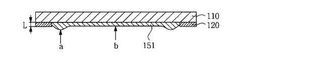
図1を参照して説明すると、本発明の一実施例によるタッチセンサは、ウィンドウ基板110と、ウィンドウ基板110の非活性領域に配置されるベゼル120と、を含む。
Referring to FIG. 1, a touch sensor according to an embodiment of the present invention includes a
本発明は、ウィンドウ基板110とベゼル120の加工時に生じる段差を除去するか最小化して、絶縁層150上に形成される電極パターン140の電気的な作動信頼性を向上させる。また、加工工程の収率を向上させることで、タッチセンサ1の生成率を向上させる。
The present invention removes or minimizes the level difference generated when the
図1および図2を参照して説明すると、ウィンドウ基板110は、タッチ位置を検出するための電極パターン140が形成される領域を提供する役割を行うことができる。ウィンドウ基板110は、電極パターン140を支持するための支持力、および画像表示装置で提供される画像をユーザが認識するための透明性を備えなければならない。ウィンドウ基板110に、第1絶縁層151と第2絶縁層152が順に塗布されて積層される。
Referring to FIGS. 1 and 2, the
ウィンドウ基板110は、タッチセンサ1の最外側でユーザのタッチが入力される方向に形成され、所定強度以上の強化ガラス等を使用することでタッチセンサ1を保護する保護層の役割を同時に行うことができる。上述の支持力および透明性を考慮すると、ウィンドウ基板110は、透明度を考慮して、ポリエチレンテレフタレート(PET)、ポリカーボネート(PC)、ポリメチルメタクリレート(PMMA)、ポリエチレンナフタレート(PEN)、ポリエーテルスルフォン(PES)、環状オレフィンコポリマー(COC)、トリアセチルセルロース(Triacetylcellulose;TAC)フィルム、ポリビニルアルコール(Polyvinyl alcohol;PVA)フィルム、ポリイミド(Polyimide;PI)フィルム、ポリスチレン(Polystyrene;PS)、二軸延伸ポリスチレン(K樹脂含有biaxially oriented PS;BOPS)などの材質を使用してもよい。
The
一方、ウィンドウ基板110は、図1に示されたように、活性領域111と、活性領域111の周縁に沿って形成される非活性領域112とに分けられる。活性領域111は、ユーザによるタッチ作用が行われる領域であり、ユーザが機器の動作場面を視覚的に確認する画面領域である。また、非活性領域112は、ウィンドウ基板110に形成される、後述するベゼル120で隠されて外部に露出しない領域である。
Meanwhile, the
ベゼル120は、ウィンドウ基板110の非活性領域112に形成される。ベゼル120は、ウィンドウ基板110の周縁に沿って配置される。すなわち、ベゼル120は、非活性領域112の一側に配置されて0μmから40μm以下の高さ(BL)を有するように形成されることが好ましい。タッチセンサ1の視認性および製品の厚さを考慮してベゼル120の高さ(BL)が決まる。
The
ベゼル120は、ウィンドウ基板110の非活性領域112で配線電極の一側を隠すか装飾の役割を行う。また、ベゼル120には、必要に応じて、製造社のロゴなどの装飾パターンが形成されてもよい。
The
図3および図4を参照して説明すると、絶縁層150は、後述する電極パターン140を保護する役割を行う。絶縁層150は、第1絶縁層151と第2絶縁層152が順に積層される。絶縁層150は、ベゼル120の高さ(BL)まで塗布して絶縁する第1絶縁層151と、第1絶縁層151の表面を塗布する第2絶縁層152と、を含む。場合に応じて、段差がある程度許容されるが、表面の不均一性を解消する必要がある場合は、第1絶縁層の塗布を省略してもよい。この場合、第1絶縁層の塗布を省略し、スピンコーティングやフィルム形態で第2絶縁層を接着または塗布することができる。この場合、絶縁層は、図6に示された形態と同様な形態を有する。
Referring to FIGS. 3 and 4, the insulating
第1絶縁層151は、ウィンドウ基板110の一側に接し、ベゼル120とベゼル120との間を充填する。この際、第1絶縁層151は、ベゼル120の高さ(BL)まで塗布して水平な面を形成することが好ましい。これは、第1絶縁層151の高さ(L)とベゼル120の高さ(BL)が互いに水平をなすようにする。
The first insulating
第1絶縁層151は、プリンティング(Printing)、CVD(Chemical Vaper Deposition)、スパッタリング(Sputtering)、スピンコーティング、スロットダイ、ラミネーションなどにより有機絶縁膜または無機絶縁膜からなる。この際、第1絶縁層151の高さ(L)は、ベゼル120の高さ(BL)と水平をなすように塗布および接着工程を行う。この際、ベゼル120の高さ(BL)と、第1絶縁層151の高さ(L)との間で工程公差が発生する。
The first insulating
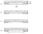
図5および図6を参照して、工程の一例として、スクリーンプリンティングとフィルムを使用する接着工程で生じる現象について説明する。第1絶縁層151の塗布液200または接着層が両側に偏る現象(図5の(a)参照)、第1絶縁層151の塗布液200または接着層がベゼル120の高さ(BL)より少なく投入される現象(図5の(b)、(c)参照)、第1絶縁層151の塗布液または接着層がベゼル120の高さ(BL)より多く投入される現象(図5の(d)参照)、第1絶縁層151の塗布液または接着層がベゼル120を横切ってベゼル120に接着される現象(図6を参照)などが生じる。このような現象は、ベゼル120とベゼル120との間に第1絶縁層151を充填させる工程で生じている。また、第1絶縁層151において上述の現象が生じる場合、配線電極または後述する電極パターン140上の電気的信号が短絡する問題点が生じた。また、電極パターン140を絶縁層150に水平に形成することが困難であるという問題点が発生した。
With reference to FIG. 5 and FIG. 6, as an example of a process, a phenomenon that occurs in an adhesion process using screen printing and a film will be described. Phenomenon in which the
図3を参照して説明すると、第1絶縁層151でベゼル120とベゼル120との間を充填する。この際、第1絶縁層151の高さ(L)は、次の式:0≦第1絶縁層151の高さ(L)≦ベゼル120の高さ(BL)×1.3μmを満たす。この際、ベゼル120の高さ(BL)は、次の式:0μm<ベゼルの高さ(BL)≦40μmを満たす。
Referring to FIG. 3, the space between the
第1絶縁層151の塗布液または接着層のa点とb点との高さの差が中央部分の高さに対して35%以下に形成される。第1絶縁層の加工公差は、(a点の高さ−b点の高さ)/b点の高さ×100<35%以内に形成される。すなわち、第1絶縁層151は、水平に形成されておらず、加工公差が存在することを確認できる。第1絶縁層151の材質として、アクリル(acryl)系、ウレタン(urethane)系、シリコーン(silicone)系、ポリエステル(polyester)系、ポリアミド(polyamide)系、エポキシ(epoxy)系、ビニルアルキルエーテル(vinyl alkyl ether)系、SiOxおよびSiNxなどの薄膜のうち一つを使用することが好ましい。
The difference in height between point a and point b of the coating liquid or adhesive layer of the first insulating
図4を参照して説明すると、第2絶縁層152は、第1絶縁層151とベゼル120の表面に形成される。第2絶縁層152は、第1絶縁層151とベゼル120の表面に接して形成される。第2絶縁層152は、ベゼル120の非活性領域112に形成された配線電極の断線を解消して電気的信頼性を向上させる。第2絶縁層152の中心dの高さは、第2絶縁層152の高さ(2L)×0.05μm<中心dの高さμm<第2絶縁層152の高さ(2L)×1.3μmを有する。すなわち、第2絶縁層152を塗布または接着すると、加工公差を著しく減少することを確認できる。
Referring to FIG. 4, the second insulating
第2絶縁層152の高さ(2L)は、2L(μm)/BL(μm)≦3を有することが好ましい。即ち、第1絶縁層151および第2絶縁層152と、ベゼル120の高さを含む高さは120μm以下に設定することが好ましい。
The height (2L) of the second insulating
第2絶縁層152の材質として、アクリル(acryl)系、ウレタン(urethane)系、シリコーン(silicone)系、ポリエステル(polyester)系、ポリアミド(polyamide)系、エポキシ(epoxy)系、ビニルアルキルエーテル(vinyl alkyl ether)系SiOxおよびSiNxなどの薄膜のうち一つを使用することが好ましい。これは、第2絶縁層152の材質を限定するためではない。第2絶縁層152は、第1絶縁層151と同じ材質で形成することが好ましい。
The material of the second insulating
電極パターン140は、第2絶縁層152上に形成される。1層構造の電極パターン140を用いて自己静電容量方式(Self Capacitive Type)タッチセンサまたは相互静電容量方式(Mutual Capacitive Type)タッチセンサを製作することができる。しかし、本発明に係るタッチセンサは、これに制限されるものではない。
The
本発明に係る第2実施例のタッチセンサについて説明するにあたり、第1実施例と同一の構成要素は省略し、本発明に係る第2実施例の電極パターンの構造について詳細に説明する。 In describing the touch sensor according to the second embodiment of the present invention, the same components as those of the first embodiment are omitted, and the structure of the electrode pattern of the second embodiment according to the present invention will be described in detail.
図7を参照して説明すると、電極パターン140は、第2絶縁層152上に形成される第1電極パターン141と、第1電極パターン141と離隔して形成される第2電極パターン142が形成される。電極パターン140は、第1電極パターン141と第2電極パターン142との間に接着層が形成される。接着層は、第1電極パターン141と第2電極パターン142が対向するように配置する役割を行う。ここで、第1接着層の材質は、特に制限されず、光学透明接着剤(Optical Clear Adhesive、OCA)、両面接着テープ(Double Adhesive Tape、DAT)またはその他の透明絶縁材料を用いてもよい。
Referring to FIG. 7, the
電極パターン140は、タッチの入力手段によって信号を発生させ、制御部(図示せず)からタッチ座標を認識するための役割を行うものである。第1電極パターン141と第2電極パターン142は、互いに交差する方向に形成されてもよい。例えば、第1電極パターン141がX軸方向に互いに平行に少なくとも一つ以上が形成される際、一つ以上の第2電極パターン142が第1電極パターン141に交差するY軸方向に互いに平行に形成されてもよい。そのため、第1電極パターン141と第2電極パターン142によって、ユーザのタッチ点の座標を認識してタッチセンサを駆動させることができる。本発明において、第1電極パターン141および第2電極パターン142に使用できる材質は、伝導性を有する材質であれば特に限定されない。
The
電極パターン140は、銅(Cu)、アルミニウム(Al)、金(Au)、銀(Ag)、チタン(Ti)、パラジウム(Pd)、クロム(Cr)、ニッケル(Ni)またはこれらの組み合わせを用いてメッシュパターン(Mesh Pattern)に形成される。特に、メッシュパターンは少なくとも一つ以上の単位パターン(図示せず)が連続して配列されることで形成することができる。ここで、単位パターンは、四角形、三角形、ダイヤモンド型およびその他の様々な形状から選択されてもよい。
The
一方、電極パターン140は、上述の金属以外にも、銀塩乳剤層を露光/現像して形成された金属銀、ITO(Indium Thin Oxide)などの金属酸化物、または柔軟性に優れ、コーティング工程が単純なPEDOT/PSSなどの伝導性高分子を用いて形成してもよい。
On the other hand, in addition to the above-mentioned metal, the
図8は、本発明の一実施例によるタッチセンサの製造工程を示す図である。 FIG. 8 is a diagram illustrating a manufacturing process of a touch sensor according to an embodiment of the present invention.
本発明の一実施例によるタッチセンサ1の工程方法は、a)周縁に沿ってベゼルが形成されたウィンドウ基板を固定する段階と、b)前記ウィンドウ基板の一面に形成され、且つ前記ベゼルとベゼルとの間に第1絶縁層を充填する段階と、c)前記ベゼルと第1絶縁層を横切って第2絶縁層を形成する段階と、d)前記第2絶縁層上に電極パターンを形成する段階と、を含むことができる。
The process of the
ウィンドウ基板110は、タッチセンサ1の視認性のための透明な材質と、外部衝撃から内部を保護するための強化ガラスを使用する。ウィンドウ基板110の材質および関連説明については、前記本発明の一実施例によるタッチセンサ1に係る説明で説明したため、重複する説明は省略する。
The
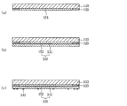
図8の(a)は、ウィンドウ基板110に第1絶縁層151を塗布した図である。
FIG. 8A is a diagram in which the first insulating
第1絶縁層151をプリンティング(Printing)、CVD(Chemical Vaper Deposition)、スパッタリング(Sputtering)、スピンコーティング、スロットダイなどを用いてベゼル120とベゼルとの間を充填する。充填された第1絶縁層151は、有機絶縁膜または無機絶縁膜からなる。この際、第1絶縁層151は、ベゼル120の高さまで充填することが好ましい。しかし、ベゼル120とベゼルとの間に塗布液を充填する過程で塗布液がベゼル120より高すぎる高さに充填されるか、低い高さに充填される工程誤差が頻繁に発生しうる。場合に応じて、工程誤差が後工程に影響を及ぼさない誤差範囲では、第1絶縁層の塗布過程を省略してもよい。この場合、絶縁層は、段差を減少させるか表面の不均一性を解消する役割をする。
The first insulating
第1絶縁層151の高さ(L)は、製品の視認性と製品の厚さおよび製品の収率を考慮して高さを決める。したがって、第1絶縁層151は、0≦L<ベゼルの高さ(BL)×1.3μmの範囲で充填する。第1絶縁層151を積層する工程は、スクリーン印刷方式の工程を用いることが好適である。第1絶縁層151の工程としては、上述のように、スクリーン印刷、ラミネーション、スパッタリング、スロッダイなどの工程を用いてもよい。
The height (L) of the first insulating
図8の(b)は、ウィンドウ基板110に第2絶縁層152を塗布した図である。
FIG. 8B is a diagram in which the second insulating
第2絶縁層152は、第1絶縁層151とベゼルの表面に形成される。第2絶縁層152は、第1絶縁層151と同じ材質と工程を用いて積層する。しかし、場合に応じて、異なる材質および異なる工程を用いて積層してもよい。
The second
第2絶縁層152が第1絶縁層151に形成されると、ウィンドウ基板110の中央点における高さ(d)は、次の式:積層方向における第2絶縁層152の高さ(2L)×0.05μm<中央点における高さ(d)μm≦第2絶縁層の高さ(2L)×1.3μmを満たす。これは、電極パターン140の形成時に電気的信頼性を低下させない範囲を設定したものである。第2絶縁層152は、積層方向における前記第2絶縁層152の高さ(2L)が前記ベゼル120の高さ(BL)に対して3倍の大きさを超えないようにする。これは、製品の厚さが増加することを防止し、タッチセンサ1の収率を改善するためである。
When the second insulating
図8の(c)は、ウィンドウ基板110に電極パターン140を形成した図である。
FIG. 8C is a diagram in which an
電極パターンの材質および関連説明は、前記本発明の一実施例によるタッチセンサ1に係る説明において説明したため、重複する説明は省略する。電極パターンは、絶縁層の表面に形成される。1層構造の電極パターン140を用いて自己静電容量方式(Self Capacitive Type)タッチセンサまたは相互静電容量方式(Mutual Capacitive Type)タッチセンサを製作することができる。また、ベゼル120の非活性領域に、外部に電気的信号を伝達する配線電極が形成される。
Since the material of the electrode pattern and the related description have been described in the description of the
以上、本発明を具体的な実施例に基づいて詳細に説明したが、これは本発明を具体的に説明するためのものであり、本発明はこれに限定されず、該当分野における通常の知識を有する者であれば、本発明の技術的思想内にての変形や改良が可能であることは明白であろう。 As described above, the present invention has been described in detail based on the specific embodiments. However, the present invention is only for explaining the present invention, and the present invention is not limited thereto. It will be apparent to those skilled in the art that modifications and improvements within the technical idea of the present invention are possible.
本発明の単純な変形乃至変更はいずれも本発明の領域に属するものであり、本発明の具体的な保護範囲は添付の特許請求の範囲により明確になるであろう。 All simple variations and modifications of the present invention belong to the scope of the present invention, and the specific scope of protection of the present invention will be apparent from the appended claims.
本発明は、タッチセンサに適用可能である。 The present invention is applicable to a touch sensor.
1 タッチセンサ
110 ウィンドウ基板
111 活性領域
112 非活性領域
120 ベゼル
140 電極パターン
150 絶縁層
151 第1絶縁層
152 第2絶縁層
DESCRIPTION OF
Claims (15)
前記ウィンドウ基板の周縁に沿って形成されるベゼルと、
前記ベゼルとベゼルとの間を充填しながら積層または接着されて、前記ウィンドウ基板上に形成される絶縁層と、
前記絶縁層上に形成される電極パターンと、を含む、タッチセンサ。 A window substrate;
A bezel formed along the periphery of the window substrate;
An insulating layer formed on the window substrate by being laminated or adhered while filling between the bezel and the bezel;
An electrode pattern formed on the insulating layer.
前記ウィンドウ基板の周縁に沿って形成されるベゼルと、
前記ベゼルとベゼルとの間を充填しながら積層され、前記ウィンドウ基板上に形成される第1絶縁層と、
前記ベゼルおよび第1絶縁層上に塗布および接着して形成される第2絶縁層と、
前記第2絶縁層上に形成される電極パターンと、を含む、タッチセンサ。 A window substrate;
A bezel formed along the periphery of the window substrate;
A first insulating layer that is stacked while filling between the bezel and the bezel, and is formed on the window substrate;
A second insulating layer formed by applying and bonding on the bezel and the first insulating layer;
An electrode pattern formed on the second insulating layer.
b)前記ウィンドウ基板の一面に形成され、且つ前記ベゼルとベゼルとの間に第1絶縁層を充填する段階と、
c)前記ベゼルと第1絶縁層を横切って第2絶縁層を形成する段階と、
d)前記第2絶縁層上に電極パターンを形成する段階と、を含む、タッチセンサの製造方法。 a) fixing a window substrate on which a bezel is formed along the periphery;
b) filling a first insulating layer between the bezel and the bezel formed on one surface of the window substrate;
c) forming a second insulating layer across the bezel and the first insulating layer;
d) forming an electrode pattern on the second insulating layer; and a method for manufacturing a touch sensor.
積層方向に形成された前記第1絶縁層の高さ(L)は、次の式:0≦L<(前記ベゼルの高さ(BL)×1.3)μmを満たすことを特徴とする、請求項11に記載のタッチセンサの製造方法。 In step b)
The height (L) of the first insulating layer formed in the stacking direction satisfies the following formula: 0 ≦ L <(height of the bezel (BL) × 1.3) μm, The manufacturing method of the touch sensor of Claim 11.
前記ウィンドウ基板の中央点における高さ(d)は、次の式:(積層方向における前記第2絶縁層の高さ(2L)×0.05)<d<(前記絶縁層の高さ(2L)×1.3)μmを満たすことを特徴とする、請求項12に記載のタッチセンサの製造方法。 In step c),
The height (d) at the center point of the window substrate is given by the following formula: (height of the second insulating layer in the stacking direction (2L) × 0.05) <d <(height of the insulating layer (2L The method for manufacturing a touch sensor according to claim 12, wherein the method satisfies the following formula:) × 1.3) μm.
積層方向における前記第2絶縁層の高さ(2L)は、前記ベゼルの高さ(BL)に対して3倍の大きさを超えないように形成されることを特徴とする、請求項12に記載のタッチセンサの製造方法。 In step c),
The height (2L) of the second insulating layer in the stacking direction is formed so as not to exceed three times the height (BL) of the bezel. The manufacturing method of the touch sensor as described.
前記第2絶縁層は前記第1絶縁層と同じ材質を使用することを特徴とする、請求項14に記載のタッチセンサの製造方法。 In step c),
The method of claim 14, wherein the second insulating layer uses the same material as the first insulating layer.
Applications Claiming Priority (2)
| Application Number | Priority Date | Filing Date | Title |
|---|---|---|---|
| KR10-2013-0081085 | 2013-07-10 | ||
| KR1020130081085A KR20150007107A (en) | 2013-07-10 | 2013-07-10 | Touch sensor |
Publications (1)
| Publication Number | Publication Date |
|---|---|
| JP2015018532A true JP2015018532A (en) | 2015-01-29 |
Family
ID=52276823
Family Applications (1)
| Application Number | Title | Priority Date | Filing Date |
|---|---|---|---|
| JP2013220366A Pending JP2015018532A (en) | 2013-07-10 | 2013-10-23 | Touch sensor |
Country Status (3)
| Country | Link |
|---|---|
| US (1) | US20150015802A1 (en) |
| JP (1) | JP2015018532A (en) |
| KR (1) | KR20150007107A (en) |
Cited By (1)
| Publication number | Priority date | Publication date | Assignee | Title |
|---|---|---|---|---|
| US11093089B2 (en) | 2017-11-15 | 2021-08-17 | Fujifilm Corporation | Touch sensor and touch panel with touch electrodes and insulating layer |
Families Citing this family (6)
| Publication number | Priority date | Publication date | Assignee | Title |
|---|---|---|---|---|
| KR20150087655A (en) * | 2014-01-22 | 2015-07-30 | 삼성디스플레이 주식회사 | Window for display device and display device comprising the same |
| KR102433107B1 (en) * | 2016-01-19 | 2022-08-18 | 삼성디스플레이 주식회사 | Touch display devices |
| CN105807994A (en) * | 2016-03-04 | 2016-07-27 | 京东方科技集团股份有限公司 | Rupture membrane and manufacturing method thereof, touch screen and display device |
| US10898886B2 (en) * | 2016-08-26 | 2021-01-26 | Ford Global Technologies, Llc | Hydrocarbon and nitrogen oxides catalyst trap |
| CN107992238A (en) * | 2017-11-28 | 2018-05-04 | 业成科技(成都)有限公司 | Contact panel module |
| CN109992163B (en) * | 2019-04-15 | 2023-01-03 | 业成科技(成都)有限公司 | Touch sensing module, manufacturing method thereof and electronic device applying touch sensing module |
Citations (5)
| Publication number | Priority date | Publication date | Assignee | Title |
|---|---|---|---|---|
| JP2008197913A (en) * | 2007-02-13 | 2008-08-28 | Alps Electric Co Ltd | Electronic equipment |
| JP2011197708A (en) * | 2010-03-17 | 2011-10-06 | Sony Corp | Method for manufacturing touch panel |
| US20120075209A1 (en) * | 2010-09-29 | 2012-03-29 | Catcher Technology Co., Ltd. | Touch panel |
| JP2012088934A (en) * | 2010-10-20 | 2012-05-10 | Alps Electric Co Ltd | Input device and method for manufacturing input device |
| JP2013003915A (en) * | 2011-06-17 | 2013-01-07 | Toppan Printing Co Ltd | Projected capacitive touch panel sensor, manufacturing method of the same and display device having projected capacitive touch panel sensor |
Family Cites Families (1)
| Publication number | Priority date | Publication date | Assignee | Title |
|---|---|---|---|---|
| TW201416924A (en) * | 2012-10-16 | 2014-05-01 | Wintek Corp | Touch-sensitive display device and fabrication method thereof |
-
2013
- 2013-07-10 KR KR1020130081085A patent/KR20150007107A/en not_active Application Discontinuation
- 2013-10-23 JP JP2013220366A patent/JP2015018532A/en active Pending
- 2013-10-24 US US14/062,243 patent/US20150015802A1/en not_active Abandoned
Patent Citations (5)
| Publication number | Priority date | Publication date | Assignee | Title |
|---|---|---|---|---|
| JP2008197913A (en) * | 2007-02-13 | 2008-08-28 | Alps Electric Co Ltd | Electronic equipment |
| JP2011197708A (en) * | 2010-03-17 | 2011-10-06 | Sony Corp | Method for manufacturing touch panel |
| US20120075209A1 (en) * | 2010-09-29 | 2012-03-29 | Catcher Technology Co., Ltd. | Touch panel |
| JP2012088934A (en) * | 2010-10-20 | 2012-05-10 | Alps Electric Co Ltd | Input device and method for manufacturing input device |
| JP2013003915A (en) * | 2011-06-17 | 2013-01-07 | Toppan Printing Co Ltd | Projected capacitive touch panel sensor, manufacturing method of the same and display device having projected capacitive touch panel sensor |
Cited By (1)
| Publication number | Priority date | Publication date | Assignee | Title |
|---|---|---|---|---|
| US11093089B2 (en) | 2017-11-15 | 2021-08-17 | Fujifilm Corporation | Touch sensor and touch panel with touch electrodes and insulating layer |
Also Published As
| Publication number | Publication date |
|---|---|
| KR20150007107A (en) | 2015-01-20 |
| US20150015802A1 (en) | 2015-01-15 |
Similar Documents
| Publication | Publication Date | Title |
|---|---|---|
| KR101521681B1 (en) | Touch Panel | |
| JP5112492B2 (en) | Transparent conductive film for touch panel and manufacturing method thereof | |
| JP2015018532A (en) | Touch sensor | |
| KR20130078065A (en) | Touch panel | |
| US20150227170A1 (en) | Touch sensor and method for manufacturing the same | |
| JP2013137731A (en) | Touch screen | |
| KR101119355B1 (en) | Touch panel | |
| KR20130051803A (en) | Touch panel | |
| JP2014081910A (en) | Touch panel and manufacturing method of the same | |
| JP2013228985A (en) | Touch panel | |
| JP2015125773A (en) | Touch sensor and method of manufacturing the same | |
| US20140062908A1 (en) | Touch panel and method for manufacturing the same | |
| JP2014049114A (en) | Touch panel | |
| JP2013134768A (en) | Sensing electrode pattern for touch panel | |
| JP2015088185A (en) | Touch sensor | |
| JP2014049113A (en) | Touch panel | |
| JP2013222456A (en) | Touch panel | |
| JP2014120149A (en) | Touch panel | |
| US20150049259A1 (en) | Touch sensor module and manufacturing method thereof | |
| US20140184953A1 (en) | Touch panel | |
| US9383842B2 (en) | Touch sensor module and method of manufacturing the same | |
| JP2014174978A (en) | Display device including touch panel | |
| JP2015170353A (en) | touch sensor | |
| KR20110124509A (en) | Capacitive type touch panel | |
| KR20130051322A (en) | Touch panel |
Legal Events
| Date | Code | Title | Description |
|---|---|---|---|
| A977 | Report on retrieval |
Free format text: JAPANESE INTERMEDIATE CODE: A971007 Effective date: 20150518 |
|
| A131 | Notification of reasons for refusal |
Free format text: JAPANESE INTERMEDIATE CODE: A131 Effective date: 20150602 |
|
| A02 | Decision of refusal |
Free format text: JAPANESE INTERMEDIATE CODE: A02 Effective date: 20151027 |