JP2015073793A - Ultrasonic probe and ultrasonic diagnostic apparatus using the same - Google Patents
Ultrasonic probe and ultrasonic diagnostic apparatus using the same Download PDFInfo
- Publication number
- JP2015073793A JP2015073793A JP2013213015A JP2013213015A JP2015073793A JP 2015073793 A JP2015073793 A JP 2015073793A JP 2013213015 A JP2013213015 A JP 2013213015A JP 2013213015 A JP2013213015 A JP 2013213015A JP 2015073793 A JP2015073793 A JP 2015073793A
- Authority
- JP
- Japan
- Prior art keywords
- cell
- voltage
- cells
- boundary
- lower electrode
- Prior art date
- Legal status (The legal status is an assumption and is not a legal conclusion. Google has not performed a legal analysis and makes no representation as to the accuracy of the status listed.)
- Granted
Links
Images


Landscapes
- Ultra Sonic Daignosis Equipment (AREA)
- Transducers For Ultrasonic Waves (AREA)
Abstract
Description
本発明は、超音波探触子、および、それを用いた超音波診断装置に関するものである。より具体的には、容量検出型超音波トランスデューサ(CMUT:Capacitive Micromachined Ultrasonic Transducer)を用いた超音波探触子、および、超音波診断装置に関する。 The present invention relates to an ultrasonic probe and an ultrasonic diagnostic apparatus using the same. More specifically, the present invention relates to an ultrasonic probe using a capacitive detection type ultrasonic transducer (CMUT) and an ultrasonic diagnostic apparatus.
超音波トランスデューサは、被検体に超音波を送波し、被検体からの反射エコー信号を受波する機能を備えており、人体内の腫瘍などの診断や、構造物の非破壊検査、流体の速度検知などに用いられている。 Ultrasonic transducers have the function of transmitting ultrasonic waves to a subject and receiving reflected echo signals from the subject, diagnosing tumors in the human body, nondestructive inspection of structures, fluid Used for speed detection.
この一例として、容量検出型超音波トランスデューサ(CMUT)が、特許文献1に記載されている。特許文献1において、CMUTを構成するセルには、コンデンサを形成する上部電極と下部電極が設けられている。これらの上下電極間にはバイアス電圧が印加されている。
As an example of this, a capacitance detection type ultrasonic transducer (CMUT) is described in
そして、超音波の送信時には、駆動電圧信号源によって上下電極間に適切な波形(交流)の駆動電圧信号を印加することでメンブレンを振動させ、駆動電圧信号に応じた超音波を発生させる。逆に、超音波の受信時には、CMUTに到達した超音波によってメンブレンが振動することで上下電極間の静電容量が変化し、超音波に応じた電流信号が発生する。この電流信号を検出することで、受信した超音波を検出することができる。 When transmitting an ultrasonic wave, a driving voltage signal source applies a driving voltage signal having an appropriate waveform (alternating current) between the upper and lower electrodes to vibrate the membrane and generate an ultrasonic wave corresponding to the driving voltage signal. Conversely, when receiving an ultrasonic wave, the membrane is vibrated by the ultrasonic wave that reaches the CMUT, whereby the capacitance between the upper and lower electrodes changes, and a current signal corresponding to the ultrasonic wave is generated. By detecting this current signal, the received ultrasonic wave can be detected.
また、特許文献1では、複数のセルを2次元アレイ状に配列してエレメントを構成している。その上で、特に最外周にダミーセルを配列することで、各々のセルにおけるメンブレンの初期変位のばらつきを低減できるとしている。
In
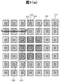
本発明に先立ち、本願発明者らは、CMUTセルが2次元配列されたCMUTアレイにおけるメンブレンの変位量(以下、単に「変位量」と記す)の検討を行った。検討に用いたCMUTアレイのを図1に示す。図1(a)は上面図であり、図1(b)は、図1(a)のA−B線における断面図である。 Prior to the present invention, the present inventors examined the amount of membrane displacement (hereinafter simply referred to as “displacement amount”) in a CMUT array in which CMUT cells are two-dimensionally arranged. The CMUT array used for the study is shown in FIG. 1A is a top view, and FIG. 1B is a cross-sectional view taken along the line AB in FIG. 1A.
図1では、それぞれのCMUTセルが独立した上部電極204と下部電極201を有するものとし、超音波を送受信するセルをONセル206、それ以外のセルをOFFセル207とした。そして、OFFセルに隣接するONセル208とOFFセルに隣接しないONセル209の変位量をシミュレーションし比較した。変位量のシミュレーションは有限要素法により行った。
In FIG. 1, each CMUT cell has an independent
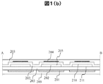
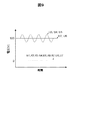
変位量のシミュレーションの結果を図2に示す。なお、図2では、OFFセルに隣接しないONセル208の変位量が1になるよう、変位量を規格化している。図2から、OFFセルに隣接するONセル208の変位量は、OFFセルに隣接しないONセル209より大きくなっていることがわかる。つまり、直流電圧を徐々に増加させていくと、OFFセルに隣接しないONセル209よりも先に、OFFセルに隣接するONセル208において、空洞上面210と下面の空洞下面211が接触することになる。
The result of the displacement amount simulation is shown in FIG. In FIG. 2, the displacement amount is normalized so that the displacement amount of the
空洞上面210が空洞下面211に接触すると、上部電極204と下部電極201に挟まれた絶縁膜203に高電界が印加されて、絶縁膜203の絶縁特性が劣化する。そのため、駆動電圧(直流電圧と交流電圧の合計)は、空洞上面210と空洞下面211が接触しない範囲で設定する必要がある。これに対し、高い送信音圧と受信感度を得るためには、出来る限り大きな電圧を印加し、変位量を大きくすることが望ましい。
When the cavity
すなわち、OFFセルに隣接するONセル208の電圧−変位特性を基に駆動電圧を決定すると、OFFセルに隣接しないONセル209の変位量はOFFセルに隣接するONセル208の変位量よりも小さくなるため、必要な送信音圧と受信感度を得られない恐れがある。反対に、駆動電圧の設定をOFFセルに隣接しないONセル209の電圧−変位特性を基に決定すると、OFFセルに隣接するONセル208の変位量はそれよりも大きいため、OFFセルに隣接するONセル208の空洞上面210と下面の空洞下面211が接触し、絶縁特性を劣化させる恐れがある。
That is, when the drive voltage is determined based on the voltage-displacement characteristic of the
このように、OFFセルに隣接しないONセル209とOFFセルに隣接するONセル208の間に変位量に差があるため、送信音圧および受信感度と絶縁特性とを両立することが困難となる。係る変位量の差を低減する技術については、アレイの境界のセルにしか着目しておらずONセルとOFFセルの隣接関係に着目していない特許文献1はもとより、いずれの先行技術文献にも記載されていない。
Thus, since there is a difference in displacement between the
以上を踏まえ、本願発明の目的は、係る変位量の差をより低減しうる超音波探触子、または、それを用いた超音波診断装置を提供することである。 Based on the above, an object of the present invention is to provide an ultrasonic probe that can further reduce the difference in displacement, or an ultrasonic diagnostic apparatus using the ultrasonic probe.
本発明においては、上記の目的を達成するため、それぞれが、下部電極と、下部電極上に形成された空洞部と、空洞部上に形成された上部電極と、を備え、2次元アレイ状に配列された複数のセルを有し、複数のセルのうち、上部電極と下部電極の間に、直流電圧と交流電圧が重畳された電圧が印加されており、直流電圧および交流電圧の両方が所望の値以上であるセルをONセル、それ以外のセルをOFFセルとするとき、OFFセルのうちONセルと隣接するセルに対して、上部電極と下部電極の間に直流電圧を印加することを特徴とする超音波探触子を提供する。 In the present invention, in order to achieve the above object, each includes a lower electrode, a cavity formed on the lower electrode, and an upper electrode formed on the cavity, in a two-dimensional array. A plurality of cells are arranged, and a voltage in which a DC voltage and an AC voltage are superimposed is applied between the upper electrode and the lower electrode, and both the DC voltage and the AC voltage are desired. When a cell that is greater than or equal to the value of ON cell is set as the ON cell and the other cells are set as the OFF cell, a DC voltage is applied between the upper electrode and the lower electrode for the cells adjacent to the ON cell among the OFF cells. An ultrasonic probe is provided.
本発明によれば、超音波探触子において、OFFセルに隣接しないONセルとOFFセルに隣接するONセルの変位量の差を、より低減することが可能となる。その結果、送信音圧および受信感度と、絶縁特性とを両立することが、より容易となる。 According to the present invention, in the ultrasonic probe, it is possible to further reduce the difference in displacement between the ON cell that is not adjacent to the OFF cell and the ON cell that is adjacent to the OFF cell. As a result, it is easier to achieve both transmission sound pressure and reception sensitivity and insulation characteristics.
以下、本発明の実施例を図面に基づいて詳細に説明する。 Hereinafter, embodiments of the present invention will be described in detail with reference to the drawings.
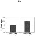
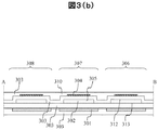
本実施例1に係る超音波探触子を図3を用いて説明する。図3(a)は、本実施例に係る超音波探触子に含まれる超音波トランスデューサの上面図であり、図3(b)は、図3(a)のA−B線における断面図である。図3(b)に図示した通り、上部電極304と下部電極301は、絶縁膜303および空洞部302を介して対向し、静電容量を形成している。以下、本明細書において単に「セルに電圧を印加する」と言った場合は、当該セルの上部電極304と下部電極301の間に当該電圧が印加されていれば良く、上部電極304と下部電極の両者に電位を印加する場合と、上部電極304または下部電極301のいずれか一方に電位を印加する場合とを含む。
The ultrasonic probe according to the first embodiment will be described with reference to FIG. 3A is a top view of the ultrasonic transducer included in the ultrasonic probe according to the present embodiment, and FIG. 3B is a cross-sectional view taken along the line AB of FIG. 3A. is there. As shown in FIG. 3B, the
ここで、ONセル、OFFセルを、以下のように定義する。まず、ONセルを、直流電圧(DC)と交流電圧(AC)が重畳された電圧が印加されており、当該直流電圧および交流電圧の両方が、所望の値以上であるセルと定義する。そして、それ以外のセル、すなわち、当該直流電圧または交流電圧の少なくとも一方が当該所望の値以下のセルを、OFFセルと定義する。例えば、所望の値をAC100V、DC100Vとするとき、(AC100V,DC100V)が印加されているをONセルとし、(AC100V、DC50V)、(AC0V、DC100V)、(AC0V、DC0V)が印加されているセルをOFFセルとする。OFFセルについても、ACが印加されている場合、超音波を発信することはありえるが、この超音波は、ONセルが発信するものと比較して十分小さく、検査の際には無視できる。 Here, the ON cell and the OFF cell are defined as follows. First, an ON cell is defined as a cell to which a voltage in which a direct voltage (DC) and an alternating voltage (AC) are superimposed is applied, and both the direct voltage and the alternating voltage are equal to or higher than a desired value. Then, other cells, that is, cells in which at least one of the DC voltage or the AC voltage is not more than the desired value are defined as OFF cells. For example, when the desired values are AC100V and DC100V, (AC100V, DC100V) is applied as the ON cell, and (AC100V, DC50V), (AC0V, DC100V), (AC0V, DC0V) are applied. The cell is an OFF cell. Also for the OFF cell, when AC is applied, an ultrasonic wave may be transmitted, but this ultrasonic wave is sufficiently smaller than that transmitted by the ON cell, and can be ignored in the inspection.
図3(a)において、ONセルのうち、送受信しないセルに隣接しないセルを非境界ONセル306、隣接するセルを境界ONセル307とする。また、OFFセルのうち、境界ONセル307に隣接するセルを境界OFFセル308、隣接しないセルを非境界OFFセル309とする。、ここでは、非境界ONセル306は1セルとしたが、2セル以上の場合においても同様の効果を得ることができるため、以下では非境界ONセル306が1個の場合を代表例として説明する。
In FIG. 3A, of the ON cells, a cell that is not adjacent to a cell that does not transmit / receive is referred to as a non-boundary ON
本実施例では、ONセル以外に、境界OFFセル308に直流電圧を印加する。このように境界OFFセル308にも直流電圧を印加してメンブレン305を変位させることで、境界ONセル307と非境界ONセル306の間の変位量の差(以下、「変位差」と記す)を低減させることができ、絶縁特性の劣化を抑制する効果を得ることができる。なお、非境界OFFセル309には、直流電圧を印加してもしなくても良い。
In this embodiment, a DC voltage is applied to the boundary OFF
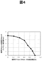
本発明の効果を明らかにするために、境界OFFセル308セルに非境界ONセル306や境界ONセル307と同じ大きさの直流電圧を印加する場合と印加しない場合での、境界ONセル307の変位量を比較した。図4に示すように、境界OFFセルに直流電圧を印加しない場合(境界OFFセル/ONセル 印加直流電圧比がゼロの場合)と比較して、境界OFFセルに直流電圧を印加していくにつれて(図4の右側に行くにつれて)、境界ONセルと非境界ONセルの変位差が低減していることがわかる。また、図4から、少なくとも境界OFFセルに直流電圧を印加しさえすれば変位差を低減する効果があり、特に境界OFFセルにONセルと同じ直流電圧(すなわち、上記「所望の直流電圧」)を印加するときに最も変位差を低減する効果が高い(境界ONセルと非境界ONセルの変位差がゼロになる)ことがわかる。
In order to clarify the effect of the present invention, the boundary ON
ここで、境界OFFセル308に同じ大きさの直流電圧を印加する場合と印加しない場合で境界ONセル307に変位差が生じる原因を調べるために、支持部310に生じる内部応力の計算を行った結果を図5に示す。境界OFFセルに電圧を印加しない場合の方が、電圧を印加した場合よりも、支持部310に生じる引張応力が大きくなっていることがわかる。
Here, in order to investigate the cause of the displacement difference in the boundary ON
この理由は、以下のように説明できる。すなわち、境界OFFセル308に電圧を印加した場合、隣り合って位置する非境界ONセル306と境界ONセル307の両方のメンブレンが変位し、支持部310が両セル方向に引っ張られ、非境界ONセル306の変位量はそれにより減少するように作用する。これに対し、境界OFFセル308に電圧を印加しない場合は、隣接する境界OFFセル308のメンブレンは変位せず、境界ONセル307のメンブレンの変位にのみ引っ張られるため、支持部310の引張応力は支持部310よりも大きくなり、変位量が大きくなる。以上が、境界ONセル307の方が、非境界ONセル306の変位量よりも大きくなる理由である。
The reason for this can be explained as follows. That is, when a voltage is applied to the boundary OFF
以上をまとめると、本実施例に係る超音波探触子は、それぞれが、下部電極301と、下部電極上に形成された空洞部302と、空洞部上に形成された上部電極304と、を備え、2次元アレイ状に配列された複数のセルを有し、複数のセルのうち、上部電極と下部電極の間に、直流電圧と交流電圧が重畳された電圧が印加されており、直流電圧および交流電圧の両方が所望の値以上であるセルをONセル、それ以外のセルをOFFセルとするとき、OFFセルのうちONセルと隣接するセルに対して、上部電極と下部電極の間に直流電圧を印加する。
In summary, the ultrasonic probe according to the present embodiment includes a
係る構成により、本実施例に係る超音波探触子は、境界ONセル307と非境界ONセル306の変位差を低減させることができる。その結果、送信音圧および受信感度と、絶縁特性とを両立することが、より容易となる。
With such a configuration, the ultrasonic probe according to the present embodiment can reduce the displacement difference between the boundary ON
変位差を低減するという観点からは、境界OFFセル308の電極に印加する電圧は非境界ONセル306や境界ONセル307に印加する電圧と同じ大きさが最も効果的であるが、それと異なる大きさの電圧が印加されても良い。
From the viewpoint of reducing the displacement difference, the voltage applied to the electrode of the boundary OFF
本発明において、直流電圧を上部電極304に印加し、下部電極301をグランド電位としても良いし、もしくは直流電圧を下部電極301に印加し、上部電極をグランド電位としても良い。また、本発明において、直流電圧は上部電極304と下部電極301の両方に分割して印加しても良い。例えば、上部電極204と下部電極301の間に100Vの電位差を発生させるために、上部電極304に−50V、下部電極301に+50Vを印加するような方法である。この場合、電圧の極性を反対にして、上部電極304に+50V、下部電極301に−50Vを印加しても良い。
In the present invention, a DC voltage may be applied to the
本実施例では、上部電極および下部電極を複数のセル間で共有するアレイ構造について説明する。上部電極および下部電極を共通化することで、配線の小面積化、電圧印加の効率化等の効果を奏する。その上でさらに、当該アレイ構造に好適な電圧の印加方法について説明する。 In this embodiment, an array structure in which an upper electrode and a lower electrode are shared among a plurality of cells will be described. By using the upper electrode and the lower electrode in common, the effects of reducing the wiring area and increasing the efficiency of voltage application are obtained. Further, a method for applying a voltage suitable for the array structure will be described.
実施例2に係る超音波探触子に含まれる超音波トランスデューサの一例を図6および図7を用いて説明する。図6は、複数のセルが共通の上部電極404と下部電極401を有するアレイ構造を示している。より具体的には、図6のアレイ構造では、第1の方向(図の横方向)に並ぶ複数のセル間で下部電極401(B1〜B7)が共通であり、第1の方向と交差する第2の方向(図の縦方向)に並ぶ複数のセル間で上部電極404(U1〜U7)が共通であるアレイ構造を示している。
An example of an ultrasonic transducer included in the ultrasonic probe according to the second embodiment will be described with reference to FIGS. FIG. 6 shows an array structure in which a plurality of cells have a common
ここで、ONセルのうち、超音波の送受信に使用しないセルに隣接していないセルを非境界ONセル406、隣接しているセルを境界ONセル407とする。また、OFFセルのうち、境界ONセル407に隣接するセルを境界OFFセル408、隣接していないセルを非境界OFFセル409とする。ここでは、非境界ONセル406は1セルとしたが、2セル以上の場合においても同様の効果を得ることができるため、以下では非境界ONセル406は1個の場合を代表例として説明する。本実施例では、非境界ONセル406と境界ONセル407以外に、境界OFFセル408の上部電極404と下部電極401の両方に直流電圧を分割して印加し、メンブレン405を変位させることで、境界ONセル407と非境界ONセル406の変位差を低減させることができる。その結果、送信音圧および受信感度と、絶縁特性とを両立することが、より容易となる。
Here, among the ON cells, a cell that is not adjacent to a cell that is not used for transmission / reception of ultrasonic waves is referred to as a non-border ON
上記の電圧印加方法を以下で具体的に説明する。ここでは、電圧を印加するセルの上部電極404と下部電極401の間にDC100Vの電位差を発生させるために、上部電極にDC+50V、下部電極にDC−50Vを印加する例を用いて説明する。なお、上部電極404にDC−50V、下部電極401にDC+50Vを印加しても同様の効果を得ることができる。
The above voltage application method will be specifically described below. Here, an example will be described in which DC + 50V is applied to the upper electrode and DC-50V is applied to the lower electrode in order to generate a potential difference of DC 100V between the
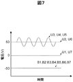
図7に示すとおり、非境界ONセル406、境界ONセル407、境界OFFセル408の上部電極404と下部電極401の間に電圧を印加するために、B2、B3、B4、B5、B6にDC−50Vを、U2、U3、U4、U5、U6にDC+50Vを印加し、U3〜U5には所望のAC電圧を重畳する。U1、U7はグランド電位とする。B1、B7の電位は特に限定されないが、他の下部電極401と等電位にして制御を容易にするため、DC−50Vとする。このような方法で電圧を印加することで、非境界ONセル406、境界ONセル407、境界OFFセル408に対して、上部電極404と下部電極401の間にDC100Vの電位差を発生させることができる。
As shown in FIG. 7, in order to apply a voltage between the
このように、本実施例に係る超音波探触子は、第1の方向に並ぶセル間で下部電極が共通であり第1の方向と交差する第2の方向に並ぶセル間で上部電極が共通であるセルに対し、前記上部電極および前記下部電極の両方に電圧を印加する。係る構成により、本実施例に係る超音波トランスデューサは、境界OFFセル408には所望の電圧を印加して実施例1と同様の効果を奏しつつ、非境界OFFセル409に不必要な電圧が印加されることを防ぐことが可能となり、絶縁特性の劣化を抑制するというさらなる効果を奏するものである。
As described above, in the ultrasonic probe according to the present embodiment, the lower electrode is common between cells arranged in the first direction, and the upper electrode is provided between cells arranged in the second direction intersecting the first direction. For a common cell, a voltage is applied to both the upper electrode and the lower electrode. With this configuration, the ultrasonic transducer according to the present embodiment applies a desired voltage to the boundary OFF
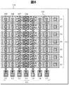
本実施例に係る超音波探触子の他の例を、図8を用いて説明する。図8に示す超音波トランスデューサのアレイ構造は、図6で示したものと同様であるが、相違点は、超音波を送受信する非境界ONセル506、境界ONセル507が第2の方向に一列に並び、ある上部電極(図7の例では、U3、U4、U5)に接続された全てのセルがONセルとなっていることである。この場合に、図7と同様の直流電圧を印加したとすると、非境界ONセル506、境界ONセル507、境界OFFセル508の上部電極504と下部電極501の間には100Vの電位差、非境界OFFセル509には50Vの電位差が生じることになり、少なくとも図6と同程度の絶縁特性の劣化を抑制する効果はある。
Another example of the ultrasonic probe according to the present embodiment will be described with reference to FIG. The array structure of the ultrasonic transducer shown in FIG. 8 is the same as that shown in FIG. 6 except that the non-boundary ON
しかし、図9に示すように、上部電極504のU2、U3、U4、U5、U6に100Vを印加して、上部電極の504のU1、U7と下部電極501のB1、B2、B3、B4、B5、B6、B7をグランド電位とすることにより、OFFセル509には電位差が生じないため、図7で示した直流電圧の印加方法よりも絶縁特性の劣化を抑制する効果が高いことがわかる。すなわち、上部電極のうちいずれか(図8では、U3、U4、U5)に接続されたセルが全てONセルである場合に、境界OFFセル508に対して電圧を印加する際には、境界OFF508セルに接続される上部電極(U2、U6)に所定の電圧を印加し、かつ、境界OFFセルに接続される下部電極(B1、B2、B3、B4、B5、B6、B7)を接地電位とすることで、より絶縁特性の劣化を抑制することが可能となる。なお、非境界ONセル506が1つの上部電極U4のみに接続されたセルである場合を説明したが、例えば上部電極U4とU5に接続されたセル全てが非境界ONセル506である場合であっても同様の効果を得ることができる。
However, as shown in FIG. 9, 100V is applied to U2, U3, U4, U5, U6 of the
図8では、上部電極(U3、U4、U5)に接続された全てのセルがONセル場合について説明したが、下部電極に接続された全てのセルがONセルである場合にも、同様の考え方が適用可能である。すなわち、下部電極のうちいずれかに接続されたセルが全てONセルである場合に、境界OFFセルに対して電圧を印加する際には、境界OFFセルに接続される下部電極に所定の電圧を印加し、かつ、境界OFFセルに接続される上部電極を接地電位とすれば良い。 In FIG. 8, the case where all the cells connected to the upper electrode (U3, U4, U5) are ON cells has been described. However, the same idea can be applied to the case where all the cells connected to the lower electrode are ON cells. Is applicable. That is, when all cells connected to one of the lower electrodes are ON cells, when applying a voltage to the boundary OFF cell, a predetermined voltage is applied to the lower electrode connected to the boundary OFF cell. The upper electrode to be applied and connected to the boundary OFF cell may be set to the ground potential.
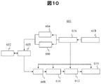
図8を参照しながら、本発明に係る超音波診断装置について説明する。超音波診断装置601は、超音波探触子602、送受分離部603、送信部604、バイアス部606、受信部608、整相加算部610、画像処理部612、表示部614、制御部616、操作部618から構成される。
The ultrasonic diagnostic apparatus according to the present invention will be described with reference to FIG. The ultrasonic
超音波探触子602は、被検体に接触させて被検体との間で超音波を送受波する装置である。超音波探触子602から超音波が被検体に送波され、被検体からの反射エコー信号が超音波探触子602により受波される。実施例1または2の超音波トランスデューサは、超音波探触子602の内部に収納され、後述する送受分離部603と電気的に接続される。送信部604及びバイアス部606は、超音波探触子602に駆動信号を供給する装置である。バイアス部606は、超音波探触子602の電極に駆動電圧を印加する場合とグランド電位とする場合で切り替えるためにスイッチの機能を備えている。また、受信部608は、超音波探触602から出力される反射エコー信号を受信する装置である。受信部608は、さらに、受信した反射エコー信号に対してアナログデジタル変換等の処理を行う。送受分離部603は、送信時には送信部604から超音波探触子602へ駆動信号を渡し、受信時には超音波探触子602から受信部608へ受信信号を渡すよう送信と受信とを切換、分離するものである。整相加算部610は、受信された反射エコー信号を整相加算する装置である。画像処理部610は、整相加算された反射エコー信号に基づいて診断画像(例えば、断層像や血流像)を構成する装置である。表示部614は、画像処理された診断画像を表示する表示装置である。制御部616は、上述した各構成要素を制御する装置であり、駆動電圧を印加する電極の選択し、送信部604及びバイアス部606へ指示を与える機能を有している。操作部618は、制御部616に指示を与える装置である。操作部618は、例えば、トラックボールやキーボードやマウス等の入力機器で構成される。
The
201、301、401、501 下部電極
202、302、405、505 空洞部
203、303 絶縁膜
204、304、404、504 上部電極
205、305 メンブレン
206、306、406、506 ONセル
207、309、409、509 OFFセル
307、407、507 境界ONセル
208 OFFセルに隣接するONセル
209 OFFセルに隣接しないONセル
308、408、508 境界OFFセル
310 指示部
210、312 空洞上面
211、313 空洞下面
601 超音波診断装置
602 超音波探触子
603 送受分離部
604 送信部
606 バイアス部
608 受信部
610 整相加算部
612 画像処理部
614 表示部
616 制御部
618 操作部。
201, 301, 401, 501
206, 306, 406, 506 ON
Claims (7)
前記複数のセルのうち、前記上部電極と前記下部電極の間に、直流電圧と交流電圧が重畳された電圧が印加されており、前記直流電圧および前記交流電圧の両方が所望の値以上であるセルをONセル、それ以外のセルをOFFセルとするとき、
前記OFFセルのうち前記ONセルと隣接するセルに対して、前記上部電極と前記下部電極の間に直流電圧を印加することを特徴とする超音波探触子。 Each comprising a plurality of cells arranged in a two-dimensional array, comprising a lower electrode, a cavity formed on the lower electrode, and an upper electrode formed on the cavity,
Among the plurality of cells, a voltage in which a DC voltage and an AC voltage are superimposed is applied between the upper electrode and the lower electrode, and both the DC voltage and the AC voltage are equal to or higher than desired values. When a cell is an ON cell and other cells are OFF cells,
An ultrasonic probe, wherein a DC voltage is applied between the upper electrode and the lower electrode to a cell adjacent to the ON cell among the OFF cells.
前記OFFセルのうち前記ONセルと隣接するセルに印加される直流電圧は、前記所望の値以上であることを特徴とする超音波探触子。 In claim 1,
The ultrasonic probe, wherein a DC voltage applied to a cell adjacent to the ON cell among the OFF cells is not less than the desired value.
前記複数のセルのうち、第1の方向に並ぶセル間で、前記下部電極は共通であり、
前記複数のセルのうち、前記第1の方向と交差する第2の方向に並ぶセル間で、前記上部電極は共通であることを特徴とする超音波探触子。 In claim 1 or 2,
Among the plurality of cells, the lower electrode is common among the cells arranged in the first direction,
The ultrasonic probe, wherein the upper electrode is common among cells arranged in a second direction intersecting the first direction among the plurality of cells.
前記OFFセルのうち前記ONセルと隣接するセルに対して電圧を印加する際には、前記上部電極と前記下部電極のそれぞれに所定の電圧を印加することを特徴とする超音波探触子。 In claim 3,
An ultrasonic probe characterized in that when a voltage is applied to a cell adjacent to the ON cell among the OFF cells, a predetermined voltage is applied to each of the upper electrode and the lower electrode.
前記下部電極のうちいずれかに接続されたセルが全てONセルである場合に、前記OFFセルに対して電圧を印加する際には、電圧が印加されるOFFセルに接続される下部電極に所定の電圧を印加し、かつ、前記電圧が印加されるOFFセルに接続される上部電極を接地電位とし、
前記上部電極のうちいずれかに接続されたセルが全てONセルである場合に、前記OFFセルに対して電圧を印加する際には、電圧が印加されるOFFセルに接続される上部電極に所定の電圧を印加し、かつ、前記電圧が印加されるOFFセルに接続される下部電極を接地電位とすることを特徴とする超音波探触子。 In claim 3,
When all of the cells connected to any one of the lower electrodes are ON cells, when applying a voltage to the OFF cell, a predetermined value is applied to the lower electrode connected to the OFF cell to which the voltage is applied. The upper electrode connected to the OFF cell to which the voltage is applied is set to the ground potential,
When all of the cells connected to any one of the upper electrodes are ON cells, when applying a voltage to the OFF cell, a predetermined value is applied to the upper electrode connected to the OFF cell to which the voltage is applied. An ultrasonic probe characterized in that the lower electrode connected to the OFF cell to which the voltage is applied is set to the ground potential.
前記ONセルにおいて前記上部電極と前記下部電極の間に印加する直流電圧と、前記OFFセルにおいて前記上部電極と前記下部電極の間に印加する直流電圧とは、等しいことを特徴とする超音波探触子。 In any one of Claims 1 to 5,
An ultrasonic probe characterized in that a DC voltage applied between the upper electrode and the lower electrode in the ON cell is equal to a DC voltage applied between the upper electrode and the lower electrode in the OFF cell. Tentacles.
前記ONセルに交流電圧を印加する送信部と、
前記ONセル、および、電圧が印加される前記OFFセルに直流電圧を印加するバイアス部と、を具備する超音波診断装置。 Each comprising a plurality of cells arranged in a two-dimensional array comprising a lower electrode, a cavity formed on the lower electrode, and an upper electrode formed on the cavity, Among the plurality of cells, a voltage in which a DC voltage and an AC voltage are superimposed is applied between the upper electrode and the lower electrode, and both the DC voltage and the AC voltage are equal to or higher than desired values. When a cell is an ON cell and other cells are OFF cells, a DC voltage is applied between the upper electrode and the lower electrode to the cells adjacent to the ON cell among the OFF cells. An ultrasonic probe that
A transmitter for applying an AC voltage to the ON cell;
An ultrasonic diagnostic apparatus comprising: the ON cell; and a bias unit that applies a DC voltage to the OFF cell to which a voltage is applied.
Priority Applications (1)
| Application Number | Priority Date | Filing Date | Title |
|---|---|---|---|
| JP2013213015A JP6189167B2 (en) | 2013-10-10 | 2013-10-10 | Ultrasonic probe and ultrasonic diagnostic apparatus using the same |
Applications Claiming Priority (1)
| Application Number | Priority Date | Filing Date | Title |
|---|---|---|---|
| JP2013213015A JP6189167B2 (en) | 2013-10-10 | 2013-10-10 | Ultrasonic probe and ultrasonic diagnostic apparatus using the same |
Publications (2)
| Publication Number | Publication Date |
|---|---|
| JP2015073793A true JP2015073793A (en) | 2015-04-20 |
| JP6189167B2 JP6189167B2 (en) | 2017-08-30 |
Family
ID=52999114
Family Applications (1)
| Application Number | Title | Priority Date | Filing Date |
|---|---|---|---|
| JP2013213015A Active JP6189167B2 (en) | 2013-10-10 | 2013-10-10 | Ultrasonic probe and ultrasonic diagnostic apparatus using the same |
Country Status (1)
| Country | Link |
|---|---|
| JP (1) | JP6189167B2 (en) |
Cited By (2)
| Publication number | Priority date | Publication date | Assignee | Title |
|---|---|---|---|---|
| JP2016123064A (en) * | 2014-12-25 | 2016-07-07 | キヤノン株式会社 | Electrostatic capacity type transducer, probe and analyte information acquisition device |
| JP2018522667A (en) * | 2015-08-11 | 2018-08-16 | コーニンクレッカ フィリップス エヌ ヴェKoninklijke Philips N.V. | Capacitive micromachined ultrasonic transducer with increased patient safety |
Citations (4)
| Publication number | Priority date | Publication date | Assignee | Title |
|---|---|---|---|---|
| WO2008136198A1 (en) * | 2007-04-27 | 2008-11-13 | Hitachi, Ltd. | Ultrasonic transducer and ultrasonic imaging apparatus |
| JP2010172181A (en) * | 2008-12-25 | 2010-08-05 | Canon Inc | Electromechanical transducer and production method of same |
| JP2010251847A (en) * | 2009-04-10 | 2010-11-04 | Canon Inc | Mechanical electrical change element |
| JP2011004280A (en) * | 2009-06-19 | 2011-01-06 | Canon Inc | Capacitive electromechanical transducer |
-
2013
- 2013-10-10 JP JP2013213015A patent/JP6189167B2/en active Active
Patent Citations (4)
| Publication number | Priority date | Publication date | Assignee | Title |
|---|---|---|---|---|
| WO2008136198A1 (en) * | 2007-04-27 | 2008-11-13 | Hitachi, Ltd. | Ultrasonic transducer and ultrasonic imaging apparatus |
| JP2010172181A (en) * | 2008-12-25 | 2010-08-05 | Canon Inc | Electromechanical transducer and production method of same |
| JP2010251847A (en) * | 2009-04-10 | 2010-11-04 | Canon Inc | Mechanical electrical change element |
| JP2011004280A (en) * | 2009-06-19 | 2011-01-06 | Canon Inc | Capacitive electromechanical transducer |
Cited By (4)
| Publication number | Priority date | Publication date | Assignee | Title |
|---|---|---|---|---|
| JP2016123064A (en) * | 2014-12-25 | 2016-07-07 | キヤノン株式会社 | Electrostatic capacity type transducer, probe and analyte information acquisition device |
| JP2018522667A (en) * | 2015-08-11 | 2018-08-16 | コーニンクレッカ フィリップス エヌ ヴェKoninklijke Philips N.V. | Capacitive micromachined ultrasonic transducer with increased patient safety |
| US11213855B2 (en) | 2015-08-11 | 2022-01-04 | Koninklijke Philips N.V. | Capacitive micromachined ultrasonic transducers with increased patient safety |
| JP7094217B2 (en) | 2015-08-11 | 2022-07-01 | コーニンクレッカ フィリップス エヌ ヴェ | Capacitive Micromachine Ultrasonic Transducer with Increased Patient Safety |
Also Published As
| Publication number | Publication date |
|---|---|
| JP6189167B2 (en) | 2017-08-30 |
Similar Documents
| Publication | Publication Date | Title |
|---|---|---|
| Sampaleanu et al. | Top-orthogonal-to-bottom-electrode (TOBE) CMUT arrays for 3-D ultrasound imaging | |
| US20160051225A1 (en) | Ultrasonic transducers | |
| CN101874312B (en) | Variable Operating Voltage in Micromachined Ultrasound Transducers | |
| CN103417246B (en) | Ultrasonic transducer, ultrasonic probe, diagnostic device, and electronic instrument | |
| CN105310718B (en) | Ultrasonic devices, detectors and electronics | |
| US20160077058A1 (en) | Ultrasonic detection device and ultrasonic diagnostic device | |
| JPWO2009063964A1 (en) | Ultrasonic imaging device | |
| CN111050930B (en) | Ultrasonic interface element and method | |
| CN104281772A (en) | Transducer and subject information acquisition apparatus | |
| US9770740B2 (en) | Ultrasonic transducer and ultrasonic diagnostic apparatus including the same | |
| CN104013420B (en) | Ultrasonic detector device, head unit, detector and ultrasound imaging device | |
| JP6189167B2 (en) | Ultrasonic probe and ultrasonic diagnostic apparatus using the same | |
| JP2018056734A (en) | Ultrasonic transducer, manufacturing method thereof, and ultrasonic imaging device | |
| JP6782649B2 (en) | Ultrasound imaging device | |
| US20160047780A1 (en) | Methods of operating ultrasonic transducers, and ultrasonic devices | |
| JP6933082B2 (en) | Ultrasonic Transducer and Ultrasonic Diagnostic Device | |
| US11364521B2 (en) | Ultrasonic transducer and ultrasonic probe | |
| JP2019176292A (en) | Ultrasonic sensor and ultrasonic device | |
| JP4776349B2 (en) | Ultrasonic imaging device | |
| JP5957758B2 (en) | Ultrasonic transmitter / receiver and ultrasonic measuring device | |
| JP2019176293A (en) | Ultrasonic sensor and ultrasonic device | |
| CN111107947B (en) | Ultrasonic transducer apparatus and control method thereof | |
| KR20150047003A (en) | Ultrasonic transducer and ultrasonic diagnostic equipment including the same | |
| JP6186737B2 (en) | Ultrasonic measuring device, ultrasonic imaging device, and ultrasonic measuring method | |
| You et al. | Direction of arrival estimation using asymmetric mode components of CMUTs |
Legal Events
| Date | Code | Title | Description |
|---|---|---|---|
| A711 | Notification of change in applicant |
Free format text: JAPANESE INTERMEDIATE CODE: A712 Effective date: 20160603 |
|
| A621 | Written request for application examination |
Free format text: JAPANESE INTERMEDIATE CODE: A621 Effective date: 20160727 |
|
| TRDD | Decision of grant or rejection written | ||
| A01 | Written decision to grant a patent or to grant a registration (utility model) |
Free format text: JAPANESE INTERMEDIATE CODE: A01 Effective date: 20170704 |
|
| A61 | First payment of annual fees (during grant procedure) |
Free format text: JAPANESE INTERMEDIATE CODE: A61 Effective date: 20170802 |
|
| R150 | Certificate of patent or registration of utility model |
Ref document number: 6189167 Country of ref document: JP Free format text: JAPANESE INTERMEDIATE CODE: R150 |
|
| S111 | Request for change of ownership or part of ownership |
Free format text: JAPANESE INTERMEDIATE CODE: R313111 |
|
| R350 | Written notification of registration of transfer |
Free format text: JAPANESE INTERMEDIATE CODE: R350 |
|
| R250 | Receipt of annual fees |
Free format text: JAPANESE INTERMEDIATE CODE: R250 |
|
| R250 | Receipt of annual fees |
Free format text: JAPANESE INTERMEDIATE CODE: R250 |
|
| R250 | Receipt of annual fees |
Free format text: JAPANESE INTERMEDIATE CODE: R250 |
|
| S111 | Request for change of ownership or part of ownership |
Free format text: JAPANESE INTERMEDIATE CODE: R313111 |
|
| R350 | Written notification of registration of transfer |
Free format text: JAPANESE INTERMEDIATE CODE: R350 |
|
| R250 | Receipt of annual fees |
Free format text: JAPANESE INTERMEDIATE CODE: R250 |