JP2015018904A - Mark detection method and device, and exposure method and device - Google Patents
Mark detection method and device, and exposure method and device Download PDFInfo
- Publication number
- JP2015018904A JP2015018904A JP2013144474A JP2013144474A JP2015018904A JP 2015018904 A JP2015018904 A JP 2015018904A JP 2013144474 A JP2013144474 A JP 2013144474A JP 2013144474 A JP2013144474 A JP 2013144474A JP 2015018904 A JP2015018904 A JP 2015018904A
- Authority
- JP
- Japan
- Prior art keywords
- mark
- substrate
- wafer
- pattern
- back surface
- Prior art date
- Legal status (The legal status is an assumption and is not a legal conclusion. Google has not performed a legal analysis and makes no representation as to the accuracy of the status listed.)
- Pending
Links
Images


Abstract
Description
本発明は、基板に設けられたマークを検出するマーク検出技術、そのマーク検出技術を用いる露光技術、及びこの露光技術を用いるデバイス製造技術に関する。 The present invention relates to a mark detection technique for detecting a mark provided on a substrate, an exposure technique using the mark detection technique, and a device manufacturing technique using the exposure technique.
半導体素子等の電子デバイス(マイクロデバイス)を生産するためのフォトリソグラフィ工程で使用される、いわゆるステッパー又はスキャニングステッパーなどの露光装置による露光対象の基板として、円板状の半導体ウエハ(以下、単にウエハという。)がある。電子デバイスを製造する際のスループット(生産性)を高めるために、そのウエハの直径のSEMI(Semiconductor Equipment and Materials International)規格(SEMI standards)は、数年ごとに125mm、150mm、200mm、300mmとほぼ1.25〜1.5倍の割合で大きくなってきている。 As a substrate to be exposed by an exposure apparatus such as a so-called stepper or scanning stepper used in a photolithography process for producing an electronic device (microdevice) such as a semiconductor element, a disk-shaped semiconductor wafer (hereinafter simply referred to as a wafer) There is.) In order to increase the throughput (productivity) when manufacturing electronic devices, the SEMI (Semiconductor Equipment and Materials International) standard (SEMI standards) of the diameter of the wafer is almost 125 mm, 150 mm, 200 mm, and 300 mm every few years. It is increasing at a rate of 1.25 to 1.5 times.
また、従来のウエハのエッジ部には、外形基準で回転角を検出するための切り欠き部としてのノッチ又はオリエンテーションフラットが形成されていた。そして、ウエハを露光装置にロードする際には、予めプリアライメント系によってウエハの切り欠き部の位置を検出しておき、この結果に基づいてウエハの回転角等の大まかな調整を行っていた(例えば、特許文献1参照)。 Further, a notch or an orientation flat as a notch for detecting the rotation angle on the basis of the outer shape is formed at the edge portion of the conventional wafer. When the wafer is loaded into the exposure apparatus, the position of the notch portion of the wafer is detected in advance by a pre-alignment system, and rough adjustment of the rotation angle of the wafer is performed based on this result ( For example, see Patent Document 1).
最近、電子デバイスを製造する際のスループットをより高めるために、SEMI規格では、直径450mmのウエハの規格化が行われている。このように大型化したウエハでは、回転角を検出するための切り欠き部をエッジ部に設けると、ウエハに歪み等が生じる恐れがある。そこで、大型化したウエハでは、回転角を検出するために、裏面に例えば凹部よりなる小さいマークを設けることが検討されている。 Recently, in order to further increase the throughput when manufacturing electronic devices, the SEMI standard has standardized a wafer having a diameter of 450 mm. In such a large wafer, if a notch for detecting the rotation angle is provided at the edge, the wafer may be distorted. In view of this, in order to detect the rotation angle of a large-sized wafer, it has been studied to provide a small mark made of, for example, a recess on the back surface.
これに関して、ウエハは、従来、裏面が支持された状態で露光装置に搬送されており、プリアライメント系は、ウエハの表面(デバイスパターンが形成される面)側からウエハの切り欠き部を検出していたため、従来の技術ではウエハの裏面に設けられたマークの検出を行うことは困難である。さらに、ウエハは多くの工程を経るため、搬送及び/又は加工中の摩耗によるウエハ裏面のマークの消失、又は加工中にウエハの裏面のマークが感光材料又は薄膜に覆われることなどによって、そのマークの検出が困難になる恐れがある。そこで、ウエハの裏面のマークの検出が困難になった場合の対策も考えておくことが好ましい。 In this regard, the wafer is conventionally transported to the exposure apparatus with the back surface supported, and the pre-alignment system detects the notch of the wafer from the front surface (surface on which the device pattern is formed) side of the wafer. For this reason, it is difficult to detect the mark provided on the back surface of the wafer with the conventional technique. Further, since the wafer goes through many processes, the mark on the back surface of the wafer disappears due to wear during conveyance and / or processing, or the mark on the back surface of the wafer is covered with a photosensitive material or thin film during processing. May be difficult to detect. Therefore, it is preferable to consider measures when it becomes difficult to detect the mark on the back surface of the wafer.
本発明の態様は、このような事情に鑑み、基板の裏面にマークが設けられている場合に、そのマークを効率的に検出できるようにするとともに、そのマークの検出が困難になった場合にもその基板の位置情報を検出できるようにすることを目的とする。 In view of such circumstances, the aspect of the present invention enables efficient detection of a mark when the mark is provided on the back surface of the substrate, and makes it difficult to detect the mark. Another object of the present invention is to make it possible to detect positional information of the substrate.
第1の態様によれば、基板に形成されたマークを検出するマーク検出装置であって、裏面に第1マークが形成された基板を一時的に保持する基板保持部と、その基板保持部にその基板が保持されている状態で、その裏面のその第1マークの位置情報を検出する第1検出部と、検出されたその第1マークの位置情報に基づいて、その基板の表面に第2マークを形成するためのマーク形成部と、その第1マークとその第2マークとの位置関係を記憶する記憶部と、その基板保持部にその基板が保持されている状態で、その表面のその第2マークの位置情報を検出する第2検出部と、を備えるマーク検出装置が提供される。 According to the first aspect, there is provided a mark detection device for detecting a mark formed on a substrate, the substrate holding unit temporarily holding the substrate having the first mark formed on the back surface, and the substrate holding unit. In a state where the substrate is held, a first detection unit that detects position information of the first mark on the back surface, and a second surface on the surface of the substrate based on the detected position information of the first mark. A mark forming portion for forming a mark, a storage portion for storing a positional relationship between the first mark and the second mark, and the substrate holding portion holding the substrate, And a second detector that detects position information of the second mark.
第2の態様によれば、基板に形成されたマークを検出するマーク検出装置であって、裏面に第1マークが形成された基板を一時的に保持する基板保持部と、その基板保持部にその基板が保持されている状態で、その裏面のその第1マークの位置情報を検出する第1検出部と、その基板の表面であって該表面の他の領域内のパターン又は反射率分布と識別可能な特徴部の位置情報を検出する第2検出部と、その第1マークとその特徴部との位置関係を記憶する記憶部と、を備えるマーク検出装置が提供される。 According to the second aspect, there is provided a mark detection device for detecting a mark formed on a substrate, the substrate holding unit temporarily holding the substrate having the first mark formed on the back surface, and the substrate holding unit. A first detector for detecting position information of the first mark on the back surface of the substrate while the substrate is held; and a pattern or reflectance distribution on the surface of the substrate in another region of the surface A mark detection device is provided that includes a second detection unit that detects position information of an identifiable feature, and a storage unit that stores a positional relationship between the first mark and the feature.
第3の態様によれば、露光光でパターンを照明し、その露光光でそのパターン及び投影光学系を介して基板を露光する露光装置において、第1の態様のマーク検出装置と、その基板を保持して移動するステージと、そのマーク検出装置によって検出されるその基板の裏面に形成されたその第1マーク又はその基板の表面のその第2マークの位置情報に基づいて、その基板のそのパターンに対する位置及び回転角の少なくとも一方を補正する制御部と、を備える露光装置が提供される。 According to the third aspect, in the exposure apparatus that illuminates the pattern with the exposure light and exposes the substrate with the exposure light through the pattern and the projection optical system, the mark detection apparatus according to the first aspect and the substrate The pattern of the substrate based on the stage that is held and moved, and the position information of the first mark formed on the back surface of the substrate detected by the mark detection device or the second mark on the surface of the substrate An exposure apparatus is provided that includes a control unit that corrects at least one of a position and a rotation angle with respect to.
第4の態様によれば、露光光でパターンを照明し、その露光光でそのパターン及び投影光学系を介して基板を露光する露光装置において、第2の態様のマーク検出装置と、その基板を保持して移動するステージと、そのマーク検出装置によって検出されるその基板の裏面に形成されたその第1マーク又はその基板の表面のその特徴部の位置情報に基づいて、その基板のそのパターンに対する位置及び回転角の少なくとも一方を補正する制御部と、を備える露光装置が提供される。 According to the fourth aspect, in the exposure apparatus that illuminates the pattern with the exposure light and exposes the substrate with the exposure light through the pattern and the projection optical system, the mark detection apparatus according to the second aspect and the substrate Based on the positional information of the stage that is held and moved, and the first mark formed on the back surface of the substrate detected by the mark detection device or the characteristic portion of the surface of the substrate, the pattern of the substrate An exposure apparatus is provided that includes a control unit that corrects at least one of a position and a rotation angle.
第5の態様によれば、基板に形成されたマークを検出するマーク検出方法であって、裏面に第1マークが形成された基板を基板保持部で一時的に保持することと、その基板保持部にその基板が保持されている状態で、その裏面のその第1マークの位置情報を検出することと、検出されたその第1マークの位置情報に基づいて、その基板の表面に第2マークを形成することと、その第1マークとその第2マークとの位置関係を記憶することと、その基板保持部にその基板が保持されている状態で、その表面のその第2マークの位置情報を検出することと、を含むマーク検出方法が提供される。 According to the fifth aspect, there is provided a mark detection method for detecting a mark formed on a substrate, wherein the substrate on which the first mark is formed on the back surface is temporarily held by the substrate holding unit, and the substrate is held. The position information of the first mark on the back surface is detected in a state where the substrate is held by the portion, and the second mark is formed on the surface of the substrate based on the detected position information of the first mark. , Storing the positional relationship between the first mark and the second mark, and the position information of the second mark on the surface in a state where the substrate is held by the substrate holding portion And a mark detection method including:
第6の態様によれば、基板に形成されたマークを検出するマーク検出方法であって、裏面に第1マークが形成された基板を基板保持部で一時的に保持することと、その基板保持部にその基板が保持されている状態で、その裏面のその第1マークの位置情報を検出することと、その基板の表面であって該表面の他の領域内のパターン又は反射率分布と識別可能な特徴部の位置情報を検出することと、その第1マークとその特徴部との位置関係を記憶することと、を含むマーク検出方法が提供される。 According to the sixth aspect, there is provided a mark detection method for detecting a mark formed on a substrate, wherein the substrate on which the first mark is formed on the back surface is temporarily held by the substrate holding unit, and the substrate is held. Detecting the position information of the first mark on the back surface of the substrate while the substrate is held on the surface, and distinguishing it from the pattern or reflectance distribution on the surface of the substrate in other regions of the surface A mark detection method is provided that includes detecting position information of a possible feature and storing a positional relationship between the first mark and the feature.
第7の態様によれば、露光光でパターンを照明し、その露光光でそのパターンを介して基板を露光する露光方法において、第5の態様のマーク検出方法を用いてその基板の裏面に形成されたその第1マーク又はその基板の表面に形成されたその第2マークの位置情報を検出することと、その基板をステージに載置することと、そのマーク検出方法によって検出された位置情報に基づいて、その基板のそのパターンに対する位置及び回転角の少なくとも一方を補正することと、を含む露光方法が提供される。 According to the seventh aspect, in the exposure method of illuminating a pattern with exposure light and exposing the substrate through the pattern with the exposure light, the pattern is formed on the back surface of the substrate using the mark detection method of the fifth aspect. Detecting the position information of the first mark or the second mark formed on the surface of the substrate, placing the substrate on the stage, and the position information detected by the mark detection method. Based on this, there is provided an exposure method including correcting at least one of a position and a rotation angle of the substrate with respect to the pattern.
第8の態様によれば、露光光でパターンを照明し、その露光光でそのパターンを介して基板を露光する露光方法において、第6の態様のマーク検出方法を用いてその基板の裏面に形成されたその第1マーク又はその基板の表面のその特徴部の位置情報を検出することと、その基板をステージに載置することと、そのマーク検出方法によって検出された位置情報に基づいて、その基板のそのパターンに対する位置及び回転角の少なくとも一方を補正することと、を含む露光方法が提供される。 According to an eighth aspect, in the exposure method of illuminating a pattern with exposure light and exposing the substrate through the pattern with the exposure light, the pattern is formed on the back surface of the substrate using the mark detection method of the sixth aspect. Detecting the position information of the first mark or the feature of the surface of the substrate, placing the substrate on the stage, and based on the position information detected by the mark detection method, And correcting at least one of a position and a rotation angle of the substrate with respect to the pattern.
第9の様態によれば、本発明の態様の露光装置又は露光方法を用いて基板上に感光層のパターンを形成することと、そのパターンが形成されたその基板を処理することと、を含むデバイス製造方法が提供される。 According to a ninth aspect, the method includes forming a pattern of a photosensitive layer on a substrate using the exposure apparatus or the exposure method according to the aspect of the present invention, and processing the substrate on which the pattern is formed. A device manufacturing method is provided.
本発明の態様によれば、基板保持部に基板が保持されている状態で、その基板の裏面の第1マークの位置情報を検出しているため、その第1マークを効率的に検出できる。また、基板の表面の第2マーク又は特徴部とその第1マークとの位置関係を記憶しているため、その第1マークの検出が困難になった場合でも、その第2マーク又は特徴部を検出することで、その基板の位置情報を検出できる。 According to the aspect of the present invention, since the position information of the first mark on the back surface of the substrate is detected while the substrate is held by the substrate holding portion, the first mark can be detected efficiently. Further, since the positional relationship between the second mark or feature on the surface of the substrate and the first mark is stored, even if it becomes difficult to detect the first mark, the second mark or feature is not displayed. By detecting, the position information of the substrate can be detected.
[第1の実施形態]
本発明の第1の実施形態につき図1〜図9(F)を参照して説明する。図1は、本実施形態に係るマーク検出装置を備えた露光装置EXの概略構成を示す。露光装置EXは、スキャニングステッパー(スキャナー)よりなる走査露光型の投影露光装置である。露光装置EXは、投影光学系PL(投影ユニットPU)を備えている。以下、投影光学系PLの光軸AXと平行にZ軸を取り、これに直交する面内でレチクルRとウエハ(半導体ウエハ)Wとが相対走査される方向にY軸を、Z軸及びY軸に直交する方向にX軸を取って説明する。また、X軸、Y軸、及びZ軸に平行な軸の回りの回転方向をθx、θy、及びθz方向とも称する。本実施形態では、Z軸に直交する平面(XY平面)はほぼ水平面に平行である。
[First Embodiment]
A first embodiment of the present invention will be described with reference to FIGS. FIG. 1 shows a schematic configuration of an exposure apparatus EX provided with a mark detection apparatus according to the present embodiment. The exposure apparatus EX is a scanning exposure type projection exposure apparatus composed of a scanning stepper (scanner). The exposure apparatus EX includes a projection optical system PL (projection unit PU). Hereinafter, the Z axis is taken in parallel to the optical axis AX of the projection optical system PL, the Y axis is set in the direction in which the reticle R and the wafer (semiconductor wafer) W are relatively scanned in a plane orthogonal to the Z axis, the Z axis and the Y axis. The description will be made by taking the X axis in a direction perpendicular to the axis. In addition, the rotation directions around the axes parallel to the X axis, the Y axis, and the Z axis are also referred to as θx, θy, and θz directions. In the present embodiment, the plane orthogonal to the Z axis (XY plane) is substantially parallel to the horizontal plane.
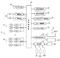
露光装置EXは、例えば米国特許出願公開第2003/0025890号明細書などに開示される照明系ILSと、照明系ILSからの露光用の照明光(露光光)IL(例えば波長193nmのArFエキシマレーザ光、又は固体レーザ(半導体レーザなど)の高調波など)により照明されるレチクルR(マスク)を保持して移動するレチクルステージRSTとを備えている。さらに、露光装置EXは、レチクルRから射出された照明光ILでウエハW(基板)を露光する投影光学系PLを含む投影ユニットPUと、ウエハWを保持して移動するウエハステージWSTと、ウエハWのマークの位置情報(角度情報を含む、以下同様)を含むウエハWの位置情報を検出するプリアライメント系としてのマーク検出装置8と、装置全体の動作を制御するコンピュータよりなる主制御装置20(図3参照)等とを備えている。また、レチクルステージRST及びウエハステージWSTの位置は、上記のX軸、Y軸、及びZ軸よりなる座標系(X,Y,Z)で規定されるため、この座標系(X,Y,Z)をステージ座標系とも称する。
The exposure apparatus EX includes, for example, an illumination system ILS disclosed in, for example, US Patent Application Publication No. 2003/0025890, and illumination light (exposure light) IL (for example, an ArF excimer laser having a wavelength of 193 nm) from the illumination system ILS. A reticle stage RST that holds and moves a reticle R (mask) illuminated by light or a harmonic of a solid-state laser (such as a semiconductor laser). Further, the exposure apparatus EX includes a projection unit PU including a projection optical system PL that exposes the wafer W (substrate) with the illumination light IL emitted from the reticle R, a wafer stage WST that holds and moves the wafer W, and a wafer. A
レチクルRはレチクルステージRSTの上面に真空吸着等により保持され、レチクルRのパターン面(下面)には、回路パターンなどが形成されている。本実施形態では、レチクルステージRSTのレチクルRに対してY方向(走査方向)にずれた位置に、補助レチクルRA(補助マスク)が固定され、補助レチクルRAのパターン面(下面)の例えば中央に、後述のウエハWの裏面のマークの代替マークとして使用可能なマークを形成するための代替マーク用パターン21が形成されている。代替マーク用パターン21は、一例として、X方向に所定間隔で配列された複数のY方向に細長い開口パターンと、Y方向に所定間隔で配列された複数のX方向に細長い開口パターンとを組み合わせた2次元の位置を規定可能なパターンである。レチクルステージRSTは、例えばリニアモータ等を含む図3のレチクルステージ駆動系25によって、不図示のレチクルベース上のXY平面内で微少駆動可能であると共に、走査方向(Y方向)に指定された走査速度で駆動可能である。
The reticle R is held on the upper surface of the reticle stage RST by vacuum suction or the like, and a circuit pattern or the like is formed on the pattern surface (lower surface) of the reticle R. In the present embodiment, the auxiliary reticle RA (auxiliary mask) is fixed at a position shifted in the Y direction (scanning direction) with respect to the reticle R of the reticle stage RST, and is located at, for example, the center of the pattern surface (lower surface) of the auxiliary reticle RA. A
レチクルステージRSTの移動面内の位置情報(X方向、Y方向の位置、及びθz方向の回転角を含む)は、レーザ干渉計よりなるレチクル干渉計24によって、移動鏡22(又は鏡面加工されたステージ端面)を介して例えば0.5〜0.1nm程度の分解能で常時検出される。レチクル干渉計24の計測値は、図3の主制御装置20に送られる。主制御装置20は、その計測値に基づいてレチクルステージ駆動系25を制御することで、レチクルステージRSTの位置及び速度を制御する。
Position information within the moving surface of the reticle stage RST (including the position in the X direction, the Y direction, and the rotation angle in the θz direction) is transferred to the moving mirror 22 (or mirror-finished) by the
図1において、レチクルステージRSTの下方に配置された投影ユニットPUは、鏡筒40と、鏡筒40内に所定の位置関係で保持された複数の光学素子を有する投影光学系PLとを含む。不図示のフレーム機構に対して複数の防振装置(不図示)を介して平板状のフレーム(以下、計測フレームという)16が支持されており、投影ユニットPUは、計測フレーム16に形成された開口内にフランジ部FLを介して設置されている。投影光学系PLは、例えば両側(又はウエハ側に片側)テレセントリックで所定の投影倍率β(例えば1/4倍、1/5倍などの縮小倍率)を有する。
In FIG. 1, the projection unit PU disposed below the reticle stage RST includes a
照明系ILSからの照明光ILによってレチクルRの照明領域IARが照明されると、レチクルRを通過した照明光ILにより、投影光学系PLを介して照明領域IAR内の回路パターンの像が、ウエハWの一つのショット領域の露光領域IA(照明領域IARと光学的に共役な領域)に形成される。ウエハWは、一例としてシリコン等の半導体よりなる直径が450mmの大型の円板状の基材SUにフォトレジストPR(感光材料)を数10〜200nm程度の厚さで塗布したものである(図4(C)参照)。すなわち、一例としてウエハWは450mmウエハである。直径450mmの基材の厚さは、現在では例えば900〜1100μm程度(例えば925μm程度)と想定されている。 When the illumination area IAR of the reticle R is illuminated by the illumination light IL from the illumination system ILS, the image of the circuit pattern in the illumination area IAR is projected via the projection optical system PL by the illumination light IL that has passed through the reticle R. It is formed in an exposure area IA (an area optically conjugate with the illumination area IAR) of one shot area of W. For example, the wafer W is obtained by applying a photoresist PR (photosensitive material) with a thickness of about several tens to 200 nm to a large disk-shaped substrate SU made of a semiconductor such as silicon and having a diameter of 450 mm (FIG. 10). 4 (C)). That is, as an example, the wafer W is a 450 mm wafer. The thickness of a substrate having a diameter of 450 mm is currently assumed to be, for example, about 900 to 1100 μm (for example, about 925 μm).
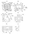
ウエハWが450mmウエハである場合、図4(A)に示すように、ウエハWの円形のエッジ部に切り欠き部を設けない形態も検討されている。すなわち、図4(A)に示すウエハWでは、上記したエッジ部にノッチやオリエンテーションフラットなどの切り欠き部は設けられていない。この場合、ウエハWの表面Wa(基材SUのフォトレジストPRが塗布された面)は、縦横に規則的に多数のショット領域SAに区画され、各ショット領域SAにそれぞれデバイスパターンDPが形成される。ショット領域SAが例えば幅26mm程度で長さ33mm程度の大きさであれば、ウエハWの表面Waには例えば180個程度のショット領域SAが形成される。なお、ウエハWの1回目の露光に際しては、ウエハWの表面Waはショット領域SAには区画されていない。 When the wafer W is a 450 mm wafer, as shown in FIG. 4A, a form in which a notch portion is not provided in the circular edge portion of the wafer W has been studied. That is, in the wafer W shown in FIG. 4A, notches such as notches and orientation flats are not provided in the edge portions described above. In this case, the surface Wa of the wafer W (the surface on which the photoresist PR of the substrate SU is applied) is regularly divided into a large number of shot areas SA vertically and horizontally, and a device pattern DP is formed in each shot area SA. The If the shot area SA is about 26 mm wide and about 33 mm long, for example, about 180 shot areas SA are formed on the surface Wa of the wafer W, for example. In the first exposure of the wafer W, the surface Wa of the wafer W is not partitioned into the shot area SA.
また、ウエハWの表面Waに対向する面、又はウエハWの基材SUのフォトレジストPRが塗布されていない面をウエハWの裏面Wbと称する。図4(B)は、ウエハWの裏面Wbの一部を示し、図4(C)は図4(B)の断面図である。図4(B)、図4(C)に示すように、ウエハWが450mmウエハである場合、ウエハWの裏面Wbのエッジ部Wfから例えば1mmから数mm程度までの周縁領域47内に、ウエハWの半径方向に沿って一列の複数の小さい凹部46aよりなるマーク46を形成する。一例として、凹部46aは直径が100μm程度の円形であって、その深さが20〜70μm程度である。図4(C)では、凹部46aは円柱状であるが、凹部46aは半球面状でもよい。一例として、マーク46の方向(複数の凹部46aの中心を通る直線に沿った方向)は、ウエハWの基材SUの一つの結晶軸の方向に対して所定の角度に、例えば平行に設定してもよい。また、マーク46の方向とウエハWの表面のショット領域SAの長手方向(又は短手方向)とが平行になるように、ショット領域SAを形成してもよい。
Further, a surface facing the front surface Wa of the wafer W or a surface of the base material SU of the wafer W on which the photoresist PR is not applied is referred to as a back surface Wb of the wafer W. 4B shows a part of the back surface Wb of the wafer W, and FIG. 4C is a cross-sectional view of FIG. As shown in FIGS. 4B and 4C, when the wafer W is a 450 mm wafer, the wafer W is located within the
一例として、マーク46は、微小なドリルによる切削、又は加工用レーザ光の照射によって形成できる。さらに、マーク46は、ウエハWの裏面Wbに対する部分的なフォトレジストの塗布、マーク用パターンの露光、現像、エッチング、及びレジスト剥離を含むリソグラフィ工程で形成することも可能である。なお、マーク46において、複数の凹部46aを半径方向に複数列形成してもよい。さらに、マーク46は、複数の凹部46aをウエハWのエッジ部に平行な円周方向に一列に又は複数列に形成したものでもよい。また、マーク46の代わりに、図4(D)に示すように、複数の凹部をウエハWの半径方向に並べた複数列(一列でもよい)の部分マーク46A1,46A2と、複数の凹部をウエハWの円周方向に並べた一列(又は複数列)のマーク部46A3とを含むマーク46Aを使用してもよい。さらに、マーク46の代わりに、図4(E)に示すように、ウエハWの半径方向(又は円周方向)に沿って並べた1本又は複数本の細長い凹部よりなるマーク46Bを使用してもよい。
As an example, the
なお、本実施形態ではウエハWの裏面Wbの一箇所にマーク46を形成しているが、マーク46の個数は特に限定はなく、例えば3つなど複数のマーク46形成してもよい。また、複数のマーク46が裏面Wbに形成される場合には、それぞれのマークを見分けるため形状を異ならせることが好ましい。例えば図4(D)に示すマーク46が裏面Wbに複数させる場合には、各マーク46のうちマーク部46A3の高さ(ウエハWのエッジからの距離)を異ならせることなどが考えられる。これによりウエハWの裏面Wbに複数形成された各マーク46を個別に判別することが可能となる。また、例えば図4(B)のマーク46に、図4(D)で示したマーク部46A3を追加した形状のマークを裏面Wbに複数形成する場合には、上記と同様に各マーク46のうちマーク部46A3の高さ(ウエハWのエッジからの距離)を異ならせることが望ましい。
In this embodiment, the
図1の露光装置EXにおいて、液浸法を適用した露光を行うため、投影光学系PLを構成する最も像面側(ウエハW側)の光学素子である先端レンズ91を保持する鏡筒40の下端部の周囲を取り囲むように、局所液浸装置38の一部を構成するノズルユニット32が設けられている。ノズルユニット32は、露光用の液体Lq(例えば純水)を供給するための供給管31A及び回収管31Bを介して、液体供給装置34及び液体回収装置36(図3参照)に接続されている。なお、液浸タイプの露光装置としない場合には、上記の局所液浸装置38は設けなくともよい。
In the exposure apparatus EX of FIG. 1, in order to perform exposure using the liquid immersion method, the
また、露光装置EXは、レチクルRのアライメントを行うためにレチクルRのアライメントマーク(レチクルマーク)の投影光学系PLによる像の位置を計測する空間像計測系(不図示)と、ウエハWのアライメントを行うために使用される例えば画像処理方式(FIA系)のアライメント系ALと、照射系90a及び受光系90bよりなりウエハWの表面の複数箇所のZ位置を計測する斜入射方式の多点のオートフォーカスセンサ(以下、多点AF系という)90(図3参照)と、ウエハステージWSTの位置情報を計測するためのエンコーダ6(図3参照)と、を備えている。空間像計測系は例えばウエハステージWST内に設けられている。アライメント系ALは、ウエハWの2層目以降のレイヤに露光する際に、ウエハWの表面Waの各ショット領域SAに付設されたアライメントマーク(ウエハマーク)のうちから選択された所定のウエハマークの位置を検出するために使用される。
The exposure apparatus EX also aligns the wafer W with an aerial image measurement system (not shown) that measures the position of the image of the alignment mark (reticle mark) of the reticle R by the projection optical system PL in order to align the reticle R. For example, an image processing system (FIA system) alignment system AL, an
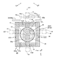
アライメント系ALは、図2に示すように、一例として投影光学系PLに対して−Y方向に離れて配置されたウエハWの直径程度の長さの領域に、X方向(非走査方向)にほぼ等間隔で配列された5眼のアライメント系ALc,ALb,ALa,ALd,ALeから構成され、5眼のアライメント系ALa〜ALeで同時にウエハWの異なる位置のウエハマークを検出できるように構成されている。また、アライメント系ALa〜ALeに対して−Y方向に離れた位置で、かつある程度−X方向及び+X方向にシフトした位置に、それぞれウエハWをロードするときのウエハステージWSTの中心位置であるローディング位置LP、及びウエハWをアンロードするときのウエハステージWSTの中心位置であるアンローディング位置UPが設定されている。ローディング位置LPの上方(+Z方向)に、図1に示すように、ウエハ受け渡し装置66が配置されている。
As shown in FIG. 2, the alignment system AL is, for example, in the X direction (non-scanning direction) in a region about the diameter of the wafer W arranged away from the projection optical system PL in the −Y direction. Consists of five-lens alignment systems ALc, ALb, ALa, ALd, and ALe arranged at approximately equal intervals, and is configured so that wafer marks at different positions on the wafer W can be detected simultaneously by the five-lens alignment systems ALa to ALe. ing. In addition, the loading that is the center position of wafer stage WST when loading wafer W at a position away from −Y direction with respect to alignment systems ALa to ALe and shifted to −X direction and + X direction to some extent. The position LP and the unloading position UP, which is the center position of the wafer stage WST when the wafer W is unloaded, are set. As shown in FIG. 1, a
図1において、ウエハ受け渡し装置66の本体部67は、一例として計測フレーム16とは独立に支持されたフレーム部材FR1に、Z方向に移動可能に支持されている。また、ローディング位置LPの近くに、コータ・デベロッパ(不図示)側から露光装置EXにウエハWを搬入するウエハ搬送ロボットWLDが設置されている。ウエハ搬送ロボットWLDは、一例として、床面に設置された本体部64と、本体部64に対して順次回転可能に設けられた第1及び第2の中間アーム63,62と、第2の中間アーム62の先端部に回転可能に設けられるとともに、ウエハWを真空吸着で保持して搬送するフォーク形の搬送アーム61(図8(A)参照)とを有する。ウエハ搬送ロボットWLDの搬送アーム61は、−Y方向側に設置された回転テーブル(不図示)に載置されたウエハWをウエハ受け渡し装置66の下方まで搬送する。ウエハ受け渡し装置66及びウエハ搬送ロボットWLDの動作は搬送制御系50(図3参照)によって制御される。
In FIG. 1, a
また、ウエハ受け渡し装置66の本体部67の周囲に、ウエハWの裏面に形成されたマーク46(図4(B)参照)及びこの近傍のエッジ部の位置情報(角度情報を含む、以下同様)を検出するマーク検出部52、並びにウエハWの互いに異なる2箇所のエッジ部の位置情報を検出する2つのエッジ検出部53A,53Bが配置されている。一例として、マーク検出部52は、図4(A)及び(B)に示すウエハWの裏面の被検領域でマーク46の像を撮像すると同時に、マーク46の近傍のウエハWのエッジ部の像を撮像する。図4(A)のマーク検出部52による被検領域FVBは、実質的にウエハWの裏面のマーク46を含む第1の被検領域(第1の視野)、及びそのマーク46の近傍のエッジ部を含む第2の被検領域(第2の視野)を合わせた領域である。エッジ検出部53A,53Bは、被検領域FVBとともにウエハWのエッジ部をほぼ等角度間隔で分割した位置にある2つの被検領域(視野)FVA2,FVA1でウエハWのエッジ部の像を撮像する。
Further, the mark 46 (see FIG. 4B) formed on the back surface of the wafer W around the
本実施形態では、マーク検出部52及びエッジ検出部53A,53Bは、それぞれウエハWのエッジ部の近傍のウエハWの表面にあるパターン及びある領域内の反射率分布をも検出可能である。マーク検出部52及びエッジ検出部53A,53Bの検出信号は演算部55(図3参照)に供給される。演算部55は、それらの検出信号を処理してウエハWの中心のX方向、Y方向の位置、及びウエハWの回転角(例えばウエハWのマーク46に平行な方向と、ステージ座標系(X,Y,Z)のY軸に平行な軸とがなす角度)を算出し、算出結果を主制御装置20に供給する。演算部55には磁気記憶装置等の記憶部56が接続されている。
In the present embodiment, the
照明系ILS、補助レチクルRAを備えるレチクルステージRST、及び投影光学系PLを含んで、ウエハWのエッジ部の近傍のウエハWの表面に、ウエハWの裏面のマーク46の代替マークを形成するためのパターン21の像を露光する露光部よりなるマーク形成部が構成されている。この露光部、ウエハ受け渡し装置66、搬送制御系50、マーク検出部52、エッジ検出部53A,53B、演算部55、及び記憶部56を含んで、マーク検出装置8が構成されている。主制御装置20は、演算部55から供給されるウエハWの中心位置及び回転角を用いて、例えばウエハWの大まかな位置及び回転角の補正であるプリアライメントを行うことができる。マーク検出装置8の詳細な構成及び動作については後述する。なお、搬送制御系50及び演算部55は、主制御装置20を構成するコンピュータのソフトウェア上の互いに異なる機能であってもよい。
In order to form a substitute mark for the
さらに、図2のアンローディング位置UPの上方には、ウエハWの搬出時に使用される別のウエハ受け渡し装置(不図示)が配置され、アンローディング位置UPの近くには、搬出(アンロード)されたウエハWをコータ・デベロッパ側に搬出する別のウエハ搬送ロボット(不図示)が配置されている。なお、ウエハ受け渡し装置66によってその搬出用のウエハ受け渡し装置を兼用することも可能である。
Further, another wafer delivery device (not shown) used when unloading the wafer W is disposed above the unloading position UP in FIG. 2, and unloaded near the unloading position UP. Another wafer transfer robot (not shown) for unloading the wafer W to the coater / developer side is arranged. The
また、図2において、多点AF系90の照射系90a及び受光系90bは、一例としてアライメント系ALa〜ALeと投影光学系PLとの間の領域に沿って配置されている。この構成によって、ローディング位置LPでウエハWをウエハステージWSTにロードした後、ウエハステージWSTを駆動して、ウエハWをから投影光学系PLの下方の露光開始位置までほぼY方向に移動することによって、多点AF系90によるウエハ表面のZ位置の分布の計測、及びアライメント系ALa〜ALeによるウエハ表面の複数のウエハマークの位置計測を効率的に行うことができる。多点AF系90及びアライメント系ALの計測結果は主制御装置20に供給される。
In FIG. 2, the
図1において、ウエハステージWSTは、不図示の複数の例えば真空予圧型空気静圧軸受(エアパッド)を介して、ベース盤WBのXY平面に平行な上面WBaに非接触で支持されている。ウエハステージWSTは、例えば平面モータ、又は直交する2組のリニアモータを含むステージ駆動系18(図3参照)によってX方向及びY方向に駆動可能である。ウエハステージWSTは、X方向、Y方向に駆動されるステージ本体30と、ステージ本体30上に搭載されたZステージ部としてのウエハテーブルWTBと、ステージ本体30内に設けられて、ステージ本体30に対するウエハテーブルWTBのZ位置、及びθx方向、θy方向のチルト角を相対的に微小駆動するZステージ駆動部とを備えている。ウエハテーブルWTBの中央の開口の内側には、ウエハWを真空吸着等によってほぼXY平面に平行な載置面上に保持するウエハホルダ44が設けられている。
In FIG. 1, wafer stage WST is supported in a non-contact manner on an upper surface WBa parallel to the XY plane of base board WB via a plurality of unillustrated vacuum preload type static air bearings (air pads), for example. Wafer stage WST can be driven in the X and Y directions by a stage drive system 18 (see FIG. 3) including, for example, a planar motor or two sets of orthogonal linear motors. Wafer stage WST is provided in stage
本実施形態では、ウエハステージWSTのウエハテーブルWTB及びウエハホルダ44を含む部分(Zステージ部)は、ステージ本体30に対してθz方向に指定された角度だけ回転可能に構成されている。主制御装置20がステージ駆動系18を介してそのZステージ部のθz方向の回転角を制御する。なお、Zステージ部のみを回転するのではなく、ステージ本体30及びZステージ部を全体としてθz方向に回転するようにしてもよい。
In the present embodiment, a portion (Z stage portion) including wafer table WTB and
また、ウエハテーブルWTBの上面には、ウエハWの表面とほぼ同一面となる、液体Lqに対して撥液化処理された表面を有し、かつ外形(輪郭)が矩形でその中央部にウエハWの載置領域よりも一回り大きな円形の開口が形成された高い平面度の平板状のプレート体28が設けられていてもよい。
なお、上述の局所液浸装置38を設けたいわゆる液浸型の露光装置の構成にあっては、プレート体28は、さらに図2に示されるように、その円形の開口28aを囲む、外形(輪郭)が矩形で、表面に撥液化処理が施されたプレート部(撥液板)28b、及びプレート部28bを囲む周辺部28eを有する。周辺部28eの上面に、プレート部28bをY方向に挟むようにX方向に細長い1対の2次元の回折格子12A,12Bが固定され、プレート部28bをX方向に挟むようにY方向に細長い1対の2次元の回折格子12C,12Dが固定されている。回折格子12A〜12Dは、それぞれX方向、Y方向を周期方向とする周期が1μm程度の2次元の格子パターンが形成された反射型の回折格子である。
Further, the upper surface of wafer table WTB has a surface that is substantially flush with the surface of wafer W and has been subjected to a liquid repellency treatment with respect to liquid Lq, and has a rectangular outer shape (contour) and a central portion of wafer W. A
In the configuration of the so-called immersion type exposure apparatus provided with the above-mentioned
図1において、計測フレーム16の底面に、投影光学系PLをX方向に挟むように、回折格子12C,12Dに計測用のレーザ光(計測光)を照射して、回折格子に対するX方向、Y方向、Z方向の3次元の相対位置を計測するための複数の3軸の検出ヘッド14が固定されている。さらに、計測フレーム16の底面に、投影光学系PLをY方向に挟むように、回折格子12A,12Bに計測用のレーザ光を照射して、回折格子に対する3次元の相対位置を計測するための複数の3軸の検出ヘッド14が固定されている(図2参照)。さらに、複数の検出ヘッド14にレーザ光(計測光及び参照光)を供給するための一つ又は複数のレーザ光源(不図示)も備えられている。
In FIG. 1, the measurement grating 16 is irradiated with measurement laser light (measurement light) on the diffraction gratings 12 </ b> C and 12 </ b> D so that the projection optical system PL is sandwiched in the X direction on the bottom surface of the
図2において、投影光学系PLを介してウエハWを露光している期間では、Y方向の一列A1内のいずれか2つの検出ヘッド14は、回折格子12A又は12Bに計測光を照射し、回折格子12A,12Bから発生する回折光と参照光との干渉光の検出信号を対応する計測演算部42(図3参照)に供給する。これと並列に、X方向の一行A2内のいずれか2つの検出ヘッド14は、回折格子12C又は12Dに計測光を照射し、回折格子12C,12Dから発生する回折光と参照光との干渉光の検出信号を対応する計測演算部42(図3参照)に供給する。これらの一列A1及び一行A2の検出ヘッド14用の計測演算部42では、ウエハステージWST(ウエハW)と計測フレーム16(投影光学系PL)とのX方向、Y方向、Z方向の相対位置(相対移動量)を例えば0.5〜0.1nmの分解能で求め、それぞれ求めた計測値を切り替え部92A及び92Bに供給する。計測値の切り替え部92A,92Bでは、回折格子12A〜12Dに対向している検出ヘッド14に対応する計測演算部42から供給される相対位置の情報を主制御装置20に供給する。
In FIG. 2, during the period in which the wafer W is exposed through the projection optical system PL, any two detection heads 14 in the line A1 in the Y direction irradiate the
一列A1及び一行A2内の複数の検出ヘッド14、レーザ光源(不図示)、複数の計測演算部42、切り替え部92A,92B、及び回折格子12A〜12Dから3軸のエンコーダ6が構成されている。このようなエンコーダ及び上述の5眼のアライメント系の詳細な構成については、例えば米国特許出願公開第2008/094593号明細書に開示されている。主制御装置20は、エンコーダ6から供給される相対位置の情報に基づいて、計測フレーム16(投影光学系PL)に対するウエハステージWST(ウエハW)のX方向、Y方向、Z方向の位置、及びθz方向の回転角等の情報を求め、この情報に基づいてステージ駆動系18を介してウエハステージWSTを駆動する。
A plurality of detection heads 14 in one column A1 and one row A2, a laser light source (not shown), a plurality of
なお、エンコーダ6と並列に、又はエンコーダ6の代わりに、ウエハステージWSTの3次元的な位置を計測するレーザ干渉計を設け、このレーザ干渉計の計測値を用いて、ウエハステージWSTを駆動してもよい。
そして、露光装置EXの露光時には、基本的な動作として先ずレチクルR及びウエハWのアライメントが行われる。その後、レチクルRへの照明光ILの照射を開始して、投影光学系PLを介してレチクルRのパターンの一部の像をウエハWの表面の一つのショット領域に投影しつつ、レチクルステージRSTとウエハステージWSTとを投影光学系PLの投影倍率βを速度比としてY方向に同期して移動(同期走査)する走査露光動作によって、そのショット領域にレチクルRのパターン像が転写される。その後、ウエハステージWSTを介してウエハWをX方向、Y方向に移動する動作(ステップ移動)と、上記の走査露光動作とを繰り返すことによって、例えば液浸法でかつステップ・アンド・スキャン方式でウエハWの全部のショット領域にレチクルRのパターン像が転写される。
A laser interferometer that measures the three-dimensional position of wafer stage WST is provided in parallel with
Then, at the time of exposure of the exposure apparatus EX, the reticle R and the wafer W are first aligned as a basic operation. Thereafter, irradiation of the reticle R with the illumination light IL is started, and an image of a part of the pattern of the reticle R is projected onto one shot area on the surface of the wafer W via the projection optical system PL, while the reticle stage RST. The pattern image of the reticle R is transferred to the shot area by a scanning exposure operation that moves the wafer stage WST in synchronization with the Y direction using the projection magnification β of the projection optical system PL as a speed ratio (synchronous scanning). Thereafter, by repeating the operation (step movement) of moving the wafer W in the X and Y directions via the wafer stage WST and the above scanning exposure operation, for example, by the immersion method and the step-and-scan method. The pattern image of the reticle R is transferred to the entire shot area of the wafer W.
この際に、エンコーダ6の検出ヘッド14においては、計測光及び回折光の光路長はレーザ干渉計に比べて短いため、レーザ干渉計と比べて、計測値に対する空気揺らぎの影響が非常に小さい。このため、レチクルRのパターン像をウエハWに高精度に転写できる。なお、本実施形態では、計測フレーム16側に検出ヘッド14を配置し、ウエハステージWST側に回折格子12A〜12Dを配置している。この他の構成として、計測フレーム16側に回折格子12A〜12Dを配置し、ウエハステージWST側に検出ヘッド14を配置してもよい。
At this time, in the
次に、ウエハWの裏面のマーク46の位置情報を含むウエハWの位置情報を検出するための本実施形態のマーク検出装置8の構成及び動作につき詳細に説明する。
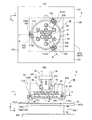
図5(A)は図1中のマーク検出装置8の機構部を示す平面図、図5(B)は図5(A)のBB線に沿う断面図である。なお、図5(A)は、図5(B)のAA線に沿う断面図でもある。マーク検出装置8の機構部は、上述の露光部の他に、ウエハ受け渡し装置66、マーク検出部52、及びエッジ検出部53A,53Bを備えている。図5(B)において、ウエハ受け渡し装置66は、円板状の本体部67と、本体部67の上面に固定されるとともに、フレーム部材FR1に形成された開口内にZ方向に移動可能に配置された円柱状のスライド部材69と、スライド部材69の上端に固定されたフランジ部69Fと、フレーム部材FR1に対してフランジ部69FのZ方向の位置を制御する複数のアクチュエータ70と、を有する。アクチュエータ70としては、例えば直動型のねじ機構、又はエアーシリンダ等が使用可能であり、フランジ部69FのZ位置を計測するセンサ(不図示)も装着されている。図3の搬送制御系50がそのセンサの計測値に基づいてアクチュエータ70を駆動することで、フランジ部69Fにスライド部材69を介して連結された本体部67のZ位置を制御できる。なお、本体部67のZ位置を制御する機構としては、アクチュエータ70を用いる機構以外の任意の機構を使用できる。
Next, the configuration and operation of the
5A is a plan view showing a mechanism part of the
また、本体部67はウエハWよりもわずかに大きい円形である。そして、ウエハ受け渡し装置66は、本体部67の底面に固定された複数の短い円柱状の非接触の吸引装置(以下、サクションカップという。)68と、本体部67の側面にほぼ等角度間隔(ここでは120度間隔)で固定された連結部材71A,71B,71C(図5(A)参照)と、連結部材71A,71B,71Cに対して回転用のモータ71Am,71Bm等によって回転可能に取り付けられたL字形の吸着部72A,72B,72Cとを備えている。サクションカップ68は、ベルヌーイカップ又はベルヌーイチャックと呼ぶこともできる。吸着部72A〜72Cの先端部は、代表的に点線の位置B5で示すように、それぞれ対応するモータ71Am等によって本体部67の側面方向に退避可能である。さらに、吸着部72A〜72Cの先端部は、それぞれ対応するモータ71Am等によって本体部67の底面と平行になるまで回転可能であり、この状態で吸着部72A〜72Cの先端部にウエハWを支持可能である。吸着部72A〜72Cの先端部には真空吸着用の穴(不図示)が設けられ、この穴から可撓性を持つ配管(不図示)を介して真空ポンプ(不図示)で気体を吸引することで、ウエハWを吸着保持できる。
The
図5(B)は、本体部67の底面の複数のサクションカップ68に所定間隔を隔てて対向するように、吸着部72A〜72Cの先端部でウエハWを保持している状態を示す。図5(A)に示すように、複数のサクションカップ68は、一例としてウエハWの表面の中心及び複数の同心円状に配置された位置に対向するように配置されている。なお、図5(A)において、本体部67は2点鎖線で表されている。
FIG. 5B shows a state in which the wafer W is held by the tip portions of the
サクションカップ68は、矢印B1で示すように、それぞれほぼウエハWに対向する面に沿って放射状に可変の流量で清浄な気体を噴き出しており、その面とウエハWとの距離が大きくなると、ベルヌーイ効果による負圧が発生してウエハWがサクションカップ68側に吸引され、その面とウエハWとの距離が小さくなると、圧力エアクッション効果によってウエハWをサクションカップ68から離す力が作用する。この結果、サクションカップ68とウエハWとの距離を、非接触でその気体の流量に応じた値に維持できる。そして、搬送制御系50が、複数のサクションカップ68とウエハWとの距離を互いに独立に制御することで、実質的に非接触に保持しているウエハWの形状を例えばウエハステージWST側に凸となる形状(以下、下凸形状という)を含む任意の形状に設定できる。例えば複数のサクションカップ68によってウエハWを下凸形状にして非接触に保持し、ウエハWの下方にウエハステージWSTのウエハホルダ44を移動し、吸着部72A〜72Cの先端部を本体部67の側面方向に退避させて、アクチュエータ70を駆動して本体部67をウエハホルダ44側に降下させることで、大型のウエハWを変形させることなくウエハホルダ44の上面に載置することができ、ウエハWの残留歪みの発生を防止できる。
As indicated by an arrow B1, the
また、マーク検出部52は、連結部材71A(吸着部72A)の近傍で本体部67に固定された第1光学系54Aと、吸着部72Aに装着された第2光学系54Bと、を有する。また、エッジ検出部53A及び53Bは、それぞれ連結部材71B及び71Cの近傍で本体部67に固定されている。なお、マーク検出部52の第1光学系54A及びエッジ検出部53A,53Bは、フレーム部材FR1に固定してもよい。
Further, the
図6(A)は、図5(B)中のマーク検出部52を示す。図6(A)において、ウエハWはウエハ受け渡し装置66の吸着部72A(不図示)の先端部に保持され、ウエハWの裏面にマーク46が形成されている。また、マーク検出部52の第1光学系54Aは、ウエハWのフォトレジストに対する感光性の低い波長域である例えば可視域の検出用の光(以下、検出光という)をほぼ−Z方向に射出する光源73を有する。一例として、光源73は発光ダイオード(LED)であるが、光源73として、ランプとライトガイドとの組み合わせ等も使用できる。光源73から射出される検出光のうち、ウエハWのエッジ部の検出に使用される第1検出光DL1を点線で表し、ウエハWの裏面のマーク46の検出に使用される第2検出光DL2を実線で表している。なお、後述するウエハW上面に形成される膜材料等の回り込みによるマーク46が汚染されている可能性を考慮して、少なくとも第2検出光DL2は波長帯域が広い光(ブロードバンドな検出光)を用いることが好ましい。
FIG. 6A shows the
第1光学系54Aは、光源73から射出された検出光DL1,DL2をそれぞれ集光及びコリメートする照明用の第1レンズ系74A及び第2レンズ系74Bと、そのコリメートされた検出光DL1,DL2をほぼ−Y方向に反射するミラーM1と、ミラーM1で反射された検出光DL1,DL2の一部をほぼ−Z方向のウエハW側に向かう検出光DL1,DL2として分岐するハーフプリズム76と、分岐された検出光DL1,DL2を集光する第1対物レンズ系77Aと、を有する。さらに、第1光学系54Aは、第1対物レンズ系77Aとともに結像光学系を形成する第2対物レンズ77Bと、CCD型又はCMOS型等の2次元の撮像素子79と、撮像素子79の受光面の一部の領域の前面に配置されて第2検出光DL2の光路長を補正する光路長補正用ガラス板80と、ミラーM1とハーフプリズム76との間に配置された照明用の開口絞り(以下、照明σ絞りという)75Aと、ハーフプリズム76と第2対物レンズ系77Bとの間に配置された結像用の開口絞り75Bと、を有する。第1光学系54Aは鏡筒部材(不図示)に支持されている。
The first
一例として、ウエハWのエッジ部は被検領域(視野)の中心部にあり、ウエハWの裏面のマーク46は被検領域の周辺部にあるため、照明σ絞り75A内で第1検出光DL1はほぼ光軸に平行であり、第2検出光DL2は光軸に対して比較的大きく傾斜している。また、ウエハ受け渡し装置66の吸着部72A(図6(A)では不図示)内にウエハWの裏面のマーク46に対向するように、マーク検出部52の第2光学系54Bとしての直角プリズム形の光学部材82が設けられている。一例として、光学部材82は、ウエハWの裏面に平行な入射面と、この入射面に45度で交差するとともに互いに直交する2つの反射面とを有する。
As an example, since the edge portion of the wafer W is at the center of the test region (field of view) and the
図6(B)の部分拡大図で示すように、光学部材82の入射面は、ウエハWのエッジ部及びこの近傍の領域に対向する部分が反射面82bとなり、反射面82bにY方向に接する部分(マーク46に対向する部分を含む)が透過面82a,82c(図6(C)参照)となっている。図6(C)は図6(B)内の光学部材82の平面図である。図6(C)に示すように、光学部材82の入射面の透過面82cにX方向に隣接する部分が反射面82d,82eとなり、反射面82d,82e中にY方向に細長いライン状の指標マーク83A,83Bが形成されている。一例として、指標マーク83A,83Bは反射面82d,82eの他の領域よりも反射率が低い領域(黒色部)であるが、指標マーク83A,83Bを他の領域よりも反射率が高い領域としてもよい。
As shown in the partial enlarged view of FIG. 6B, on the incident surface of the
マーク検出部52において、第1対物レンズ系77Aから射出された第1検出光DL1は光学部材82の反射面82b(図6(B)参照)に入射する。その反射面82bで反射された第1検出光DL1は、ウエハWのエッジ部の外側を通過し、第1対物レンズ系77A、ハーフプリズム76A、及び第2対物レンズ系77Bを介して、撮像素子79の受光面の中央部にウエハWのエッジ部の像を形成する。
In the
一方、第1対物レンズ系77Aから射出された第2検出光DL2は、光学部材82の透過面82a、光学部材82の直交する2つの反射面、及び光学部材82の透過面82c(図6(C)参照)を介して、ウエハWの裏面のマーク46を含む被検領域に入射する。さらに、光学部材82の直交する2つの反射面で反射された第2検出光DL2の一部は、図6(C)の透過面82cを挟むように設けられた2つの指標マーク83A,83Bを照明する。マーク46を含む被検領域で反射されて光学部材82の透過面82cを通過した光束、及び指標マーク83A,83Bを含む領域で反射された光束を含む第2検出光DL2は、光学部材82の直交する2つの反射面、及び光学部材82の透過面82aを介して第1対物レンズ系77Aに戻される。第1対物レンズ系77Aに戻された第2検出光DL2は、ハーフプリズム76A、第2対物レンズ系77B、及び光路長補正用ガラス板80を介して、撮像素子79の受光面の周辺部に、ウエハWのマーク46の像及び指標マーク83A,83Bの像を形成する。
On the other hand, the second detection light DL2 emitted from the first
本実施形態では、図5(A)の吸着部72A〜72CによりウエハWを保持した状態で、図6(A)のマーク検出部52において、対物レンズ系77A,77Bよりなる結像光学系に関して、ウエハWの表面と撮像素子79の受光面とは光学的に共役である。また、その結像光学系、光学部材82、及び光路長補正用ガラス板80に関して、ウエハWの裏面(マーク46が形成されている面)と撮像素子79の受光面とは光学的に共役である。このため、撮像素子79の受光面にはウエハWのエッジ部の像及び裏面のマーク46の像がそれぞれ高いコントラストで形成される。撮像素子79がそれらの像を撮像して得られる検出信号(ここでは撮像信号)は、図3の演算部55に供給される。演算部55でその検出信号を処理することでマーク46及びマーク46の近傍のウエハWのエッジ部の位置情報が求められる。
In the present embodiment, the imaging optical system including the
また、図5(A)のエッジ検出部53A,53Bは、それぞれ図6(A)のマーク検出部52の第1光学系54Aと同様の構成である。エッジ検出部53A及び53Bは、それぞれ対応する被検領域FVA2,FVA1内のウエハWのエッジ部の像を撮像し、得られる検出信号(撮像信号)を演算部55に供給する。演算部55においてその検出信号を処理することで、対応するエッジ部の位置情報を求めることができる。
Also, the
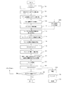
次に、本実施形態の露光装置EXにおいて、マーク検出装置8を用いてウエハWの裏面のマーク46の位置情報等を検出する検出方法、及びこの検出方法を用いる露光方法の一例につき図7のフローチャートを参照して説明する。この方法の動作は主制御装置20及び搬送制御系50によって制御される。まず、図7のステップ102において、図1のレチクルステージRSTにレチクルRがロードされ、レチクルRのアライメントが行われる。この際に、補助レチクルRAのアライメントは予め行われている。その後、不図示のコータ・デベロッパからウエハ搬送ロボットWLDの搬送アーム61に、フォトレジストが塗布されたウエハWが受け渡され、ウエハWを保持した搬送アーム61の先端部が、図8(A)に示すように、ウエハ受け渡し装置66の複数のサクションカップ68の下方に移動する(ステップ104)。なお、図8(B)は、図8(A)のBB線に沿う断面図であり、図8(A)は図8(B)のAA線に沿う断面図に相当する。
Next, in the exposure apparatus EX of the present embodiment, a detection method for detecting position information and the like of the
この際に、本体部67に装着された3つの吸着部72A〜72Cは、代表的に図8(B)の点線の位置B4,B5で示すように、Y方向に移動するウエハWと衝突しない位置に退避している。搬送アーム61の2本のアーム部61a,61bの間には、吸着部72Aが通過できるだけの隙間が確保されている。その後、図8(B)に実線で示すように、吸着部72A〜72Cを回転させて、吸着部72A〜72Cの先端部でウエハWを保持し、ウエハ受け渡し装置66の本体部67をわずかに+Z方向に上昇させることによって、搬送アーム61からウエハ受け渡し装置66にウエハWが受け渡される(ステップ106)。この動作とほぼ並行して、ウエハステージWSTは、ウエハ受け渡し装置66の下方のウエハのローディング位置LPに移動する。そして、搬送アーム61は、矢印B8で示すように−Y方向に移動する。
At this time, the three
その後、図5(A)、(B)に示すように、マーク検出部52の第1光学系54Aから検出光DL1,DL2をウエハWのエッジ部を含む被検領域に照射し、吸着部72A内の第2光学系54B(図6(B)の光学部材82)で反射される第1検出光DL1によって、第1光学系54A内の撮像素子79(図6(A)参照)の受光面にそのエッジ部の像を形成する。これと同時に、ウエハWの裏面で反射される第2検出光DL2及び図6(C)の指標マーク83A,83Bを含む領域で反射される第2検出光DL2を第2光学系54Bを介して受光し、撮像素子79の受光面にウエハWの裏面のマーク46及び指標マーク83A,83Bの像を形成する。撮像素子79の検出信号は演算部55に供給される。
Thereafter, as shown in FIGS. 5A and 5B, the detection regions DL1 and DL2 are irradiated from the first
演算部55ではその検出信号を処理して、一例として、指標マーク83A,83Bを基準として、ウエハWのエッジ部のX方向、Y方向の位置を含む第1の位置情報、並びにマーク46の中心のX方向、Y方向の位置、及びマーク46の回転角を含む第2の位置情報を求める(ステップ108)。一例として、指標マーク83A,83Bに平行な方向の、ステージ座標系(X,Y,Z)のY軸に対する角度(傾斜角)は既知である。そこで、ウエハ裏面のマーク46の回転角として、例えばステージ座標系(X,Y,Z)のY軸に対する傾斜角が求められる。なお、指標マーク83A,83Bを使用することなく、例えば撮像素子79内の所定の位置の一つ又は複数の画素(例えば中心及び周辺の4箇所の画素)を基準としてその第1及び第2の位置情報を求めてもよい。
The
また、ステップ108と実質的に並行に、エッジ検出部53A,53BからウエハWのエッジ部を含む被検領域FVA2,FVA1内に検出光を照射し、2箇所のエッジ部の像を撮像して得られる検出信号を演算部55に供給する。演算部55は、その検出信号から対応する2つのエッジ部の像のX方向、Y方向の位置を含む第3の位置情報を求める(ステップ110)。さらに、演算部55は、そのウエハWの3つのエッジ部の像の位置、及びマーク46の像の回転角より、ウエハWの中心のステージ座標系におけるX方向、Y方向の位置、及びマーク46(ひいてはウエハW自体)のステージ座標系のY軸に対する回転角を算出し、算出結果を記憶部56に記憶するとともに、主制御装置20に供給する(ステップ112)。
Further, in parallel with
そして、図5(B)の状態からウエハ受け渡し装置66の複数のサクションカップ68でウエハWを下凸形状となるように非接触で保持した状態で、ウエハ受け渡し装置66の本体部67を−Z方向に降下させながら、吸着部72A〜72Cを外側に退避させる。さらに、本体部67とともにウエハWを降下させて、ウエハWの中央部がウエハステージWSTのウエハホルダ44の表面に接触したときに、ウエハホルダ44側の真空吸着を開始し、複数のサクションカップ68の保持を解除することで、ウエハWの裏面の全面がウエハホルダ44に載置され、吸着される(ステップ114)。この際に、ステップ112で求められたウエハWの中心位置がウエハホルダ44の中心に来るように、ウエハステージWSTのX方向、Y方向の位置を補正しておいてもよい。この場合には、この補正をウエハWの位置の補正とみなすこともできる。その後、ウエハ受け渡し装置66の本体部67は上昇する。
Then, in the state where the wafer W is held in a non-contact manner by the plurality of
そして、主制御装置20は、一例として、ステージ駆動系18を介して、ステップ112で求められたマーク46(ウエハW)の回転角が既知の目標値になるようにウエハステージWST(又はウエハホルダ44が固定された部分)の回転角を補正し、ステップ112で求められたウエハWの中心位置が目標位置に来るようにウエハステージWSTをX方向、Y方向に移動する(ステップ116)。これによって、ウエハWのプリアライメントが行われたことになる。プリアライメントを行うことによって、ウエハWの1層目のレイヤに露光する場合には、ウエハWの多数のショット領域SAの配列方向が、例えばウエハWのマーク46で規定される方向に応じて設定される。さらに、ウエハWの2層目以降のレイヤに露光する場合には、プリアライメントが行われているため、ウエハWの表面の検出対象のショット領域SAに付設されたウエハマークを迅速にアライメント系ALの被検領域(視野)内に追い込むことができ、ウエハWの最終的なアライメント(ファイン・アライメント)を効率的に行うことができる。
Then, as an example,
その後、ウエハステージWSTを駆動してウエハWを投影光学系PLの下方(露光位置)に移動する過程で、アライメント系ALを用いてウエハWのアライメントが行われる(ステップ118)。そして、図1のレチクルステージRSTを駆動して、補助レチクルRAの代替マーク用パターン21を照明系ILSの照明領域IAR内の中央に移動し、照明系ILS内のレチクルブラインドを用いて、代替マーク用パターン21を含む狭い領域にのみ照明光ILが照射されるように照明領域を制限する。さらに、ウエハステージWSTを駆動して、図9(A)に示すように、例えばマーク検出部52の被検領域FVBとなっていた領域内のウエハWの表面のエッジ部Wfに近い領域26Aの一部を、図1の投影光学系PLの露光領域IA内に移動する。その領域26Aは、完全なショット領域SAが形成されない領域(いわゆる欠けショットとなる領域)であり、かつデバイス用のレチクルRのパターンの像が露光されないウエハWの周辺領域である。
Thereafter, in the process of driving wafer stage WST to move wafer W below projection optical system PL (exposure position), alignment of wafer W is performed using alignment system AL (step 118). Then, the reticle stage RST of FIG. 1 is driven, the
そして、図9(B)に示すように、ウエハWの裏面のマーク46に対向するウエハWの表面Waの領域26A内に、補助レチクルRAの代替マーク用パターン21の像(代替マーク像)21APを露光する(ステップ120)。なお、この代替マーク用パターン21は、後述のとおりウエハWの裏面のマーク46との位置関係が予め考慮されて露光される。このとき主制御装置20は、マーク46と代替マーク用パターン21との位置関係を記憶しておいてもよし、露光装置EXの主制御装置20がアクセス可能な外部のデータベースに保存されていてもよい。
Then, as shown in FIG. 9B, an image (substitute mark image) 21AP of the
一例として、ウエハWのフォトレジストがポジ型である場合、像21APは、Y方向に配列された複数(ここでは3本)の光量の大きいラインパターン部と、X方向に配列された複数(ここでは3本)の光量の大きいラインパターン部とから構成されている。なお、図9(B)及び(C)内の代替マーク用パターン21の像21AP,21CPは、ショット領域SAに対して相対的に大きく表されている。また、代替マーク用パターン21は、デバイス用パターンのうちの最も微細なパターンと比べると線幅が広いため、代替マーク用パターン21の像は液浸方式を使用することなく、ドライ方式で露光してもよい。
As an example, when the photoresist of the wafer W is a positive type, the image 21AP includes a plurality (three in this case) of line patterns having a large amount of light arranged in the Y direction and a plurality of (here here) arranged in the X direction. 3 lines) having a large amount of light. It should be noted that the images 21AP and 21CP of the
さらに、ウエハステージWSTを駆動して、図9(A)に示すように、エッジ検出部53A及び53Bの被検領域FVA2,FVA1となっていた領域内のウエハWの表面のエッジ部Wfに近い領域26C及び26Bの一部を、順次、投影光学系PLの露光領域IA内に移動し、それぞれ代替マーク用パターン21の像21CP及び21BPを露光する。領域26C及び26Bも図9(C)に示すようにレチクルRのパターンの像が露光されないウエハWの周辺領域にある。
Further, wafer stage WST is driven, and as shown in FIG. 9A, the
これらの像21AP〜21CPの露光時のウエハステージWSTのステージ座標系における位置情報が演算部55に供給されている。演算部55では、像21AP〜21CPを露光したときのウエハステージWSTの位置情報から、像21AP〜21CPの各中心のX方向、Y方向の位置に基づいて算出されるウエハWの中心位置及び回転角(例えば像21BP,21CPの中心を結ぶ直線に直交する方向の、ステージ座標系のY軸に対する角度)を算出する。そして、この算出結果の、ステップ112で算出され、かつステップ116で補正された後のウエハWの中心位置及び回転角(ここでは0度)に対するオフセット(δx,δy)及びδθを求め、これらのオフセット(δx,δy)及びδθを記憶部56に記憶する(ステップ122)。その傾斜角のオフセットδθは、ウエハWの裏面のマーク46の方向に対する、像21AP〜21CP(ひいては後述の代替マーク21AM〜21CM)の各中心から求められるウエハWの回転角のオフセット角(相対角度)と言うことができる。
Position information in the stage coordinate system of wafer stage WST at the time of exposure of these images 21AP to 21CP is supplied to
その後、例えばステップ118のアライメントの結果を用いてウエハWを駆動することで、ウエハWの各ショット領域にレチクルRのパターンの像が走査露光される(ステップ124)。その後、ウエハステージWSTをアンローディング位置UPに移動し、例えば別のウエハ受け渡し装置を降下させ、ウエハホルダ44からそのウエハ受け渡し装置にウエハWを受け渡すことで、ウエハWがアンロードされる(ステップ126)。アンロードされたウエハWはコータ・デベロッパ(不図示)に搬送されて現像され(ステップ130)、その後、例えばエッチング工程(ステップ132)を経て次のレイヤのパターン形成工程(ステップ134)に移行する。また、露光装置EXにおいて、次のウエハに露光する場合には(ステップ128)、次のウエハに対してステップ104〜126の動作が繰り返される。
Thereafter, for example, by driving the wafer W using the alignment result in
そのステップ132を経たウエハWの表面には、図9(A)に示すように、マーク検出部52の被検領域FVB、及びエッジ検出部53A,53Bの被検領域FVA2,FVA1となる領域に、それぞれ2次元の代替マーク21AM,21CM,21BMが形成されている。代替マーク21AM等は、それぞれ代替マーク用パターン21の像21AP等の光量の大きい部分が凹部となった凹凸マークである。その後、代替マーク21AM,21CM,21BMが形成されたウエハWの次のレイヤに露光を行う場合には、適宜、代替マーク21AM、21CM、21BMを用いたマーク検出が行われる。例えばウエハWの表面に対する露光動作が繰り返されると、ウエハWの裏面にレジスト材料などの膜材料(異物)が回り込むことがある。そして回り込んだ膜材料が異物としてウエハWの裏面のマーク46に付着した場合、マーク検出部52によるマーク46の検出が困難となってしまう可能性がある。また、ウエハWの露光処理などにおいて、マーク46が何らかの原因(磨耗など)でマーク検出部52によるマーク46の検出が困難になる場合も考えられる。
As shown in FIG. 9A, on the surface of the wafer W that has undergone
上記のような場合には、図7のステップ108,110の代わりに、ステップ108Aの動作が実行される。
このステップ108Aにおいて、図5(B)に示すように、ウエハ受け渡し装置66の吸着部72A〜72CによってウエハWが保持されている状態で、マーク検出部52の第1光学系54Aからの第1検出光DL1がウエハWのエッジ部に照射される。そして、図6(A)の光学部材82で反射された第1検出光DL1、及び図9(A)のウエハWの表面の代替マーク21AMを含む部分で反射された第1検出光DL1が、図5(B)の第1光学系54Aに戻され、第1光学系54A内の撮像素子79(図6(A)参照)によってウエハWのエッジ部及び代替マーク21AMの像が撮像され、この検出信号が演算部55に供給される。なお、このステップ108Aでは、ウエハWのエッジ部の像は必ずしも必要ではない。また、撮像素子79の受光面の周辺部には、ウエハWの裏面のマーク46の不鮮明な像が形成される可能性もあるが、その不鮮明な像は使用されない。
In the above case, the operation of
In this
この代替マーク21AMの像の撮像と並行して、図5(A)のエッジ検出部53A,53Bによって図9(A)のウエハWの表面の代替マーク21CM,21BMの像が撮像され、この検出信号が演算部55に供給される。演算部55では、図7のステップ112に対応する工程で、それらの検出信号を処理して、代替マーク21AM,21BM,21CMの中心位置に基づいてウエハWの中心位置及びウエハWの回転角(例えば代替マーク21BM,21CMの中心を結ぶ直線に直交する方向の、ステージ座標系のY軸に対する角度)を算出する。さらに、演算部55は、例えばこれらの算出結果からステップ122で記憶した位置及び回転角のオフセット(δx,δy)及びδθを差し引いてウエハWの中心位置及び回転角を求め、求めた結果を記憶部56に記憶する。
In parallel with the image pickup of the substitute mark 21AM, the
その後、ステップ116でウエハWの中心及び回転角を補正することで、ウエハWの中心位置及び回転角は、マーク検出部52によって検出されるウエハWの裏面のマーク46及びウエハWのエッジ部の位置と、エッジ検出部53A,53Bによって検出されるウエハWの2箇所のエッジ部の位置とから求められる結果に基づいて設定された場合と同じ位置及び回転角に設定される。
Thereafter, the center position and rotation angle of the wafer W are corrected in
この露光方法によれば、ウエハWの外形に切り欠き部がなく、ウエハWの裏面にマーク46が形成されている場合に、マーク検出装置8によってマーク46及びウエハWの3箇所のエッジ部の位置情報を検出し、この検出結果からウエハWの中心位置及びマーク46(ウエハW)の回転角を求めることで、ウエハWのプリアライメントを行うことができる。従って、ウエハWの2層目以降に露光する場合には、ウエハWの最終的なアライメントを効率的に行うことができ、レチクルRのパターンの像を高い重ね合わせ精度でウエハWの各ショット領域に露光できる。また、ウエハWの2層目以降に露光する場合に、ウエハWの裏面のマーク46の検出が困難となっていても、ウエハWの表面に形成した代替マーク21AM〜21CMに基づいてウエハWの中心及び回転角を正確に検出でき、この検出結果に基づいてウエハWのプリアライメントを正確に行うことができる。
According to this exposure method, when there is no notch on the outer shape of the wafer W and the
なお、図4(F)に示すように、直径が300mm等であって、切り欠き部としてノッチ部NTが設けられている従来のウエハW1を使用する場合、例えば2つの被検領域(視野)FVA1,FVA2でウエハW1のエッジ部の位置が検出され、被検領域FVA3でノッチ部NTの位置及び方向が検出され、これらの検出結果からウエハW1の中心及び回転角が求められていた。一方、図4(G)に示すように、直径が300mm等であって、切り欠き部としてオリエンテーションフラット部OFが設けられているウエハW2を使用する場合、例えば2つの被検領域FVA2,FVA3でオリエンテーションフラット部OFの位置及び角度が検出され、被検領域FVA1でウエハW2のエッジ部の位置が検出され、これらの検出結果からウエハW2の中心及び回転角が求められていた。そして、このようにして求められたウエハW1,W2の中心及び回転角に基づいてウエハW1,W2のプリアライメントが行われていた。 As shown in FIG. 4F, when a conventional wafer W1 having a diameter of 300 mm or the like and provided with a notch portion NT as a notch portion is used, for example, two test regions (fields of view) are used. The position of the edge portion of the wafer W1 is detected by the FVA1 and FVA2, the position and direction of the notch portion NT is detected in the test region FVA3, and the center and rotation angle of the wafer W1 are obtained from these detection results. On the other hand, as shown in FIG. 4G, when using a wafer W2 having a diameter of 300 mm or the like and provided with an orientation flat portion OF as a notch, for example, in two test regions FVA2 and FVA3 The position and angle of the orientation flat portion OF are detected, the position of the edge portion of the wafer W2 is detected in the test area FVA1, and the center and rotation angle of the wafer W2 are obtained from these detection results. Based on the centers and rotation angles of the wafers W1 and W2 thus obtained, the wafers W1 and W2 are pre-aligned.
これに対して、本実施形態のように外形に切り欠き部がなく、裏面にマーク46が形成されたウエハWを使用する場合には、マーク検出装置8を用いてそのウエハ裏面のマーク46の位置情報を検出することによって、ウエハWのプリアライメントを行うことができる。
また、本実施形態の露光装置によれば、ウエハ受け渡し装置66を用いてウエハWを実質的に非接触状態で下凸形状にして、ウエハWをウエハステージWSTのウエハホルダ44に載置している。このため、ウエハWが450mmウエハのように大型であっても、ウエハWの残留歪み等がない状態で、ウエハWの平面度を高く維持した状態で、ウエハWをウエハホルダ44に保持できる。従って、大型のウエハWを用いて高いスループットを得るとともに、ウエハWの全面で露光精度(解像度等)を高く維持して、レチクルRのパターンの像を高精度に露光できる。
On the other hand, when using a wafer W having no cutout in the outer shape and having the
Further, according to the exposure apparatus of the present embodiment, the wafer W is placed in the downward convex shape in a substantially non-contact state using the
上述のように本実施形態の露光装置EXは、ウエハW(基板)に形成されたマークの位置情報(角度情報を含む)を検出するマーク検出装置8を備えている。そして、マーク検出装置8は、裏面にマーク46(第1マーク)が形成されたウエハWを一時的に保持するウエハ受け渡し装置66(基板保持部)と、ウエハ受け渡し装置66にウエハWが保持されている状態で、マーク46の位置情報を検出するマーク検出部52(第1検出部)と、検出されたマーク46の位置情報に基づいて、ウエハWの表面に代替マーク21AM〜21CM(第2マーク)を形成するための像21AP〜21CMを露光する露光部(照明系ILS、補助レチクルRAを備えるレチクルステージRST、及び投影光学系PL)を含むマーク形成部と、を備えている。さらに、マーク検出装置8は、マーク46と代替マーク21AM〜21CMとの位置関係(例えばマーク46の方向に対する、代替マーク21AM〜21CMの各中心から求められるウエハWの回転角のオフセット)を記憶する記憶部56と、ウエハ受け渡し装置66にウエハWが保持されている状態で、代替マーク21AM〜21CMの位置情報を検出するマーク検出部52及びエッジ検出部53A,53B(第2検出部)と、を備えている。
As described above, the exposure apparatus EX of the present embodiment includes the
また、本実施形態のウエハWのマークの位置情報を検出するマーク検出方法は、裏面にマーク46が形成されたウエハWをウエハ受け渡し装置66で一時的に保持するステップ106と、ウエハ受け渡し装置66にウエハWが保持されている状態で、マーク46の位置情報を検出するステップ108と、を有する。さらに、そのマーク検出方法は、検出されたマーク46の位置情報に基づいて、ウエハWの表面に代替マーク21AM〜21CMを形成するステップ120,130,132と、マーク46と代替マーク21AM〜21CMとの位置関係を記憶するステップ122と、ウエハ受け渡し装置66にウエハWが保持されている状態で、代替マーク21AM〜21CMの位置情報を検出するステップ108Aと、を有する。
The mark detection method for detecting the position information of the mark on the wafer W according to the present embodiment includes a
本実施形態によれば、ウエハ受け渡し装置66にウエハWが保持されている状態で、ウエハWの裏面のマーク46の位置情報を検出している。すなわち、ウエハWをウエハステージWSTに載置するまでの搬送中にマーク46を検出しているため、ウエハWが450mmウエハのように大型で、かつ裏面にマーク46が形成されている場合であっても、マーク46の位置情報を効率的に検出できる。さらに、ウエハWの表面に形成される代替マーク21AM〜21CMと、ウエハWの裏面のマーク46との位置関係を記憶しているため、マーク46の検出が困難になった場合でも、代替マーク21AM〜21CMの位置情報を検出することによって、この検出結果に基づいて、ウエハWの裏面のマーク46の位置情報を検出した場合と同様に、ウエハWの回転角を含む位置情報を検出できる。
According to the present embodiment, the position information of the
また、本実施形態の露光装置EXは、露光用の照明光ILでレチクルRのパターンを照明し、照明光ILでそのパターンを介してウエハWを露光する露光装置であって、マーク検出装置8と、マーク検出装置8によって検出されるウエハWの裏面のマーク46又はウエハWの表面の代替マーク21AM〜21CMの位置情報に基づいて、ウエハWの中心の位置及び回転角を補正する主制御装置20(制御部)と、を備えている。そして、露光装置EXによる露光方法は、本実施形態のマーク検出方法を用いてウエハWのマーク46又は代替マーク21AM〜21CMの位置情報を検出するステップ108,108Aと、ウエハWをウエハステージWSTに載置するステップ114と、そのマーク検出方法によって検出された位置情報に基づいて、ウエハWの中心の位置及び回転角を補正するステップ116と、を有する。
The exposure apparatus EX of the present embodiment is an exposure apparatus that illuminates the pattern of the reticle R with the illumination light IL for exposure and exposes the wafer W through the pattern with the illumination light IL. And the main controller for correcting the position and rotation angle of the center of the wafer W based on the position information of the
本実施形態の露光装置又は露光方法によれば、大型のウエハWを使用することによって高いスループットを得ることができる。さらに、ウエハWの裏面にマーク46が形成されていても、さらにマーク46の検出が困難であっても、そのマーク46又は代替マーク21AM〜21CMの位置情報を効率的に検出でき、この検出結果を用いてウエハWの位置及び回転角を補正することでプリアライメントが行われる。このため、その後のウエハWの最終的なアライメントを効率的に行うことができ、より高いスループットを得ることができる。
According to the exposure apparatus or the exposure method of this embodiment, high throughput can be obtained by using a large wafer W. Further, even if the
なお、上記の実施形態では以下のような変形が可能である。
まず、上記の実施形態では、ステップ116でウエハWの中心の位置及び回転角を補正しているが、その位置及び回転角の少なくとも一方を補正するだけでもよい。
また、上記の実施形態では、ウエハWは一例として450mmウエハであるが、例えば300mmウエハ、又は他の任意の大きさのウエハにおいても、切り欠き部を設ける代わりに裏面にマークを設けるような場合には、上記の実施形態のマーク検出装置8と同様の検出装置又は検出方法を用いてそのウエハの裏面のマークを検出し、この検出結果に基づいてそのウエハWの表面に代替マークを形成しても良い。
In the above embodiment, the following modifications are possible.
First, in the above-described embodiment, the position and rotation angle of the center of the wafer W are corrected in
In the above embodiment, the wafer W is a 450 mm wafer as an example. However, for example, even in a 300 mm wafer or other arbitrary size wafer, a mark is provided on the back surface instead of providing a notch. First, a mark on the back surface of the wafer is detected using a detection device or detection method similar to the
また、上記の実施形態では、ウエハWの裏面のマーク46の代替マークとして、図9(B)のような2次元の代替マーク21AM等が使用されているが、その代替マークの形状は任意である。例えば、その代替マークとして、図9(D)に示すように、枠状の凹部(又は凸部でもよい、以下同様)よりなる中心部27Aaと、この中心部27AaをX方向及びY方向に挟むようにそれぞれ配置された複数の凹部よりなるラインパターンと、を含む2次元のマーク27Aを使用できる。さらに、その代替マークとして、図9(E)に示すように、X方向に細長い凹部よりなる複数のラインパターン27BYと、ラインパターン27BYをX方向に挟むように配置された複数のY方向に細長い凹部よりなるラインパターン27BXと、を含む2次元のマーク27Bを使用できる。
In the above embodiment, a two-dimensional substitute mark 21AM as shown in FIG. 9B is used as a substitute mark for the
また、ウエハWの裏面のマーク46の代替マークとして、図9(F)に示すように、図4(B)のマーク46と同様に、Y方向(ウエハWの中心に対して半径方向)に複数の小さい凹部27Caを形成した代替マーク27Cを使用することもできる。この代替マーク27Cは、図4(B)のマーク46と同様に、複数の凹部27Caの中心を通る直線の方向をこの代替マーク27Cの方向とみなすことができる。代替マーク27Cを使用するとき、マーク46と代替マーク27Cとの位置関係として、マーク46の方向と代替マーク27Cの方向との間の角度(相対角度)を記憶してもよい。
Further, as a substitute mark for the
また、上記の実施形態では、代替マーク21AP等はウエハWの表面のエッジ部Wfに近い周辺領域に形成されているが、図9(B)又は(C)に示すように、ウエハWの表面の隣接する複数のショット領域SA間のスクライブライン領域SL内に、代替マーク21AP等を形成してもよい。なお、代替マーク21AP等は、実際にはスクライブライン領域SL内に容易に収まる程度の大きさである。 In the above embodiment, the substitute marks 21AP and the like are formed in a peripheral region near the edge portion Wf on the surface of the wafer W. However, as shown in FIG. An alternative mark 21AP or the like may be formed in the scribe line area SL between a plurality of adjacent shot areas SA. Note that the substitute marks 21AP and the like are actually large enough to fit within the scribe line area SL.
また、上記の実施形態では、ウエハWの裏面のマーク46の代替マークとして、図9(A)に示すように、ウエハWの表面に3個の代替マーク21AM〜21CMを形成している。しかしながら、代替マークは、例えばウエハWの裏面のマーク46に対応させて、ウエハWの表面に一つのみを形成してもよい。このために、一例として、ウエハWの裏面のマーク46に対応させて、ウエハWの表面のマーク検出部52による被検領域内に、図9(F)に示す一つの代替マーク27Cを形成してもよい。この場合、図7のステップ116でウエハWの回転角をウエハWの裏面のマーク46の方向がステージ座標系のY軸に平行になるように補正した後、ステップ120で、代替マーク27Cを形成するための補助レチクル(不図示)のパターンの像(複数のドットパターンの像)の方向をY軸に平行にしてそのパターンの像を露光してもよい。このとき、代替マーク27Cの方向はマーク46の方向に平行になっているため、代替マーク27Cとマーク46との位置関係として、それらのマーク間の相対角度が0度であることが記憶される。従って、この後、ウエハWの裏面のマーク46が検出できない場合には、マーク検出部52によってウエハWの表面の代替マーク27Cを検出し、この代替マーク27Cの方向をウエハWの方向とすることによって、マーク46を検出した場合と同様に、ウエハWの回転角を正確に補正できる。
Further, in the above embodiment, as the substitute marks for the
また、上記の実施形態では、ウエハWの裏面のマーク46の検出結果に基づいてウエハWの表面に代替マークを形成している。しかしながら、ウエハWの表面に代替マークを形成する代わりに、図9(B)に示すように、ウエハWの表面Waのある領域であって、その表面内のパターン(例えばデバイス用の回路パターンDP1)又は反射率分布(例えば基材SUの表面又はあるレイヤの反射率分布)が他の領域のパターン又は反射率分布と識別可能な領域(以下、特徴部という)CPの位置情報を検出してもよい。
Further, in the above embodiment, the substitute mark is formed on the front surface of the wafer W based on the detection result of the
特徴部CPをマーク検出部52で検出する場合、一例として、マーク検出部52の撮像素子79で撮像されるウエハWの表面の像から、ある画素を中心とする部分領域を選択し、この部分領域をX方向及びY方向に1画素ずつ例えば数画素までずらして得られる複数のシフト部分領域を選択する。さらに、一例として、その部分領域と、複数のシフト部分領域との間の複数の画素の検出信号の差分の絶対値の積算値を識別値とする。そして、その部分領域と、その複数のシフト部分領域との間の識別値がそれぞれ予め定めた閾値よりも大きいときに、その部分領域を他の領域と識別可能な特徴部CPの像とみなすことができる。
When the feature CP is detected by the
この場合、演算部55では、そのマーク検出部52からの検出信号を処理して、その特徴部CPの像の画素毎の検出信号の分布を求め、この検出信号の分布を記憶部56に記憶させる。さらに、演算部55では、ウエハWの裏面のマーク46の像の方向と、その特徴部CPの像の方向(例えば特徴部CPの像内のある2つの位置(画素)を通る直線の方向)とがなす角度、及びマーク46の像の中心と特徴部CPの像の中心との位置ずれ量を、マーク46と特徴部CPとの相対位置の情報として求め、この相対位置の情報を補正情報として記憶部56に記憶させる。その後、ウエハWの次のレイヤに露光する場合であって、かつウエハWの裏面のマーク46の検出が困難である場合には、マーク検出部52によって検出されるウエハWのエッジ部を含む被検領域の画像から、特徴部CPの像の検出信号の分布に最も近い検出信号の分布を持つ領域を特徴部CPの像として求める。そして、この特徴部CPの像の位置と方向とを求め、この位置と方向とを上記の記憶してある補正情報で補正することによって、ウエハWの裏面のマーク46の位置及び方向を正確に推定できる。このため、この推定されるマーク46の位置及び方向を用いて、ステップ112でウエハWの中心及び回転角を正確に算出できる。
In this case, the
この特徴部CPを検出する場合のマーク検出装置8は、裏面にマーク46が形成されたウエハWを一時的に保持するウエハ受け渡し装置66と、ウエハ受け渡し装置66にウエハWが保持されている状態で、ウエハWの裏面のマーク46の位置情報を検出するマーク検出部52(第1検出部)と、ウエハWの表面であってこの表面の他の領域内のパターン又は反射率分布と識別可能な特徴部CPの位置情報を検出するマーク検出部52(第2検出部)と、マーク46と特徴部CPとの位置関係(相対角度等)を記憶する記憶部56と、を備えている。
The
なお、本実施形態では、マーク46を検出するマーク検出部52と、特徴部CPを検出するマーク検出部52とは同一であるが、特徴部CPを検出する検出部はマーク検出部52と異なっていてもよい。
また、その特徴部CPを検出する場合のマーク検出方法は、裏面にマーク46が形成されたウエハWをウエハ受け渡し装置66で一時的に保持するステップ106と、ウエハ受け渡し装置66にウエハWが保持されている状態で、マーク46の位置情報を検出するステップ108と、を有する。さらに、そのマーク検出方法は、ウエハWの表面の特徴部CPの位置情報を検出し(ステップ108に対応する工程)、マーク46と特徴部CPとの位置関係を記憶する(ステップ112に対応する工程)。
In this embodiment, the
The mark detection method for detecting the feature portion CP includes a
このように特徴部CPを用いる場合にも、ウエハWが450mmウエハのように大型で、かつ裏面にマーク46が形成されていても、マーク46の位置情報を効率的に検出できる。さらに、ウエハWの表面の特徴部CPと、ウエハWの裏面のマーク46との位置関係を記憶しているため、マーク46の検出が困難になった場合でも、特徴部CPの位置情報を検出することによって、この検出結果に基づいて、ウエハWの裏面のマーク46の位置情報を検出した場合と同様に、ウエハWの回転角を含む位置情報を検出できる。そして、この検出結果に基づいてウエハWのプリアライメントを正確に行うことができる。
As described above, even when the feature portion CP is used, even if the wafer W is large like a 450 mm wafer and the
なお、代替マーク27は、ウエハWの表面に形成される任意の層に設けることができる。例えば実験やシュミレーション等でマーク46の汚染度合いの傾向を把握しておき、この実験やシュミレーション結果に基づく知見から特定の層に代替マーク27を形成しても良い。さらに、上記した実験の結果やシュミレーションの結果を主制御装置20がアクセス可能なデータベースに保存しておき、主制御装置20が適宜アクセスできる状態としてもよい。また、代替マーク27はウエハWの表面の特定の1層だけに形成してもよいし、複数の層に代替マーク27を形成してもよい。
The substitute mark 27 can be provided on any layer formed on the surface of the wafer W. For example, the tendency of the degree of contamination of the
[第2の実施形態]
第2の実施形態につき図10を参照して説明する。本実施形態の露光装置の基本的な構成は図1の露光装置EXとほぼ同様であるが、マーク検出装置の構成、及びウエハステージWSTの位置計測機構の一部の構成が異なっている。なお、図10において、図1、及び図5(A)、(B)に対応する部分には同一又は類似の符号を付してその詳細な説明を省略する。
[Second Embodiment]
A second embodiment will be described with reference to FIG. The basic configuration of the exposure apparatus of the present embodiment is substantially the same as that of the exposure apparatus EX of FIG. 1, but the configuration of the mark detection apparatus and the configuration of a part of the position measurement mechanism of wafer stage WST are different. 10, parts corresponding to those in FIG. 1 and FIGS. 5A and 5B are denoted by the same or similar reference numerals, and detailed description thereof is omitted.
図10は、本実施形態に係るマーク検出装置8Aの機構部を示す。マーク検出装置8Aでは、ウエハWを一時的に保持する基板保持部として、第1の実施形態のウエハ受け渡し装置66の代わりにウエハ搬送ロボットWLDが使用されている。また、ウエハステージWSTのウエハホルダ44中にはZ方向に移動可能に真空吸着可能な複数の棒状部材(センターピン)(不図示)が配置され、これらの棒状部材を介してウエハ搬送ロボットWLDの搬送アーム61からウエハホルダ44にウエハWを受け渡すことができるように構成されている。従って、本実施形態では、図5(A)のウエハ受け渡し装置66は必ずしも必要ではない。
FIG. 10 shows a mechanism part of the
また、図10は、ベース盤WB上のウエハステージWSTが、ウエハ搬送ロボットWLDのウエハWを保持する搬送アーム61の下方のローディング位置LPに向かって−Y方向に移動している状態を示している。本実施形態の露光装置のウエハステージWSTのステージ本体30の底面部には、Y方向に貫通するように開口部30aが形成され、開口部30aの上面に、図2の回折格子12A〜12Dと同様の2次元の回折格子12Eが固定されている。
FIG. 10 shows a state where wafer stage WST on base board WB is moving in the −Y direction toward loading position LP below
また、床面に対して防振装置(不図示)を介して安定にフレーム部材FR2が支持されている。フレーム部材FR2の底面にL字形の分岐フレームFR3が固定されている。ウエハ搬送ロボットWLDの搬送アーム61等は、分岐フレームFR3に設けられた切り欠き部FR3b内を移動可能である。分岐フレームFR3のY方向に平行な細長い平板状のロッド部FR3aの+Y方向側の端部に、図2の検出ヘッド14と同様に、回折格子12Eに計測ビームを照射して回折格子12E(ひいてはウエハステージWST)との間のX方向、Y方向の相対変位を計測する検出ヘッド14Aが固定されている。すなわち、ウエハステージWSTを−Y方向に移動すると、分岐フレームFR3のロッド部FR3aがステージ本体30の開口部30a内に差し込まれ、ロッド部FR3aに設けられた検出ヘッド14Aによってステージ本体30に設けられた回折格子12Eを検出可能となる。このように本実施形態の露光装置は、図3のエンコーダ6に加えて、回折格子12E及び検出ヘッド14Aよりなる付加的なエンコーダを備えている。この付加的なエンコーダによって、ローディング位置LPの近傍でウエハステージWSTのX方向、Y方向の位置を計測できる。
Further, the frame member FR2 is stably supported on the floor surface via a vibration isolator (not shown). An L-shaped branch frame FR3 is fixed to the bottom surface of the frame member FR2. The
また、本実施形態のマーク検出部52Aは、フレーム部材FR2に設けられた第1光学系54Cと、分岐フレームFR3のロッド部FR3aに設けられた第2光学系54Dとを有する。第1光学系54Cは、ウエハWのエッジ部を含む領域に検出光DL1を照射し、そのウエハWからの反射光を受光し、内部の第1の撮像素子79Aによってそのエッジ部の像を撮像する。
The
また、第2光学系54Dにおいて、光源73Aから射出された検出光DL1と同じ波長域の検出光DL2は、照明用のレンズ系74Aを介してハーフプリズム76Aに入射し、ハーフプリズム76Aで+Z方向に分岐された検出光DL2はウエハWの裏面のマーク46を含む被検領域を照明する。この被検領域で反射された検出光DL2は、ハーフプリズム76Aを通過し、ロッド部FR3aに設けられた開口(不図示)を通過し、ロッド部FR3aの底面側でミラーM2により反射される。反射された検出光DL2は、対物レンズ系77C,77D(結像光学系)を介して第2の撮像素子79Bの受光面にウエハWの裏面のマーク46の像を形成する。撮像素子79A,79BはそれぞれウエハWのエッジ部及びマーク46の像を撮像し、検出信号を図3の演算部55に供給する。
In the second
また、フレームFR2に、第1光学系54CとともにウエハWのエッジ部に沿ってほぼ等角度間隔でエッジ検出部53A,53Bと同様の構成のエッジ検出部53A1,53B1が設けられている。エッジ検出部53A1,53B1によってウエハWの2箇所のエッジ部の像が撮像され、検出信号が演算部55に供給される。演算部55ではそれらの検出信号を処理してウエハWの中心の位置及び回転角を求める。その後、ウエハステージWSTを搬送アーム61の下方(ローディング位置LP)に移動して、搬送アーム61からウエハステージWSTのウエハホルダ44にウエハWを受け渡した後、ウエハWの位置及び回転角を補正することでウエハWのプリアライメントが行われる。
The frame FR2 is provided with edge detection units 53A1 and 53B1 having the same configuration as the
また、第1の実施形態と同様に、ウエハWの表面に図9(A)の代替マーク用のパターンの像21AP,21BP,21CPが露光され、現像、及びエッチングによって代替マーク21AM,21BM,21CMが形成される。これらの代替マーク21AM,21BM,21CMの位置情報は、図10のマーク検出部52Aの第1光学系54C、及びエッジ検出部53B1,53A1によって検出することができる。従って、第1の実施形態と同様に、ウエハWの裏面のマーク46の検出が困難であっても、代替マーク21AM,21BM,21CMの位置情報を検出することによって、この検出結果に基づいてウエハWのプリアライメントを行うことができる。
Similarly to the first embodiment, the image 21AP, 21BP, 21CP of the pattern for the substitute mark shown in FIG. 9A is exposed on the surface of the wafer W, and the substitute marks 21AM, 21BM, 21CM are developed and etched. Is formed. Position information of these substitute marks 21AM, 21BM, and 21CM can be detected by the first
なお、上記の各実施形態では、ウエハWのエッジ部を検出するために撮像方式の第1光学系54C、及びエッジ検出部53A,53B等が使用されている。別の構成として、例えばウエハWのエッジ部を通るように平行な光ビームを照射し、そのエッジ部を通過した光を集光光学系を介してフォトマルチプライア又はフォトダイオード等の光電検出器で受光し、この受光量(検出信号)からそのエッジ部の位置を検出してもよい。
また、上記の実施形態では、マーク形成部として補助レチクルのパターンを露光する露光部が使用されているが、マーク形成部としては、例えばレーザパルスを照射してウエハの表面にマークを形成する装置など、他の任意の装置を使用できる。
In each of the above embodiments, the first optical system 54 </ b> C of the imaging method, the edge detectors 53 </ b> A and 53 </ b> B, and the like are used to detect the edge portion of the wafer W. As another configuration, for example, a parallel light beam is irradiated so as to pass through the edge portion of the wafer W, and the light passing through the edge portion is detected by a photoelectric detector such as a photomultiplier or a photodiode via a condensing optical system. The position of the edge portion may be detected from the received light amount (detection signal).
In the above embodiment, an exposure unit that exposes the pattern of the auxiliary reticle is used as the mark forming unit. As the mark forming unit, for example, an apparatus that forms a mark on the surface of the wafer by irradiating a laser pulse. Any other device can be used.
また、上記の各実施形態では、ウエハWの裏面のマーク46の位置を検出するために、撮像方式のマーク検出部52及び第2光学系54Dが使用されている。別の構成として、例えばマーク46に可干渉性を持つ光ビームを照射し、マーク46から発生する回折光を検出することによって、マーク46の位置情報を検出する検出部を使用してもよい。
また、第1の実施形態において、ウエハ受け渡し装置66に代えて第2の実施形態で示したウエハ搬送ロボットWLDを用いても良い。
また、マーク46の汚染対策として、例えばウエハWの裏面を洗浄してもよい。洗浄方法としては種々の手法を用いることができ、例えばウエハホルダ44にウエハWが載置される前に裏面を光洗浄してもよい。または、ウエハホルダ44にウエハWが載置される前にウエハWの裏面に所定の薬液を塗布して薬液洗浄してもよいし、ウエハWの裏面を砥石等で研磨してもよい。
Further, in each of the above embodiments, in order to detect the position of the
In the first embodiment, the wafer transfer robot WLD shown in the second embodiment may be used instead of the
Further, as a countermeasure against contamination of the
また、上記の各実施形態の露光装置EX又は露光方法を用いて半導体デバイス等の電子デバイス(又はマイクロデバイス)を製造する場合、電子デバイスは、図11に示すように、電子デバイスの機能・性能設計を行うステップ221、この設計ステップに基づいたレチクル(マスク)を製作するステップ222、デバイスの基材である基板(ウエハ)を製造してレジストを塗布するステップ223、前述した実施形態の露光装置(露光方法)によりレチクルのパターンを基板(感光基板)に露光する工程、露光した基板を現像する工程、現像した基板の加熱(キュア)及びエッチング工程などを含む基板処理ステップ224、デバイス組み立てステップ(ダイシング工程、ボンディング工程、パッケージ工程などの加工プロセスを含む)225、並びに検査ステップ226等を経て製造される。
When an electronic device (or microdevice) such as a semiconductor device is manufactured using the exposure apparatus EX or the exposure method of each of the above embodiments, the electronic device has functions and performances of the electronic device as shown in FIG. Step 221 for performing design,
言い換えると、このデバイスの製造方法は、上記の実施形態の露光装置EX又は露光方法を用いて基板上に感光層のパターンを形成することと、そのパターンが形成された基板を処理(現像等)することと、を含んでいる。この際に、上記の実施形態の露光装置EX又は露光方法によれば、基板が大型で裏面にマークが形成されていても、その基板のマークを効率的に検出し、基板のアライメントを効率的に行うことができるため、極めて大きいスループット(生産性)で電子デバイスを高精度に製造できる。 In other words, in this device manufacturing method, the pattern of the photosensitive layer is formed on the substrate using the exposure apparatus EX or the exposure method of the above embodiment, and the substrate on which the pattern is formed is processed (development, etc.). And doing. At this time, according to the exposure apparatus EX or the exposure method of the above embodiment, even if the substrate is large and a mark is formed on the back surface, the mark on the substrate is efficiently detected, and the alignment of the substrate is efficiently performed. Therefore, an electronic device can be manufactured with high accuracy with extremely high throughput (productivity).
なお、本発明は、上述の走査露光型の投影露光装置(スキャナ)の他に、ステップ・アンド・リピート方式の投影露光装置(ステッパ等)にも適用できる。さらに、本発明は、液浸型露光装置以外のドライ露光型の露光装置にも同様に適用することができる。
また、本発明は、半導体デバイス製造用の露光装置への適用に限定されることなく、例えば、角型のガラスプレートに形成される液晶表示素子、若しくはプラズマディスプレイ等のディスプレイ装置用の露光装置や、撮像素子(CCD等)、マイクロマシーン、薄膜磁気ヘッド、及びDNAチップ等の各種デバイスを製造するための露光装置にも広く適用できる。更に、本発明は、各種デバイスのマスクパターンが形成されたマスク(フォトマスク、レチクル等)をフォトリソグフィ工程を用いて製造する際の、露光装置にも適用することができる。
The present invention can be applied to a step-and-repeat type projection exposure apparatus (stepper or the like) in addition to the above-described scanning exposure type projection exposure apparatus (scanner). Furthermore, the present invention can be similarly applied to a dry exposure type exposure apparatus other than an immersion type exposure apparatus.
In addition, the present invention is not limited to application to an exposure apparatus for manufacturing a semiconductor device, for example, an exposure apparatus for a display device such as a liquid crystal display element formed on a square glass plate or a plasma display, It can also be widely applied to an exposure apparatus for manufacturing various devices such as an image sensor (CCD or the like), a micromachine, a thin film magnetic head, and a DNA chip. Furthermore, the present invention can also be applied to an exposure apparatus when manufacturing a mask (photomask, reticle, etc.) on which a mask pattern of various devices is formed using a photolithography process.
なお、本発明は上述の実施形態に限定されず、本発明の要旨を逸脱しない範囲で種々の構成を取り得ることは勿論である。 In addition, this invention is not limited to the above-mentioned embodiment, Of course, a various structure can be taken in the range which does not deviate from the summary of this invention.
EX…露光装置、R…レチクル、W…ウエハ、WST…ウエハステージ、WLD…ウエハ搬送ロボット、8,8A…マーク検出装置、21AM〜21CM…代替マーク、44…ウエハホルダ、46…ウエハ裏面のマーク、52…マーク検出部、53A,53B…エッジ検出部、55…演算部、66…ウエハ受け渡し装置、67…本体部、68…サクションカップ、72A〜72C…吸着部 EX ... exposure apparatus, R ... reticle, W ... wafer, WST ... wafer stage, WLD ... wafer transfer robot, 8, 8A ... mark detection device, 21 AM-21CM ... substitution mark, 44 ... wafer holder, 46 ... mark on the back of the wafer, 52 ... Mark detection unit, 53A, 53B ... Edge detection unit, 55 ... Calculation unit, 66 ... Wafer transfer device, 67 ... Main body unit, 68 ... Suction cup, 72A to 72C ... Adsorption unit
Claims (20)
裏面に第1マークが形成された基板を一時的に保持する基板保持部と、
前記基板保持部に前記基板が保持されている状態で、前記裏面の前記第1マークの位置情報を検出する第1検出部と、
検出された前記第1マークの位置情報に基づいて、前記基板の表面に第2マークを形成するためのマーク形成部と、
前記第1マークと前記第2マークとの位置関係を記憶する記憶部と、
前記基板保持部に前記基板が保持されている状態で、前記表面の前記第2マークの位置情報を検出する第2検出部と、
を備えるマーク検出装置。 A mark detection device for detecting a mark formed on a substrate,
A substrate holding part for temporarily holding the substrate on which the first mark is formed on the back surface;
A first detection unit that detects position information of the first mark on the back surface in a state where the substrate is held by the substrate holding unit;
A mark forming unit for forming a second mark on the surface of the substrate based on the detected position information of the first mark;
A storage unit for storing a positional relationship between the first mark and the second mark;
A second detection unit for detecting position information of the second mark on the surface in a state where the substrate is held by the substrate holding unit;
A mark detection apparatus comprising:
前記第2マークに対応するパターンを介して前記基板を露光する露光部を有する請求項1に記載のマーク検出装置。 The mark forming portion is
The mark detection apparatus according to claim 1, further comprising an exposure unit that exposes the substrate through a pattern corresponding to the second mark.
裏面に第1マークが形成された基板を一時的に保持する基板保持部と、
前記基板保持部に前記基板が保持されている状態で、前記裏面の前記第1マークの位置情報を検出する第1検出部と、
前記基板の表面であって該表面の他の領域内のパターン又は反射率分布と識別可能な特徴部の位置情報を検出する第2検出部と、
前記第1マークと前記特徴部との位置関係を記憶する記憶部と、
を備えるマーク検出装置。 A mark detection device for detecting a mark formed on a substrate,
A substrate holding part for temporarily holding the substrate on which the first mark is formed on the back surface;
A first detection unit that detects position information of the first mark on the back surface in a state where the substrate is held by the substrate holding unit;
A second detector for detecting position information of a feature that is distinguishable from a pattern or reflectance distribution in the surface of the substrate and in other regions of the surface;
A storage unit that stores a positional relationship between the first mark and the feature unit;
A mark detection apparatus comprising:
請求項1〜4のいずれか一項に記載のマーク検出装置と、
前記基板を保持して移動するステージと、
前記マーク検出装置によって検出される前記基板の裏面に形成された前記第1マーク又は前記基板の表面の前記第2マークの位置情報に基づいて、前記基板の前記パターンに対する位置及び回転角の少なくとも一方を補正する制御部と、
を備える露光装置。 In an exposure apparatus that illuminates a pattern with exposure light and exposes the substrate through the pattern and the projection optical system with the exposure light,
The mark detection device according to any one of claims 1 to 4,
A stage for holding and moving the substrate;
Based on positional information of the first mark formed on the back surface of the substrate detected by the mark detection device or the second mark on the surface of the substrate, at least one of a position and a rotation angle of the substrate with respect to the pattern A control unit for correcting
An exposure apparatus comprising:
請求項5に記載のマーク検出装置と、
前記基板を保持して移動するステージと、
前記マーク検出装置によって検出される前記基板の裏面に形成された前記第1マーク又は前記基板の表面の前記特徴部の位置情報に基づいて、前記基板の前記パターンに対する位置及び回転角の少なくとも一方を補正する制御部と、
を備える露光装置。 In an exposure apparatus that illuminates a pattern with exposure light and exposes the substrate through the pattern and the projection optical system with the exposure light,
A mark detection device according to claim 5;
A stage for holding and moving the substrate;
Based on positional information of the first mark formed on the back surface of the substrate detected by the mark detection device or the characteristic portion of the surface of the substrate, at least one of a position and a rotation angle of the substrate with respect to the pattern is determined. A control unit to correct,
An exposure apparatus comprising:
裏面に第1マークが形成された基板を基板保持部で一時的に保持することと、
前記基板保持部に前記基板が保持されている状態で、前記裏面の前記第1マークの位置情報を検出することと、
検出された前記第1マークの位置情報に基づいて、前記基板の表面に第2マークを形成することと、
前記第1マークと前記第2マークとの位置関係を記憶することと、
前記基板保持部に前記基板が保持されている状態で、前記表面の前記第2マークの位置情報を検出することと、
を含むマーク検出方法。 A mark detection method for detecting a mark formed on a substrate,
Temporarily holding the substrate on which the first mark is formed on the back surface by the substrate holding unit;
Detecting the position information of the first mark on the back surface in a state where the substrate is held by the substrate holding unit;
Forming a second mark on the surface of the substrate based on the detected position information of the first mark;
Storing a positional relationship between the first mark and the second mark;
Detecting the position information of the second mark on the surface in a state where the substrate is held by the substrate holding unit;
Mark detection method including
前記第2マークに対応するパターンを介して前記基板を露光することと、
前記基板を現像することと、を含む請求項10に記載のマーク検出方法。 Forming the second mark comprises:
Exposing the substrate through a pattern corresponding to the second mark;
The mark detection method according to claim 10, comprising developing the substrate.
裏面に第1マークが形成された基板を基板保持部で一時的に保持することと、
前記基板保持部に前記基板が保持されている状態で、前記裏面の前記第1マークの位置情報を検出することと、
前記基板の表面であって該表面の他の領域内のパターン又は反射率分布と識別可能な特徴部の位置情報を検出することと、
前記第1マークと前記特徴部との位置関係を記憶することと、
を含むマーク検出方法。 A mark detection method for detecting a mark formed on a substrate,
Temporarily holding the substrate on which the first mark is formed on the back surface by the substrate holding unit;
Detecting the position information of the first mark on the back surface in a state where the substrate is held by the substrate holding unit;
Detecting positional information of features on the surface of the substrate that can be distinguished from patterns or reflectance distributions in other regions of the surface;
Storing a positional relationship between the first mark and the feature;
Mark detection method including
請求項10〜13のいずれか一項に記載のマーク検出方法を用いて前記基板の裏面に形成された前記第1マーク又は前記基板の表面に形成された前記第2マークの位置情報を検出することと、
前記基板をステージに載置することと、
前記マーク検出方法によって検出された位置情報に基づいて、前記基板の前記パターンに対する位置及び回転角の少なくとも一方を補正することと、
を含む露光方法。 In an exposure method of illuminating a pattern with exposure light and exposing the substrate through the pattern with the exposure light,
The position information of the said 1st mark formed in the back surface of the said board | substrate using the mark detection method as described in any one of Claims 10-13, or the said 2nd mark formed in the surface of the said board | substrate is detected. And
Placing the substrate on a stage;
Correcting at least one of a position and a rotation angle of the substrate with respect to the pattern based on position information detected by the mark detection method;
An exposure method comprising:
請求項14に記載のマーク検出方法を用いて前記基板の裏面に形成された前記第1マーク又は前記基板の表面の前記特徴部の位置情報を検出することと、
前記基板をステージに載置することと、
前記マーク検出方法によって検出された位置情報に基づいて、前記基板の前記パターンに対する位置及び回転角の少なくとも一方を補正することと、
を含む露光方法。 In an exposure method of illuminating a pattern with exposure light and exposing the substrate through the pattern with the exposure light,
Using the mark detection method according to claim 14 to detect position information of the first mark formed on the back surface of the substrate or the characteristic portion of the surface of the substrate;
Placing the substrate on a stage;
Correcting at least one of a position and a rotation angle of the substrate with respect to the pattern based on position information detected by the mark detection method;
An exposure method comprising:
前記パターンが形成された前記基板を処理することと、
を含むデバイス製造方法。 Forming a pattern of a photosensitive layer on a substrate using the exposure apparatus according to claim 8 or 9,
Processing the substrate on which the pattern is formed;
A device manufacturing method including:
前記パターンが形成された前記基板を処理することと、
を含むデバイス製造方法。 Forming a pattern of a photosensitive layer on a substrate using the exposure method according to claim 17 or 18,
Processing the substrate on which the pattern is formed;
A device manufacturing method including:
Priority Applications (1)
| Application Number | Priority Date | Filing Date | Title |
|---|---|---|---|
| JP2013144474A JP2015018904A (en) | 2013-07-10 | 2013-07-10 | Mark detection method and device, and exposure method and device |
Applications Claiming Priority (1)
| Application Number | Priority Date | Filing Date | Title |
|---|---|---|---|
| JP2013144474A JP2015018904A (en) | 2013-07-10 | 2013-07-10 | Mark detection method and device, and exposure method and device |
Publications (1)
| Publication Number | Publication Date |
|---|---|
| JP2015018904A true JP2015018904A (en) | 2015-01-29 |
Family
ID=52439666
Family Applications (1)
| Application Number | Title | Priority Date | Filing Date |
|---|---|---|---|
| JP2013144474A Pending JP2015018904A (en) | 2013-07-10 | 2013-07-10 | Mark detection method and device, and exposure method and device |
Country Status (1)
| Country | Link |
|---|---|
| JP (1) | JP2015018904A (en) |
Cited By (4)
| Publication number | Priority date | Publication date | Assignee | Title |
|---|---|---|---|---|
| JP2019009384A (en) * | 2017-06-28 | 2019-01-17 | 東芝メモリ株式会社 | Template for nanoimprint, and method of manufacturing integrated circuit device |
| JP2019219508A (en) * | 2018-06-20 | 2019-12-26 | キヤノン株式会社 | Substrate rotation device, substrate rotation method, lithography device, and article manufacturing method |
| WO2020111120A1 (en) * | 2018-11-29 | 2020-06-04 | 株式会社エンプラス | Marker |
| WO2020111119A1 (en) * | 2018-11-29 | 2020-06-04 | 株式会社エンプラス | Marker |
-
2013
- 2013-07-10 JP JP2013144474A patent/JP2015018904A/en active Pending
Cited By (7)
| Publication number | Priority date | Publication date | Assignee | Title |
|---|---|---|---|---|
| JP2019009384A (en) * | 2017-06-28 | 2019-01-17 | 東芝メモリ株式会社 | Template for nanoimprint, and method of manufacturing integrated circuit device |
| JP2021106285A (en) * | 2017-06-28 | 2021-07-26 | キオクシア株式会社 | Template for nanoimprint and method of manufacturing integrated circuit device |
| JP2019219508A (en) * | 2018-06-20 | 2019-12-26 | キヤノン株式会社 | Substrate rotation device, substrate rotation method, lithography device, and article manufacturing method |
| CN110620032A (en) * | 2018-06-20 | 2019-12-27 | 佳能株式会社 | Substrate rotating device, substrate rotating method, lithographic apparatus and article manufacturing method |
| JP7110005B2 (en) | 2018-06-20 | 2022-08-01 | キヤノン株式会社 | Substrate rotation apparatus, substrate rotation method, lithographic apparatus, and article manufacturing method |
| WO2020111120A1 (en) * | 2018-11-29 | 2020-06-04 | 株式会社エンプラス | Marker |
| WO2020111119A1 (en) * | 2018-11-29 | 2020-06-04 | 株式会社エンプラス | Marker |
Similar Documents
| Publication | Publication Date | Title |
|---|---|---|
| KR101925197B1 (en) | Apparatus for loading a flexible substrate and a lithography apparatus | |
| JP5464155B2 (en) | Exposure apparatus and exposure method | |
| JP6207671B1 (en) | Pattern forming apparatus, substrate arranging method, and article manufacturing method | |
| JP4774335B2 (en) | Lithographic apparatus, preliminary alignment method, device manufacturing method, and preliminary alignment device | |
| TW201243910A (en) | Exposure apparatus, exposure method, and device producing method | |
| US20110013188A1 (en) | Object Alignment Measurement Method and Apparatus | |
| TWI654493B (en) | Sensor system, substrate handling system and lithographic apparatus | |
| KR20110007594A (en) | Position calibration of alignment heads in a multi-head alignment system | |
| TWI722389B (en) | Pattern forming apparatus, alignment mark detection method, and pattern forming method | |
| KR20090009773A (en) | Measuring and inspecting method, measuring and inspecting apparatus, exposing method, device manufacturing method and device manufacturing apparatus | |
| WO2015107976A1 (en) | Exposure apparatus, exposure method, and device manufacturing method | |
| EP2602663A1 (en) | System and method for overlay control | |
| JP2015018904A (en) | Mark detection method and device, and exposure method and device | |
| JP2015018903A (en) | Mark detection method and device, and exposure method and device | |
| JP6541733B2 (en) | Board layout method | |
| JP2007256577A (en) | Foreign matter inspecting device, exposure device, and mask for light exposure | |
| JP6748428B2 (en) | Lithographic apparatus, article manufacturing method, stage apparatus, and measuring apparatus | |
| JP2015207645A (en) | Detection method and device and exposure method and apparatus | |
| JP2015023233A (en) | Mark detection method and device, and exposure method and device | |
| JP2007299805A (en) | Calibration method of detected gap value | |
| JP4793686B2 (en) | Exposure method, device manufacturing processing method, device manufacturing processing system, and measurement / inspection apparatus | |
| JP2012195379A (en) | Overlay accuracy measurement method, exposure device, and manufacturing method of device | |
| JP2009170662A (en) | Exposure unit, aligner, exposure system, exposure method, and device manufacturing method | |
| JP2010133864A (en) | Apparatus and method for detecting foreign substance, and apparatus and method for exposure | |
| JP2007194479A (en) | Apparatus and method of measuring optical characteristic, and exposure apparatus and method thereof |