JP2015018331A - Display device - Google Patents
Display device Download PDFInfo
- Publication number
- JP2015018331A JP2015018331A JP2013143799A JP2013143799A JP2015018331A JP 2015018331 A JP2015018331 A JP 2015018331A JP 2013143799 A JP2013143799 A JP 2013143799A JP 2013143799 A JP2013143799 A JP 2013143799A JP 2015018331 A JP2015018331 A JP 2015018331A
- Authority
- JP
- Japan
- Prior art keywords
- electrode
- substrate
- display device
- array substrate
- electrode group
- Prior art date
- Legal status (The legal status is an assumption and is not a legal conclusion. Google has not performed a legal analysis and makes no representation as to the accuracy of the status listed.)
- Granted
Links
- 239000000758 substrate Substances 0.000 claims abstract description 181
- 239000011159 matrix material Substances 0.000 claims abstract description 23
- 238000001514 detection method Methods 0.000 claims abstract description 16
- 230000008878 coupling Effects 0.000 claims abstract description 10
- 238000010168 coupling process Methods 0.000 claims abstract description 10
- 238000005859 coupling reaction Methods 0.000 claims abstract description 10
- 239000004973 liquid crystal related substance Substances 0.000 claims description 54
- 230000005684 electric field Effects 0.000 claims description 15
- 239000010419 fine particle Substances 0.000 claims description 5
- 238000006243 chemical reaction Methods 0.000 claims description 3
- 239000000945 filler Substances 0.000 claims description 3
- 230000003321 amplification Effects 0.000 claims description 2
- 238000003199 nucleic acid amplification method Methods 0.000 claims description 2
- 239000010410 layer Substances 0.000 description 55
- 239000011521 glass Substances 0.000 description 28
- 239000003990 capacitor Substances 0.000 description 21
- 239000010408 film Substances 0.000 description 20
- 238000000034 method Methods 0.000 description 15
- 239000011229 interlayer Substances 0.000 description 7
- 238000010586 diagram Methods 0.000 description 6
- 239000000463 material Substances 0.000 description 6
- 229910052751 metal Inorganic materials 0.000 description 6
- 239000002184 metal Substances 0.000 description 6
- 230000004888 barrier function Effects 0.000 description 5
- 230000008569 process Effects 0.000 description 5
- 230000008859 change Effects 0.000 description 3
- 239000000203 mixture Substances 0.000 description 3
- 230000001681 protective effect Effects 0.000 description 3
- 230000009467 reduction Effects 0.000 description 3
- 239000010409 thin film Substances 0.000 description 3
- 238000005229 chemical vapour deposition Methods 0.000 description 2
- 238000004070 electrodeposition Methods 0.000 description 2
- 239000007788 liquid Substances 0.000 description 2
- 238000004519 manufacturing process Methods 0.000 description 2
- 230000003287 optical effect Effects 0.000 description 2
- 238000002834 transmittance Methods 0.000 description 2
- BQCADISMDOOEFD-UHFFFAOYSA-N Silver Chemical compound [Ag] BQCADISMDOOEFD-UHFFFAOYSA-N 0.000 description 1
- 239000002042 Silver nanowire Substances 0.000 description 1
- NIXOWILDQLNWCW-UHFFFAOYSA-N acrylic acid group Chemical group C(C=C)(=O)O NIXOWILDQLNWCW-UHFFFAOYSA-N 0.000 description 1
- 239000003086 colorant Substances 0.000 description 1
- 239000004020 conductor Substances 0.000 description 1
- 238000005520 cutting process Methods 0.000 description 1
- 230000007423 decrease Effects 0.000 description 1
- AMGQUBHHOARCQH-UHFFFAOYSA-N indium;oxotin Chemical compound [In].[Sn]=O AMGQUBHHOARCQH-UHFFFAOYSA-N 0.000 description 1
- 238000012986 modification Methods 0.000 description 1
- 230000004048 modification Effects 0.000 description 1
- 230000003071 parasitic effect Effects 0.000 description 1
- 230000000149 penetrating effect Effects 0.000 description 1
- 239000004033 plastic Substances 0.000 description 1
- 239000004417 polycarbonate Substances 0.000 description 1
- 229920000515 polycarbonate Polymers 0.000 description 1
- 229910021420 polycrystalline silicon Inorganic materials 0.000 description 1
- 229920005591 polysilicon Polymers 0.000 description 1
- 239000002356 single layer Substances 0.000 description 1
- 239000000126 substance Substances 0.000 description 1
Images


Classifications
-
- Y—GENERAL TAGGING OF NEW TECHNOLOGICAL DEVELOPMENTS; GENERAL TAGGING OF CROSS-SECTIONAL TECHNOLOGIES SPANNING OVER SEVERAL SECTIONS OF THE IPC; TECHNICAL SUBJECTS COVERED BY FORMER USPC CROSS-REFERENCE ART COLLECTIONS [XRACs] AND DIGESTS
- Y02—TECHNOLOGIES OR APPLICATIONS FOR MITIGATION OR ADAPTATION AGAINST CLIMATE CHANGE
- Y02B—CLIMATE CHANGE MITIGATION TECHNOLOGIES RELATED TO BUILDINGS, e.g. HOUSING, HOUSE APPLIANCES OR RELATED END-USER APPLICATIONS
- Y02B20/00—Energy efficient lighting technologies, e.g. halogen lamps or gas discharge lamps
- Y02B20/30—Semiconductor lamps, e.g. solid state lamps [SSL] light emitting diodes [LED] or organic LED [OLED]
Abstract
Description
本発明の実施形態は、表示装置に関する。 Embodiments described herein relate generally to a display device.
ユーザインタフェースの形としてタッチパネル機能を具備する表示装置を搭載した携帯電話や携帯情報端末、パーソナルコンピュータなどの電子機器が開発されている。このようなタッチパネル機能を具備する電子機器では、液晶表示装置や有機EL表示装置などの表示装置に、別途タッチパネル基板を貼り合わせることでタッチパネル機能を付加することが検討されている。 Electronic devices such as mobile phones, personal digital assistants, and personal computers equipped with a display device having a touch panel function have been developed as a form of user interface. In an electronic device having such a touch panel function, it has been studied to add a touch panel function by separately attaching a touch panel substrate to a display device such as a liquid crystal display device or an organic EL display device.
また、近年、CVD(Chemical Vapor Deposition)法等によりガラス基板等の透明な絶縁基板上にさまざまな材料で薄膜を形成し、切削や研削等の作業を繰り返し行うことにより、走査線や信号線からなる表示素子や、光センサ素子等を形成して、画像読み取り装置を製造する技術が研究されている。 In recent years, thin films are formed of various materials on a transparent insulating substrate such as a glass substrate by CVD (Chemical Vapor Deposition) method, etc., and by repeating operations such as cutting and grinding, scanning lines and signal lines can be used. A technique for manufacturing an image reading device by forming a display element, an optical sensor element, or the like is being studied.
また、画像読み取り装置の読み取り方式として、光センサ素子等に替えて導電性の電極を配置し、この電極と指等との間の容量変化によりパネル表面の指やペン等の情報を検知するいわゆる静電容量方式により接触位置を検出する技術が研究されている。 In addition, as a reading method of the image reading apparatus, a so-called conductive sensor electrode is arranged instead of the optical sensor element and so on, and information such as a finger or a pen on the panel surface is detected by a change in capacitance between the electrode and the finger. A technique for detecting a contact position by a capacitance method has been studied.
特許文献1に記載のタッチパネル付き表示装置は、表示装置の上面にマトリクス状の電極が形成されたタッチパネルを貼り合わせて構成されている。以下、この方式を外付け方式と呼ぶ。そのため、この外付け方式では表示装置の厚さに加え、タッチパネルの厚さが加わるため、表示装置が厚くなる、追加のガラス基板が必要となるために表面入射光の反射が増えて表示品位が低下する、などの問題点が指摘されていた。 The display device with a touch panel described in Patent Document 1 is configured by bonding a touch panel in which matrix-like electrodes are formed on the upper surface of the display device. Hereinafter, this method is referred to as an external method. Therefore, in this external method, the thickness of the touch panel is added in addition to the thickness of the display device, so that the display device becomes thicker and an additional glass substrate is required, so that reflection of surface incident light is increased and display quality is improved. Problems such as a decline were pointed out.
一方、表示装置を構成する基板上に、上述のタッチ電極の少なくとも一部を設けることによりタッチパネルのコストを削減することが可能である。しかしながら、このような構成を用いた場合であっても、従来の外付け方式に劣らない良好なセンシング性能を、工程や部材などが増加することによるコストの増加を回避して実現することが望まれる。 On the other hand, it is possible to reduce the cost of the touch panel by providing at least a part of the touch electrode described above over the substrate constituting the display device. However, even when such a configuration is used, it is desirable to realize good sensing performance that is not inferior to the conventional external method while avoiding an increase in cost due to an increase in processes and members. It is.
本発明は、上記事情に鑑みてなされたものであって、高い読み取り性能を備えるとともに、コストを低減することのできるタッチパネル機能内臓の表示装置を提供することを目的とする。 The present invention has been made in view of the above circumstances, and an object of the present invention is to provide a display device with a built-in touch panel function that has high reading performance and can reduce costs.
本発明の一態様は、マトリックス状に配された複数の画素電極又は発光素子を有するアレイ基板と、前記アレイ基板と対向しブラックマトリクスを有する対向基板と、第1方向に延線する複数の透明な第1電極群と、前記第1方向と交差する第2方向に延線する複数の透明な第2電極群と、前記第1電極群に駆動信号を供給する駆動回路と、前記第2電極群から前記駆動信号に対応するタッチ検知信号を取得する検知回路と、を有し、前記第2電極群は前記対向基板の一層に形成され、前記第1電極群は前記アレイ基板または対向基板の一層に形成され、前記タッチ検知信号は、前記対向基板側からアレイ基板側に容量結合によって伝達されるようになされる、表示装置を提供するものである。 One embodiment of the present invention includes an array substrate having a plurality of pixel electrodes or light-emitting elements arranged in a matrix, a counter substrate facing the array substrate and having a black matrix, and a plurality of transparent wires extending in a first direction. A first electrode group, a plurality of transparent second electrode groups extending in a second direction intersecting the first direction, a drive circuit for supplying a drive signal to the first electrode group, and the second electrode A detection circuit that acquires a touch detection signal corresponding to the drive signal from a group, wherein the second electrode group is formed on one layer of the counter substrate, and the first electrode group is formed on the array substrate or the counter substrate. The display device is provided in a single layer, and the touch detection signal is transmitted from the counter substrate side to the array substrate side by capacitive coupling.
[第1の実施の形態]
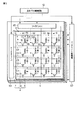
図1は、発明に先立って検討した表示装置の構成を示す断面図である。
図1に示す表示装置100は、保護カバー2、タッチパネル3、ディスプレイ部4、及びバックライト5を備えている。なお、ディスプレイ部4は、例えば、液晶表示パネルである。ディスプレイ部4はOLED(有機発光ダイオード)を用いた薄型ディスプレイとして形成されても良い。OLEDのような自発光ディスプレイの場合、バックライト5は、不要である。
[First Embodiment]
FIG. 1 is a cross-sectional view showing the configuration of a display device studied prior to the invention.
A
タッチパネル3は、タッチ信号用電極3aとタッチパネル電極基板3bを備えている。タッチ信号用電極3aは、タッチ用接続部品11aを介してタッチ信号制御回路11に電気的に接続する。タッチパネル3は、指などの誘電体の接近(接触)位置を電極3aの容量変化によって検知する。タッチパネル3は、ITO(Indium Tin Oxide)や銀ナノワイヤなどの素材を使用した透明電極で、例えば、縦横からなる多数のモザイク状電極パターンとしてガラス、プラスチックなどの基板上に配置される。
The
ディスプレイ部4は、一対の基板であるアレイ基板7および対向基板8間に液晶層LQを挟持した構造である。更に、アレイ基板7および対向基板8の液晶層と反対側にはそれぞれ偏光板PL1、PL2が設けられている。IPS液晶では、アレイ基板7に設けられた画素電極PE(図示せず)およびコモン電極CE(図示せず)から液晶層LQに印加される液晶駆動電圧により液晶層LQの透過率が制御される。画素電極PEおよびコモン電極CEは、表示用電極12aを介して表示パネル制御回路12に接続する。
The
保護カバー2は、タッチパネル3、及びディスプレイ部4を外部からの衝撃に対して保護する。保護カバー2は、ガラスであるが、アクリルやポリカーボネートやPETなど透明な誘電体として形成されても良い。
The
図1に示す表示装置は、外付け方式であるため、専用のタッチパネル部3、及びタッチ用接続部品11aが必要となっていた。
Since the display device shown in FIG. 1 is an external system, a dedicated
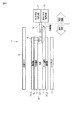
次に、タッチパネル3及びディスプレイ部4の回路構成と動作原理について説明する。
Next, circuit configurations and operation principles of the
図2は、タッチパネル3の構成を示す模式図である。
FIG. 2 is a schematic diagram illustrating the configuration of the
タッチパネル3は、左右方向に延線する複数の透明な行電極(1行、2行、・・・)と、上下方向に延線する複数の透明な列電極(A列、B列、・・・)とが格子状に設けられている。なお、行電極と列電極は、透明絶縁膜を介し異なる層に配置されている。例えば、行電極はタッチパネル電極基板3bに設けられ、列電極はタッチ信号用電極3aとして構成することができる。
The
図2には、指がタッチパネル3の第2行の行電極と、第A列の列電極の交点近傍に接触した状態を示している。このときは、誘電体である指の存在によって第2行の行電極と第A列の列電極との相互容量が変化する。従って、行電極と列電極との相互容量を測定することで、指の存在位置を検知することができる。
FIG. 2 shows a state where the finger is in contact with the vicinity of the intersection of the row electrode of the second row of the
なお、誘電体である指の存在によって第2行の行電極の自己容量、あるいは第A列の列電極の自己容量が変化する。ここで、自己容量とは、行電極又は列電極の各々と、周囲の導電体との間に存在する容量を指す。従って、指の接触による行電極あるいは列電極との自己容量の変化を測定することで、指の存在位置を検知することもできる。 Note that the self-capacitance of the row electrode of the second row or the self-capacitance of the column electrode of the A-th column changes due to the presence of the dielectric finger. Here, the self-capacitance refers to a capacitance existing between each row electrode or column electrode and a surrounding conductor. Therefore, the position of the finger can also be detected by measuring the change in self-capacitance with the row electrode or the column electrode due to the finger contact.
検知動作は、例えば、次のように実行される。 The detection operation is executed as follows, for example.
タッチ信号制御回路11は、1行目の行電極に信号を供給して列電極(A列、B列、・・・)のそれぞれの電極の信号を読み取る。読み取った信号には、行電極と列電極の相互容量に関する情報が含まれている。次に、2行目の行電極に信号を供給して列電極(A列、B列、・・・)のそれぞれの電極の信号を読み取る。この動作を行電極を順次切り替えて実行することで、指の存在位置(行電極位置及び列電極位置)を検知することができる。なお、この動作は、タッチ信号制御回路11が交流波形信号(例えば、矩形波信号)を出力し、その交流波形信号に同期して供給する行電極を切り替え、列電極(A列、B列、・・・)のそれぞれの電極の信号を読み取ることで実現することができる。
The touch
図3は、表示装置1の表示に関わる回路構成を概略的に示す図である。なお、以下の説明ではIPS液晶について説明するが、後述するように本願はIPS液晶に限定されず、他の横電界方式の液晶表示装置、縦電界方式の液晶表示装置、有機EL表示装置などにも広く適用することができる。 FIG. 3 is a diagram schematically showing a circuit configuration relating to display of the display device 1. In the following description, the IPS liquid crystal will be described. However, as will be described later, the present application is not limited to the IPS liquid crystal. Can also be widely applied.
表示装置1は、ディスプレイ部4、ディスプレイ部4を照明するバックライト5、及び表示パネル制御回路12を備える。ディスプレイ部4は、上述のように一対の基板であるアレイ基板7および対向基板8間に液晶層LQを挟持した構造である。表示パネル制御回路12は、液晶層LQに印加される液晶駆動電圧を制御してディスプレイ部4の透過率を制御する。
The display device 1 includes a
アレイ基板7では、複数の画素電極PEがアレイガラス基板GL上において略マトリクス状に配置される。また、複数のゲート線Y(Y1〜Ym)が複数の画素電極PEの行に沿って配置され、複数のソース線X(X1〜Xn)が複数の画素電極PEの列に沿って配置される。また、アレイ基板7には、コモン電極CEが画素電極PEと別のレイヤーに設けられている。
In the
これらゲート線Yおよびソース線Xの交差位置近傍には、複数の画素スイッチング素子Wが配置される。各画素スイッチング素子Wは例えばゲートがゲート線Yに接続され、ソース−ドレインパスがソース線Xおよび画素電極PE間に接続される薄膜トランジスタからなり、対応ゲート線Yを介して駆動されたときに対応ソース線Xおよび対応画素電極PE間で導通する。 A plurality of pixel switching elements W are arranged in the vicinity of the intersection position of the gate line Y and the source line X. Each pixel switching element W is formed of a thin film transistor in which a gate is connected to the gate line Y and a source-drain path is connected between the source line X and the pixel electrode PE, and corresponds to when driven through the corresponding gate line Y. Conduction is established between the source line X and the corresponding pixel electrode PE.
各画素電極PEおよびコモン電極CEのそれぞれは、配向膜で覆われ、画素電極PEおよびコモン電極CEからの電界に対応した液晶分子配列に制御される液晶層LQの一部である画素領域と共に液晶画素PXを構成する。 Each of the pixel electrodes PE and the common electrode CE is covered with an alignment film, and liquid crystal together with a pixel region that is a part of the liquid crystal layer LQ that is controlled to a liquid crystal molecular arrangement corresponding to the electric field from the pixel electrode PE and the common electrode CE. A pixel PX is configured.
複数の液晶画素PXは各々画素電極PEおよびコモン電極CE間に液晶容量CLCを有する。複数の補助容量線C1〜Cmは各々対応行の液晶画素PXの画素電極PEに容量結合した補助容量Csを構成する。補助容量Csは画素スイッチング素子Wの寄生容量に対して十分大きな容量値を有する。 Each of the plurality of liquid crystal pixels PX has a liquid crystal capacitor CLC between the pixel electrode PE and the common electrode CE. Each of the plurality of auxiliary capacitance lines C1 to Cm constitutes an auxiliary capacitance Cs that is capacitively coupled to the pixel electrode PE of the liquid crystal pixel PX in the corresponding row. The auxiliary capacitor Cs has a sufficiently large capacitance value with respect to the parasitic capacitance of the pixel switching element W.
表示パネル制御回路12は、ゲートドライバYD、ソースドライバXDの動作を制御する。
ゲートドライバYDは、複数のスイッチング素子Wを行単位に導通させるように複数のゲート線Y1〜Ymを順次駆動する。ソースドライバXDは、各行のスイッチング素子Wが対応ゲート線Yの駆動によって導通する期間において画素電圧Vsを複数のソース線X1〜Xnにそれぞれ出力する。バックライト駆動部LDは、バックライト5の点消灯動作を制御する。
The display
The gate driver YD sequentially drives the plurality of gate lines Y1 to Ym so that the plurality of switching elements W are conducted in units of rows. The source driver XD outputs the pixel voltage Vs to the plurality of source lines X1 to Xn in a period in which the switching elements W in each row are turned on by driving the corresponding gate line Y. The backlight drive unit LD controls the turning on / off operation of the
対向基板8には、カラーフィルタ、ブラックマトリクスがそれぞれの画素に対応して配設されている。カラーフィルタは、サブ画素に対応して、それぞれR(赤)、G(緑)、B(青)の光を透過させる着色層である。ブラックマトリクスは、各色のカラーフィルタの境界部に設けられる不透明の物質であって、表示装置1が黒色を表示する際の光漏れ、隣接する着色層間での光の混色を防止する。
On the
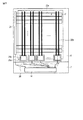
図4は、第1の実施の形態に係る表示装置1の基本の構成を示す図である。
図4に示す表示装置1では、タッチ信号用電極3aが対向基板8と偏光板PL1との間に設けられ、タッチパネル電極基板3bは設けられていない。後述するが、タッチパネル電極基板3bの機能は、ディスプレイ部4の、例えば、アレイ基板7側に組み込まれている。そして、タッチ信号用電極3aは、容量結合15によってアレイ基板7側の電極に接続される。即ち、タッチ信号はアレイ基板7を介して外部に設けられるタッチ信号制御回路11と送受信される。アレイ基板7側で外部回路(タッチ信号制御回路11、表示パネル制御回路12)との信号授受を一括して行うことができるため、タッチ用信号線と表示用信号線とをアレイ基板側において共用することが可能となる。
FIG. 4 is a diagram illustrating a basic configuration of the display device 1 according to the first embodiment.
In the display device 1 shown in FIG. 4, the touch signal electrode 3a is provided between the
このように第1の実施の形態によれば、タッチパネル電極基板3bを設けず、タッチ信号の授受を、対向基板8側のタッチ信号用電極3aとアレイ基板7側の電極との間の容量結合を介して行い、外部回路との接続を、表示用の接続部品を経由して行うことができるため、薄型化と低コスト化を可能とすることができる。
As described above, according to the first embodiment, the touch panel electrode substrate 3b is not provided, and the touch signal is exchanged by capacitive coupling between the touch signal electrode 3a on the
続いて、第1の実施の形態の表示装置1におけるタッチ機能を実現する構成について説明する。なお、以下の記載では、参照符号は適宜変更して使用するため、上記記載とはことなる場合のあることに留意されたい。 Next, a configuration for realizing the touch function in the display device 1 according to the first embodiment will be described. In the following description, it should be noted that the reference numerals may be changed as appropriate and may be different from the above description.
[横電界方式の液晶を用いた構成]
図5は、第1の実施の形態の表示装置のIPS液晶を用いた際の構成を示す平面図である。
[Configuration using horizontal electric field type liquid crystal]
FIG. 5 is a plan view showing a configuration when the IPS liquid crystal of the display device according to the first embodiment is used.
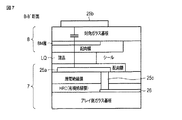
アレイ基板7には、タッチ行電極20a、タッチ信号ドライバ21、共用電極14、アレイ側容量電極25a、及び接続線26が設けられている。対向基板8には、タッチ列電極20b、及び対向側容量電極25bが備えられている。
The
タッチ行電極20aは、図2に示す行電極(1行、2行、・・・)に相当する。タッチ信号ドライバ21は、タッチ行電極20aに交流波形信号(例えば、矩形波信号)を出力する。タッチ列電極20bには、タッチ行電極20aとの間の相互容量と、タッチ列電極20bの自己容量とに応じた信号(タッチ信号)が生起される。対向側容量電極25bは、アレイ側容量電極25aと容量結合されている。生起した信号は、アレイ側容量電極25aを介して共用電極14に送られる。共用電極14と、タッチ信号ドライバ21及びアレイ側容量電極25aとの間は、接続線26によって電気的に接続されている。
The
図6は、図5のA−A’に沿う断面図である。液晶層LQは、アレイ基板7と対向基板8とに挟持されている。
FIG. 6 is a cross-sectional view taken along A-A ′ in FIG. 5. The liquid crystal layer LQ is sandwiched between the
アレイ基板7は、アレイガラス基板上に有機絶縁膜(HRC)を介してコモン電極CEを配している。コモン電極CEはSiN膜等の層間絶縁膜で覆われ、層間絶縁膜上に画素電極PEが配されている。そして、アレイ基板7の液晶層LQと接する側の面には、配向膜が設けられている。対向基板8は、対向ガラス基板上にブラックマトリクス(BM)層とカラーフィルタ(CF)層とを備え、更に液晶層LQと接する側の面に配向膜を設けている。
The
そして、タッチ行電極20aは、アレイ基板7のコモン電極CEと共用され、タッチ列電極20bは、対向基板8の対向ガラス基板の液晶層LQと反対側の面に設けられている。
The
図7は、図5のB−B’に沿う断面図である。アレイ基板7及び対向基板8の構成については既に説明しているため、重複した説明は省略する。
FIG. 7 is a cross-sectional view taken along B-B ′ in FIG. 5. Since the configurations of the
アレイ側容量電極25aは、透明電極とすることで、SiN膜等の層間絶縁膜上に画素電極PE等を形成する透明電極と同一工程で形成することができる。また、接続線26は、アレイガラス基板上に設けられている。そして、アレイ側容量電極25aと接続線26とは透明のコンタクト電極25cによって電気的に接続することでアレイ側容量電極25aを形成する透明電極と同一工程で形成することができる。対向側容量電極25bは、透明電極とすることで、タッチ列電極20bと同一工程で形成することができる。
The array-
図5〜図7に示すように、タッチ行電極20aをアレイ基板7のコモン電極CEと共用することによってタッチパネル電極基板3bが不要となるため、表示装置1の厚みを低減することが可能となる。また、対向基板側に設けられる容量電極25bとアレイ基板側の額縁に設けられる容量電極25aとを容量結合させることにより、タッチ信号をアレイ基板上の電極に取り出すことができる。さらに表示動作とタッチ動作とをタイムシェアリングすることによって、表示用電極信号との共用を図ることが可能となり部品削減などのコスト削減を図ることができる。
As shown in FIGS. 5 to 7, since the
なお、図6ではタッチ列電極20bは、対向基板8の対向ガラス基板の液晶層LQと反対側の面に設けられているが、さらに偏光板PL1の液晶層LQと反対側の面に設けても良い。また、対向基板8の対向ガラス基板の液晶層LQ側の面に設けても良い。但し、表示動作への影響を考慮した場合は、対向ガラス基板の液晶層LQと反対側の面に設けることが望ましい。
In FIG. 6, the
[縦電界方式の液晶を用いた構成−その1]
図8は、第1の実施の形態の表示装置の縦電界方式の液晶を用いた際の構成を示す平面図である。縦電界方式の液晶を使用する表示装置では、コモン電極CEが対向基板8側に設けられている。このため、タッチ行電極20aも対向基板8側に設けられる。
[Configuration using vertical electric field type liquid crystal-1]
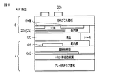
FIG. 8 is a plan view showing a configuration when the vertical electric field type liquid crystal of the display device of the first embodiment is used. In a display device using a vertical electric field type liquid crystal, the common electrode CE is provided on the
アレイ基板7には、タッチ信号ドライバ21、共用電極14、アレイ側容量電極25a、接続線26、及びアレイ側接続パッド31が設けられている。対向基板8には、タッチ行電極20a、タッチ列電極20b、及び対向側容量電極25bが備えられている。
The
タッチ行電極20aが対向基板8に設けられているため、アレイ基板7側の電極とタッチ行電極20aとを電気的に接続させるためのアレイ側接続パッド31が新たに設けられている。タッチ行電極20aとアレイ側接続パッド31以外の構成要素の配置については上述と同様であるため、その説明は省略する。
Since the
図9は、図8のA−A’に沿う断面図である。液晶層LQは、アレイ基板7と対向基板8とに挟持されている。
FIG. 9 is a cross-sectional view taken along A-A ′ of FIG. 8. The liquid crystal layer LQ is sandwiched between the
アレイ基板7は、アレイガラス基板上に有機絶縁膜(HRC)を介して補助容量電極CsEを配している。補助容量電極CsEはSiN等の層間絶縁膜で覆われ、層間絶縁膜上に画素電極PEが配されている。そして、アレイ基板7の液晶層LQと接する側の面には、配向膜が設けられている。対向基板8は、対向ガラス基板上にブラックマトリクス(BM)層とカラーフィルタ(CF)層とを備え、更に液晶層LQと接する側の面にコモン電極CEを設けている。そして、ブラックマトリクス(BM)層、カラーフィルタ(CF)、及びタッチ行電極20aを覆うように配向膜を設けている。
The
そして、タッチ行電極20aは、対向基板8のコモン電極CEと共用され、タッチ列電極20bは、対向基板8の対向ガラス基板の液晶層LQと反対側の面に設けられている。
The
図10は、図8のB−B’に沿う断面図である。図10は、図7に示す断面図と同じ構成であるため、重複した説明は省略する。 FIG. 10 is a sectional view taken along B-B ′ of FIG. 8. 10 has the same configuration as the cross-sectional view shown in FIG.
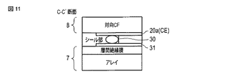
図11は、図8のC−C’に沿う断面図である。タッチ信号ドライバ21の出力端子にはアレイ側接続パッド31が設けられる。対向基板8側に設けられたタッチ行電極20a(コモン電極CE)は、例えば、アレイ側接続パッド31と導電性微粒子であるAuめっきパール材30等を介して電気的に接続されている。これにより、タッチ信号ドライバ21は、タッチ行電極20aに交流波形信号を供給することができる。
FIG. 11 is a cross-sectional view taken along C-C ′ in FIG. 8. An array
[縦電界方式の液晶を用いた構成−その2]
図12は、第1の実施の形態の表示装置の縦電界方式の液晶を用いた際の構成を示す平面図である。縦電界方式の液晶を使用する表示装置では、コモン電極CEが対向基板8側に設けられている。このため、タッチ行電極20aも対向基板8側に設けられる。
[Configuration using vertical electric field type liquid crystal-2]
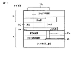
FIG. 12 is a plan view showing a configuration when the vertical electric field type liquid crystal of the display device of the first embodiment is used. In a display device using a vertical electric field type liquid crystal, the common electrode CE is provided on the
アレイ基板7には、共用電極14、アレイ側容量電極25a、接続線26、及びアレイ側接続パッド31が設けられている。対向基板8には、タッチ行電極20a、タッチ列電極20b、対向側容量電極25b、及び配線27が備えられている。
The
配線27が対向基板8に設けられているため、アレイ基板7側の電極と配線27とを電気的に接続させるためのアレイ側接続パッド31が新たに設けられている。アレイ基板7には、タッチ信号ドライバ21は設けられていない。タッチ行電極20a、アレイ側接続パッド31、配線27以外の構成要素の平面配置については上述と同様であるため、その説明は省略する。
Since the
図13は、図12のA−A’に沿う断面図である。液晶層LQは、アレイ基板7と対向基板8とに挟持されている。
FIG. 13 is a cross-sectional view taken along A-A ′ of FIG. 12. The liquid crystal layer LQ is sandwiched between the
アレイ基板7は、アレイガラス基板上に有機絶縁膜(HRC)を介して補助容量電極CsEを配している。補助容量電極CsEはSiN等の層間絶縁膜で覆われ、層間絶縁膜上に画素電極PEが配されている。そして、アレイ基板7の液晶層LQと接する側の面には、配向膜が設けられている。対向基板8は、対向ガラス基板上にブラックマトリクス(BM)層とカラーフィルタ(CF)層とを備えている。タッチ行電極20aとブラックマトリクス層とは平面図で同じ位置に設けられている。そして、ブラックマトリクス(BM)層、カラーフィルタ(CF)、及びタッチ行電極20aを覆うように配向膜を設けている。なお、タッチ行電極20aはブラックマトリクス層と共用するように構成しても良い。
The
そして、タッチ列電極20bは、対向基板8の対向ガラス基板の液晶層LQと反対側の面に設けられている。
The
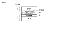
図14は、図12のB−B’に沿う断面図である。図14は、図7に示す断面図と同じ構成であるため、重複した説明は省略する。 FIG. 14 is a cross-sectional view taken along B-B ′ in FIG. 12. FIG. 14 has the same configuration as the cross-sectional view shown in FIG.
図15は、図12のC−C’に沿う断面図である。アレイ基板7には外部のコントロール回路に接続するアレイ側接続パッド31が設けられる。対向基板8側に設けられた配線27は、アレイ側接続パッド31と導電性微粒子であるAuめっきパール材30等を介して電気的に接続されている。そして、配線27とタッチ行電極20aとが接続されている。
FIG. 15 is a cross-sectional view taken along C-C ′ in FIG. 12. The
図12〜図15に示す縦電界方式の液晶を用いた構成(その2)では、タッチ信号ドライバ21を内蔵せずに外部から直接信号を供給している。従って、図8〜図11に示す縦電界方式の液晶を用いた構成(その1)と比較すると、ドライバ回路とアレイ側接続パッドを同一個所にまとめて配置する必要がないため、額縁幅を縮小することが可能となる。
In the configuration (No. 2) using the vertical electric field type liquid crystal shown in FIGS. 12 to 15, the signal is directly supplied from the outside without including the
また、構成(その2)では、タッチ行電極20aは透明電極ではなく、不透明なメタル電極で構成し、コモン電極CEとは別に、BM兼用、もしくはBMからはみ出さないように形成する。タッチ行電極20aに従来の透明電極を用いた場合は、額縁引き回し部の配線抵抗が高くなるが、メタル電極は透明電極に比較して抵抗が低いため、額縁部の引き回し配線を細かいコンパクトなパターンで形成することが可能となる。
In the configuration (No. 2), the
図12〜図15に示すように、タッチ行電極20aを不透明なメタル電極で構成し、コモン電極CEとは別に、BM兼用、もしくはBMからはみ出さないように形成することによってタッチパネル電極基板3bが不要となるため、表示装置1の厚みを低減することが可能となる。また、対向基板側に設けられる電極とアレイ基板側の額縁に設けられる電極とを容量結合させることにより、タッチ信号をアレイ基板上の電極に取り出すことができる。また、額縁部の引き回し配線を細かいコンパクトなパターンで形成して額縁幅を縮小することが可能となる。さらに表示動作とタッチ動作とをタイムシェアリングすることによって、表示用電極信号とタッチ信号との共用を図ることが可能となり部品削減などのコスト削減を図ることができる。
As shown in FIGS. 12 to 15, the
なお、図13ではタッチ列電極20bは、対向基板8の対向ガラス基板の液晶層LQと反対側の面に設けられているが、さらに偏光板PL1の液晶層LQと反対側の面に設けても良い。また、対向基板8の対向ガラス基板の液晶層LQ側の面に設けても良い。但し、表示動作への影響を考慮した場合は、対向ガラス基板の液晶層LQと反対側の面に設けることが望ましい。
In FIG. 13, the
[有機発光ダイオード(OLED)を用いた構成]
図16は、第1の実施の形態の表示装置のOLEDを用いた際の構成を示す平面図である。OLEDを使用する表示装置では、液晶で使用されるコモン電極CEは存在しない。
[Configuration using organic light emitting diode (OLED)]
FIG. 16 is a plan view showing a configuration when the OLED of the display device according to the first embodiment is used. In a display device using OLED, there is no common electrode CE used for liquid crystal.
アレイ基板7には、共用電極14、アレイ側容量電極25a、接続線26、配線27、及びアレイ側接続パッド31が設けられている。対向基板8には、タッチ行電極20a、タッチ列電極20b、対向側容量電極25bが備えられている。
The
配線27が対向基板8に設けられているため、アレイ基板7側の電極と配線27とを電気的に接続させるためのアレイ側接続パッド31が新たに設けられている。アレイ基板7には、タッチ信号ドライバ21は設けられていない。タッチ行電極20a、アレイ側接続パッド31、配線27以外の構成要素の平面配置については上述と同様であるため、その説明は省略する。
Since the
図17は、図16のA−A’に沿う断面図である。アレイ基板7と対向基板8とは充填剤層を挟持している。
FIG. 17 is a cross-sectional view taken along A-A ′ of FIG. 16. The
アレイ基板7は、アレイガラス基板上にOLEDとOLED駆動回路35を配したバリア層を設けている。OLEDは、OLED陰極とOLED陽極との間に発光層を挟持して構成されている。
The
対向基板8は、対向ガラス基板上にブラックマトリクス(BM)層とカラーフィルタ(CF)層とを備えている。そして、タッチ行電極20aとブラックマトリクス層とは平面図で同じ位置に設けられている。なお、タッチ行電極20aはブラックマトリクス層と共用するように構成しても良い。
The
そして、タッチ列電極20bは、対向基板8の対向ガラス基板の充填剤層と反対側の面に設けられている。
The
図18は、図16のB−B’に沿う断面図である。 18 is a cross-sectional view taken along B-B ′ of FIG.
アレイ側容量電極25aは、透明電極であり、バリア層上に設けられている。また、接続線26は、アレイガラス基板上に設けられている。そして、アレイ側容量電極25aと接続線26とは透明のコンタクト電極25cによって電気的に接続されている。対向側容量電極25bは、透明電極であり、タッチ列電極20bと同層に形成されている。
The array-
なお、図18ではバリア層を貫通するコンタクト電極25cを設けているが、バリア層に貫通孔を設ける際には湿式の工程を用いるため、必ずしもOLEDに適した製造方法であるとは言えない。従って、バリエーションの構成として、アレイ側容量電極25aをバリア層の外部まで引き伸ばし、外部で接続線26と電気的に接続しても良い。
In FIG. 18, the
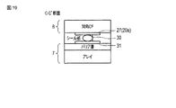
図19は、図16のC−C’に沿う断面図である。 FIG. 19 is a cross-sectional view taken along C-C ′ in FIG. 16.
アレイ基板7には外部のコントロール回路に接続するアレイ側接続パッド31が設けられる。対向基板8側に設けられた配線27は、アレイ側接続パッド31と導電性微粒子であるAuめっきパール材30等を介して電気的に接続されている。そして、配線27とタッチ行電極20aとが電気的に接続されている。
The
図16〜図19に示すOLEDを用いた構成では、タッチ行電極20aは透明電極ではなく、不透明なメタル電極で構成し、BM兼用、もしくはBMからはみ出さないように形成する。タッチ行電極20aに従来の透明電極を用いた場合は、額縁引き回し部の配線抵抗が高くなるとの問題があったが、メタル電極は透明電極に比較して抵抗が低いため、額縁部の引き回し配線を細かいコンパクトなパターンで形成することが可能となる。
In the configuration using the OLED shown in FIGS. 16 to 19, the
図16〜図19に示すように、タッチ行電極20aを不透明なメタル電極で構成し、BM兼用、もしくはBMからはみ出さないように形成することによってタッチパネル電極基板3bが不要となるため、表示装置1の厚みを低減することが可能となる。また、対向基板側に設けられる電極とアレイ基板側の額縁に設けられる電極とを容量結合させることにより、タッチ信号をアレイ基板上の電極に取り出すことができる。また、額縁部の引き回し配線を細かいコンパクトなパターンで形成して額縁幅を縮小することが可能となる。さらに表示動作とタッチ動作とをタイムシェアリングすることによって、表示用電極信号の共用を図ることが可能となり部品削減などのコスト削減を図ることができる。
As shown in FIGS. 16 to 19, the
[第2の実施の形態]
図20は、第2の実施の形態に係る表示装置1の基本の構成を示す図である。第1の実施の形態と同一の部位には同一の符号を付してその詳細の説明は省略する。
[Second Embodiment]
FIG. 20 is a diagram illustrating a basic configuration of the display device 1 according to the second embodiment. The same parts as those in the first embodiment are denoted by the same reference numerals, and detailed description thereof is omitted.
第2の実施の形態では、アレイ基板上に増幅回路(AMP)40を設け、増幅した信号に変換するように構成する。これによって外部の回路構成が簡略化され、タッチ性能の向上と外部回路の低コスト化を図ることができる。 In the second embodiment, an amplifier circuit (AMP) 40 is provided on the array substrate so as to convert it into an amplified signal. As a result, the external circuit configuration is simplified, and the touch performance can be improved and the cost of the external circuit can be reduced.
[第3の実施の形態]
図21は、第3の実施の形態に係る表示装置1の基本の構成を示す図である。第1の実施の形態と同一の部位には同一の符号を付してその詳細の説明は省略する。
[Third embodiment]
FIG. 21 is a diagram illustrating a basic configuration of the display device 1 according to the third embodiment. The same parts as those in the first embodiment are denoted by the same reference numerals, and detailed description thereof is omitted.
第3の実施の形態では、アレイ基板上に増幅変換回路(AMP+ADC)41を設け、信号を増幅してデジタル信号に変換して(A/D変換して)出力するように構成する。これによって外部の回路構成が簡略化され、タッチ性能の向上とタッチ信号制御回路11の更なる簡略化を図ることができる。
In the third embodiment, an amplification conversion circuit (AMP + ADC) 41 is provided on the array substrate, and a signal is amplified and converted into a digital signal (A / D conversion) for output. Thereby, the external circuit configuration is simplified, and the touch performance can be improved and the touch
上述のいくつかの実施形態は、例として提示したものであり、発明の範囲を限定することは意図していない。これら新規な実施形態は、その他の様々な形態で実施されることが可能であり、発明の要旨を逸脱しない範囲で、種々の省略、置き換え、変更を行うことができる。これら実施形態やその変形は、発明の範囲や要旨に含まれるとともに、特許請求の範囲に記載された発明とその均等の範囲に含まれる。 The several embodiments described above have been presented by way of example and are not intended to limit the scope of the invention. These novel embodiments can be implemented in various other forms, and various omissions, replacements, and changes can be made without departing from the scope of the invention. These embodiments and modifications thereof are included in the scope and gist of the invention, and are included in the invention described in the claims and the equivalents thereof.
例えば、上述の実施の形態では、タッチ行電極20aを補助容量電極CsE、コモン電極CE、BM25などと共用したが、タッチ行電極20aをゲート線Y、ソース線Xと共有するように構成しても良い。
For example, in the above-described embodiment, the
また、タッチ行電極20aに交流波形信号を入力し、タッチ列電極20bからタッチ信号を読み取ったが、逆にタッチ列電極20bに交流波形信号を入力し、タッチ行電極20aからタッチ信号を読み取っても良い。
Further, an AC waveform signal is input to the
さらに、自己容量方式を採用してタッチ列電極20bの一部に交流波形信号を入力し、残りのタッチ列電極20bから信号を読み取ってタッチ位置を検知するように構成しても良い。
Further, a self-capacitance method may be adopted so that an AC waveform signal is input to a part of the
また、対向基板8は偏光板を含んで構成し、タッチ列電極20bを偏光板の上面に設けても良い。
Further, the
また、アレイ基板7上にある駆動素子は低温ポリシリコンTFTで構成することができる。これによって、額縁を広く使用することができ、開口を大きくすることができる。
The driving element on the
また、アレイ基板7上にある駆動素子は酸化物TFTで構成することができる。これによって、コストを更に低減することができる。
The driving element on the
また、アレイ基板7上にある駆動素子は有機薄膜TFTで構成することができる。これによって、柔軟なディスプレイ部を形成することができる。
Further, the driving element on the
LQ…液晶層、PE…画素電極、CE…コモン電極、GL…アレイガラス基板、Y…ゲート線、X…ソース線、C1〜Cm…補助容量線、CsE…補助容量電極、PL1、PL2…偏光板、1…表示装置、3…タッチパネル、3a…タッチ信号用電極、3b…タッチパネル電極基板、4…ディスプレイ部、5…バックライト、7…アレイ基板、8…対向基板、11a…タッチ用接続部品、11…タッチ信号制御回路、12a…表示用電極、12…表示パネル制御回路、14…共用電極、20a…タッチ行電極、20b…タッチ列電極、21…タッチ信号ドライバ、25a…アレイ側容量電極、25b…対向側容量電極、25c…コンタクト電極、26…接続線、27…配線、30…パール材、31…アレイ側接続パッド、35…OLED駆動回路、40…増幅回路、41…増幅変換回路。
LQ ... liquid crystal layer, PE ... pixel electrode, CE ... common electrode, GL ... array glass substrate, Y ... gate line, X ... source line, C1-Cm ... auxiliary capacitance line, CsE ... auxiliary capacitance electrode, PL1, PL2 ... polarized light Plate: 1
Claims (9)
前記アレイ基板と対向しブラックマトリクスを有する対向基板と、
第1方向に延線する複数の透明な第1電極群と、
前記第1方向と交差する第2方向に延線する複数の透明な第2電極群と、
前記第1電極群に駆動信号を供給する駆動回路と、
前記第2電極群から前記駆動信号に対応するタッチ検知信号を取得する検知回路と、を有し、
前記第2電極群は前記対向基板の一層に形成され、
前記第1電極群は前記アレイ基板または対向基板の一層に形成され、
前記タッチ検知信号は、前記対向基板側からアレイ基板側に容量結合によって伝達されるようになされる、表示装置。 An array substrate having a plurality of pixel electrodes or light emitting elements arranged in a matrix;
A counter substrate facing the array substrate and having a black matrix;
A plurality of transparent first electrode groups extending in a first direction;
A plurality of transparent second electrode groups extending in a second direction intersecting the first direction;
A drive circuit for supplying a drive signal to the first electrode group;
A detection circuit that acquires a touch detection signal corresponding to the drive signal from the second electrode group,
The second electrode group is formed on one layer of the counter substrate,
The first electrode group is formed on one layer of the array substrate or the counter substrate,
The display device, wherein the touch detection signal is transmitted from the counter substrate side to the array substrate side by capacitive coupling.
前記第1の電極群は、前記アレイ基板のコモン電極と共用され、
前記第2の電極群は、前記対向基板の絶縁基板の背面側に形成される、
請求項1に記載の表示装置。 The display device sandwiches a horizontal electric field type liquid crystal layer between the array substrate and a counter substrate,
The first electrode group is shared with the common electrode of the array substrate,
The second electrode group is formed on the back side of the insulating substrate of the counter substrate.
The display device according to claim 1.
前記第1の電極群は、前記対向基板のコモン電極と共用され、
前記第2の電極群は、前記対向基板の絶縁基板の背面側に形成される、
請求項1に記載の表示装置。 The display device sandwiches a vertical electric field type liquid crystal layer between the array substrate and a counter substrate,
The first electrode group is shared with the common electrode of the counter substrate,
The second electrode group is formed on the back side of the insulating substrate of the counter substrate.
The display device according to claim 1.
前記駆動回路と前記第1の電極群とが導電性微粒子を介して電気的に接続される、
請求項3に記載の表示装置。 The drive circuit is provided on the frame of the array substrate,
The drive circuit and the first electrode group are electrically connected via conductive fine particles,
The display device according to claim 3.
前記第1の電極群は、前記対向基板の前記ブラックマトリクスと共用され、あるいは平面図において前記対向基板の前記ブラックマトリクスの領域内にコモン電極と共用されて形成され、
前記第2の電極群は、前記対向基板の絶縁基板の背面側に形成される、
請求項1に記載の表示装置。 The display device sandwiches a vertical electric field type liquid crystal layer between the array substrate and a counter substrate,
The first electrode group is shared with the black matrix of the counter substrate, or is shared with a common electrode in a region of the black matrix of the counter substrate in a plan view,
The second electrode group is formed on the back side of the insulating substrate of the counter substrate.
The display device according to claim 1.
前記第1の電極群は、前記対向基板の前記ブラックマトリクスと共用され、あるいは平面図において前記対向基板の前記ブラックマトリクスの領域内に形成され、
前記第2の電極群は、前記対向基板の絶縁基板の背面側に形成される、
請求項1に記載の表示装置。 The display device sandwiches a filler between the array substrate including a light emitting element and a counter substrate,
The first electrode group is shared with the black matrix of the counter substrate, or formed in a region of the black matrix of the counter substrate in a plan view,
The second electrode group is formed on the back side of the insulating substrate of the counter substrate.
The display device according to claim 1.
前記信号端子と前記第1の電極群とが導電性微粒子を介して電気的に接続される、
請求項5又は6に記載の表示装置。 The frame of the array substrate is provided with a signal terminal from the drive circuit outside the array substrate,
The signal terminal and the first electrode group are electrically connected via conductive fine particles,
The display device according to claim 5 or 6.
増幅されたタッチ検知信号をデジタル化して、前記アレイ基板の外部の前記検知回路に出力するデジタル変換回路を更に有する、請求項1乃至7のうちのいずれか1項に記載の表示装置。 An analog amplification circuit that amplifies a touch detection signal transmitted to the array substrate side by the capacitive coupling;
The display device according to claim 1, further comprising a digital conversion circuit that digitizes the amplified touch detection signal and outputs the digitized touch detection signal to the detection circuit outside the array substrate.
Priority Applications (1)
| Application Number | Priority Date | Filing Date | Title |
|---|---|---|---|
| JP2013143799A JP6306295B2 (en) | 2013-07-09 | 2013-07-09 | Display device |
Applications Claiming Priority (1)
| Application Number | Priority Date | Filing Date | Title |
|---|---|---|---|
| JP2013143799A JP6306295B2 (en) | 2013-07-09 | 2013-07-09 | Display device |
Related Child Applications (1)
| Application Number | Title | Priority Date | Filing Date |
|---|---|---|---|
| JP2018039957A Division JP6564896B2 (en) | 2018-03-06 | 2018-03-06 | Display device |
Publications (3)
| Publication Number | Publication Date |
|---|---|
| JP2015018331A true JP2015018331A (en) | 2015-01-29 |
| JP2015018331A5 JP2015018331A5 (en) | 2016-08-25 |
| JP6306295B2 JP6306295B2 (en) | 2018-04-04 |
Family
ID=52439282
Family Applications (1)
| Application Number | Title | Priority Date | Filing Date |
|---|---|---|---|
| JP2013143799A Active JP6306295B2 (en) | 2013-07-09 | 2013-07-09 | Display device |
Country Status (1)
| Country | Link |
|---|---|
| JP (1) | JP6306295B2 (en) |
Cited By (4)
| Publication number | Priority date | Publication date | Assignee | Title |
|---|---|---|---|---|
| US10379681B2 (en) | 2016-07-20 | 2019-08-13 | Japan Display Inc. | Touch sensor having waveguides and display device including the touch sensor |
| US10564462B2 (en) | 2016-07-19 | 2020-02-18 | Japan Display Inc. | Touch sensor and display device |
| US10872934B2 (en) | 2016-07-01 | 2020-12-22 | Japan Display Inc. | Display device and manufacturing method thereof |
| WO2021024677A1 (en) * | 2019-08-02 | 2021-02-11 | 株式会社ジャパンディスプレイ | Display system and display device |
Citations (8)
| Publication number | Priority date | Publication date | Assignee | Title |
|---|---|---|---|---|
| JP2009244958A (en) * | 2008-03-28 | 2009-10-22 | Sony Corp | Display device with touch sensor |
| JP2010277443A (en) * | 2009-05-29 | 2010-12-09 | Sony Corp | Touch sensor, display device, and electronic equipment |
| JP2011070092A (en) * | 2009-09-28 | 2011-04-07 | Sharp Corp | Liquid crystal display device |
| JP2011138316A (en) * | 2009-12-28 | 2011-07-14 | Mitsubishi Electric Corp | Touch panel and display device |
| JP2012068981A (en) * | 2010-09-24 | 2012-04-05 | Sony Corp | Display device with touch detection function, and electronic equipment |
| JP2012073668A (en) * | 2010-09-27 | 2012-04-12 | Toshiba Mobile Display Co Ltd | Electronic device |
| WO2012177312A1 (en) * | 2011-06-20 | 2012-12-27 | Synaptics Incorporated | A touch and display device having an integrated sensor controller |
| JP2013065301A (en) * | 2011-09-16 | 2013-04-11 | Kotatsu Kokusai Denshi Kofun Yugenkoshi | Electronic device and method for driving touch sensor thereof |
-
2013
- 2013-07-09 JP JP2013143799A patent/JP6306295B2/en active Active
Patent Citations (8)
| Publication number | Priority date | Publication date | Assignee | Title |
|---|---|---|---|---|
| JP2009244958A (en) * | 2008-03-28 | 2009-10-22 | Sony Corp | Display device with touch sensor |
| JP2010277443A (en) * | 2009-05-29 | 2010-12-09 | Sony Corp | Touch sensor, display device, and electronic equipment |
| JP2011070092A (en) * | 2009-09-28 | 2011-04-07 | Sharp Corp | Liquid crystal display device |
| JP2011138316A (en) * | 2009-12-28 | 2011-07-14 | Mitsubishi Electric Corp | Touch panel and display device |
| JP2012068981A (en) * | 2010-09-24 | 2012-04-05 | Sony Corp | Display device with touch detection function, and electronic equipment |
| JP2012073668A (en) * | 2010-09-27 | 2012-04-12 | Toshiba Mobile Display Co Ltd | Electronic device |
| WO2012177312A1 (en) * | 2011-06-20 | 2012-12-27 | Synaptics Incorporated | A touch and display device having an integrated sensor controller |
| JP2013065301A (en) * | 2011-09-16 | 2013-04-11 | Kotatsu Kokusai Denshi Kofun Yugenkoshi | Electronic device and method for driving touch sensor thereof |
Cited By (4)
| Publication number | Priority date | Publication date | Assignee | Title |
|---|---|---|---|---|
| US10872934B2 (en) | 2016-07-01 | 2020-12-22 | Japan Display Inc. | Display device and manufacturing method thereof |
| US10564462B2 (en) | 2016-07-19 | 2020-02-18 | Japan Display Inc. | Touch sensor and display device |
| US10379681B2 (en) | 2016-07-20 | 2019-08-13 | Japan Display Inc. | Touch sensor having waveguides and display device including the touch sensor |
| WO2021024677A1 (en) * | 2019-08-02 | 2021-02-11 | 株式会社ジャパンディスプレイ | Display system and display device |
Also Published As
| Publication number | Publication date |
|---|---|
| JP6306295B2 (en) | 2018-04-04 |
Similar Documents
| Publication | Publication Date | Title |
|---|---|---|
| US10572062B2 (en) | Display device and touch detection method of display device | |
| US10088930B2 (en) | Active matrix organic light emitting diode in-cell touch panel and drive method thereof | |
| US9465495B2 (en) | Display device having a reduced bezel width | |
| US8049826B2 (en) | Liquid crystal display device | |
| EP2746904B1 (en) | Touch control display panel and touch display device | |
| KR102372564B1 (en) | Touch panel and display device including the same | |
| US9791960B2 (en) | OLED touch control display device and manufacture method thereof | |
| US20110310035A1 (en) | Touch sensible display device | |
| US8766892B2 (en) | Display device with display panel having sensors therein | |
| US10712852B2 (en) | Display device with position inputting function | |
| US10175841B2 (en) | Color filter array having touch sensor and display panel having the same | |
| US11016591B2 (en) | Touch-sensitive display device and display panel | |
| US10386964B2 (en) | Display device fitted with position input function | |
| CN108020947B (en) | Display device | |
| US11531432B2 (en) | Proximity sensor | |
| CN112259581A (en) | Control assembly, display screen and control device | |
| JP2018018516A (en) | Input/output panel, input/output device, and semiconductor device | |
| JP6306295B2 (en) | Display device | |
| JP6074287B2 (en) | Display device | |
| JP6564896B2 (en) | Display device | |
| CN113655914B (en) | Array substrate, touch display panel and touch display device | |
| JP2017076436A (en) | Display device | |
| US10649293B2 (en) | Display device | |
| KR20230133441A (en) | Display integrated touch sensing device |
Legal Events
| Date | Code | Title | Description |
|---|---|---|---|
| A521 | Request for written amendment filed |
Free format text: JAPANESE INTERMEDIATE CODE: A523 Effective date: 20160708 |
|
| A621 | Written request for application examination |
Free format text: JAPANESE INTERMEDIATE CODE: A621 Effective date: 20160708 |
|
| A977 | Report on retrieval |
Free format text: JAPANESE INTERMEDIATE CODE: A971007 Effective date: 20170420 |
|
| A131 | Notification of reasons for refusal |
Free format text: JAPANESE INTERMEDIATE CODE: A131 Effective date: 20170530 |
|
| A521 | Request for written amendment filed |
Free format text: JAPANESE INTERMEDIATE CODE: A523 Effective date: 20170710 |
|
| A131 | Notification of reasons for refusal |
Free format text: JAPANESE INTERMEDIATE CODE: A131 Effective date: 20171205 |
|
| A521 | Request for written amendment filed |
Free format text: JAPANESE INTERMEDIATE CODE: A523 Effective date: 20180125 |
|
| TRDD | Decision of grant or rejection written | ||
| A01 | Written decision to grant a patent or to grant a registration (utility model) |
Free format text: JAPANESE INTERMEDIATE CODE: A01 Effective date: 20180206 |
|
| A61 | First payment of annual fees (during grant procedure) |
Free format text: JAPANESE INTERMEDIATE CODE: A61 Effective date: 20180308 |
|
| R150 | Certificate of patent or registration of utility model |
Ref document number: 6306295 Country of ref document: JP Free format text: JAPANESE INTERMEDIATE CODE: R150 |
|
| R250 | Receipt of annual fees |
Free format text: JAPANESE INTERMEDIATE CODE: R250 |
|
| R250 | Receipt of annual fees |
Free format text: JAPANESE INTERMEDIATE CODE: R250 |
|
| R250 | Receipt of annual fees |
Free format text: JAPANESE INTERMEDIATE CODE: R250 |
|
| R250 | Receipt of annual fees |
Free format text: JAPANESE INTERMEDIATE CODE: R250 |