JP2014530455A - Backlight device - Google Patents
Backlight device Download PDFInfo
- Publication number
- JP2014530455A JP2014530455A JP2014530432A JP2014530432A JP2014530455A JP 2014530455 A JP2014530455 A JP 2014530455A JP 2014530432 A JP2014530432 A JP 2014530432A JP 2014530432 A JP2014530432 A JP 2014530432A JP 2014530455 A JP2014530455 A JP 2014530455A
- Authority
- JP
- Japan
- Prior art keywords
- backlight device
- prism
- pattern
- axis
- film
- Prior art date
- Legal status (The legal status is an assumption and is not a legal conclusion. Google has not performed a legal analysis and makes no representation as to the accuracy of the status listed.)
- Pending
Links
Images


Classifications
-
- G—PHYSICS
- G02—OPTICS
- G02B—OPTICAL ELEMENTS, SYSTEMS OR APPARATUS
- G02B6/00—Light guides; Structural details of arrangements comprising light guides and other optical elements, e.g. couplings
- G02B6/0001—Light guides; Structural details of arrangements comprising light guides and other optical elements, e.g. couplings specially adapted for lighting devices or systems
- G02B6/0011—Light guides; Structural details of arrangements comprising light guides and other optical elements, e.g. couplings specially adapted for lighting devices or systems the light guides being planar or of plate-like form
- G02B6/0033—Means for improving the coupling-out of light from the light guide
- G02B6/005—Means for improving the coupling-out of light from the light guide provided by one optical element, or plurality thereof, placed on the light output side of the light guide
- G02B6/0053—Prismatic sheet or layer; Brightness enhancement element, sheet or layer
-
- G—PHYSICS
- G02—OPTICS
- G02B—OPTICAL ELEMENTS, SYSTEMS OR APPARATUS
- G02B5/00—Optical elements other than lenses
- G02B5/04—Prisms
- G02B5/045—Prism arrays
-
- G—PHYSICS
- G02—OPTICS
- G02F—OPTICAL DEVICES OR ARRANGEMENTS FOR THE CONTROL OF LIGHT BY MODIFICATION OF THE OPTICAL PROPERTIES OF THE MEDIA OF THE ELEMENTS INVOLVED THEREIN; NON-LINEAR OPTICS; FREQUENCY-CHANGING OF LIGHT; OPTICAL LOGIC ELEMENTS; OPTICAL ANALOGUE/DIGITAL CONVERTERS
- G02F1/00—Devices or arrangements for the control of the intensity, colour, phase, polarisation or direction of light arriving from an independent light source, e.g. switching, gating or modulating; Non-linear optics
- G02F1/01—Devices or arrangements for the control of the intensity, colour, phase, polarisation or direction of light arriving from an independent light source, e.g. switching, gating or modulating; Non-linear optics for the control of the intensity, phase, polarisation or colour
- G02F1/13—Devices or arrangements for the control of the intensity, colour, phase, polarisation or direction of light arriving from an independent light source, e.g. switching, gating or modulating; Non-linear optics for the control of the intensity, phase, polarisation or colour based on liquid crystals, e.g. single liquid crystal display cells
- G02F1/133—Constructional arrangements; Operation of liquid crystal cells; Circuit arrangements
- G02F1/1333—Constructional arrangements; Manufacturing methods
- G02F1/1335—Structural association of cells with optical devices, e.g. polarisers or reflectors
- G02F1/1336—Illuminating devices
- G02F1/133615—Edge-illuminating devices, i.e. illuminating from the side
-
- G—PHYSICS
- G02—OPTICS
- G02B—OPTICAL ELEMENTS, SYSTEMS OR APPARATUS
- G02B6/00—Light guides; Structural details of arrangements comprising light guides and other optical elements, e.g. couplings
- G02B6/0001—Light guides; Structural details of arrangements comprising light guides and other optical elements, e.g. couplings specially adapted for lighting devices or systems
- G02B6/0011—Light guides; Structural details of arrangements comprising light guides and other optical elements, e.g. couplings specially adapted for lighting devices or systems the light guides being planar or of plate-like form
- G02B6/0033—Means for improving the coupling-out of light from the light guide
- G02B6/005—Means for improving the coupling-out of light from the light guide provided by one optical element, or plurality thereof, placed on the light output side of the light guide
- G02B6/0055—Reflecting element, sheet or layer
Abstract
バックライト装置は、表示パネル側の上面及び上面に反対側に底面を有するプリズムフィルムと、底面に反対側に反射面を有する反射板とを含む。プリズム状パターンがプリズムフィルムの上面上に形成され、かつ散乱パターンが反射板の反射面上に形成される。プリズム状パターンを形成する斜面の第1の法線の軸線及び散乱パターンを形成する1つの斜面の第2の法線の軸線が表示パネルに平行な仮想平面上に投影されたときに、投影された第1及び第2の法線の軸線は鋭角をなす。The backlight device includes an upper surface on the display panel side, a prism film having a bottom surface on the opposite side to the upper surface, and a reflecting plate having a reflecting surface on the opposite side to the bottom surface. A prismatic pattern is formed on the upper surface of the prism film, and a scattering pattern is formed on the reflecting surface of the reflector. Projected when the axis of the first normal of the slope forming the prismatic pattern and the axis of the second normal of the one slope forming the scattering pattern are projected on a virtual plane parallel to the display panel. The axes of the first and second normal lines form an acute angle.
Description
本発明の一態様は、ディスプレイ装置に使用するバックライト装置に関連する。 One embodiment of the present invention relates to a backlight device used in a display device.
従来、ディスプレイ装置(例えば液晶表示装置)に使用するバックライト装置が公知である。例えば、導光ユニット、この導光ユニットの少なくとも一つの端部上に配置された光源、及び導光ユニットの底面に配置されて導光ユニットからの光を反射する反射手段を含むバックライト装置が記載されている(例えば、特開2000−214460A号公報)。反射手段は、導光ユニットの光入射面と実質的に平行な方向の、頂角によって形成される稜線を有する三角形を形成している。複数の頂角は、導光ユニットの光入射面に実質的に垂直な方向に一様に形成される。 Conventionally, a backlight device used for a display device (for example, a liquid crystal display device) is known. For example, a backlight device including a light guide unit, a light source disposed on at least one end of the light guide unit, and a reflection unit disposed on the bottom surface of the light guide unit to reflect light from the light guide unit. (For example, JP 2000-214460A). The reflecting means forms a triangle having a ridge formed by the apex angle in a direction substantially parallel to the light incident surface of the light guide unit. The plurality of apex angles are uniformly formed in a direction substantially perpendicular to the light incident surface of the light guide unit.
一般に、例えば特開2000−214460A号公報に記載されている反射手段(反射板)は、少なくとも一つのプリズムフィルムとともに使用され、それによって光の再利用を強化してより高い輝度の獲得を可能にしている。しかしながら、表示パネルに実質的に垂直な方向に沿って反射板からプリズムフィルムへと進行した光は、プリズムフィルムにおける全反射の結果として反射板に戻り、かつ表示パネルに垂直な方向に沿って反射板からプリズムフィルムへと再び進行する。上述したプロセスは、プリズムフィルムに対する光の入射角が全反射の範囲から逃れる前に多数回反復することが可能である。したがって、反射板とプリズムフィルムとの間で、光が多数回前方及び後方に進行することが可能である。 In general, the reflecting means (reflecting plate) described in, for example, Japanese Patent Application Laid-Open No. 2000-214460A is used together with at least one prism film, thereby enhancing light reuse and obtaining higher brightness. ing. However, light traveling from the reflector to the prism film along a direction substantially perpendicular to the display panel returns to the reflector as a result of total reflection at the prism film and reflects along the direction perpendicular to the display panel. Proceed again from plate to prism film. The process described above can be repeated many times before the incident angle of light on the prism film escapes from the range of total reflection. Therefore, light can travel forward and backward many times between the reflector and the prism film.
このように、表示パネルに効率的に光を伝達する技術の必要性がある。 Thus, there is a need for a technique for efficiently transmitting light to the display panel.
本発明の一態様のバックライト装置は、光源から放射された光が表示パネルの背面に向けて出力されるバックライト装置である。このバックライト装置は、表示パネル側の第1面及びこの第1面に反対側に第2面を有しプリズム状パターンが第1面の上に形成されているプリズムフィルムと、第2面に対向する反射面を有し散乱パターンがこの反射面上に形成されている反射板と、を含む。プリズム状パターンを形成する斜面の第1の法線の軸線及び散乱パターンを形成する1つの斜面の第2の法線の軸線が表示パネルに平行な仮想平面上に投影されたときに、投影された第1及び第2の法線の軸線は鋭角をなす。 The backlight device of one embodiment of the present invention is a backlight device in which light emitted from a light source is output toward the back surface of the display panel. The backlight device includes a prism film having a first surface on the display panel side and a second surface on the opposite side to the first surface, and a prismatic pattern formed on the first surface, and a second surface. And a reflecting plate having a reflecting surface facing the surface and having a scattering pattern formed on the reflecting surface. Projected when the axis of the first normal of the slope forming the prismatic pattern and the axis of the second normal of the one slope forming the scattering pattern are projected on a virtual plane parallel to the display panel. The axes of the first and second normal lines form an acute angle.
そのような構造により、プリズムフィルム上のパターンの斜面と反射板上の散乱パターンの斜面との間の位置関係は、仮想平面上に投影された第1及び第2の法線の軸線が鋭角をなすように設定される。この構造は、プリズムフィルムから入射する光のより多くが、プリズムフィルムでの反復する全反射が生じない範囲において反射板で反射することにつながる。このようにして反射した光の少なくとも一部が、プリズムフィルムを通って伝達されて表示パネルに向かって進行する。したがって、光をより効率的に表示パネルに伝達することが可能である。 With such a structure, the positional relationship between the slope of the pattern on the prism film and the slope of the scattering pattern on the reflector is such that the axis of the first and second normals projected on the virtual plane has an acute angle. It is set to make. This structure leads to more of the light incident from the prism film being reflected by the reflector in a range where repeated total reflection at the prism film does not occur. At least a part of the reflected light is transmitted through the prism film and travels toward the display panel. Therefore, it is possible to transmit light to the display panel more efficiently.
本発明の他の態様のバックライト装置においては、投影された第1及び第2の法線の軸線がなす角度を5度〜85度とすることができる。 In the backlight device according to another aspect of the present invention, the angle formed by the axis lines of the projected first and second normal lines can be set to 5 degrees to 85 degrees.
本発明の更に他の態様のバックライト装置においては、投影された第1及び第2の法線の軸線がなす角度は、少なくとも25度以上とすることができる。 In the backlight device according to still another aspect of the present invention, the angle formed by the projected first and second normal axes can be at least 25 degrees or more.
本発明の更に他の態様のバックライト装置においては、散乱パターンをプリズム状パターンとすることができる。 In the backlight device according to still another aspect of the present invention, the scattering pattern can be a prismatic pattern.
本発明の更に他の態様のバックライト装置においては、散乱パターンを複数のピラミッド状の突起から形成することができる。 In the backlight device of still another aspect of the present invention, the scattering pattern can be formed from a plurality of pyramidal protrusions.
本発明の更に他の態様のバックライト装置においては、散乱パターンを複数のピラミッド状の凹部から形成することができる。 In the backlight device according to still another aspect of the present invention, the scattering pattern can be formed from a plurality of pyramidal recesses.
本発明の更に他の態様のバックライト装置においては、プリズムフィルムと反射板との間で反射面に沿って延びるように設けられた導光体を更に備え、光源は導光体の側面に隣接するように設けられる。 In the backlight device of still another aspect of the present invention, the backlight device further includes a light guide provided so as to extend along the reflection surface between the prism film and the reflection plate, and the light source is adjacent to the side surface of the light guide. To be provided.
本発明の更に他の態様のバックライト装置においては、複数のプリズムフィルムを含み、複数のプリズムフィルムのそれぞれは投影された第1及び第2の法線の軸線が鋭角をなす関係を満たす。 In the backlight device according to still another aspect of the present invention, the backlight device includes a plurality of prism films, and each of the plurality of prism films satisfies the relationship in which the axis lines of the projected first and second normals form an acute angle.
本発明の一態様によると、光を表示パネルに対しより効率的に伝達することができる。 According to one embodiment of the present invention, light can be transmitted more efficiently to a display panel.
本発明の一実施形態について、添付の図面を参照しながら以下に詳細に説明する。図面の説明においては、類似するあるいは同一の構成部品には同一の参照符号が割り当てられ、かつ重複した説明が省略されることに留意されたい。 An embodiment of the present invention will be described in detail below with reference to the accompanying drawings. It should be noted that in the description of the drawings, similar or identical components are assigned the same reference numerals, and duplicate descriptions are omitted.
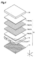
最初に、一実施形態のバックライト装置10の構造について、図1〜図7を使用して説明する。バックライト装置10は、液晶パネル20とともに液晶ディスプレイを構成する構成部品であり、液晶パネル20の背面上に設けられている。画像を表示するために、液晶パネル20の背面に向けて光を出力することがバックライト装置10の役割である。
First, the structure of the
図1においては、画像の出力方向が上向きの方向であり、したがってバックライト装置10は液晶パネル20の下に示されている。以下においては、バックライト装置10の構造における構成部品の鉛直方向の関係を示すために、図1に従って「上側」、「上面」、「下側」、「底面」等の用語が使用される。加えて本明細書では、バックライト装置10の構造の説明において、「x軸」は長方形の液晶パネル20の一組の反対面に沿った方向であり、「y軸」は液晶パネル20の出力面に垂直な方向であり、かつ「z軸」は液晶パネル20の他の組の反対面に沿った方向である。
In FIG. 1, the image output direction is an upward direction, and therefore the
図1に示すように、バックライト装置10は、光源11、導光体12、2枚のプリズムフィルム13、反射フィルム14、及び2枚の拡散フィルム15を含む。以下においては、必要に応じ、2枚のプリズムフィルム13が下側プリズムフィルム13a及び上側プリズムフィルム13bとして区別され、かつ2枚の拡散フィルム15が下側拡散フィルム15a及び上側拡散フィルム15bとして区別される。これらの構成部品のうち、光源11を除く板状の部材が以下の順序で積層される:反射フィルム(反射板)14、導光体12、下側拡散フィルム15a、下側プリズムフィルム13a、上側プリズムフィルム13b、及び上側拡散フィルム15b。
As shown in FIG. 1, the
光源11は導光体12の側面に隣接するように配置され、したがって、このバックライト装置10はエッジ−リット型(サイド−リット型)の装置である。本実施形態においては、光源11が3つの発光ダイオード(LED)から構成されているが、発光ダイオード(LED)の数は特には限定されない。加えて、光源11は、冷陰極管あるいは同種の物といった異なる光源とすることができる。光源11は、導光体12の一方の側面上のみに配置することができ、あるいは導光体12の2つの反対側の側面上に配置することもできる。
The
導光体12は、光源11から入射する光を液晶パネル20に垂直な方向(y軸方向)に導くための板状の部材である。本明細書においては、導光体12のy−z平面に平行な断面の形状が長方形であるが、光源11からの距離に応じて部分的にあるいは一律に細くなるように断面がテーパ状の構造も可能である。
The
下側拡散フィルム15a及び上側拡散フィルム15bは、液晶パネル20の前側表面における輝度(明るさ)のむらや同種のものを除去するために設けられた板状の部材である。
The
2枚のプリズムフィルム13の両方とも、液晶パネル20の前側表面における輝度を増加させるために使用される板状部材である。プリズムフィルム13として使用することができる製品の実例には(3Mによって製造される)TBEFが含まれる。
Both of the two
プリズム状のパターン(以下「プリズムパターン」と呼ぶ)は、プリズムフィルム13のそれぞれの上面(第1面)の上に形成される。プリズムパターンは、複数のつぶれた三角形の柱が同一方向に配置されたパターンとして構成することができる。加えて、プリズムパターンは、直線的な稜線を挟む2つの斜面から形成された山状の突起が同一方向に配置されたパターンとして構成することができる。この他には、プリズムパターンは、同一方向に沿って延びる「V」形の溝が同一の方向に配置されたパターンとして構成することができる。
A prism-like pattern (hereinafter referred to as “prism pattern”) is formed on each upper surface (first surface) of the
液晶パネル20の側から見たときに、下側プリズムフィルム13a及び上側プリズムフィルム13bのプリズムパターンの稜線は、互いに垂直となるように重なり合う。
When viewed from the
加えて、反射型偏光フィルムを使用することができる。この反射型偏光フィルムは、液晶パネル20の前側表面における輝度を増加させるために使用される板状の部材である。反射型偏光フィルムとして使用することができる製品の実例には(3Mによって製造される)DBEFが含まれる。
In addition, a reflective polarizing film can be used. This reflective polarizing film is a plate-like member used for increasing the luminance on the front surface of the
反射フィルム14は、その上面が光を全反射する反射面である板状の部材である。したがって、この反射面はプリズムフィルム13の底面と(間接的に)反対側にある。反射フィルム14として使用することができる製品の実例には、銀反射板及びESR(3Mによって製造される)が含まれる。散乱パターンは反射面上に形成される。
The
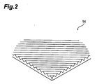
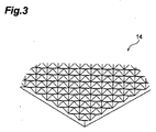
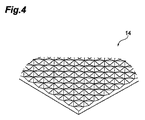
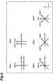
散乱パターンの実施例が図2〜図4に示されている。最初に、図2に示したように、散乱パターンは、プリズムフィルム13と同様のプリズムパターンとすることができ、そのような場合には散乱パターンの単位要素はプリズムである。加えて、散乱パターンは、ピラミッド状の突起が配置されたパターンとすることができる。図3に示した実施例においては、散乱パターンの単位要素が四角錐であるが、突起は三角錐あるいは同様なものといった異なる形状であってもよい。加えて、散乱パターンはピラミッド状の凹部が配置されたパターンとすることができる。図4に示した実施例においては、散乱パターンの単位要素が四角錐状の凹部であるが、凹部は三角錐あるいは同様のものといった異なる形状であってもよい。
Examples of scattering patterns are shown in FIGS. First, as shown in FIG. 2, the scattering pattern can be a prism pattern similar to the
したがって、散乱パターンは特定の形状には限定されない。しかしながら、散乱パターンを形成する斜面の少なくとも1つは、プリズムフィルム13のそれぞれのプリズムパターンを形成する斜面の方向を考慮に入れつつ形成されなければならない。具体的には、プリズムフィルム13のそれぞれのプリズムパターンを形成する斜面の第1の法線の軸線及び散乱パターンを形成する1つの斜面の第2の法線の軸線が、液晶パネル20に平行な仮想平面30上に投影されたときに、投影された2つの法線の軸線は鋭角をなさなければならない。本明細書においては、第1の法線の軸線及び第2の法線の軸線がなす角度は「バイアス」と呼ばれる。バイアス(鋭角)の最小値は、5度あるいは25度とすることができる。バイアスの最大値は65度あるいは85度とすることができる。液晶パネル20及びバックライト装置10を形成する板状の部材のそれぞれは実質的に平行であり、したがって、仮想平面30が板状の部材のそれぞれと平行な平面であることに留意されたい。
Therefore, the scattering pattern is not limited to a specific shape. However, at least one of the slopes that form the scattering pattern must be formed taking into account the direction of the slope that forms each prism pattern of the
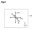
例えば、散乱パターンが図5の実施例に示されたプリズムパターンであるときには、図6に示したように、反射フィルム14の散乱パターンの法線の軸線42及び下側プリズムフィルム13aのプリズムパターンの法線の軸線41aがなす鋭角はθa度であり、かつ法線の軸線42及び上側プリズムフィルム13bのプリズムパターンの法線の軸線41bがなす鋭角はθb度である。
For example, when the scattering pattern is the prism pattern shown in the embodiment of FIG. 5, as shown in FIG. 6, the
図2及び図5に示されているプリズム状の散乱パターンにより、プリズムのうちの1つを形成する2つの斜面のそれぞれは、第2の法線の軸線及び第1の法線の軸線が鋭角をなすという関係を満たす。加えて、図3及び図4に示されている四角錐状の突起を形成する4つの斜面及び凹部は、第2の法線の軸線及び第1の法線の軸線が鋭角をなすという関係を満たす。もちろん、散乱パターンを形成する斜面の全てがこの関係を満たすことは必要ではない。様々な形態の散乱パターンを考え得るが、散乱パターンの単位要素の斜面の少なくとも1つが、第2の法線の軸線と第1の法線の軸線とが鋭角をなすという関係を満たせば十分である。 According to the prism-like scattering pattern shown in FIGS. 2 and 5, each of the two slopes forming one of the prisms has an acute angle between the axis of the second normal and the axis of the first normal. Satisfy the relationship of In addition, the four slopes and recesses forming the quadrangular pyramidal projections shown in FIGS. 3 and 4 have a relationship that the axis of the second normal and the axis of the first normal form an acute angle. Fulfill. Of course, it is not necessary that all of the slopes forming the scattering pattern satisfy this relationship. Although various forms of scattering patterns can be considered, it is sufficient if at least one of the slopes of the unit elements of the scattering pattern satisfies the relationship that the axis of the second normal and the axis of the first normal form an acute angle. is there.
図2〜図4に示されたような散乱パターンは、上述した銀反射板あるいはESRにホットプレス法あるいはフレームエンボシング法を施すことによって形成することができる。更にまた、マイクロ複製技術を使用して散乱パターンを形成した後、反射フィルム(反射板)は、銀あるいは同類のものといった金属をスパッタリング、蒸着あるいはメッキ法を使用してフィルム(プレート)の前側表面上にコーティングすることにより得ることができる。 The scattering pattern as shown in FIGS. 2 to 4 can be formed by subjecting the above-described silver reflector or ESR to hot pressing or frame embossing. Furthermore, after forming a scattering pattern using micro-replication technology, the reflective film (reflector) is a front surface of the film (plate) using sputtering, vapor deposition or plating methods such as silver or the like. It can be obtained by coating on top.
上述したように、この実施形態によると、プリズムフィルム13上のプリズムパターンの斜面と反射フィルム14上の散乱パターンの斜面との間の位置関係は、仮想平面30上に投影された第1の法線の軸線(例えば法線の軸線41a及び41b)と第2の法線の軸線(例えば法線の軸線42)とが鋭角をなすように設定される。この構造は、プリズムフィルム13から入射する光のより多くが、反復する全反射がプリズムフィルム13に生じない範囲で反射フィルム14において反射されることにつながる。このようにして反射された光の少なくとも一部は、プリズムフィルム13を透過して液晶パネル20に向かって進む。したがって、液晶パネル20により効率的に光を伝達することが可能である。
As described above, according to this embodiment, the positional relationship between the slope of the prism pattern on the
上述した効果を、図7を使用してより詳細に説明する。図7は、プリズムフィルム13と、散乱パターンのない平たんな反射面を有する反射板90との間での、光Lの再利用を示している。具体的には、光Lは、プリズムフィルム13と反射板90との間で全反射を繰り返しながら、板状の部材によって囲まれた空間の中でz軸に沿って(プリズムフィルム13のうちの1つのプリズム形状に沿って)進行する。光Lがx−y平面上に投影されたときに、光Lは、プリズムフィルム13と反射板90との間で実質的にy軸に沿って行ったり来たりするように見える。このプロセスは、プリズム形状について光の入射角が全反射の領域から外れるまで継続する。上述した現象は、x軸方向に沿って進む光(隣接するプリズムに移動しながら進む光)にも同様にあてはまる。
The effect mentioned above is demonstrated in detail using FIG. FIG. 7 shows the reuse of the light L between the
実際のシステムにおいては、導光体及び拡散フィルムにおける散乱により、光は、図7に示したシステムにおけるよりもいくらかより容易に全反射の領域から外れると考えられる。しかしながら、導光体及び拡散フィルムの拡散の度合いは低下する傾向にあり、したがって、プリズムフィルムと反射板との間で反復して行ったり来たりして進む光の経路を考慮することが重要である。 In an actual system, it is believed that due to scattering in the light guide and diffusing film, the light will deviate from the region of total reflection somewhat more easily than in the system shown in FIG. However, the degree of diffusion of the light guide and the diffusion film tends to decrease, so it is important to consider the path of light traveling back and forth between the prism film and the reflector. is there.
本実施形態において、散乱パターンは、反射フィルム14の反射面上に、従来技術の場合のように単純には形成されない。本実施形態においては、プリズムフィルム13から反射フィルム14への光の経路が考慮されるとともに、プリズムフィルム13上のプリズムパターンについての、反射フィルム14上の散乱パターンの斜面の位置が決定される。上述したように構成される斜面は、プリズムフィルム13から入射する光の反射方向を変更する。更に、反射方向が変更された入射光は多数の反復する再利用の経路(図7を参照)とは異なる経路に逃れ、したがって、入射光の一部はプリズムフィルム13において屈折し、液晶パネル20に向かって誘導される。したがって、光をより効率的に液晶パネル20に導くことが可能であり、その結果、液晶パネル20の輝度が高まる。
In the present embodiment, the scattering pattern is not simply formed on the reflective surface of the
しばらくの間、輝度レベルが増加した液晶パネルの要求があった。しかしながら、プリズムフィルムに使用する樹脂の屈折率を高める従来技術はその限界に近づいている。実際に、屈折率があるレベルを超えたときに輝度が減少することは知られている。したがって、使用する樹脂の屈折率を上げることによって液晶パネルの輝度を高める技術に取って代わる技術が望まれてきており、本実施形態はそのような必要性に応える。加えて、本実施形態によって、光は液晶パネルに効率的に伝達され、したがって液晶ディスプレイのエネルギー使用量を減少することもまた可能である。 There has been a demand for liquid crystal panels with increased brightness levels for some time. However, the prior art for increasing the refractive index of the resin used for the prism film is approaching its limit. In fact, it is known that the brightness decreases when the refractive index exceeds a certain level. Therefore, a technique that replaces the technique of increasing the luminance of the liquid crystal panel by increasing the refractive index of the resin used has been desired, and this embodiment meets such a need. In addition, this embodiment also allows light to be efficiently transmitted to the liquid crystal panel, thus reducing the energy usage of the liquid crystal display.
以下、本発明の一態様のバックライト装置を実施例に基づいて詳細に説明するが、バックライト装置の構造はこれらの実施例には限定されない。 Hereinafter, a backlight device of one embodiment of the present invention will be described in detail based on examples. However, the structure of the backlight device is not limited to these examples.
(実施例1)
バックライト装置の性能は、ソフトウェアLightTools(登録商標)バージョン6.3.0を使用するコンピュータシミュレーションにより評価された。バックライト装置モデルの属性は以下の通りに設定された。
寸法:45mm×30mm
タイプ:エッジ−リット装置
導光体の構造:その底面に球形の光抽出部を有する導光体
光源:2つのLED
2枚のプリズムフィルム:3Mによって製造されたTBEF 2−GT(24);プリズムピッチ=24μm。以下、必要に応じて、2枚のプリズムフィルムを「TBEF1」及び「TBEF2」として区別する。
反射フィルム:その反射面上に形成されたプリズムパターンを有する、3Mによって製造されたESR;プリズムピッチ=50μm。
拡散フィルム:なし
Example 1
The performance of the backlight device was evaluated by computer simulation using the software LightTools® version 6.3.0. The attributes of the backlight device model were set as follows.
Dimensions: 45mm x 30mm
Type: Edge-lit device Light guide structure: Light guide having a spherical light extraction part on its bottom surface Light source: Two LEDs
Two prism films: TBEF 2-GT manufactured by 3M (24); prism pitch = 24 μm. Hereinafter, the two prism films are distinguished as “TBEF1” and “TBEF2” as necessary.
Reflective film: ESR manufactured by 3M with a prism pattern formed on its reflective surface; prism pitch = 50 μm.
Diffusion film: None
上述した通りに構成されたバックライト装置モデル及び実施形態に説明したような仮想平面30が図8に示されている。3次元座標(x軸、y軸及びz軸)は、実施形態で説明したように構成された。
FIG. 8 shows the backlight device model configured as described above and the
図9に示すように、2枚のプリズムフィルム(TBEF)のプリズムパターンを形成する斜面の法線(第1の法線)と、反射フィルム(ESR)のプリズムパターンを形成する斜面の法線(第2の法線)との間の相対位置関係の、5つのバリエーションが構成された。図9は、仮想平面30(x−z平面)上に投影されたTBEF1及びTBEF2の法線及びESRの法線を示している。 As shown in FIG. 9, the slope normal line (first normal line) forming the prism pattern of the two prism films (TBEF) and the slope normal line forming the prism pattern of the reflective film (ESR) ( Five variations of the relative positional relationship with the second normal) were constructed. FIG. 9 shows the normal lines of TBEF1 and TBEF2 and the normal lines of ESR projected on the virtual plane 30 (xz plane).
TBEF1及びTBEF2の法線について、ケース1〜3においては、TBEF1の投影された法線がx軸に平行であり、かつTBEF2の投影された法線がz軸に平行であった。他方、ケース4及び5において、TBEF1及びTBEF2の投影された法線は、それぞれx軸に対し45度及び135度傾いていた。
Regarding the normals of TBEF1 and TBEF2, in cases 1 to 3, the projected normal of TBEF1 was parallel to the x-axis, and the projected normal of TBEF2 was parallel to the z-axis. On the other hand, in
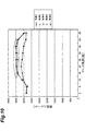
TBEF1、TBEF2の法線とESRの法線との間の関係について、ケース1及び2においては、ESRの投影された法線はTBEF1及びTBEF2の投影された法線のうちの1つに対し平行であり、したがって、バイアスは0度(又は90度)であった。これに対し、ケース3〜5においては、TBEF1及びTBEF 2のバイアスは45度であった。したがって、ケース1及び2は比較例とみなすことができ、かつケース3〜5は実施例とみなすことができる。上述した通りに構成されたケース1〜5のそれぞれにおいて、ESRの二等辺三角形の断面を有する各プリズムのベース角度を0から45度の範囲において1回につき5度ずつ変化させながら、バックライト装置の性能を評価した。バックライト装置の性能は、上側TBEFの上面上に配置された仮想輝度計を使用して測定された輝度により評価された。 Regarding the relationship between the normals of TBEF1, TBEF2 and the normals of ESR, in cases 1 and 2, the projected normal of ESR is parallel to one of the projected normals of TBEF1 and TBEF2. Therefore, the bias was 0 degrees (or 90 degrees). On the other hand, in cases 3 to 5, the biases of TBEF1 and TBEF2 were 45 degrees. Therefore, cases 1 and 2 can be regarded as comparative examples, and cases 3 to 5 can be regarded as examples. In each of the cases 1 to 5 configured as described above, the backlight device changes the base angle of each prism having an isosceles triangular section of ESR by 5 degrees at a time in the range of 0 to 45 degrees. The performance of was evaluated. The performance of the backlight device was evaluated by the luminance measured using a virtual luminance meter placed on the upper surface of the upper TBEF.
シミュレーション結果は図10のグラフに示されている。計算された輝度(cd/m2)がグラフの縦軸に示され、かつESRのプリズムベース角度(度)が横軸に示されている。 The simulation results are shown in the graph of FIG. The calculated luminance (cd / m 2 ) is shown on the vertical axis of the graph, and the prism base angle (degrees) of ESR is shown on the horizontal axis.
(実施例2)
バックライト装置モデルは実験例1(図8を参照)のように構成された。7つのケースが設定され、二等辺三角形の断面を有するESRの各プリズムのベース角度は、それぞれ10,15,20,25,30,35及び40度であった。続いて、ESRとTBEF(TBEF1及びTBEF2)のうちの1つによって形成されるバイアスを0から90度の範囲で1回につき5度ずつ変化させてバックライトの性能を評価した。輝度の測定点は、実施例1と同じであった。
(Example 2)
The backlight device model was configured as in Experimental Example 1 (see FIG. 8). Seven cases were set, and the base angles of each prism of the ESR having an isosceles triangular cross section were 10, 15, 20, 25, 30, 35, and 40 degrees, respectively. Subsequently, the performance of the backlight was evaluated by changing the bias formed by one of ESR and TBEF (TBEF1 and TBEF2) by 5 degrees at a time in the range of 0 to 90 degrees. The luminance measurement points were the same as in Example 1.
シミュレーションの結果が図11のグラフに示されている。計算された輝度(cd/m2)がグラフの縦軸に示され、かつバイアス(度)が横軸に示されている。 The result of the simulation is shown in the graph of FIG. The calculated luminance (cd / m 2 ) is shown on the vertical axis of the graph and the bias (degrees) is shown on the horizontal axis.
本発明を実施形態に基づいて詳細に説明してきた。しかしながら、本発明は上述した実施形態には限定されない。本発明には、その範囲から外れることなしに様々な修正をなすことができる。 The present invention has been described in detail based on the embodiments. However, the present invention is not limited to the embodiment described above. Various modifications can be made to the present invention without departing from the scope thereof.
例えば、実施形態においては、バックライト装置10が2枚のプリズムフィルム13を含んだが、1枚のプリズムフィルムのみを使用することもできる。加えて、実施形態においては、バックライト装置10が2枚の拡散フィルム15を含んだが、1枚の拡散フィルムのみを使用しあるいは拡散フィルムを全く使用しないこともできる。
For example, in the embodiment, the
実施形態において、バックライト装置10が液晶ディスプレイの構成部品として説明されたが、本発明の一態様のバックライト装置を適用できる表示装置(表示パネル)のタイプは液晶ディスプレイ(液晶パネル)には限定されない。
Although the
実施形態において、バックライト装置10はエッジライト装置であったが、本発明の一態様は様々なタイプのバックライトに適用することができる。例えば、本発明の一態様は、導光体が設けられていない直下型方式のバックライトに適用することができる。
In the embodiment, the
参照符号リスト
10 バックライト装置
11 光源
12 導光体
13 プリズムフィルム
13a 下側プリズムフィルム
13b 上側プリズムフィルム
14 反射フィルム(反射板)
15 拡散フィルム
15a 下側拡散フィルム
15b 上側拡散フィルム
20 液晶パネル(表示パネル)
30 仮想平面
41a及び41b 第1の法線の軸線
42 第2の法線の軸線
15
30
Claims (8)
前記表示パネルの側の第1面及び前記第1の面に反対側に第2面を有し、前記第1面上にプリズム状パターンが形成されているプリズムフィルムと、
前記第2面に対向する反射面を有し、前記反射面上に散乱パターンが形成されている反射板と、を含み、
前記プリズム状パターンを形成する斜面の第1の法線の軸線及び前記散乱パターンを形成する1つの斜面の第2の法線の軸線が前記表示パネルと平行な仮想平面上に投影されたときに、投影された前記第1及び前記第2の法線の軸線が鋭角をなす、バックライト装置。 A backlight device in which light emitted from a light source is output toward the back of the display panel,
A prism film having a first surface on the side of the display panel and a second surface on the opposite side to the first surface, wherein a prismatic pattern is formed on the first surface;
A reflective plate having a reflective surface facing the second surface, wherein a scattering pattern is formed on the reflective surface,
When the axis of the first normal line of the slope forming the prism-like pattern and the axis of the second normal line of one slope forming the scattering pattern are projected on a virtual plane parallel to the display panel The backlight device, wherein the projected first and second normal axes form an acute angle.
前記光源は、前記導光体の側面に隣接するように設けられる、請求項1〜6のいずれか一項に記載のバックライト装置。 A light guide provided between the prism film and the reflecting plate so as to extend along the reflecting surface;
The backlight device according to claim 1, wherein the light source is provided adjacent to a side surface of the light guide.
前記複数のプリズムフィルムのそれぞれが、前記投影された第1及び第2の法線の軸線が鋭角をなす関係を満たす、請求項1〜7のいずれか一項に記載のバックライト装置。 Including a plurality of prism films,
The backlight device according to claim 1, wherein each of the plurality of prism films satisfies a relationship in which an axis of the projected first and second normals forms an acute angle.
Priority Applications (1)
| Application Number | Priority Date | Filing Date | Title |
|---|---|---|---|
| JP2014530432A JP2014530455A (en) | 2011-09-20 | 2012-09-19 | Backlight device |
Applications Claiming Priority (3)
| Application Number | Priority Date | Filing Date | Title |
|---|---|---|---|
| JP2011204800 | 2011-09-20 | ||
| JP2011204800 | 2011-09-20 | ||
| JP2014530432A JP2014530455A (en) | 2011-09-20 | 2012-09-19 | Backlight device |
Publications (2)
| Publication Number | Publication Date |
|---|---|
| JP2014530455A true JP2014530455A (en) | 2014-11-17 |
| JP2014530455A5 JP2014530455A5 (en) | 2015-11-12 |
Family
ID=47003167
Family Applications (1)
| Application Number | Title | Priority Date | Filing Date |
|---|---|---|---|
| JP2014530432A Pending JP2014530455A (en) | 2011-09-20 | 2012-09-19 | Backlight device |
Country Status (8)
| Country | Link |
|---|---|
| US (1) | US9423553B2 (en) |
| EP (1) | EP2758831B1 (en) |
| JP (1) | JP2014530455A (en) |
| KR (1) | KR20140066237A (en) |
| CN (1) | CN103797406B (en) |
| SG (1) | SG11201400772WA (en) |
| TW (1) | TW201319645A (en) |
| WO (1) | WO2013042796A1 (en) |
Cited By (2)
| Publication number | Priority date | Publication date | Assignee | Title |
|---|---|---|---|---|
| JP2017092029A (en) * | 2015-11-05 | 2017-05-25 | 三星電子株式会社Samsung Electronics Co.,Ltd. | Light guide plate and backlighting device including the same |
| TWI657277B (en) * | 2018-03-06 | 2019-04-21 | 友達光電股份有限公司 | Display device |
Families Citing this family (5)
| Publication number | Priority date | Publication date | Assignee | Title |
|---|---|---|---|---|
| CN107505794B (en) * | 2017-09-28 | 2020-07-21 | 京东方科技集团股份有限公司 | Display device and backlight source |
| CN108279526A (en) * | 2017-12-28 | 2018-07-13 | 重庆市中光电显示技术有限公司 | Sidelight type backlight module |
| CN108679573A (en) * | 2018-05-31 | 2018-10-19 | 华域视觉科技(上海)有限公司 | LED light source face illuminating module and apply its car light |
| JP2023008355A (en) * | 2021-07-06 | 2023-01-19 | 恵和株式会社 | Optical sheet laminate, backlight unit, liquid crystal display device, information device, and method of manufacturing backlight unit |
| JP2023008354A (en) * | 2021-07-06 | 2023-01-19 | 恵和株式会社 | Optical sheet laminate, backlight unit, liquid crystal display device, information device, and method of manufacturing backlight unit |
Citations (5)
| Publication number | Priority date | Publication date | Assignee | Title |
|---|---|---|---|---|
| JPH08248233A (en) * | 1995-03-08 | 1996-09-27 | Nitto Jushi Kogyo Kk | Surface light source device and liquid crystal display |
| JP2000214460A (en) * | 1999-01-25 | 2000-08-04 | Sharp Corp | Back light device |
| WO2006134919A1 (en) * | 2005-06-13 | 2006-12-21 | Tsujiden Co., Ltd. | Reflection sheet |
| JP2007115451A (en) * | 2005-10-18 | 2007-05-10 | Omron Corp | Planar light source device |
| JP2010262813A (en) * | 2009-05-01 | 2010-11-18 | Hitachi Displays Ltd | Lighting device, and liquid crystal display device |
Family Cites Families (14)
| Publication number | Priority date | Publication date | Assignee | Title |
|---|---|---|---|---|
| US5359691A (en) * | 1992-10-08 | 1994-10-25 | Briteview Technologies | Backlighting system with a multi-reflection light injection system and using microprisms |
| JPH0794008A (en) | 1993-09-24 | 1995-04-07 | Chiyatani Sangyo Kk | Flat lighting device |
| JP2002124116A (en) | 2000-08-08 | 2002-04-26 | Yuka Denshi Co Ltd | Flat light source device, and a liquid crystal display device using the same |
| JP3871913B2 (en) * | 2000-11-14 | 2007-01-24 | シャープ株式会社 | Reflective display device and prism array sheet |
| KR100638658B1 (en) | 2004-10-20 | 2006-10-30 | 삼성전기주식회사 | Backlight apparatus |
| JP2006120975A (en) | 2004-10-25 | 2006-05-11 | Matsushita Electric Ind Co Ltd | Electronic component mounting device and holding tool |
| JP4672006B2 (en) * | 2005-03-01 | 2011-04-20 | シャープ株式会社 | Backlight unit and liquid crystal display device |
| KR20070077285A (en) * | 2006-01-23 | 2007-07-26 | 삼성전자주식회사 | Backlight assembly and display device having the same |
| CN101008683A (en) * | 2006-01-25 | 2007-08-01 | 扬明光学股份有限公司 | Brightening piece and back light module |
| JP2007220447A (en) | 2006-02-16 | 2007-08-30 | Harison Toshiba Lighting Corp | Sidelight type backlight apparatus |
| JP4853784B2 (en) | 2007-01-12 | 2012-01-11 | ミネベア株式会社 | Surface lighting device |
| CN101688991A (en) * | 2007-06-22 | 2010-03-31 | 3M创新有限公司 | Systems and methods for controlling backlight output characteristics |
| CN101910921A (en) | 2007-12-20 | 2010-12-08 | 3M创新有限公司 | Backlight reflectors with prism structure |
| CN102227587A (en) * | 2008-11-27 | 2011-10-26 | 夏普株式会社 | Planar light source device |
-
2012
- 2012-09-19 KR KR1020147010093A patent/KR20140066237A/en not_active Application Discontinuation
- 2012-09-19 US US14/346,233 patent/US9423553B2/en not_active Expired - Fee Related
- 2012-09-19 CN CN201280045252.5A patent/CN103797406B/en not_active Expired - Fee Related
- 2012-09-19 JP JP2014530432A patent/JP2014530455A/en active Pending
- 2012-09-19 WO PCT/JP2012/074607 patent/WO2013042796A1/en active Application Filing
- 2012-09-19 EP EP12769747.2A patent/EP2758831B1/en not_active Not-in-force
- 2012-09-19 SG SG11201400772WA patent/SG11201400772WA/en unknown
- 2012-09-20 TW TW101134533A patent/TW201319645A/en unknown
Patent Citations (7)
| Publication number | Priority date | Publication date | Assignee | Title |
|---|---|---|---|---|
| JPH08248233A (en) * | 1995-03-08 | 1996-09-27 | Nitto Jushi Kogyo Kk | Surface light source device and liquid crystal display |
| US5966192A (en) * | 1995-03-08 | 1999-10-12 | Nitto Jushi Kogyo Kabushiki Kaisha | Surface light source device and a liquid crystal display |
| JP2000214460A (en) * | 1999-01-25 | 2000-08-04 | Sharp Corp | Back light device |
| WO2006134919A1 (en) * | 2005-06-13 | 2006-12-21 | Tsujiden Co., Ltd. | Reflection sheet |
| US20090290098A1 (en) * | 2005-06-13 | 2009-11-26 | Tsujiden Co., Ltd. | Reflection sheet for backlight of liquid crystal display device, and backlight of liquid crystal display device using the reflection sheet |
| JP2007115451A (en) * | 2005-10-18 | 2007-05-10 | Omron Corp | Planar light source device |
| JP2010262813A (en) * | 2009-05-01 | 2010-11-18 | Hitachi Displays Ltd | Lighting device, and liquid crystal display device |
Cited By (2)
| Publication number | Priority date | Publication date | Assignee | Title |
|---|---|---|---|---|
| JP2017092029A (en) * | 2015-11-05 | 2017-05-25 | 三星電子株式会社Samsung Electronics Co.,Ltd. | Light guide plate and backlighting device including the same |
| TWI657277B (en) * | 2018-03-06 | 2019-04-21 | 友達光電股份有限公司 | Display device |
Also Published As
| Publication number | Publication date |
|---|---|
| EP2758831B1 (en) | 2017-05-17 |
| US20150177444A1 (en) | 2015-06-25 |
| SG11201400772WA (en) | 2014-04-28 |
| CN103797406B (en) | 2016-08-17 |
| TW201319645A (en) | 2013-05-16 |
| WO2013042796A1 (en) | 2013-03-28 |
| CN103797406A (en) | 2014-05-14 |
| EP2758831A1 (en) | 2014-07-30 |
| KR20140066237A (en) | 2014-05-30 |
| US9423553B2 (en) | 2016-08-23 |
Similar Documents
| Publication | Publication Date | Title |
|---|---|---|
| JP2014530455A (en) | Backlight device | |
| JP4282660B2 (en) | Prism sheet and backlight unit using the same | |
| JP5193987B2 (en) | Light guide plate and backlight module | |
| US20050002174A1 (en) | Light guide panel with optical deflector and edge-light type backlight system | |
| US20110176089A1 (en) | Area light source device and liquid crystal display device | |
| US20040207775A1 (en) | Light guide panel of edge-light type backlight system and edge-light type backlight system employing the same | |
| KR20090108588A (en) | Light outcoupling structure for a lighting device | |
| JP5199830B2 (en) | Display device | |
| US8287172B2 (en) | Planar illumination device | |
| US7753543B2 (en) | Prism sheet and backlight module using the same | |
| KR20160072049A (en) | Complex optical sheet, liquid crystal display using the same and method of manufacturing the same | |
| JP2013120394A (en) | Multilayer optical sheet module | |
| JP2015118906A (en) | Light guide plate and backlight unit | |
| TW201400765A (en) | Illumination device | |
| US10126483B2 (en) | Light guide plate assembly and display apparatus | |
| US7712945B2 (en) | Prism sheet and backlight module using the same | |
| JP4140016B2 (en) | Surface light emitting device, optical element, and liquid crystal display device | |
| JP5683917B2 (en) | Backlight module and optical panel thereof | |
| CN113227846B (en) | Light control film with turning film and lenticular diffuser for visual enhancement in horizontal plane | |
| JP3215902U (en) | Optical film and display device | |
| CN111929945B (en) | Collimating device, optical film, backlight module and display device | |
| KR101268074B1 (en) | Multilayer optical sheet module | |
| JP2006261107A (en) | Lighting system and display device using it | |
| JP6110826B2 (en) | Prism sheet, surface light source device, video source unit, and liquid crystal display device | |
| JP5363541B2 (en) | Light guide plate unit |
Legal Events
| Date | Code | Title | Description |
|---|---|---|---|
| A521 | Written amendment |
Free format text: JAPANESE INTERMEDIATE CODE: A523 Effective date: 20150924 |
|
| A621 | Written request for application examination |
Free format text: JAPANESE INTERMEDIATE CODE: A621 Effective date: 20150924 |
|
| A977 | Report on retrieval |
Free format text: JAPANESE INTERMEDIATE CODE: A971007 Effective date: 20160817 |
|
| A131 | Notification of reasons for refusal |
Free format text: JAPANESE INTERMEDIATE CODE: A131 Effective date: 20160823 |
|
| A601 | Written request for extension of time |
Free format text: JAPANESE INTERMEDIATE CODE: A601 Effective date: 20161124 |
|
| A02 | Decision of refusal |
Free format text: JAPANESE INTERMEDIATE CODE: A02 Effective date: 20170404 |