JP5199830B2 - Display device - Google Patents
Display device Download PDFInfo
- Publication number
- JP5199830B2 JP5199830B2 JP2008280630A JP2008280630A JP5199830B2 JP 5199830 B2 JP5199830 B2 JP 5199830B2 JP 2008280630 A JP2008280630 A JP 2008280630A JP 2008280630 A JP2008280630 A JP 2008280630A JP 5199830 B2 JP5199830 B2 JP 5199830B2
- Authority
- JP
- Japan
- Prior art keywords
- light
- light source
- microprism
- guide plate
- microprisms
- Prior art date
- Legal status (The legal status is an assumption and is not a legal conclusion. Google has not performed a legal analysis and makes no representation as to the accuracy of the status listed.)
- Expired - Fee Related
Links
Images


Classifications
-
- G—PHYSICS
- G02—OPTICS
- G02B—OPTICAL ELEMENTS, SYSTEMS OR APPARATUS
- G02B6/00—Light guides; Structural details of arrangements comprising light guides and other optical elements, e.g. couplings
- G02B6/0001—Light guides; Structural details of arrangements comprising light guides and other optical elements, e.g. couplings specially adapted for lighting devices or systems
- G02B6/0011—Light guides; Structural details of arrangements comprising light guides and other optical elements, e.g. couplings specially adapted for lighting devices or systems the light guides being planar or of plate-like form
- G02B6/0033—Means for improving the coupling-out of light from the light guide
- G02B6/0035—Means for improving the coupling-out of light from the light guide provided on the surface of the light guide or in the bulk of it
- G02B6/0036—2-D arrangement of prisms, protrusions, indentations or roughened surfaces
-
- G—PHYSICS
- G02—OPTICS
- G02B—OPTICAL ELEMENTS, SYSTEMS OR APPARATUS
- G02B6/00—Light guides; Structural details of arrangements comprising light guides and other optical elements, e.g. couplings
- G02B6/0001—Light guides; Structural details of arrangements comprising light guides and other optical elements, e.g. couplings specially adapted for lighting devices or systems
- G02B6/0011—Light guides; Structural details of arrangements comprising light guides and other optical elements, e.g. couplings specially adapted for lighting devices or systems the light guides being planar or of plate-like form
- G02B6/0013—Means for improving the coupling-in of light from the light source into the light guide
- G02B6/0015—Means for improving the coupling-in of light from the light source into the light guide provided on the surface of the light guide or in the bulk of it
- G02B6/002—Means for improving the coupling-in of light from the light source into the light guide provided on the surface of the light guide or in the bulk of it by shaping at least a portion of the light guide, e.g. with collimating, focussing or diverging surfaces
- G02B6/0021—Means for improving the coupling-in of light from the light source into the light guide provided on the surface of the light guide or in the bulk of it by shaping at least a portion of the light guide, e.g. with collimating, focussing or diverging surfaces for housing at least a part of the light source, e.g. by forming holes or recesses
Description
本発明は、携帯電話やモバイルコンピュータなどの携帯情報機器に用いられる表示装置に関する。 The present invention relates to a display device used in a portable information device such as a mobile phone or a mobile computer.
従来、携帯電話やモバイルコンピュータなどの携帯情報機器に用いられるカラー画像表示装置としては、小型薄型で低消費電力の液晶表示装置が多用されている。 2. Description of the Related Art Conventionally, as color image display devices used for portable information devices such as mobile phones and mobile computers, liquid crystal display devices that are small and thin and have low power consumption have been widely used.
液晶表示装置は光源としてバックライトを備えている。バックライトの種類としては、光源からの光を導光体の側面から入射して、導光板の上面(以下、出射面と称す)から出射させる、エッジライト方式の照明装置が知られている。光源には冷陰極管や発光ダイオード(LED)等の点光源を用い、導光板の出射面とは反対側の面(以下、対向面と称す)には、多数の溝部やドットパターンが形成されている。また、出射面には光を拡散させる効果をもつ拡散パターンが形成されていることが多い。導光体の入射面(すなわち、光源と対向して、光源の光が入射する面)にはプリズムが形成されており、点光源を拡散して面光源化する機能を持つ。この導光板の材料として、空気よりも屈折率の高いポリカーボネート(PC)やアクリル(PMMA)などの透明樹脂が使用される。また、導光体の出射面側には拡散シートやプリズムシートが配置されるような構成が主流である。さらに、導光体の下部には反射シートが配置される。 The liquid crystal display device includes a backlight as a light source. As a type of backlight, an edge light type illumination device is known in which light from a light source is incident from a side surface of a light guide and is emitted from an upper surface (hereinafter referred to as an emission surface) of a light guide plate. A point light source such as a cold-cathode tube or a light emitting diode (LED) is used as the light source, and a large number of grooves and dot patterns are formed on the surface opposite to the exit surface of the light guide plate (hereinafter referred to as the facing surface). ing. In addition, a diffusion pattern having an effect of diffusing light is often formed on the exit surface. A prism is formed on an incident surface of the light guide (that is, a surface on which light from the light source is incident facing the light source), and has a function of diffusing a point light source to form a surface light source. As a material for the light guide plate, a transparent resin such as polycarbonate (PC) or acrylic (PMMA) having a higher refractive index than air is used. In addition, a configuration in which a diffusion sheet and a prism sheet are arranged on the light exit surface side of the light guide is the mainstream. Further, a reflection sheet is disposed below the light guide.
また、LED等の点光源に特化し、かつプリズムシートがなくても機能するように、マイクロプリズムアレイを使用した導光板の開発も進んでいる。(例えば特許文献1)
従来のバックライトの構成では、プリズムシートを使用するため厚み、輝度効率、コスト、の限界が生じていた。特許文献1により提案されているマイクロプリズムアレイ方式のバックライトの場合、四角錘形拡散パターンが基本的に同じ方向を向いているため、点光源の光を十分活用しているとは言いがたい。輝度効率において、プリズムシートを使用した場合と比較して、ほぼ同等程度のレベルであり、バックライトの光源からの光の利用効率の非常に低い照明装置となってしまう。
In the conventional backlight configuration, a prism sheet is used, and thus there are limitations on thickness, luminance efficiency, and cost. In the case of the microprism array type backlight proposed in
更に、従来のマイクロプリズムアレイ方式の場合、ひとつの点光源にしか対応しておらず、光源を二つ以上に増やすことができなかった。 Furthermore, in the case of the conventional microprism array system, only one point light source is supported, and the number of light sources cannot be increased to two or more.
また、プリズムシートを使用しない構成の場合、液晶パネルを載せた場合に、モワレ(干渉)が発生しやすいという課題がある。 Further, in the case of a configuration that does not use a prism sheet, there is a problem that moire (interference) is likely to occur when a liquid crystal panel is mounted.
上記課題を解決するため、本発明の照明装置および表示装置は、光源と、光源からの光が入射する入射面と、照明光を出射する出射面と、出射面の反対側の対向面とを有する導光体を備える照明装置とこの照明装置の出射面上に表示素子を備える表示装置であって、対向面上にピラミッド形状のマイクロプリズムを液晶パネルの開口部と重なるエリアに最低でも2個以上配置した。また、入射面には半円形状の凹部からなる入光部が設けられており、入光部からの光を高効率で出射できるように、マイクロプリズムの配置角度を最適化した。 In order to solve the above problems, an illumination device and a display device according to the present invention include a light source, an incident surface on which light from the light source is incident, an exit surface that emits illumination light, and an opposing surface opposite to the exit surface. And a display device having a display element on an exit surface of the illumination device, wherein at least two pyramid-shaped microprisms on an opposing surface overlap an opening of a liquid crystal panel. Arranged above. Further, the incident surface is provided with a light incident portion including a semicircular concave portion, and the arrangement angle of the microprism is optimized so that light from the light incident portion can be emitted with high efficiency.
本発明によって、光源の光利用効率が非常に高く安価で薄型な照明装置が実現でき、かつ液晶パネルと組み合わせた場合に、モワレが発生しない表示装置を実現できた。また、複数の光源に対応することが可能となった。 According to the present invention, it is possible to realize an inexpensive and thin lighting device with very high light use efficiency of a light source, and a display device that does not cause moire when combined with a liquid crystal panel. Moreover, it became possible to deal with a plurality of light sources.
点光源と導光板を用いた照明装置において、導光板の対向面に複数の正四角錘のマイクロプリズムを形成し、光源とマイクロプリズムを結んだ直線を光路とした場合に、この光路に対してマイクロプリズムの鏡面の底辺が90度の角度になるようにマイクロプリズムを配置した。このような構成により、光源から導光板に入射した光がマイクロプリズムにあたって導光板の出光面からの出射する際に、光の利用効率を最もあげることができる。マイクロプリズムは導光板の対向面に凹形状で形成され、高さが1〜10μm、低角が40〜50度であることが望ましい。 In a lighting device using a point light source and a light guide plate, when a plurality of square prism microprisms are formed on the opposite surface of the light guide plate and a straight line connecting the light source and the microprism is used as the optical path, The microprism was arranged so that the bottom of the mirror surface of the microprism was at an angle of 90 degrees. With such a configuration, when the light incident on the light guide plate from the light source exits from the light exit surface of the light guide plate on the microprism, the light utilization efficiency can be maximized. The microprism is preferably formed in a concave shape on the opposite surface of the light guide plate, and has a height of 1 to 10 μm and a low angle of 40 to 50 degrees.
さらに、導光板の出射面に入射面と垂直になるように縦プリズムを形成することで、プリズムシートを利用することなく、照明装置の輝線を消すことができる。また、ブラスト工法等で出射面を部分的もしくは全面を荒らしたり、印刷工法等で拡散層を形成したりしても縦プリズムと同様に輝線軽減の効果が得られる。 Furthermore, by forming a vertical prism on the light exit surface of the light guide plate so as to be perpendicular to the light entrance surface, the bright line of the illumination device can be eliminated without using a prism sheet. Even if the exit surface is partially or entirely roughened by a blasting method or the like, or a diffusion layer is formed by a printing method or the like, the effect of reducing bright lines can be obtained as in the case of the vertical prism.
また、入射面に光源に対応した半円形状の凹部からなる入光部を設け、マイクロプリズムを鏡面の底辺が入光部からの光の光路に対して垂直になるように配置した。このように配置することにより、入光部の形状によって光の光路が異なってもマイクロプリズムの鏡面に光源からの光を垂直に照射することができ、光の利用効率を最もあげることができる。 In addition, a light incident portion made of a semicircular concave portion corresponding to the light source is provided on the incident surface, and the microprism is arranged so that the bottom side of the mirror surface is perpendicular to the light path of the light from the light incident portion. By arranging in this way, the light from the light source can be vertically irradiated onto the mirror surface of the microprism even if the optical path of the light varies depending on the shape of the light incident portion, and the light utilization efficiency can be maximized.
また、光源を複数設け、これらのいずれかの光源からの光路に対して鏡面が垂直になるようにマイクロプリズムを配置した。 Also, a plurality of light sources are provided, and the microprisms are arranged so that the mirror surfaces are perpendicular to the optical path from any one of these light sources.
また、本発明の照明装置の出射面の上方に配置され、照明装置により照明される表示素子を備える表示装置において、照明光を通過させる領域を表示素子の開口部とした場合に、マイクロプリズムのピッチを表示素子の開口部のピッチと同等、もしくは1/3以下になるように配置した。このようにピッチをマトリックスで配列することにより、表示素子の各開口部、つまり液晶パネルの各ドットピッチに対応するマイクロプリズムの数の差をなくし、液晶パネルのドット間の輝度差を解消してモワレや干渉縞を防止することができる。 Further, in a display device including a display element that is disposed above the emission surface of the illumination device of the present invention and is illuminated by the illumination device, when the region through which illumination light passes is an opening of the display element, The pitch was arranged so as to be equal to or less than 1/3 of the pitch of the openings of the display element. This arrangement of pitches in a matrix eliminates the difference in the number of microprisms corresponding to each opening of the display element, that is, each dot pitch of the liquid crystal panel, and eliminates the luminance difference between the dots of the liquid crystal panel. Moire and interference fringes can be prevented.
以下に本発明の表示装置に関して、図面を用いて具体的に説明する。 The display device of the present invention will be specifically described below with reference to the drawings.
本実施例の表示装置を図1から図5を用いて説明する。 The display device of this embodiment will be described with reference to FIGS.
図1に本実施例の照明装置の正面構成を模式的に示す。本実施例ではバックライトの光源1として白色LEDパッケージを用いている。白色LEDパッケージは青色LEDに黄色の蛍光体をポッティングしたタイプである。光源1の前方に、光源1から出射した光を導光する導光板2が配置されている。本実施例では、光源1は点光源であり、サイドビュータイプの白色LEDを想定しているが、トップビューでも砲弾型でも白色以外の色であってもかまわない。導光板2はゼオノア、PMMA、PC等の透明樹脂の成形品である。光源1からの光は、透明な導光板2の内部を伝播して、上表面である光出射面から表示素子に照射される。導光板2の入射面に対向して光源1が配置されている。
FIG. 1 schematically shows a front configuration of the illumination apparatus according to the present embodiment. In this embodiment, a white LED package is used as the
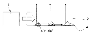
導光板2の光出射面と反対の対向面側に無数のマイクロプリズム4が配置されている。マイクロプリズム4は正四角錐のピラミッド形状になっており、光源1からの光を反射する鏡面を備えている。本発明の実施例においては正四角錘の4つの側面のうち、光源1からの光を反射する面を鏡面とする。マイクロプリズム4は正面から見ると鏡面の向きが場所によって異なるように配置されている。マイクロプリズム4の鏡面の底辺は、光源1とそれぞれのマイクロプリズム4を結ぶ直線を光路3とすると、光路3に対して、おおよそ90度になるように配置されている。そのように配置することで、光源1から入射した光がマイクロプリズム4にあたって導光板出光面から出射する際に光の利用効率を最も高くすることができる。
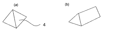
図2にマイクロプリズム4の斜視構成を示す。(a)が本発明のマイクロプリズム4である。図示するようにマイクロプリズム4は正四角錐であり、高さは1〜10μm程度である。底辺と頂点を結ぶ直線と底面の角度は40〜60度程度である。(b)は従来技術の一例であるが、長方形を底面とする五面体である。(b)のような形状では、パターンを小さくすることが難しい。射出成形でマイクロプリズムを形成する場合、小さくても1μm程度が限界である。(a)のような正四角錐形状とすることによって、パターンを小さくすることができるため、設計の自由度が広がり、後述するモワレ対策等の実施が容易となる。
FIG. 2 shows a perspective configuration of the
図3に本実施例の照明装置の断面図を示す。光源1からの光は導光板2に入射し、マイクロプリズム4の鏡面に当たって出射面から出射する。マイクロプリズム4は導光板2の対向面に対して凹パターンで形成される。マイクロプリズム4に当たった光は、その全てが鏡面で反射して出射面から出射するわけではなく、一部の光はマイクロプリズム4を透過して鏡面の対向面にあたり、屈折しながら再度導光板2に入射する。その際に鏡面の対向面と底面とが形成する角度が鏡面と底面が形成する角度と同じになることが好ましい。本実施例では、マイクロプリズムが正四角錐であるため、鏡面と底面、また鏡面の対向面が形成する角度は同じとなり、おおよそ45度である。
FIG. 3 shows a cross-sectional view of the illumination device of this embodiment. Light from the
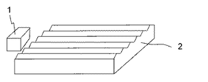
図4に本実施例による照明装置の斜視構成を模式的に示す。光源1から導光板2に入射した光は、導光板2内部を導波し、前述のマイクロプリズム4の鏡面で反射されて出射する。この出射面には複数の縦プリズムが導光板2の長手方向に平行に形成されている。縦プリズムは導光板2の入射面に対して垂直に形成されている。縦プリズムの頂角の角度は120〜170度程度である。モワレ防止のためピッチは細かいほど好ましいが、製法の限界上15〜100μm程度となる。本発明のようにプリズムシートを使用しない構成のバックライトでは、光源1から直線状にどの角度からも見える光線と呼ばれる現象が発生しやすい。縦プリズムを配置することで、輝線の発生を軽減することが可能である。また、縦プリズムではなく、ブラスト工法等で出射面を部分的もしくは全面を荒らしたり、印刷工法等で拡散層を形成したりしても縦プリズムと同様に輝線軽減の効果が得られる。
FIG. 4 schematically shows a perspective configuration of the lighting apparatus according to the present embodiment. Light incident on the
図5に本実施例の表示装置の斜視構成を模式的に示す。図示するように、液晶パネル16は、ガラス基板5aと対向基板5bの間隙に液晶層8が封入された構成である。ガラス基板5aには下ITO7aとTFTエリア6が形成されており、その上に更に下配向膜9aが形成されている。一方、対向する対向基板5b上には赤色カラーフィルター10Rと緑色カラーフィルター10Gと青色カラーフィルター10Bが形成されている。これらカラーフィルター層の間隙にはブラックマトリックス11が形成されている。赤色カラーフィルター10Rと緑色カラーフィルター10Gと青色カラーフィルター10Bとブラックマトリックス11の形成領域は、平坦化層14によって平坦化されている。平坦化層14の上には、下ITO7aに対向して画素電極を形成する上ITO7bが設けられている。そして、これらの上ITO7bの上にも上配向膜9bが形成されている。このような表面構造のガラス基板5aと対向基板5bは、成膜面が向き合うようにしてスペーサ12を介して所定の間隙で接合されている。図示されていないが、この間隙を形成するために、スペーサの内部や、基板間に所定の粒径を持ったビーズを散布する場合が多い。そして、この基板間隙に液晶層8が封入されている。この液晶層8の液晶分子の初期配向は、上下配向膜9a、9bによって規制されている。ガラス基板5a上には下偏光板4a,対向基板5b上には上偏光板4bが配置されている。液晶パネル13の画素領域には、ブラックマトリックス11とTFTエリア6と重なる表示の無効な領域と、表示の有効な領域が設けられており、本発明では、この表示の有効な領域を開口部とする。なお、この開口部は液晶パネル13上の各ドットに対応している。
FIG. 5 schematically shows a perspective configuration of the display device of this embodiment. As shown in the drawing, the
各開口部は、マイクロプリズム4によって反射された光源1からの光によって照明される。そのため、各開口部に対応するマイクロプリズムの数に差が生じると、液晶パネルのドット間の輝度差が発生する。この輝度差は開口部のピッチ(液晶パネルのドットピッチ)と導光板2の隣接するマイクロプリズム4の配列ピッチが異なることからも生じる。この輝度差が著しいと、モワレや干渉縞と呼ばれる現象が発生する。そのため、各開口部に対応するマイクロプリズムの数を同等にすることが望ましい。また、隣接するマイクロプリズム4の中心のピッチを液晶パネル16のドットピッチとまったく同じ、もしくは液晶パネル16のドットピッチの1/3以下としてもよい。このような配列をマトリックスで実施することで、液晶パネルのドット間の輝度差を緩和しモワレの発生を防止することができる。
Each opening is illuminated with light from the
さらに、光拡散シートを導光板と液晶素子の間に設けてもよい。光拡散シートは表面に微細な凹凸形状が形成されたり、ビーズが塗布されたりしており、これによって光を拡散する作用を備えている。 Further, a light diffusion sheet may be provided between the light guide plate and the liquid crystal element. The light diffusing sheet has a fine irregular shape formed on the surface or coated with beads, thereby diffusing light.
図6に本実施例における導光板2を模式的に示す正面図を記す。実施例1と異なる点は、導光板2の入光部の形状である。導光板2の入射面に光源1に対応するように半円状の凹部を設けており、この凹部が入光部となる。本実施例のように入光部が半円形状の凹部の場合、光源1からの光は半円形状の入光部で屈折して導光板2へ入射するため、光路が実施例1と異なる。従って、マイクロプリズム4の最適な配置が実施例1とは異なってくる。
FIG. 6 is a front view schematically showing the
(a)の入光部は、半円の先端を尖らせたような形状で、(b)の入光部は半円の先端をへこませたような形状となっている。光路3aおよび光路3bはそれぞれ入光部から垂直に延ばした直線である。(a)と(b)では入光部の半円形状が異なり光の屈折率が違うため、光路3aと光路3bでは、光の方向が異なる。(a)と(b)の導光板2にはマイクロプリズム4がそれぞれ同じ配列で配置されている。(b)と比較すると(a)の方が光源1からの光がより多くのプリズム4の鏡面にあたっている。このように入光部の形状により光源からの光の方向が変わるため、導光板2のマイクロプリズムの配置はマイクロプリズム4の鏡面に光源1からの光があたるように変える必要がある。(a)の場合は光路3aに対して、(b)の場合は光路3bに対して鏡面の底辺が90度になるようにマイクロプリズム4を配置すると光の利用効率を最も上げることができる。つまり、本実施例のように入光部が半円形状の場合は、入光部の半円から垂直に延ばした直線を光路とすると、光路に対して、マイクロプリズムの鏡面の底辺がおおよそ90度になるようにマイクロプリズム4を配置する。
The light incident part in (a) has a shape that sharpens the tip of a semicircle, and the light incident part in (b) has a shape that has a dented tip of a semicircle. Each of the
図7に本実施例における導光板2を模式的に示す正面図を記す。実施例1、及び2と異なる点は、光源1の数量とマイクロプリズム4の配置方法である。本実施例では、導光板2の入射面に対して、光源1cと光源1dが配置してある。導光板2上にはマイクロプリズム4c及び、4dが配置されている。マイクロプリズム4cとマイクロプリズム4dはそれぞれ光源1cと光源1dに対応したマイクロプリズムである。マイクロプリズム4cと4dは交互に配列されている。光源1cとマイクロプリズム4cを結んだ光路3cに対してマイクロプリズム4cの鏡面の底辺がおおよそ90度になるように配置した。また、光源1dとマイクロプリズム4dを結んだ光路3dに対してマイクロプリズム4dの鏡面の底辺がおおよそ90度になるように配置した。このようにマイクロプリズムを配置することにより、光源からの光の利用効率を高めることができる。本実施例では、光源の数は2つであるが、3つ以上の場合においてもそれぞれの光源に対応するマイクロプリズムを、各光路に対して鏡面の底辺がおおよそ90度になるように配置すれば本実施例と同等の機能を発揮する。
FIG. 7 is a front view schematically showing the
1 光源
2 導光板
3 光路
4 マイクロプリズム
5a ガラス基板
5b 対向基板
6 TFTエリア
7a 下ITO
7b 上ITO
8 液晶層
9配光膜
10R 赤色カラーフィルター
10G 緑色カラーフィルター
10B 青色カラーフィルター
11 ブラックマトリックス
12 スペーサ
13a 下偏光板
13b 上偏光板
14 平坦化層
15 反射シート
16 液晶パネル
DESCRIPTION OF
7b Top ITO
8 Liquid crystal layer 9
Claims (2)
前記対向面に形成された複数のマイクロプリズムと、
前記凹部に配置された光源と、
前記出射面の上方に配置され、前記照明光により照明される表示素子と、を備え、
前記マイクロプリズムは正四角錘の形状であり、該正四角錘の一つの側面が前記光源からの光を前記出射面に向けて反射する鏡面であり、
前記鏡面の底辺が、前記凹部から入射した前記光源の光の光路に対して垂直であり、
前記表示素子は前記照明光を通過させる複数の開口部を有し、
前記マイクロプリズムは、前記開口部のそれぞれに対応してマトリックス状に配列され、
前記開口部のそれぞれに対応する前記マイクロプリズムの数が同等であることを特徴とする表示装置。 A light guide plate having an incident surface on which light is incident, an exit surface from which illumination light exits, a facing surface opposite to the exit surface, and a semicircular recess formed in the incident surface;
A plurality of microprisms formed on the facing surface;
A light source disposed in the recess;
A display element disposed above the exit surface and illuminated by the illumination light,
The microprism has a shape of a regular square pyramid, and one side surface of the regular square pyramid is a mirror surface that reflects light from the light source toward the emission surface,
Bottom of the mirror surface state, and are perpendicular to the optical path of the light of the light source incident from the concave portion,
The display element has a plurality of openings through which the illumination light passes.
The microprisms are arranged in a matrix corresponding to each of the openings,
A display device, wherein the number of the microprisms corresponding to each of the openings is equal .
Priority Applications (2)
| Application Number | Priority Date | Filing Date | Title |
|---|---|---|---|
| JP2008280630A JP5199830B2 (en) | 2008-10-31 | 2008-10-31 | Display device |
| US12/589,918 US8251565B2 (en) | 2008-10-31 | 2009-10-30 | Illumination device and display device |
Applications Claiming Priority (1)
| Application Number | Priority Date | Filing Date | Title |
|---|---|---|---|
| JP2008280630A JP5199830B2 (en) | 2008-10-31 | 2008-10-31 | Display device |
Publications (3)
| Publication Number | Publication Date |
|---|---|
| JP2010108795A JP2010108795A (en) | 2010-05-13 |
| JP2010108795A5 JP2010108795A5 (en) | 2011-09-15 |
| JP5199830B2 true JP5199830B2 (en) | 2013-05-15 |
Family
ID=42171936
Family Applications (1)
| Application Number | Title | Priority Date | Filing Date |
|---|---|---|---|
| JP2008280630A Expired - Fee Related JP5199830B2 (en) | 2008-10-31 | 2008-10-31 | Display device |
Country Status (2)
| Country | Link |
|---|---|
| US (1) | US8251565B2 (en) |
| JP (1) | JP5199830B2 (en) |
Families Citing this family (12)
| Publication number | Priority date | Publication date | Assignee | Title |
|---|---|---|---|---|
| WO2011071257A2 (en) * | 2009-12-08 | 2011-06-16 | Lg Electronics Inc. | Display apparatus |
| JP2012079681A (en) * | 2010-09-09 | 2012-04-19 | Hitachi Chemical Co Ltd | Light guide plate and surface light source device |
| US20130182200A1 (en) * | 2010-10-08 | 2013-07-18 | Sharp Kabushiki Kaisha | Light guide plate, illumination device, and liquid crystal display device |
| US20120170310A1 (en) * | 2011-01-05 | 2012-07-05 | Qualcomm Mems Technologies, Inc. | Light guide with uniform light distribution |
| KR101481677B1 (en) | 2012-11-30 | 2015-01-13 | 엘지디스플레이 주식회사 | Back Light Unit and Liquid Crystal Display device Comprising The Same And Fabricating Method thereof |
| CN104360431B (en) * | 2014-11-26 | 2017-03-08 | 深圳市华星光电技术有限公司 | Light guide plate, backlight module and display |
| JP6561644B2 (en) * | 2014-12-25 | 2019-08-21 | オムロン株式会社 | Light guide plate, display device and game machine |
| WO2016103865A1 (en) * | 2014-12-25 | 2016-06-30 | オムロン株式会社 | Light guide plate, display device, and game machine |
| FR3032512B1 (en) * | 2015-02-05 | 2020-01-17 | Valeo Vision | LIGHT GUIDE WITH MEANS OF COMPENSATING FOR PROGRESSIVE LOSS OF LIGHT ALONG THE GUIDE |
| KR102435848B1 (en) * | 2015-03-31 | 2022-08-24 | 서울반도체 주식회사 | Light device of vehicle |
| EP3076069B1 (en) | 2015-03-31 | 2020-03-11 | Seoul Semiconductor Co., Ltd. | Light device of vehicle |
| JP6786822B2 (en) * | 2016-03-14 | 2020-11-18 | オムロン株式会社 | Display device and game machine |
Family Cites Families (12)
| Publication number | Priority date | Publication date | Assignee | Title |
|---|---|---|---|---|
| GB1439027A (en) * | 1973-07-18 | 1976-06-09 | Fibreglass Ltd | Manufacture of glass wool |
| DE69217177T2 (en) * | 1991-11-28 | 1997-05-15 | Enplas Corp | Flat light source |
| US5695269A (en) * | 1996-01-29 | 1997-12-09 | Delco Electronics Corporation | Multi-color display lighting by led |
| TW592308U (en) * | 1999-02-17 | 2004-06-11 | Enplas Corp | Light guiding plate, surface light source device, and liquid crystal display device |
| JP3434465B2 (en) * | 1999-04-22 | 2003-08-11 | 三菱電機株式会社 | Backlight for liquid crystal display |
| JP4242090B2 (en) * | 2000-11-08 | 2009-03-18 | 三菱レイヨン株式会社 | Surface light source device |
| KR100765138B1 (en) * | 2001-04-09 | 2007-10-15 | 삼성전자주식회사 | Backlight assembly and liquid crystal display device using thereof |
| JP3828402B2 (en) * | 2001-11-08 | 2006-10-04 | 株式会社日立製作所 | BACKLIGHTING DEVICE, LIQUID CRYSTAL DISPLAY DEVICE USING SAME, AND LIGHTING METHOD FOR LIQUID CRYSTAL DISPLAY DEVICE |
| TWI247142B (en) * | 2002-11-20 | 2006-01-11 | Hon Hai Prec Ind Co Ltd | Light guide plate used for backlight module |
| TW200722852A (en) * | 2005-12-06 | 2007-06-16 | Nano Prec Corp | Edge-type backlight module |
| JP4694985B2 (en) * | 2006-02-13 | 2011-06-08 | セイコーインスツル株式会社 | Surface light emitting device and display device |
| KR100771828B1 (en) * | 2006-04-04 | 2007-10-30 | 삼성전기주식회사 | Light Guide Plate and Liquid Crystal Display Device having its |
-
2008
- 2008-10-31 JP JP2008280630A patent/JP5199830B2/en not_active Expired - Fee Related
-
2009
- 2009-10-30 US US12/589,918 patent/US8251565B2/en active Active
Also Published As
| Publication number | Publication date |
|---|---|
| JP2010108795A (en) | 2010-05-13 |
| US20100124076A1 (en) | 2010-05-20 |
| US8251565B2 (en) | 2012-08-28 |
Similar Documents
| Publication | Publication Date | Title |
|---|---|---|
| JP5199830B2 (en) | Display device | |
| US8388207B2 (en) | Illuminating device and display device having the same | |
| KR101391891B1 (en) | Light guide plate, manufacturing method thereof and liquid crystal display including the same | |
| JP4282660B2 (en) | Prism sheet and backlight unit using the same | |
| KR100978078B1 (en) | Prism sheet and liquid crystal display having the same | |
| KR100898100B1 (en) | Prism sheet | |
| TWI425262B (en) | Local dimming side-lighting light guide plate and local dimming side-lighting backlight module using the same | |
| KR20030096509A (en) | Prism sheet and lcd having the same | |
| JP2004126016A (en) | Optical film, diffusion sheet, reflection plate, surface light source device, and liquid crystal display device | |
| KR20100066001A (en) | Display device | |
| US9022635B2 (en) | Light guide plate and backlight unit | |
| KR20130000252A (en) | Light guide plate for backlight unit and manufacturing method thereof | |
| US10324249B2 (en) | Display device | |
| US20220113591A1 (en) | Diffusion plate and backlight module | |
| US10534126B2 (en) | Lighting device and display device | |
| WO2017170017A1 (en) | Illumination device and display device | |
| JP2007200736A (en) | Lighting system, electrooptical device and electronic equipment | |
| KR20060088923A (en) | Back light assembly and liquid crystal display apparatus having the same | |
| JP2009157074A (en) | Beam control unit | |
| JPH1172787A (en) | Illumination device, liquid crystal display device and electronic equipment | |
| KR102030412B1 (en) | Light guide plate having rounded polyggon pattern and liquid cyrstal display device having thereof | |
| US20080130318A1 (en) | Backlight unit | |
| JP6682834B2 (en) | Light guide plate, surface light source device, display device, and electronic device | |
| JP5184240B2 (en) | Display device | |
| KR20120039405A (en) | Backlight unit and liquid crystal display device having the same |
Legal Events
| Date | Code | Title | Description |
|---|---|---|---|
| A521 | Written amendment |
Free format text: JAPANESE INTERMEDIATE CODE: A523 Effective date: 20110803 |
|
| A621 | Written request for application examination |
Free format text: JAPANESE INTERMEDIATE CODE: A621 Effective date: 20110803 |
|
| A131 | Notification of reasons for refusal |
Free format text: JAPANESE INTERMEDIATE CODE: A131 Effective date: 20121106 |
|
| A521 | Written amendment |
Free format text: JAPANESE INTERMEDIATE CODE: A523 Effective date: 20121217 |
|
| TRDD | Decision of grant or rejection written | ||
| A01 | Written decision to grant a patent or to grant a registration (utility model) |
Free format text: JAPANESE INTERMEDIATE CODE: A01 Effective date: 20130205 |
|
| A61 | First payment of annual fees (during grant procedure) |
Free format text: JAPANESE INTERMEDIATE CODE: A61 Effective date: 20130208 |
|
| FPAY | Renewal fee payment (event date is renewal date of database) |
Free format text: PAYMENT UNTIL: 20160215 Year of fee payment: 3 |
|
| R150 | Certificate of patent or registration of utility model |
Ref document number: 5199830 Country of ref document: JP Free format text: JAPANESE INTERMEDIATE CODE: R150 Free format text: JAPANESE INTERMEDIATE CODE: R150 |
|
| R250 | Receipt of annual fees |
Free format text: JAPANESE INTERMEDIATE CODE: R250 |
|
| R250 | Receipt of annual fees |
Free format text: JAPANESE INTERMEDIATE CODE: R250 |
|
| R250 | Receipt of annual fees |
Free format text: JAPANESE INTERMEDIATE CODE: R250 |
|
| R250 | Receipt of annual fees |
Free format text: JAPANESE INTERMEDIATE CODE: R250 |
|
| LAPS | Cancellation because of no payment of annual fees |