JP2014515537A - Apparatus and method for providing data integrity - Google Patents
Apparatus and method for providing data integrity Download PDFInfo
- Publication number
- JP2014515537A JP2014515537A JP2014513641A JP2014513641A JP2014515537A JP 2014515537 A JP2014515537 A JP 2014515537A JP 2014513641 A JP2014513641 A JP 2014513641A JP 2014513641 A JP2014513641 A JP 2014513641A JP 2014515537 A JP2014515537 A JP 2014515537A
- Authority
- JP
- Japan
- Prior art keywords
- data
- error
- memory
- metadata
- integrity
- Prior art date
- Legal status (The legal status is an assumption and is not a legal conclusion. Google has not performed a legal analysis and makes no representation as to the accuracy of the status listed.)
- Pending
Links
- 238000000034 method Methods 0.000 title claims abstract description 31
- 230000015654 memory Effects 0.000 claims abstract description 108
- 238000012937 correction Methods 0.000 claims description 21
- 238000011084 recovery Methods 0.000 claims description 14
- 230000004044 response Effects 0.000 claims description 14
- 238000012360 testing method Methods 0.000 claims description 10
- 238000004519 manufacturing process Methods 0.000 claims description 4
- 230000000977 initiatory effect Effects 0.000 claims 3
- 238000007726 management method Methods 0.000 description 31
- 238000012546 transfer Methods 0.000 description 15
- 230000006870 function Effects 0.000 description 9
- 238000001514 detection method Methods 0.000 description 8
- 238000010586 diagram Methods 0.000 description 8
- 230000008859 change Effects 0.000 description 6
- 230000008569 process Effects 0.000 description 5
- 238000003491 array Methods 0.000 description 4
- 230000008901 benefit Effects 0.000 description 4
- 239000004065 semiconductor Substances 0.000 description 4
- 239000007787 solid Substances 0.000 description 4
- 238000006243 chemical reaction Methods 0.000 description 3
- 238000012545 processing Methods 0.000 description 3
- 238000013403 standard screening design Methods 0.000 description 3
- 238000003860 storage Methods 0.000 description 3
- 230000007717 exclusion Effects 0.000 description 2
- 230000002093 peripheral effect Effects 0.000 description 2
- 230000009467 reduction Effects 0.000 description 2
- 206010009944 Colon cancer Diseases 0.000 description 1
- 230000006978 adaptation Effects 0.000 description 1
- 230000009286 beneficial effect Effects 0.000 description 1
- 239000003990 capacitor Substances 0.000 description 1
- 238000004891 communication Methods 0.000 description 1
- 125000004122 cyclic group Chemical group 0.000 description 1
- 238000013500 data storage Methods 0.000 description 1
- 230000001934 delay Effects 0.000 description 1
- 230000000694 effects Effects 0.000 description 1
- 238000005516 engineering process Methods 0.000 description 1
- 238000007667 floating Methods 0.000 description 1
- 238000003780 insertion Methods 0.000 description 1
- 230000037431 insertion Effects 0.000 description 1
- 238000007689 inspection Methods 0.000 description 1
- 238000012986 modification Methods 0.000 description 1
- 230000004048 modification Effects 0.000 description 1
- 150000004767 nitrides Chemical class 0.000 description 1
- 238000002360 preparation method Methods 0.000 description 1
- 238000012552 review Methods 0.000 description 1
- 230000001360 synchronised effect Effects 0.000 description 1
Images


Classifications
-
- G—PHYSICS
- G06—COMPUTING; CALCULATING OR COUNTING
- G06F—ELECTRIC DIGITAL DATA PROCESSING
- G06F11/00—Error detection; Error correction; Monitoring
- G06F11/07—Responding to the occurrence of a fault, e.g. fault tolerance
- G06F11/16—Error detection or correction of the data by redundancy in hardware
- G06F11/20—Error detection or correction of the data by redundancy in hardware using active fault-masking, e.g. by switching out faulty elements or by switching in spare elements
- G06F11/2053—Error detection or correction of the data by redundancy in hardware using active fault-masking, e.g. by switching out faulty elements or by switching in spare elements where persistent mass storage functionality or persistent mass storage control functionality is redundant
-
- G—PHYSICS
- G06—COMPUTING; CALCULATING OR COUNTING
- G06F—ELECTRIC DIGITAL DATA PROCESSING
- G06F11/00—Error detection; Error correction; Monitoring
- G06F11/07—Responding to the occurrence of a fault, e.g. fault tolerance
- G06F11/08—Error detection or correction by redundancy in data representation, e.g. by using checking codes
- G06F11/10—Adding special bits or symbols to the coded information, e.g. parity check, casting out 9's or 11's
- G06F11/1004—Adding special bits or symbols to the coded information, e.g. parity check, casting out 9's or 11's to protect a block of data words, e.g. CRC or checksum
-
- G—PHYSICS
- G06—COMPUTING; CALCULATING OR COUNTING
- G06F—ELECTRIC DIGITAL DATA PROCESSING
- G06F11/00—Error detection; Error correction; Monitoring
- G06F11/07—Responding to the occurrence of a fault, e.g. fault tolerance
- G06F11/0703—Error or fault processing not based on redundancy, i.e. by taking additional measures to deal with the error or fault not making use of redundancy in operation, in hardware, or in data representation
- G06F11/0706—Error or fault processing not based on redundancy, i.e. by taking additional measures to deal with the error or fault not making use of redundancy in operation, in hardware, or in data representation the processing taking place on a specific hardware platform or in a specific software environment
- G06F11/073—Error or fault processing not based on redundancy, i.e. by taking additional measures to deal with the error or fault not making use of redundancy in operation, in hardware, or in data representation the processing taking place on a specific hardware platform or in a specific software environment in a memory management context, e.g. virtual memory or cache management
-
- G—PHYSICS
- G06—COMPUTING; CALCULATING OR COUNTING
- G06F—ELECTRIC DIGITAL DATA PROCESSING
- G06F11/00—Error detection; Error correction; Monitoring
- G06F11/07—Responding to the occurrence of a fault, e.g. fault tolerance
- G06F11/0703—Error or fault processing not based on redundancy, i.e. by taking additional measures to deal with the error or fault not making use of redundancy in operation, in hardware, or in data representation
- G06F11/0751—Error or fault detection not based on redundancy
- G06F11/0754—Error or fault detection not based on redundancy by exceeding limits
- G06F11/076—Error or fault detection not based on redundancy by exceeding limits by exceeding a count or rate limit, e.g. word- or bit count limit
-
- G—PHYSICS
- G06—COMPUTING; CALCULATING OR COUNTING
- G06F—ELECTRIC DIGITAL DATA PROCESSING
- G06F11/00—Error detection; Error correction; Monitoring
- G06F11/07—Responding to the occurrence of a fault, e.g. fault tolerance
- G06F11/08—Error detection or correction by redundancy in data representation, e.g. by using checking codes
- G06F11/10—Adding special bits or symbols to the coded information, e.g. parity check, casting out 9's or 11's
- G06F11/1076—Parity data used in redundant arrays of independent storages, e.g. in RAID systems
- G06F11/1092—Rebuilding, e.g. when physically replacing a failing disk
-
- G—PHYSICS
- G06—COMPUTING; CALCULATING OR COUNTING
- G06F—ELECTRIC DIGITAL DATA PROCESSING
- G06F12/00—Accessing, addressing or allocating within memory systems or architectures
Landscapes
- Engineering & Computer Science (AREA)
- Theoretical Computer Science (AREA)
- General Engineering & Computer Science (AREA)
- Physics & Mathematics (AREA)
- General Physics & Mathematics (AREA)
- Quality & Reliability (AREA)
- Computer Security & Cryptography (AREA)
- Techniques For Improving Reliability Of Storages (AREA)
- Information Retrieval, Db Structures And Fs Structures Therefor (AREA)
Abstract
本開示は、データ完全性を与えるための装置(たとえばコンピューティングシステム、メモリシステム、コントローラなど)および方法を含む。1つまたは複数の方法には、たとえば、いくつかのメモリデバイスに書き込まれるデータのいくつかのセクターを受け取ること、およびそのいくつかのセクターに対応する第1のメタデータを付加するとともに、そのいくつかのセクターに第1の完全性データを含めることが含まれうる。この第1のメタデータは特定の形式を有するものである。当該方法にはさらに、第2のメタデータで与えられる第2の完全性データを生成することが含まれうる。この第2の完全性データはいくつかのセクターの中の少なくとも1つに対応するものである(第2のメタデータは第2の形式を有する)。当該方法にはさらに、第2のメタデータで与えられる第3の完全性データを生成することが含まれうる。この第3の完全性データは、第2の完全性データおよびいくつかのセクターの中の少なくとも1つに対応するエラーデータを含むものである。
【選択図】図6The present disclosure includes devices (eg, computing systems, memory systems, controllers, etc.) and methods for providing data integrity. One or more methods include, for example, receiving a number of sectors of data to be written to a number of memory devices, and adding first metadata corresponding to the number of sectors and a number of Including the first integrity data in the sector may be included. This first metadata has a specific format. The method can further include generating second integrity data provided in the second metadata. This second integrity data corresponds to at least one of several sectors (second metadata has a second format). The method can further include generating third integrity data provided in the second metadata. The third integrity data includes second integrity data and error data corresponding to at least one of the several sectors.
[Selection] Figure 6
Description
本開示は、概括的には半導体メモリデバイス、方法、およびシステムに関し、より具体的には、データ完全性を与えるための装置および方法に関する。 The present disclosure relates generally to semiconductor memory devices, methods, and systems, and more specifically to an apparatus and method for providing data integrity.
メモリデバイスは、典型的には、コンピュータ内の内部回路、半導体、集積回路またはその他の電子機器として提供される。揮発性メモリおよび不揮発性メモリを含む多くの異なる種類のメモリが存在する。揮発性メモリは、そのメモリのデータを保持するために電力を必要とする場合があり、たとえば、ランダムアクセスメモリ(RAM)、ダイナミックランダムアクセスメモリ(DRAM)、シンクロナスダイナミックランダムアクセスメモリ(SDRAM)などがこれに含まれる。不揮発性メモリは、無給電時に格納データを保持することによって永続的データを提供することができ、たとえば、NANDフラッシュメモリ、NORフラッシュメモリ、読み出し専用メモリ(ROM)、電気的に消去可能なプログラマブルROM(EEPROM)、消去可能なプログラマブルROM(EPROM)のほか、相変化ランダムアクセスメモリ(PCRAM)、抵抗変化ランダムアクセスメモリ(RRAM(登録商標))、磁気抵抗ランダムアクセスメモリ(MRAM)などの可変抵抗メモリがこれに含まれうる。 The memory device is typically provided as an internal circuit, semiconductor, integrated circuit or other electronic device in a computer. There are many different types of memory including volatile and non-volatile memory. Volatile memory may require power to hold data in the memory, for example, random access memory (RAM), dynamic random access memory (DRAM), synchronous dynamic random access memory (SDRAM), etc. This is included. Nonvolatile memory can provide permanent data by holding stored data when no power is supplied, for example, NAND flash memory, NOR flash memory, read only memory (ROM), electrically erasable programmable ROM (EEPROM), erasable programmable ROM (EPROM), variable resistance memory such as phase change random access memory (PCRAM), resistance change random access memory (RRAM (registered trademark)), magnetoresistive random access memory (MRAM) Can be included in this.
メモリデバイスを組み合わせ、ソリッドステートドライブ(SSD)などのメモリシステムのストレージボリュームを形成することができる。ソリッドステートドライブには、不揮発性メモリ(たとえばNANDフラッシュメモリおよびNORフラッシュメモリ)および/または揮発性メモリ(たとえばDRAMおよびSRAM)が含まれるほか、その他各種の不揮発性および揮発性メモリが含まれうる。フラッシュメモリデバイスには、データを窒化物層内の電荷トラップ内に格納する半導体−酸化物−窒化物−酸化物−半導体および金属−酸化物−窒化物−酸化物−半導体のコンデンサ構造を使用したフローティングゲートフラッシュデバイスおよびチャージトラップフラッシュ(CTF)デバイスが含まれ、これを広範な電子的用途のための不揮発性メモリとして利用することができる。フラッシュメモリデバイスは、典型的には、高メモリ密度、高信頼性、および低電力消費を実現可能な1トランジスタ型メモリセルを使用する。 Memory devices can be combined to form a storage volume of a memory system such as a solid state drive (SSD). Solid state drives include non-volatile memory (eg, NAND flash memory and NOR flash memory) and / or volatile memory (eg, DRAM and SRAM), as well as various other types of non-volatile and volatile memory. Flash memory devices used semiconductor-oxide-nitride-oxide-semiconductor and metal-oxide-nitride-oxide-semiconductor capacitor structures that store data in charge traps in the nitride layer. Floating gate flash devices and charge trap flash (CTF) devices are included and can be utilized as non-volatile memories for a wide range of electronic applications. Flash memory devices typically use one-transistor memory cells that can achieve high memory density, high reliability, and low power consumption.
SSDは、性能、サイズ、重量、耐久性、動作温度範囲、および電力消費に関してハードドライブに勝る利点を持ちうるため、コンピュータの主記憶装置としてハードディスクドライブを代替するために使用することができる。たとえば、SSDは、可動部品がないことにより、シークタイム、レイテンシーなど、磁気ディスクドライブに付随する電気機械的遅延を回避しうるため、磁気ディスクドライブと比較して、すぐれた性能を有することができる。SSD製造業者は、不揮発性フラッシュメモリを使用して内蔵電池供給が不要なフラッシュSSDを作製することができ、そのためドライブをより多用途かつ小型にすることが可能になる。 Because SSDs can have advantages over hard drives in terms of performance, size, weight, durability, operating temperature range, and power consumption, they can be used to replace hard disk drives as the computer's main storage. For example, SSDs can have superior performance compared to magnetic disk drives because no moving parts can avoid electro-mechanical delays associated with magnetic disk drives such as seek time and latency. . SSD manufacturers can use non-volatile flash memory to create flash SSDs that do not require a built-in battery supply, thus making the drive more versatile and smaller.
SSDには、いくつかのメモリデバイス(たとえばいくつかのメモリチップ)が含まれうる。メモリデバイスには、いくつかのダイおよび/または論理ユニット(LUN)が含まれうる。各ダイの面上にいくつかのメモリアレイおよび周辺回路を設けることができ、そのメモリアレイには、いくつかの物理ページに編成されたメモリセルのいくつかのブロックが含まれうる。 An SSD may include several memory devices (eg, several memory chips). A memory device may include several dies and / or logical units (LUNs). There can be several memory arrays and peripheral circuits on the surface of each die, which can include several blocks of memory cells organized into several physical pages.
SSDは、メモリデバイスとホスト間でデータ(たとえばユーザーデータおよびそれに関連するエラーデータ、アドレスデータなどの完全性データ)を転送するための、読み出しおよび書き込み動作などのメモリ動作に関連してホストからコマンドを受け取ることができる。たとえば転送中にデータが破壊されていないという確信を与えるために、それらの動作に関連してメモリデバイスとホストとの間で転送されるデータのエンド−エンド間の完全性を提供することが有益でありうる。 The SSD is a command from the host related to memory operations such as read and write operations to transfer data (eg, user data and associated error data, integrity data such as address data) between the memory device and the host. Can receive. It is beneficial to provide end-to-end integrity of the data transferred between the memory device and the host in connection with their operation, for example to give confidence that the data has not been corrupted during the transfer It can be.
本開示は、データ完全性を与えるための装置(たとえばコンピューティングシステム、メモリシステム、コントローラなど)および方法を含む。1つまたは複数の方法実施形態には、たとえば、いくつかのメモリデバイス(たとえば単一メモリデバイス)に書き込まれるデータのいくつかのセクターを受け取ることと、およびそのいくつかのセクターに対応する第1のメタデータを付加することと、そのいくつかのセクターに第1の完全性データを含めることとが含まれ、この第1のメタデータは特定の形式を有するものである。方法実施形態にはさらに、第2のメタデータで与えられる第2の完全性データを生成することが含まれ、この第2の完全性データはいくつかのセクターの中の少なくとも1つに対応するものである(第2のメタデータは第2の形式を有する)。方法実施形態にはさらに、第2のメタデータで与えられる第3の完全性データを生成することが含まれ、この第3の完全性データは、第2の完全性データおよびいくつかのセクターの中の少なくとも1つに対応するエラーデータを含むものである。 The present disclosure includes devices (eg, computing systems, memory systems, controllers, etc.) and methods for providing data integrity. One or more method embodiments include, for example, receiving a number of sectors of data to be written to a number of memory devices (eg, a single memory device) and a first corresponding to the number of sectors. And including first integrity data in some sectors, the first metadata having a specific format. The method embodiment further includes generating second integrity data provided in the second metadata, the second integrity data corresponding to at least one of the several sectors. (The second metadata has the second format). The method embodiment further includes generating third integrity data provided in the second metadata, wherein the third integrity data includes the second integrity data and the number of sectors. Error data corresponding to at least one of them is included.
本開示の1つまたは複数の実施形態は、たとえばメモリシステム内のエンド−エンド間のデータ完全性を与える柔軟なアーキテクチャを提供する。たとえば、1つまたは複数の実施形態は、メタデータ形式変換を実行することができ、これには、各種メモリデバイスと関連付けられた異なるページサイズおよび/または利用可能メタデータサイズに適合させることが可能になるなど、さまざまな利点がある。1つまたは複数の実施形態は、本明細書に説明する実施形態に従ってデータ完全性を維持しながらエラー回復動作を実行することができるコントローラを含み、これにより、実施されるデバイス製造試験(たとえば消費者に引き渡す前の現場での出荷前試験)の量の低減など、さまざまな利点が提供されうる。 One or more embodiments of the present disclosure provide a flexible architecture that provides end-to-end data integrity, eg, in a memory system. For example, one or more embodiments can perform metadata format conversion, which can be adapted to different page sizes and / or available metadata sizes associated with various memory devices. There are various advantages such as becoming. One or more embodiments include a controller that can perform error recovery operations while maintaining data integrity in accordance with the embodiments described herein, thereby performing device manufacturing tests (eg, consumption) performed. Various benefits can be provided, such as a reduced amount of on-site pre-shipment testing prior to delivery to the person.
本開示に関する以下の詳細な説明では、本明細書の一部を形成する添付の図面を参照する。各図面には、本開示の1つまたは複数の実施形態を実践することが可能な方法が例示されており、これらの実施形態は、本開示の実施形態を当業者が実践できるように十分な詳しさで説明されている。当然のことながら、その他の実施形態も利用可能であり、また、本開示の範囲から逸脱することなく、プロセスの変更、電気的および/または構造的変更を加えることができる。本明細書で使用される指示記号「N」は、とくに図面内の参照番号に関して、その記号によって指示されたいくつかの特定機能要素を本開示の1つまたは複数の実施形態に含めることができるということを示す。本明細書で使用される用語の「いくつかの(a number of)〜」は、1つまたは複数の対象物に言及することができる(たとえば、いくつかのメモリデバイスは1つまたは複数のメモリデバイスに言及しうる)。 In the following detailed description of the disclosure, reference is made to the accompanying drawings that form a part hereof. Each drawing illustrates how one or more embodiments of the present disclosure may be practiced, and these embodiments are sufficient to enable one of ordinary skill in the art to practice the embodiments of the present disclosure. It is explained in detail. Of course, other embodiments may be utilized and process changes, electrical and / or structural changes may be made without departing from the scope of the present disclosure. The designation symbol “N” as used herein may include several specific functional elements indicated by that symbol in one or more embodiments of the present disclosure, particularly with reference to reference numerals in the drawings. It shows that. As used herein, the term “a number of” may refer to one or more objects (eg, some memory devices may include one or more memories). May refer to the device).
本明細書の図は、先頭の数字(1桁または複数桁)が図面番号に対応し、残りの数字が図面内の要素または構成部分を識別するという付番規則に従っている。複数の図に含まれる類似の要素または構成部分は、同様の数字の使用によって識別されうる。たとえば、108は図1の要素「08」を参照し、図2では類似要素が208として参照されうる。当然ながら、本明細書中の各種の実施形態に示された要素を追加、交換および/または除去することにより、本開示のいくつかの付加的な実施形態が提供されうる。さらに当然のこととして、図中に示された各要素の比率および相対的な大きさは、本発明の実施形態を図示することを意図したものであり、限定の意味で解釈されるべきではない。 The figures in this specification follow a numbering rule in which the first digit (one or more digits) corresponds to a drawing number and the remaining digits identify an element or component in the drawing. Similar elements or components included in multiple figures may be identified by the use of similar numbers. For example, 108 may refer to element “08” in FIG. 1 and a similar element may be referred to as 208 in FIG. Of course, several additional embodiments of the present disclosure may be provided by adding, replacing, and / or removing elements shown in the various embodiments herein. Furthermore, it should be understood that the ratios and relative sizes of the elements shown in the figures are intended to illustrate embodiments of the invention and should not be construed in a limiting sense. .
図1は、本開示の1つまたは複数の実施形態による少なくとも1つのメモリシステム104を含むコンピューティングシステム100の機能ブロック図である。メモリシステム104は、たとえばソリッドステートドライブ(SSD)であってよく、物理ホストインタフェース106、メモリシステムコントローラ108(たとえばプロセッサおよび/またはその他の制御回路)、および1つまたは複数のメモリデバイス110−1〜110−N(たとえばNANDフラッシュデバイスなどのソリッドステートメモリデバイス)が含まれうる。これにより、メモリシステム104のストレージボリュームが提供される。
FIG. 1 is a functional block diagram of a
図1に示すように、物理ホストインタフェース106はコントローラ108に結合されており、メモリシステム104とホスト102との間でデータを通信するために使用することができる。インタフェース106は、標準化インタフェースの形であってよい。たとえば、メモリシステム104がコンピューティングシステム100内のデータストレージ用に使用される場合、物理ホストインタフェース106は、SATA(serial advanced technology attachment)、PCIe(peripheral component interconnect express)、ユニバーサルシリアルバス(USB)、またはその他各種のコネクタおよびインタフェースでありうる。しかし、一般に物理ホストインタフェース106は、メモリシステム104とホスト102との間で制御、アドレス、データ、およびその他の信号を受け渡しするためのインタフェースを提供することができ、ホスト102は物理ホストインタフェース106に対する適合レセプタを有する。
As shown in FIG. 1, the
ホスト102は、パーソナルラップトップコンピュータ、デスクトップコンピュータ、デジタルカメラ、携帯電話、またはメモリカードリーダーなどのホストシステムのほか、その他各種のホストでありうる。ホスト102は、システムマザーボードおよび/またはバックプレーンとともにメモリアクセスデバイス(たとえばいくつかのプロセッサ)を備えることができる。
The
コントローラ108は、データの読み出し、書き込み、消去などの各種動作を実行するために、メモリデバイス110−1〜110−Nと通信することができる。コントローラ108は、たとえば、いくつかのコンポーネント(たとえば1つまたは複数の集積回路)を含む回路および/またはファームウェアであってよい。たとえば、コントローラ108は、メモリデバイス110−1〜110−Nに対するアクセスを制御するための制御回路およびホスト102とメモリシステム104との間の変換層を与えるための回路を備えることができる。したがって、メモリコントローラ108は、適切な信号を適切な時間に適切なI/O接続で受け取るためにメモリデバイス110−1〜110−NのI/O接続(図1に図示せず)を選択的に結合することができる。同様に、ホスト102とメモリシステム104との間の通信プロトコルは、メモリデバイス110−1〜110−Nにアクセスするために使用されるプロトコルと異なるものであってよい。その場合、コントローラ108は、ホスト102から受け取ったコマンドを適切なコマンドに変換して、いくつかのメモリデバイス110−1〜110−Nに対する所望のアクセスを達成することができる。
The
メモリデバイス110−1〜110−Nには、メモリセル(たとえば不揮発性メモリセル)の1つまたは複数のアレイが含まれうる。それらのアレイは、たとえばNANDアーキテクチャを有するフラッシュアレイであってよい。しかし、実施形態は、特定の種類のメモリアレイまたはアレイアーキテクチャに限定されない。 Memory devices 110-1 through 110-N may include one or more arrays of memory cells (eg, non-volatile memory cells). These arrays may be flash arrays having, for example, a NAND architecture. However, embodiments are not limited to a particular type of memory array or array architecture.
メモリデバイス110−1〜110−Nには、たとえば、いくつかの物理ページを含むいくつかのブロックへのグループ化が可能ないくつかのメモリセルが含まれうる。メモリセルのプレーンにいくつかのブロックを含めることができ、1つのアレイにいくつかのプレーンが含まれうる。一例として、1つのメモリデバイスは、1ページ当たり4320バイト(B)のデータ、1ブロック当たり128ページ、1プレーン当たり2048ブロック、および1デバイス当たり16プレーンを含むことができる。 The memory devices 110-1 to 110-N may include several memory cells that can be grouped into several blocks including several physical pages, for example. Several blocks can be included in a plane of memory cells, and several planes can be included in one array. As an example, a memory device may include 4320 bytes (B) of data per page, 128 pages per block, 2048 blocks per plane, and 16 planes per device.
動作時には、メモリシステムのメモリデバイス(たとえばシステム104のメモリデバイス110−1〜110−N)に対し、1ページのデータとしてデータの書き込みおよび/または読み出しを実行することができる。そのような1ページのデータはメモリシステムのデータ転送サイズと呼ぶことができる。ホスト(たとえばホスト102)との間でデータをセクター単位で転送することができる。そのような1セクターのデータはホストのデータ転送サイズと呼ぶことができる。 In operation, data can be written and / or read as a page of data to memory devices of the memory system (eg, memory devices 110-1 to 110-N of system 104). Such a page of data can be referred to as the data transfer size of the memory system. Data can be transferred to / from a host (for example, the host 102) in units of sectors. Such data of one sector can be called a host data transfer size.
1ページのデータには、ユーザーデータのいくつかのバイト(たとえばデータのいくつかのセクターを含むデータペイロード)とともに、それに対応するメタデータが含まれうるが、多くの場合、1ページのデータのサイズによって表されるのは、ユーザーデータを格納するために使用されるバイト数のみである。一例として、4KBのページサイズを有する1ページのデータには、ユーザーデータを格納するために使用される4KB(たとえばセクターサイズを512Bと仮定して8セクター)とともに、そのユーザーデータに対応するメタデータを格納するためのいくつかのバイト(たとえば32B、54B、224Bなど)が含まれうる。そのメタデータには、エラーデータ(たとえばエラー検出および/または訂正コードデータ)などの完全性データおよび/またはアドレスデータ(たとえば論理アドレスデータ)のほか、ユーザーデータに対応する各種のメタデータを含めることができる。 A page of data can include several bytes of user data (eg, a data payload containing several sectors of data) and corresponding metadata, but in many cases the size of the data of one page Is represented only by the number of bytes used to store user data. As an example, a page of data having a page size of 4 KB includes 4 KB (for example, 8 sectors assuming a sector size of 512 B) used for storing user data, and metadata corresponding to the user data. Several bytes (e.g., 32B, 54B, 224B, etc.) may be included. The metadata includes integrity data such as error data (eg error detection and / or correction code data) and / or address data (eg logical address data) as well as various metadata corresponding to user data. Can do.
メモリデバイス(たとえばデバイス110−1〜110−N)の種類によって、提供されるページサイズが異なり、かつ/または格納ページに関連して利用可能なメタデータバイトの量が異なることがある。また、メモリデバイスの種類によってビットエラーレートが異なることがあり、その場合、データページの完全性を確保するために必要なメタデータの量が変化する場合がある(たとえば、ビットエラーレートがより高いメモリデバイスは、ビットエラーレートがより低いメモリデバイスと比較して、より多くのバイト数のエラー訂正コードデータを必要とすることがある)。一例として、マルチレベルセル(MLC)NANDフラッシュデバイスのビットエラーレートは、シングルレベルセル(SLC)NANDフラッシュデバイスよりも高くなる可能性がある。そのため、MLCデバイスは、エラーデータに関してSLCデバイスよりも多くのメタデータバイトを使用することがある。場合によっては、1ページのデータに関する所望の完全性を与えるために必要なメタデータの量が1つのメモリデバイスによって提供されるメタデータバイト数を超えることもある。すなわち、当該ページに対応する複数セクター(たとえばユーザーデータ)に関する十分なエンド−エンド間のデータ完全性を与えるために望ましい量よりも利用可能な量のメタデータバイトの方が少ないということが起こりうる。 Depending on the type of memory device (e.g., devices 110-1 through 110-N), the provided page size may vary and / or the amount of metadata bytes available in association with the stored page may vary. Also, the bit error rate may vary depending on the type of memory device, in which case the amount of metadata required to ensure the integrity of the data page may change (eg, higher bit error rate) Memory devices may require a greater number of bytes of error correction code data compared to memory devices with lower bit error rates). As an example, the bit error rate of a multi-level cell (MLC) NAND flash device can be higher than a single-level cell (SLC) NAND flash device. As such, the MLC device may use more metadata bytes than the SLC device for error data. In some cases, the amount of metadata required to provide the desired integrity for a page of data may exceed the number of metadata bytes provided by a memory device. That is, it may happen that there are fewer metadata bytes available than desired to provide sufficient end-to-end data integrity for multiple sectors (eg, user data) corresponding to the page. .
図2は、本開示の1つまたは複数の実施形態による転送データの完全性を与えることに関連したメモリコントローラ208の機能ブロック図である。コントローラ208は、図1に示したメモリシステム104などのメモリシステムのコンポーネントであってよい。当業者によって理解されるように、図2に示した以外の追加回路およびコンポーネントを設けることができ、また、図2は図示を容易にする目的で細部が簡略化されている。実施形態は図2に示した例に限定されない。たとえば、コントローラ208の1つまたは複数の例示コンポーネントを単一コンポーネントとして統合することができる。また、本開示のいくつかの実施形態において、1つまたは複数の例示コンポーネントを任意とすることができる。
FIG. 2 is a functional block diagram of the
図2に示すように、メモリコントローラ208は、ホストインタフェース206といくつかのメモリデバイス210との間でデータを転送するために使用される制御回路を備える。メモリデバイス210は、図1に示したメモリデバイス110−1〜110−Nなどのメモリデバイスであってよい。
As shown in FIG. 2, the
いくつかの実施形態において、制御回路は、ホストインタフェース206といくつかのメモリデバイス210との間で転送されるデータの完全性を与えるために、第1の形式と第2の形式との間でメタデータ形式を整合させる(たとえば変更する)ように構成される。一例として、第1のメタデータ形式には1セクター単位の完全性データが含まれ、第2のメタデータ形式には複数セクター単位の完全性データが含まれる。詳しくは後述するように、転送データの完全性を与えることには複数の処理が含まれうる。具体的には、第1の形式を有するメタデータである、ホストから(たとえばホストからの書き込み要求に関連して)受信したいくつかのセクター(たとえば図3に示すデータフィールド348に配置されたセクター)に対応するメタデータ(たとえば図3に示すメタデータ341)について、第1の完全性データ(たとえばエラーデータおよび/またはアドレスデータ)の検査を実行すること、および第2のメタデータ(たとえば図4に示すメタデータ447および/または図5に示すメタデータ547−0/547−1)に関する第2の完全性データ(たとえば図4に示す完全性データ454−0/454−1および/または図5に示す552/554)を生成することが含まれ、この第2の完全性データはいくつかのセクターの中の少なくとも1つに対応しており、上記の処理にはさらに、第2のメタデータに関する第3の完全性データ(たとえば図4に示す完全性データ458および/または図5に示す558−0/558−1)を生成することが含まれる。この第3の完全性データは、いくつかのセクターの中の少なくとも1つに対応するとともに第2の完全性データに対応するエラーデータを含む。
In some embodiments, the control circuit is between a first type and a second type to provide integrity of data transferred between the
コントローラ208は、(たとえばホストからの書き込み要求に応答して)ホストから受信したデータ(たとえばユーザーデータ)のいくつかのセクターを1つのページとして書き込むことができる。さまざまな例において、コントローラ208が受信するセクター数は、いくつかのメモリデバイス210のページサイズに対応するセクター数よりも少ない可能性がある。そのような場合、コントローラ208は、部分ページ書き込み動作を実行することができ、これには、たとえば、ホストから受信したセクターをメモリデバイス210から読み出したページのセクターと結合する(たとえば読み出したページのセクターをホストから受信したセクターに置き換える)ことによって結合ページを形成することと、それに続いて結合ページをメモリデバイス210に書き込むことが含まれうる。同様に、コントローラ208は、(たとえばメモリデバイス210のページサイズに対応するセクター数よりも少ないいくつかのセクターを対象としたホスト読み出し要求に応答して)部分ページ読み出し動作を実行することができる。部分ページ読み出し動作には、メモリデバイス210から1ページのデータを読み出すこと、および要求されたデータセクターのみをホストに提供することが含まれうる。詳しくは後述するように、本開示の実施形態は、上記のような部分ページ書き込みおよび/または読み出し動作に関連して転送データの完全性を与えることができる。
The
図2に示すように、コントローラ208は、データ完全性(DI)挿入コンポーネント220を備えることができる。コンポーネント220は、ホストから受信したデータのセクターに特定のメタデータ形式を有するメタデータを付加することができる。その特定のメタデータ形式はホスト形式と呼ばれうる。例示ホストメタデータ形式を図3に示す。この図では、ユーザーデータのセクターがデータフィールド348(セクターフィールド348とも呼ばれうる)に配置され、メタデータ341が付加されている。図3に示す例において、セクターフィールド348のサイズは512Bであり(たとえばセクターサイズが512B)、メタデータ341は8Bのデータ完全性フィールド(DIF)であって、その中にサブフィールド342、344、および346が含まれ、これによりセクターフィールド348に対応するセクターと関連づけられた完全性データが与えられる。実施形態は、この例に限定されない。たとえば、セクターフィールド348は、512Bより大きいか、またはより小さいサイズであってよく、また、メタデータフィールド341は、8Bより大きいか、またはより小さいサイズであってよい。一例として、データフィールド348のサイズが4096バイトであり、メタデータフィールド341のサイズが128B(たとえば各ホストセクターが128Bのメタデータと関連づけられる)であるような4096Bのホストセクターサイズが可能である。図示した例において、フィールド346は、セクターフィールド348に対応するユーザーデータのセクターに対応したエラーデータを含む。この例において、フィールド346のエラーデータは、セクターフィールド348に対応するセクターに対応した2Bの周期的冗長検査(CRC)である。フィールド344は2Bのアプリケーションタグであって、その中にさらなる完全性データを含むことができ、フィールド342は4Bの参照フィールドであって、その中にセクターフィールド348に対応するセクターと関連づけられたアドレスデータを含むことができる。
As shown in FIG. 2, the
いくつかの実施形態において、ホストから受信したユーザーデータの各セクターにメタデータ341が付加される(たとえばメタデータ341の完全性データは1セクター単位である)。一例として、コンポーネント220は、1セクター単位で各セクターに関するエラーデータ346を計算することができる。いくつかのセクターおよび対応するメタデータ341の各々(たとえばいくつかのデータグループ340の各々)を(たとえば書き込み動作に関連してデータバッファ222経由で)コントローラ208の完全性コンポーネント224に転送することができる。いくつかの実施形態において、各データグループ340と関連づけられたメタデータ341はホストインタフェース206を出力元とすることができ、また、コンポーネント220を使用して、図4に示すような追加完全性データ(たとえば452、454−0、454−1など)を挿入することができる。いくつかの実施形態において、ホストから受信したデータのセクターに(たとえばコンポーネント220を使用して)メタデータ341のフィールド342、344、および346と関連づけられたデータを付加することができ、またはコントローラ208によって受信される前に当該データのセクターにメタデータ341を付加することができる。
In some embodiments,
図2に示した例において、コントローラ208は結合コンポーネント228を備え、データグループ340を完全性コンポーネント224に転送する前に(たとえばセクター数がフルページに対応するセクター数よりも少なく、書き込み動作が部分ページ書き込み動作になる場合)、その結合コンポーネント228に転送することができる。図2に示した例において、メモリデバイス210と関連づけられたページサイズは4KBである(たとえば8個の512Bセクター)。
In the example shown in FIG. 2, the
結合コンポーネント228は、部分ページ書き込み動作に関連して、いくつかのメモリデバイス210から1ページのデータに対応する第2のいくつかのセクター(たとえば8個のセクター)を受け取ることができる。この第2のいくつかのセクターには、それらのセクターに対応する第2の形式(たとえばメモリデバイス210と関連づけられた形式であって、メモリメタデータ形式または調整(adjusted)形式と呼ばれうる)のメタデータが含まれうる。調整形式については、図4および図5に例示して、より詳しく説明する。いくつかの実施形態において、結合コンポーネント228は、メモリデバイス210から受け取ったデータのページに対応する第2のいくつかのセクターの中の少なくとも1つを、ホストから受信した第1のいくつかのセクター(たとえばセクターフィールド348に対応するセクター)の中の少なくとも1つに置き換えることによって、結合ページを形成することができる。結合コンポーネント228は、結合ページのセクターを完全性コンポーネント224に与える前に、その結合ページのセクターと関連づけられたメタデータ形式を調整形式からホスト形式に変更することもできる。いくつかの実施形態において、結合コンポーネント228は、当該データのページに対応する第2のいくつかのセクターの中の少なくとも1つをセクターフィールド348に対応する第1のいくつかのセクターの中の少なくとも1つに置き換える前に、その第2のいくつかのセクターに対応するメタデータのエラーデータの検査(たとえばCRC検査)を実行するように構成される。
The combining
完全性コンポーネント224は、1つのページとしてデバイス210に書き込まれるいくつかのセクターに対応する第1のメタデータ341の完全性データの検査を実行するように構成される。たとえば、完全性コンポーネント224は、各セクターについて、エラーデータ(たとえばCRC)を計算し、それをメタデータ341のエラーデータ346と比較することができ、これにより、コンポーネント220からコンポーネント224に転送されるデータの完全性の指示が与えられうる。完全性コンポーネント224は、CRCエンジンおよび/またはエラー訂正コード(ECC)エンジンのほか、受信データの完全性検査を実行するように構成された各種回路を備えることができる。
The
完全性コンポーネント224は、第2のメタデータ形式(たとえば図4および図5に示すようなメモリメタデータ形式としてメモリデバイス210と関連づけられたもの)を有する第2のメタデータ(たとえば図4に示すメタデータ447および/または図5に示すメタデータ547−0/547−1)を生成することもできる。すなわち、コンポーネント224は、第1のいくつかのセクター(たとえばセクターフィールド348に対応するいくつかのセクター)と関連づけられたメタデータ形式を調整メタデータ形式に変更する。第2のメタデータ形式は、図4および図5に示すような形式であってよく、メモリデバイス210の特定の特性(たとえばデバイス種別、エラー検出および/もしくは訂正特性、ページサイズ、ならびに/または利用可能なメタデータバイトの量)およびその他各種の特性に依存するものでありうる。第2のメタデータ形式は、第1のいくつかのセクターの中の少なくとも1つに対応する第2の完全性データ(たとえば図4に示す完全性データ454−0/454−1および/または図5に示す552/554)を含むことができる。第2の完全性データには、第1のメタデータ(たとえば341)の第1の完全性データに加えて、またはその代わりに、エラーデータおよび/またはアドレスデータを含めることができる。いくつかの実施形態において、第2のメタデータに第3の完全性データも含めることもでき、その第3の完全性データには、第1のいくつかのセクターの中の少なくとも1つのセクターおよび第2の完全性データに対応するエラーデータが含まれうる。たとえば、第3の完全性データは、ユーザーデータの1つまたは複数のセクターとともにそのユーザーデータに対応した第2の完全性データを対象とする(たとえば保護する)ことができるBCHエラー訂正コード(ECC)などのエラー訂正コードであってよい。完全性コンポーネント224は、メモリデバイス210に書き込むユーザーデータと関連づけられたメタデータ形式を変更することに関連して、第2のメタデータの第2の完全性データを生成することができる。
The
いくつかの実施形態において、コントローラ208は、第2のメタデータの第3の完全性データを生成するように構成されたコンポーネント226を含む。図2に示した例において、コンポーネント226は、ユーザーデータのいくつかのセクターの中の少なくとも1つに対応するとともに第2のメタデータの第2の完全性データに対応するBCHECCコードの形で第3の完全性データを生成するように構成される。コンポーネント226は、ECCエンジンまたはエラーデータの生成に適したその他のコンポーネントを含むことができる。
In some embodiments, the
コントローラ208は、いくつかのセクターおよび対応する第2のメタデータをメモリデバイス210に(たとえば1ページのデータとして)書き込むように構成される。図2に示すように、コントローラ208は、メモリデバイスに書き込まれるいくつかのセクターの中の1つまたは複数のセクターに関する読み出し動作に関連して、その1つまたは複数のセクターに対応する第2のメタデータと関連づけられた第3の完全性データの検査(たとえば1つまたは複数のセクターおよび誤りデータの存在を検出するための当該セクターに対応する第2の完全性データに対応したBCHECCの検査)を実行するように構成されたコンポーネント230を備えることができる。コンポーネント230は、1つまたは複数のセクターおよび/または当該セクターに対応する第2の完全性データに関連したいくつかのエラー(存在する場合)を訂正することもできる。次いで、検査済み(それとともにおそらくは訂正済み)のセクターおよび対応する第2の完全性データ(調整メタデータ形式を有する)がコントローラ208の第2の完全性コンポーネント234に与えられる。読み出し動作がフルページ読み出し動作の場合、コンポーネント230が受け取ったデータをバッファ232経由で完全性コンポーネント234に直接転送することができる。読み出し動作が部分ページ読み出し動作の場合、コンポーネント230が受け取ったデータをバッファ232経由で完全性コンポーネント234に転送する前に結合コンポーネント228に転送することができる。この例では、ページサイズが4KBであるため(たとえば4KBの各フルページには8個の512Bセクターが含まれる)、ホストから要求された512Bセクターの数が8セクターより少ない読み出し動作が部分ページ読み出し動作になる。コンポーネント226は、ECCエンジンまたはデータ中のエラーの検出および/または訂正に適したその他のコンポーネントを含むことができる。
The
完全性コンポーネント234は、メモリデバイス210から読み出されたユーザーデータセクターを受け取り、それに対応する第2のメタデータの第2の完全性データの検査を実行することができる。一例として、第2の完全性データには、1つまたは複数のセクターに対応するCRCの形でエラーデータを含めることができる。完全性コンポーネント234は、第2の完全性データ(たとえば、完全性コンポーネント224によって以前に生成され、1つまたは複数のセクターがメモリデバイス210に書き込まれる前に第2のメタデータに挿入された第2の完全性データ)のCRCと比較することが可能な1つまたは複数のセクターに関するCRCを生成することができる。詳しくは後述するように、第2の完全性情報には、複数セクター単位でエラーデータ(たとえばCRC)を含めることができる。
The
完全性コンポーネント234は、メモリデバイス210から読み出されたセクターに関連するメタデータ形式を調整メタデータ形式からホスト形式(たとえば図3に示した形式)に戻して整合させる(たとえば変換する)こともできる。調整メタデータ形式をホスト形式に戻す変換には、メモリデバイス210から読み出されたいくつかのセクターに対応する第2のメタデータを第3のメタデータに置き換えることが含まれうる。この第3のメタデータには、いくつかのセクターに対応するエラーデータ(たとえばCRC)などの第4の完全性データを含めることができ、完全性コンポーネントは第4の完全性データを1セクター単位で生成することができる。第3のメタデータはメタデータ341に関連付けられるような形式を有してよいため、第4の完全性データを計算して、図3に示したフィールド346などのデータフィールドに含めることができる。
The
いくつかの実施形態において、第2の完全性コンポーネント234は、ホスト形式を有するいくつかのセクターをコンポーネント236に与えることができ、コンポーネント236は、要求されたいくつかのセクターをホストに与える前に、当該いくつかのセクターに対応する第4の完全性データの検査(たとえばコンポーネント234によって生成されたCRC)を実行することができる。このように、ホストへのいくつかのセクターの返送に対応する読み出し要求に関連して、ホストから受信したデータ(たとえばセクターフィールド348に対応するいくつかのセクター)をメモリデバイス210に書き込む際に、そのデータの完全性を確認することができる。いくつかの実施形態において、コンポーネント236は、読み出し要求と関連づけられたセクターをホストインタフェース206経由でホストに返送する前に、受け取ったセクターに対応するメタデータを除去(たとえばストリップ処理)することができる。ただし、実施形態はこれに限定されない。たとえば、いくつかの実施形態において、ホスト形式(たとえば図3に示した形式)に対応するメタデータ(たとえば完全性データ)の1つまたは複数の部分をコンポーネント236が受け取った後、それを削除することなく(たとえばホストインタフェース206経由で)ホストに送ることができる。削除されないままの完全性データは、ホストインタフェース206またはホスト自体によって(たとえばアプリケーションレベルで)再検査されうる。
In some embodiments, the
図2に示したコントローラ208は、いくつかのセクターおよびそれに対応するメタデータに関するデータ完全性を与える続けることができるとともに、当該のいくつかのセクターと関連づけられたメタデータ形式を異なる形式の間で整合させることができる。詳しくは後述するように、調整メタデータ形式は、当該セクターの書き込みおよび/または読み出しの対象となるメモリデバイス(たとえばメモリデバイス210)の種類に依存するものでありえる。
The
いくつかの実施形態において、ホストを起点としない動作(たとえば読み出しおよび/または書き込み動作)に関連して、メモリデバイス210に格納されたデータ(たとえば図4および図5に示すような調整メタデータ形式に従ったもの)をメモリデバイス210との間で転送することができる。たとえば、コントローラ208と関連づけられたメモリ管理コンポーネント(たとえば図6に示す613)は、データ再利用プロセスに関連してメモリデバイス210に対するデータの書き込みおよび/または読み出しを実行することができる。当該例において、完全性コンポーネント224および/または結合コンポーネント228などのコンポーネントは、(たとえば最初にメタデータを調整メタデータ形式からホスト形式に戻した後でホスト形式の完全性データを検査するという方法ではなく)調整メタデータ形式と関連づけられた完全性データを検査することができる。
In some embodiments, data stored in the memory device 210 (eg, a coordinated metadata format as shown in FIGS. 4 and 5) in connection with operations that do not originate from the host (eg, read and / or write operations). Can be transferred to and from the
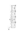
図4は、本開示の1つまたは複数の実施形態による転送データの完全性を与えることに関連したメタデータ形式を示す。図4に示すメタデータ形式は、特定のメモリデバイス(たとえば図2に示すメモリデバイス210)と関連づけられたメタデータ形式である。一例として、図4に示すメタデータ形式をSLC NANDメモリデバイスと関連づけることができる。
FIG. 4 illustrates a metadata format associated with providing transfer data integrity in accordance with one or more embodiments of the present disclosure. The metadata format shown in FIG. 4 is a metadata format associated with a specific memory device (for example, the
図4に示すメタデータ形式は、たとえば図3に示すホストメタデータ形式と対比される調整メタデータ形式である。図4のデータグループ460は、たとえば、図2に関連して先に説明したコントローラ208の完全性コンポーネント224によって形成されうる。データグループ460は複数のデータグループの中の1つであってよく、その各データグループは、たとえば書き込み動作に関連してホストから受信したいくつかのセクターの中の少なくとも1つを、それに対応するメタデータとともに含むものである。本明細書において、このデータグループ460がコードワード460と呼ばれる。
The metadata format shown in FIG. 4 is an adjustment metadata format that is compared with the host metadata format shown in FIG. 3, for example. The
図4に示した例では、コードワード460はペイロード部分445を含み、ペイロード部分445は2つのセクターデータフィールド448−0および448−1を含む。この例において、コードワード460は、2つの512Bセクター(たとえばフィールド448−0に対応するUSER SECTOR0とフィールド448−1に対応するUSER SECTOR1)とともにメタデータ447を含む。図4には示していないが、4KBのデータページは4個のコードワード460(たとえば、第3および第4のユーザーセクターを含む第1の追加コードワード460、第5および第6のユーザーセクターを含む第2の追加コードワード460、第7および第8のユーザーセクターを含む第3の追加コードワード460がそれぞれの対応メタデータ447とともに含まれる)を含むことができ、そのことを読み手が認識する。この例において、メタデータ447には56Bのデータが含まれる。このようにして、各コードワード460には、1KBのペイロード(たとえば2つの512Bセクター)および56Bの利用可能メタデータが含まれる。したがって、メモリデバイスに対する1ページのデータの書き込みには、4320Bのデータ(たとえば4KBのページサイズに対応する4KBのユーザーデータと320Bのメタデータ)の書き込みが含まれうる。
In the example shown in FIG. 4,
コードワード460と関連づけられたメタデータ447は、いくつかのデータフィールドを含む。図4に示す矢印は、特定の完全性データフィールドの対象データ部分を示すために使用される。この例において、フィールド450−0は、フィールド448−0のユーザーセクターと関連づけられた8BのDIFデータ(たとえばSECTOR0 DIF)を含む完全性データフィールドである。すなわち、フィールド450−0には、SECTOR0が完全性コンポーネント224に与えられる前に(たとえば図2に示した挿入コンポーネント220を介して)SECTOR0に付加されるメタデータ(たとえば341)を含めることができる。同様に、フィールド450−1は、フィールド448−1のユーザーセクターと関連づけられた8BのDIFデータ(たとえばSECTOR1 DIF)を含む完全性データフィールドである。すなわち、フィールド450−1には、SECTOR1を完全性コンポーネント224に与える前に(たとえば図2に示した挿入コンポーネント220を介して)SECTOR1に付加されるメタデータ(たとえば341)を含めることができる。
メタデータ447のデータフィールド452は、コードワード460が対応する1ページのデータと関連づけられたアドレスデータを含む4Bのデータ完全性フィールドである。アドレスデータ(図中のFLASH LBA)は、フィールド448−0および448−1のユーザーデータセクターが対応するデータの論理ページと関連づけられた論理ブロックアドレス(LBA)であってよい。同じページに対応する複数の異なるコードワード460のフィールド452を検査して、そのページに対応するいくつかのコードワードについてアドレスデータの完全性が維持されているか判定することができる。
メタデータ447のデータフィールド454−0は、2Bのエラーデータフィールドである。この例において、フィールド454−0に対応するエラーデータ(図中のFLASH CRC SECTOR0)は、フィールド448−0、450−0および452に対応するデータを対象とするCRC(たとえば、SECTOR0対応ページの512BのUSER SECTOR0、8BのSECTOR0 DIF、および4BのFLASH LBAを対象とするCRC)である。同様に、メタデータ447のデータフィールド454−1は、2Bのエラーデータフィールドである。この例において、フィールド454−1に対応するエラーデータ(図中のFLASH CRC SECTOR1)は、フィールド448−1、450−1および452に対応するデータを対象とするCRC(たとえば、SECTOR1の対応ページの512BのUSER SECTOR1、8BのSECTOR1 DIF、および4BのFLASH LBAを対象とするCRC)である。図4に示す調整メタデータ形式のデータフィールド452、454−0、および454−1には、図2に関連して先に説明したように第2の完全性データと呼ばれるデータを含めることができる。
A data field 454-0 of the
この例において、メタデータ447のデータフィールド456は4Bの予備データフィールドである。メモリシステム(たとえば図1に示すメモリシステム104)内部のデータ転送に関連して、フィールド456をさまざまな目的に使用することができる。たとえば、フィールド456には、ペイロード445に関する追加エラーデータおよび/またはその他の完全性データを含めることができる。しかし、フィールド456をデータ完全性以外の目的に使用することもできる。
In this example, the
メタデータ447のデータフィールド458は、28Bのエラーデータフィールドである。この例において、フィールド458(図中のBCHECC16)に対応するエラーデータは、ペイロード445(たとえばUSER SECTOR0およびUSER SECTOR1)に対応する1024Bのユーザーデータおよびそれと関連づけられた56Bのメタデータ447を対象とする16ビットのエラー訂正コード(ECC)である。このようにして、フィールド458に対応するエラーデータは、各コードワード460(たとえば1080Bごと)の16ビット訂正をサポートする。実施形態は、この例に限定されない。図4に示す調整メタデータ形式のデータフィールド458は、図2に関連して先に説明したように第3の完全性データと呼ばれうる。
A
図4に示す調整メタデータ形式は、コントローラを介して実装され、図2に関連して先に説明したようにホストからの書き込みおよび読み出し要求などの動作に関連してデータ完全性を与える目的で使用されうる。たとえば、完全性コンポーネント224は、ホストからの受信セクターと関連づけられたメタデータ形式を第1の形式(たとえば図3に示したようなホスト形式)から第2の形式(たとえば図4に示したような調整形式)に変換することができる。メモリデバイス210に書き込まれるコードワード(たとえば460)には、コンポーネント226によって生成されたエラーデータが含まれるエラーデータフィールド(たとえば458)が含まれうる。このエラーデータは、当該コードワードの他のメタデータ(たとえばフィールド458以外のデータフィールドに対応するメタデータ447のデータ)およびペイロード(たとえば445)を対象とする。他のメタデータおよびペイロードに関するエラーデータは、当該コードワードが(たとえばホストからの読み出し要求に応答して)メモリデバイス210から読み出される時点で、コンポーネント230を介して検査することができる。読み出し要求が部分ページ読み出し要求であるかフルページ読み出し要求であるかにかかわらず、コントローラ208は、要求セクターをホストに配信する前に、デバイスから読み出されたコードワードに関連づけられたメタデータ形式を変換して調整メタデータ形式からホスト形式に戻すように構成されており、その過程でデータセクターのデータ完全性が維持されている。
The coordination metadata format shown in FIG. 4 is implemented via a controller and is intended to provide data integrity in connection with operations such as write and read requests from the host as described above in connection with FIG. Can be used. For example, the
図5は、本開示の1つまたは複数の実施形態による転送データの完全性を与えることに関連したメタデータ形式を示す。図5に示すメタデータ形式は、特定のメモリデバイス(たとえば図2に示すメモリデバイス210)と関連づけられたメタデータ形式である。一例として、図5に示すメタデータ形式をMLC NANDメモリデバイスと関連づけることができる。
FIG. 5 illustrates a metadata format associated with providing transfer data integrity in accordance with one or more embodiments of the present disclosure. The metadata format shown in FIG. 5 is a metadata format associated with a specific memory device (for example, the
図5に示すメタデータ形式は、たとえば図3に示したホストメタデータ形式と対比される調整メタデータ形式である。図5に示す第1のデータグループ560−0および第2のデータグループ560−1は、たとえば図2に関連して先に説明したコントローラ208の完全性コンポーネント224およびコンポーネント226によって形成されうる。データグループ560−0および560−1は、コードワード560−0および560−1と呼ばれうる。
The metadata format shown in FIG. 5 is an adjustment metadata format that is compared with the host metadata format shown in FIG. 3, for example. The first data group 560-0 and the second data group 560-1 shown in FIG. 5 may be formed, for example, by the
図5に示した例では、コードワード560−0および560−1は、それぞれのペイロード部分545−0および545−1とともに、それぞれのメタデータ547−0および547−1を含む。この例において、コードワード560−0と560−1の各々は、2つのセクターデータフィールドを含む(たとえばコードワード560−0はセクターフィールド548−0および548−1を含み、コードワード560−1はセクターフィールド548−2および548−3を含む)。コードワード560−0は、2つの512Bセクター(たとえばフィールド548−0に対応するUSER SECTOR0とフィールド548−1に対応するUSER SECTOR1)を含む。コードワード560−1は、2つの512Bセクター(たとえばフィールド548−2に対応するUSER SECTOR2およびフィールド548−3に対応するUSER SECTOR3)を含む。図5には示していないが、4KBのデータページは4個のコードワード(たとえば、第5および第6のユーザーセクターを含む追加コードワード560−0、第7および第8のユーザーセクターを含む追加コードワード560−1がそれぞれの対応メタデータ547−0および547−1とともに含まれる)を含むことができ、そのことを読み手が認識する。この例において、メタデータ547−0/547−1には、56Bのデータが含まれる。このようにして、各コードワードには、1024Bのペイロード(たとえば2つの512Bセクター)および56Bの利用可能メタデータが含まれる。したがって、メモリデバイスに対する1ページのデータの書き込みには、4320Bのデータ(たとえば4KBのページサイズに対応する4KBのユーザーデータと320Bのメタデータ)の書き込みが含まれうる。 In the example shown in FIG. 5, codewords 560-0 and 560-1 include respective metadata 547-0 and 547-1 along with respective payload portions 545-0 and 545-1. In this example, each of codewords 560-0 and 560-1 includes two sector data fields (eg, codeword 560-0 includes sector fields 548-0 and 548-1, and codeword 560-1 is Including sector fields 548-2 and 548-3). Codeword 560-0 includes two 512B sectors (eg, USER SECTOR0 corresponding to field 548-0 and USER SECTOR1 corresponding to field 548-1). Codeword 560-1 includes two 512B sectors (eg, USER SECTOR2 corresponding to field 548-2 and USER SECTOR3 corresponding to field 548-3). Although not shown in FIG. 5, a 4 KB data page includes four codewords (eg, an additional codeword 560-0 including fifth and sixth user sectors, an additional including seventh and eighth user sectors). Codeword 560-1 may be included with each corresponding metadata 547-0 and 547-1), which is recognized by the reader. In this example, the metadata 547-0 / 547-1 includes 56B data. Thus, each codeword includes 1024B of payload (eg, two 512B sectors) and 56B of available metadata. Thus, writing one page of data to the memory device can include writing 4320 B of data (eg, 4 KB of user data and 320 B of metadata corresponding to a 4 KB page size).
コードワード560−0と関連づけられたメタデータ547−0およびコードワード560−1と関連づけられたメタデータ547−1は、それぞれいくつかのデータフィールドを含む。図5に例示した調整メタデータ形式では、コードワード560−0のメタデータ547−0と関連づけられたデータフィールドがコードワード560−1のメタデータ547−1と関連づけられたデータフィールドと異なる(たとえば56Bの利用可能メタデータが異なる目的で使用される)。図4と同様、図5に示す矢印は、特定の完全性データフィールドの対象データ部分を示すために使用される。 Metadata 547-0 associated with codeword 560-0 and metadata 547-1 associated with codeword 560-1 each include several data fields. In the adjusted metadata format illustrated in FIG. 5, the data field associated with the code word 560-0 metadata 547-0 is different from the data field associated with the code word 560-1 metadata 547-1 (eg, 56B available metadata is used for different purposes). Similar to FIG. 4, the arrows shown in FIG. 5 are used to indicate the subject data portion of a particular integrity data field.
メタデータ547−0のデータフィールド552は、4Bのデータ完全性フィールドであり、コードワード560−0および560−1が対応する1ページのデータと関連づけられたアドレスデータが含まれる。そのアドレスデータ(図中のFLASH LBA)は、フィールド548−0、548−1、548−2、および548−3のユーザーデータセクターが対応するデータの論理ページと関連づけられた論理ブロックアドレス(LBA)であってよい。同じページに対応する別個のコードワード560−0のフィールド552を検査して、そのページに対応するいくつかのコードワードについてアドレスデータの完全性が維持されているか判定することができる。
メタデータ547−1のデータフィールド554は、4Bのエラーデータフィールドである。この例において、フィールド554に対応するエラーデータ(図中のFLASH CRC)は、フィールド548−0、548−1、548−2、548−3、および552に対応するデータを対象とするCRC(たとえば32ビットCRC)である(たとえば512BのUSER SECTOR0、USER SECTOR1、USER SECTOR2、USER SECTOR3および各ユーザーセクターが対応するページの4BのFLASH LBAを対象とするCRC)。図5に示す調整メタデータ形式のデータフィールド552および554には、図2に関連して先に説明したように第2の完全性データと呼ばれるデータを含めることができる。この例において、コードワード560−1と関連づけられたメタデータ547−1は、コードワード560−1と関連づけられたセクター(たとえばUSER SECTOR2およびUSER SECTOR3)とともにコードワード560−0と関連づけられたセクター(たとえばUSER SECTOR0およびUSER SECTOR1)に対応する第2の完全性データ(たとえばデータ完全性フィールド554に対応するCRCの形のエラーデータ)を含む。コードワード560−0と関連づけられたメタデータ547−0も同じく、異なるコードワードと関連づけられたセクターに対応する第2の完全性データ(たとえばデータ完全性フィールド552に対応するアドレスデータ)を含む。すなわち、メタデータ547−0の第2の完全性データ552は、コードワード560−0内のセクターおよび異なるコードワード(たとえば560−1)内のセクターに対応する。このようにして、コードワード560−0/560−1と関連づけられた調整メタデータ形式には、複数のセクター(たとえばこの例におけるセクター0〜3)に対応する第2の完全性データ(たとえばフィールド552および554に対応する完全性データ)が含まれる。
The
メタデータ547−1のメタデータ547−0および558−1のデータフィールド558−0は、それぞれ52Bのエラーデータフィールドである。この例において、フィールド558−0および558−1に対応するエラーデータ(図中のBCHECC29)は29ビットのエラー訂正コード(ECC)であり、それぞれ、ペイロード545−0(たとえばUSER SECTOR0およびUSER SECTOR1)およびペイロード545−1(たとえばUSER SECTOR2およびUSER SECTOR3)に対応する1024Bのユーザーデータとともに、各ユーザーデータと関連づけられた56Bのメタデータ547−0および547−1を対象とする。このようにして、フィールド558−0および558−1に対応するエラーデータは、コードワードごと(たとえば1080Bごと)の29ビット訂正をサポートする。実施形態は、この例に限定されない。図5に示す調整メタデータ形式のデータフィールド558−0および558−1は、図2に関連して先に説明したように第3の完全性データと呼ばれうる。 The metadata 547-0 of the metadata 547-1 and the data field 558-0 of 558-1 are respectively 52B error data fields. In this example, the error data (BCHECC 29 in the figure) corresponding to the fields 558-0 and 558-1 is a 29-bit error correction code (ECC) and has a payload 545-0 (for example, USER SECTOR0 and USER SECTOR1), respectively. And 56B metadata 547-0 and 547-1 associated with each user data, as well as 1024B user data corresponding to payload 545-1 (eg, USER SECTOR2 and USER SECTOR3). In this way, the error data corresponding to fields 558-0 and 558-1 supports 29 bit correction per codeword (eg every 1080B). The embodiment is not limited to this example. The adjustment metadata format data fields 558-0 and 558-1 shown in FIG. 5 may be referred to as third integrity data as described above in connection with FIG.
コードワード560−0および560−1を当該データのページに対応する追加コードワードとともにメモリデバイス(たとえばメモリデバイス210)に書き込むことができる。たとえば、読み出し動作に応答して、メタデータ547−0および547−1の第3の完全性データ(たとえば完全性データフィールド558−0および558−1のECCコード)を検査することができる。第3の完全性データの検査は、図2に示すコンポーネント230などのコンポーネントによって実行することができる。いくつかの実施形態において、第3の完全性データの検査実行後、メタデータ547−0および547−1の第2の完全性データ(たとえばデータ完全性フィールド554のCRC)の検査を(たとえば完全性コンポーネント234によって)実行することができる。いくつかの実施形態において、完全性コンポーネント234は、1セクター単位で、いくつかのコードワードの中の特定の1つのコードワード内の少なくとも1つのセクター(たとえばコードワード560−0のUSER SECTOR0)に対応する第4の完全性データを生成することができる。上述のように、コンポーネント234は、いくつかのコードワードの中の特定の1つと関連づけられたメタデータ(たとえばコードワード560−0と関連づけられたメタデータ547−0)を少なくとも1つのセクター(たとえばUSER SECTOR0)に対応する調整メタデータ(たとえば図3に示すメタデータ341などのホスト形式を有するメタデータ)に置き換えることができる。この調整メタデータには、第4の完全性データ(たとえばUSER SECTOR0に対応するCRCなどのエラーデータ)が含まれる。
Codewords 560-0 and 560-1 can be written to a memory device (eg, memory device 210) along with an additional codeword corresponding to the page of data. For example, in response to a read operation, the third integrity data of metadata 547-0 and 547-1 (eg, the ECC code of integrity data fields 558-0 and 558-1) can be examined. The third integrity data check may be performed by a component, such as
いくつかの実施形態において、コンポーネント236などのコンポーネントは、いくつかのコードワードの中の特定の1つのコードワード内の少なくとも1つのセクターに対応する調整(たとえば修正)メタデータの第4の完全性データの検査を実行することができる。第4の完全性データの検査には、いくつかのコードワードの中の特定の1つのコードワード内の少なくとも1つのセクターに対応する修正メタデータの第4の完全性データとその少なくとも1つのセクターに対応する第1の完全性データとの比較を含めることができる。たとえば、コンポーネント236は、第4の完全性データ(たとえば完全性コンポーネント234によって生成されたCRC)を以前に生成されたCRC(たとえば挿入コンポーネント220によって生成され、コントローラのバッファに格納されたもの)と比較することができる。いくつかの実施形態において、その少なくとも1つのセクターをホストに転送する前に、その少なくとも1つのセクターに対応する調整メタデータを(たとえばコンポーネント236を介して)削除することができる。しかし、先に示したように、いくつかの実施形態において、コンポーネント236が(たとえばコンポーネント234から)受け取った修正メタデータの1つまたは複数の部分を削除しないままホストインタフェース206に与えることができる。
In some embodiments, a component, such as
たとえば、部分読み出し動作に応答して、メタデータ547−0および547−1の第3の完全性データ(たとえば完全性データフィールド558−0および558−1のECCコード)を検査することもできる。そのような実施形態において、第3の完全性データの検査は、図2に示すコンポーネント230などのコンポーネントによって実行することができる。いくつかの実施形態において、第3の完全性データの検査実行後、メタデータ547−0および547−1の第2の完全性データ(たとえばデータ完全性フィールド554のCRC)の検査を(たとえば結合コンポーネント228によって)実行することができる。結合コンポーネント228は、メタデータ547−0および547−1の第2の完全性データの検査後、メタデータを図5に示す調整形式からホスト形式(たとえば図3に示すようなセクターごとに完全性データを含む形式)に変換するように構成される。結合コンポーネント228は、メモリデバイス210から読み出されたページの1つまたは複数のセクターを部分読み出し動作に関連して受け取った1つまたは複数のホストセクターに置き換えることができ、また、そのデータおよび関連メタデータを完全性コンポーネント224に転送することができる。完全性コンポーネント224は、上述のようなホスト形式によるデータを受け取るように構成される。いくつかの部分読み出し動作において、結合コンポーネント228は、メモリデバイス210から読み出されたページに対応する各コードワード(たとえばコードワード560−0、560−1および読み出しページに対応するその他のコードワード)の第2の完全性データの検査を実行しなくてもよい。たとえば、メモリデバイスから読み出されて6個のホストセクターと結合される2個のセクター(たとえばUSER SECTOR0とUSER SECTOR1)が部分読み出しに含まれる場合、結合コンポーネント228は、完全性データフィールド554の完全性データ(たとえばフィールド548−1、548−2、548−3、548−4、および552に対応するCRC)を検査することができる。しかし、その読み出しページに対応する他のコードワードにはホストセクターと結合されるセクターが含まれないため、それらのコードワードに関連づけられた第2の完全性データの検査を実行しないように結合コンポーネント228を構成することができる。同様に、この部分読み出しの例に関連して、ホストセクターと結合されるセクターを含まない読み出しページ内のコードワードと関連づけられたメタデータについて、調整形式からホスト形式への変換を実行しないように結合コンポーネント228を構成することができる。部分読み出し動作と関連づけられたセクターを含まないコードワードのメタデータを変換しないこと、かつ/またはそのメタデータと関連づけられた第2の完全性データを検査しないことにより、処理リソースを節約できるほか、さまざまな利益がもたらされる。
For example, in response to a partial read operation, third integrity data of metadata 547-0 and 547-1 (eg, ECC codes of integrity data fields 558-0 and 558-1) may be examined. In such an embodiment, the third integrity data check may be performed by a component, such as
図6は、本開示の1つまたは複数の実施形態によるメモリコントローラ608の機能ブロック図である。コントローラ608は、図1に関連して説明したコントローラ108などのコントローラまたは図2に関連して説明したコントローラ208などのコントローラであってよい。
FIG. 6 is a functional block diagram of a
図6に示す例において、コントローラ608は、メモリ管理コンポーネント613およびメモリ制御コンポーネント611を備える。メモリ管理コンポーネント613は、ウエアレベリング(たとえばガーベジコレクションおよび/または再使用)、エラー検出および/または訂正、ブロック除外など、メモリデバイス610−1〜610−Nに関する各種のメモリ管理機能と関連づけられたコンポーネント(たとえば回路および/またはファームウェア)を含む。メモリ管理コンポーネント613は、ホストコマンド(たとえば、ホストインタフェース606を介してホストから受信するコマンド)を解析および/またはフォーマットして、複数のデバイスコマンド(たとえばメモリデバイス610−1〜610−Nの操作に関連したコマンド)に変換することができる。メモリ管理コンポーネント613は、(たとえば各種のメモリ管理機能を達成する目的で)デバイスコマンドを生成することもできる。メモリ管理コンポーネント613は、メモリ制御コンポーネント611にデバイスコマンドを与えるように構成される。
In the example illustrated in FIG. 6, the
メモリ制御コンポーネント611は、いくつかのメモリデバイス610−1〜610−Nに対するデータの書き込み、メモリデバイス610−1〜610−Nからのデータの読み出し、およびメモリデバイス610−1〜610−N内のデータ(たとえば複数のブロック)の消去に関連したメモリ動作を制御するように構成される。それらのメモリ動作は、ホストコマンド(たとえばホストインタフェース606を介してコントローラ608に送られたホストコマンド)に基づく動作(たとえば読み出しおよび/または書き込み)であってよく、ならびに/または(たとえばウエアレベリング、エラー検出および/または訂正などに関連して)制御コンポーネント611および/もしくはメモリ管理コンポーネント613によって開始される内部的に生成されたデバイスコマンドに基づくものであってよい。
The
制御コンポーネント611に結合されたメモリデバイス610−1〜610−Nは、図1で説明したデバイス110−1〜110−Nなどの不揮発性メモリデバイスであってよい。図6に示す例において、メモリデバイス610−1〜610−Nは、NANDフラッシュメモリデバイスである。上述のように、メモリデバイス610−1〜610−N内のメモリセルをいくつかの物理ページと関連づけ、それらの物理ページを有するいくつかのブロックに編成することができる。
Memory devices 610-1 to 610-N coupled to control
メモリ制御コンポーネント611はエラー訂正コンポーネント619を含み、そのエラー訂正コンポーネント619には、メモリデバイス610−1〜610−Nに対する書き込みおよび/もしくは読み出しが行われるデータに関連するエラーを検出ならびに/または訂正するように構成されたECCエンジンあるいはその他の回路を含むことができる。いくつかの実施形態において、エラー訂正コンポーネント619は、提供されたデータ内のビットエラーを検出するためにBCHECC(たとえば図2、図4および図5に関連して先に説明した機能など)を利用することができる。検出されたビットエラーには、エラー訂正コンポーネント619によって訂正可能な場合と訂正不可能な場合がある(たとえば検出された誤りビットの数および使用ECCの種類などに依存する)。いくつかの誤りビットがコンポーネント619によって訂正可能である場合、当該動作は訂正可能ビットエラーであり、コンポーネント619は、その特定動作の完了に伴ってエラー訂正の処理に進むことができる。いくつかの誤りビットがコンポーネント619によって訂正可能でない(たとえば誤りビットの数がコンポーネント619に関連する訂正可能ビット数の閾値を超える)場合、当該動作は訂正不可能ビットエラーである。訂正可能ビットエラーおよび訂正不可能ビットエラーをメモリ管理コンポーネント613に報告するようにメモリ制御コンポーネント611を構成することができる。
The
メモリ管理コンポーネント613は、いくつかの管理テーブル615を備える。テーブル615には、メモリデバイス610−1〜610−Nに関連した各種の情報を保持することができる。たとえば、デバイス610−1〜610−N内のブロックに関するブロックエイジおよび/またはブロック消去回数に関する情報をテーブル615に含めることができる。また、メモリデバイス610−1〜610−Nと関連づけられたブロックおよび/またはページに関連するエラー履歴に関する情報をテーブル615に含めることができる。たとえば、テーブル615は、デバイス610−1〜610−Nに関連したいくつかのエラー数(たとえば書き込み動作エラー数、読み出しビットエラー数、読み出し動作エラー数および/または消去エラー数を含む各種エラー数)を保持することができる。書き込み動作エラーは、実行が失敗した書き込み動作(たとえばホスト開始またはデバイス開始による動作)を指す。読み出し動作エラーは、実行が失敗した読み出し動作(たとえばホスト開始またはデバイス開始による動作)を指す。読み出しビットエラーは、結果的にデータ(たとえばページ)の読み出しに関連したいくつかのエラービットが検出される読み出し動作を指すことができる。上述のように、いくつかの検出エラーには、エラー訂正コンポーネント(たとえば619)によって訂正可能な場合と訂正不可能な場合がある。検出エラーの数がエラー訂正コンポーネント(たとえば619)によって訂正可能なエラー数の閾値を超える場合、そのビットエラーは訂正不可能ビットエラーと呼ばれる。テーブル615は、メモリデバイス610−1〜610−Nと関連づけられたブロックに発生した訂正可能および/または訂正不可能な読み出しビットエラーの数を保持することができる。テーブル615には、LBAテーブルなどの各種テーブルを含めることもできる。
The
コントローラ608のメモリ管理コンポーネント613は、冗長管理コンポーネント617を含む。この冗長管理コンポーネント617はRAID(独立ディスク冗長アレイであって、ここでの用語「ディスク」はハードディスクドライブを使用した従来の実装を単純に引き継いだもの)ユニット617であってよい。RAIDユニット617を使用することにより、RAIDとしてのメモリデバイスの運用に伴う冗長性を通じて、データ信頼性が提供されうる。RAIDユニット617は、たとえばRAID排他的論理和(XOR)回路など、さまざまなRAIDレベルと関連づけられた各種回路を含むことができる。
The
いくつかの実施形態において、コントローラ608は、ホストインタフェース606とメモリデバイス610−1〜610−Nとの間で転送されるデータの完全性を維持しながら、読み出しおよび書き込み動作など、各種の動作に関連したエラー発生(たとえばビットエラーおよび/または動作エラー)の動的な検出および回復を行うように構成される。コントローラ608は、将来の訂正不可能エラーを防止するために障害メモリリソース(たとえばページ、ブロック、および/またはデバイス610−1〜610−N)を利用から除外するように構成される。
In some embodiments, the
たとえば、メモリ管理コンポーネント613は、メモリ制御コンポーネント611に対して(たとえばメモリデバイス610−1〜610−N内のブロックの書き込み準備のために)消去コマンドの実行を開始することができる。制御コンポーネント611は、消去動作に関連した消去エラーの発生を検出するとともに、そのエラー発生をメモリ管理コンポーネント613に報告することができる。消去エラーの場合、当該ブロック内の有効データはすべて消去動作の実行前に別のブロックに移動されているため、データ回復の必要はない。消去エラーに関連したブロックは、消去エラー数が閾値に達した時点で除外することができる。いくつかの実施形態において、消去エラー数の閾値は1であるが、実施形態はこれに限定されない。
For example, the
さまざまな実施形態において、コントローラ608は、各種のデバイス動作および/またはホスト動作(たとえば読み出しおよび/または書き込み動作など)を実行する一方で、ウエアレベリング機能(たとえばガーベジコレクションおよび/または再使用)、エラー検出/訂正機能(たとえばECC関連)、ページおよび/またはブロック除外機能、RAID機能など、メモリデバイス610−1〜610−Nに関連した各種のメモリ管理機能を実行することができる。このようにして、ユーザーに知覚される影響なしに、各種のメモリ管理機能を実行することができる。本明細書に説明する実施形態に従ってデータ完全性を維持しながらエラー回復動作を実行できるコントローラ608の機能により、実施されるデバイス製造試験(たとえば消費者に引き渡す前の現場の出荷前試験)の量を減少させることができる。たとえば、本開示の実施形態は、不良ブロックまたは不良メモリデバイス(たとえば610−1〜610−N)の位置の判定に関連したデバイス製造試験の発生を低減または防止することができる。図6に示すコンポーネント(たとえば611、613、615、617、および619)などのハードウェアコンポーネントによって、そのような試験を現場で実施できるためである。すなわち、メモリデバイス610−1〜610−Nは、メモリデバイス610−1〜610−Nに関連付けられた不良ブロック位置に関して無試験とすることができる。当該試験をコントローラ608のハードウェアコンポーネントに移すことによるメモリデバイス(たとえば610−1〜610−N)の出荷前試験の減少および/または廃止によって、デバイスの出荷前試験に関連したコスト低減が可能になる一方、ユーザーに知覚される影響が生じることは、あったとしてもごくわずかである。
In various embodiments, the
一例として、ホスト読み出し動作に関連して、メモリデバイス610−1〜610−Nから読み出されたデータをエラー訂正コンポーネント619によって検査し、データ内のビットエラーを判定(たとえば検出)することができる。いくつかのビットエラー(たとえば存在する場合)が検出され、そのビットエラー数がコンポーネント619によって訂正可能なビットエラー数の閾値より少ない(たとえば当該ビットエラーが訂正可能ビットエラーである)場合には、データが訂正されてホストに提供される。訂正可能ビットエラーの発生はメモリ管理コンポーネント613に報告される。メモリ管理コンポーネント613は、データが読み出されたブロックに関連するビットエラー数(たとえば訂正可能ビットエラーの数)を(たとえばテーブル615に)保持することができ、ビットエラー数が特定のビットエラー数閾値を超えた場合、そのブロックを除外することができる。検出ビットエラーの数がコンポーネント619によって訂正可能なビットエラー数の閾値を上回る(たとえば当該ビットエラーが訂正不可能ビットエラーである)場合には、要求された読み出しデータをRAIDユニット617によって自動的に回復させてからホストに提供することができる。いくつかの実施形態において、メモリ管理コンポーネント613は、受信される訂正不可能ビットエラーの発生指示(たとえばエラー訂正コンポーネント619からの報告による)に応答して、自動的に読み出しデータの回復を開始する。メモリ管理コンポーネント613は、データが読み出されたブロックに関連するビットエラー数(たとえば訂正不可能ビットエラーの数)を(たとえばテーブル615に)保持することができ、ビットエラー数が特定のビットエラー数閾値を超えた場合には、そのブロックを除外することができる。(たとえばビットエラー数の閾値を超えるビットエラー数に応答して)ブロックを除外する前に、RAIDユニット617を使用して、そのブロックに関連したデータを回復させることができ、さらにそのデータを新しいブロック(たとえば利用可能な有効ブロック)に移動させることができる。
As an example, in connection with a host read operation, data read from memory devices 610-1 through 610-N can be examined by
デバイス読み出し動作(たとえば再使用などのメモリ管理プロセスに関連して制御コンポーネント611によって開始された読み出し動作)に関連するビットエラーは、同様に扱うことができる。たとえば、訂正可能ビットエラーがコンポーネント619によって検出された場合、当該データを訂正し、メモリデバイス610−1〜610−N内の新しいブロックに移動させることができる(対照的にホスト読み出し動作の場合はデータがホストに渡される)。訂正可能ビットエラーの発生はメモリ管理コンポーネント613に報告され、メモリ管理コンポーネント613は、データが読み出されたブロックに関連するビットエラー数を保持することができ、ビットエラー数が特定のビットエラー数閾値を超えた場合には、そのブロックを除外することができる。検出ビットエラーの数がコンポーネント619によって訂正可能なビットエラー数の閾値を上回る(たとえば当該ビットエラーが訂正不可能ビットエラーである)場合、RAIDユニット617を使用して、要求された読み出しデータをただちに回復させることができ、さらにそのデータを新しいブロックに移動させることができる。訂正不可能ビットエラーの発生はメモリ管理コンポーネント613に報告され、メモリ管理コンポーネント613は、データが読み出されたブロックに関連するビットエラー数を保持することができ、ビットエラー数が特定のビットエラー数閾値を超えた場合には、そのブロックを除外することができる。(たとえばビットエラー数の閾値を超えるビットエラー数に応答して)ブロックを除外する前に、そのブロックに関連したデータをRAIDユニット617によって回復させることができ、そのデータを新しいブロック(たとえば利用可能な有効ブロック)に移動させることができる。
Bit errors associated with device read operations (eg, read operations initiated by
読み出し動作エラー(たとえばホスト読み出し動作エラーおよびデバイス読み出し動作エラー)は、ホストおよびデバイス読み出し動作に対応するビットエラーに関連して先に説明した方法と同様に扱うことができる。たとえば、読み出し要求が失敗した場合、その失敗の指示をメモリ管理コンポーネント613に与えることができ、メモリ管理コンポーネント613は、要求された読み出しデータの回復を(たとえばRAIDユニット617によって)自動的に開始することができる。
Read operation errors (eg, host read operation errors and device read operation errors) can be handled in a manner similar to that described above in connection with bit errors corresponding to host and device read operations. For example, if a read request fails, an indication of the failure can be provided to the
書き込み動作エラー(たとえばホスト書き込み動作エラーおよびデバイス書き込み動作エラー)は、ホストおよびデバイス読み出し動作に対応するビットエラーおよび/または読み出し動作エラーに関連して先に説明した方法と同様に扱うことができる。たとえば、書き込み要求が失敗した場合、その失敗の指示をメモリ管理コンポーネント613に与えることができ、メモリ管理コンポーネント613は、要求された書き込みデータの回復を(たとえばRAIDユニット617によって)自動的に開始することができる。いくつかの実施形態において、メモリ管理コンポーネント613は、受信される書き込みエラーの発生指示(たとえば制御コンポーネント611からの報告による)に応答して、自動的に書き込みデータの回復を開始する。メモリ管理コンポーネント613は、データが書き込まれたブロックに関連する書き込みエラー数を(たとえばテーブル615に)保持することができ、書き込みエラー数が特定の書き込みエラー数閾値を超えた場合には、そのブロックを除外することができる。書き込みデータの自動回復(たとえばRAIDユニット617による)に関して、回復された書き込みデータは新しいブロック(たとえば利用可能な有効ブロック)に移動させることができる。
Write operation errors (eg, host write operation errors and device write operation errors) can be handled in a manner similar to that described above in connection with bit errors and / or read operation errors corresponding to host and device read operations. For example, if a write request fails, an indication of the failure can be provided to the
<結論>
本開示は、データ完全性を与えるための装置(たとえばコンピューティングシステム、メモリシステム、コントローラなど)および方法を含む。1つまたは複数の方法実施形態には、たとえば、いくつかのメモリデバイス(たとえば単一メモリデバイス)に書き込まれるデータのいくつかのセクターを受け取ること、およびそのいくつかのセクターに対応する第1のメタデータを付加するとともに、そのいくつかのセクターに第1の完全性データを含めることが含まれ、この第1のメタデータは特定の形式を有するものである。方法実施形態にはさらに、第2のメタデータで与えられる第2の完全性データを生成することが含まれ、この第2の完全性データはいくつかのセクターの中の少なくとも1つに対応するものである(第2のメタデータは第2の形式を有する)。方法実施形態にはさらに、第2のメタデータで与えられる第3の完全性データを生成することが含まれ、この第3の完全性データは、第2の完全性データおよびいくつかのセクターの中の少なくとも1つに対応するエラーデータを含むものである。
<Conclusion>
The present disclosure includes devices (eg, computing systems, memory systems, controllers, etc.) and methods for providing data integrity. One or more method embodiments include, for example, receiving a number of sectors of data to be written to a number of memory devices (eg, a single memory device) and a first corresponding to the number of sectors. It includes adding metadata and including first integrity data in some of its sectors, the first metadata having a specific format. The method embodiment further includes generating second integrity data provided in the second metadata, the second integrity data corresponding to at least one of the several sectors. (The second metadata has the second format). The method embodiment further includes generating third integrity data provided in the second metadata, wherein the third integrity data includes the second integrity data and the number of sectors. Error data corresponding to at least one of them is included.
当然ながら、1つの要素が別の要素「上」、別の要素「に接続」、または別の要素「と結合」と記載されている場合、その「上」、「接続」、または「結合」は直接的な関係でありうるか、介在要素が存在することもありうる。一方、1つの要素が別の要素の「直上」、別の要素に「直接的に接続」または別の要素と「直接的に結合」と記載されている場合には、介在要素または階層は存在しない。本明細書における用語の「および/または」は、列挙された1つまたは複数の関連項目のあらゆる組み合わせを含む。 Of course, when one element is described as “on” another element, “connected to” another element, or “coupled with” another element, “on”, “connected”, or “coupled” Can be a direct relationship or there can be intervening elements. On the other hand, if one element is described as “directly above” another element, “directly connected” to another element, or “directly coupled” with another element, there is an intervening element or hierarchy do not do. As used herein, the term “and / or” includes any combination of one or more of the associated listed items.
本明細書において使用される用語の「および/または」は、列挙された1つまたは複数の関連項目のあらゆる組み合わせを含む。本明細書において使用される用語の「または」は、特段の注記がないかぎり、包含的論理和を意味する。すなわち、「AまたはB」には、(Aのみ)、(Bのみ)、または(AとBの両方)が含まれうる。言い換えれば、「AまたはB」は、「Aおよび/またはB」あるいは「AとBの一方または両方」という意味である。 As used herein, the term “and / or” includes any combination of one or more of the associated listed items. As used herein, the term “or” means inclusive OR, unless otherwise noted. That is, “A or B” may include (A only), (B only), or (both A and B). In other words, “A or B” means “A and / or B” or “one or both of A and B”.
当然ながら、本明細書では各種の要素を記述するために第1、第2、第3などの用語を使用することがあるが、それらの要素は、これらの用語によって限定されるべきではない。これらの用語は、1つの要素を別の要素と区別するためにのみ使用されている。したがって、本開示の教示内容から逸脱することなく、第1の要素が第2の要素と呼ばれることもありえる。 Of course, terms such as first, second, third, etc. may be used herein to describe various elements, but these elements should not be limited by these terms. These terms are only used to distinguish one element from another. Accordingly, the first element may be referred to as the second element without departing from the teachings of the present disclosure.
本明細書には具体的な実施形態が例示および説明されているが、当業者によって理解されるように、本明細書中の具体的な実施形態の代替として、同じ結果を達成するように考案された仕組みを用いることができる。本開示は、本開示の1つまたは複数の実施形態の改作物または変形を包含することを意図している。当然ながら、上述の説明は例示的な方法で行われており、制限的ではない。上述の説明を精査することにより、当業者には上述の実施形態と、本明細書に具体的に説明されていない他の実施形態との組み合わせが明らかになるはずである。本開示の1つ以上または複数の実施形態の範囲には、上述の構造および方法を使用する他の用途が含まれる。したがって、本開示の1つ以上または複数の実施形態の範囲は、添付の請求項を参照するとともに、それらの請求項に対して認められる均等物の全範囲を考慮して確定されるべきである。 Although specific embodiments are illustrated and described herein, as will be appreciated by those skilled in the art, they are devised to achieve the same results as alternatives to the specific embodiments herein. Can be used. This disclosure is intended to cover adaptations or variations of one or more embodiments of the present disclosure. Of course, the above description is provided by way of example and not limitation. Upon review of the above description, those skilled in the art will appreciate combinations of the above embodiments with other embodiments not specifically described herein. The scope of one or more embodiments of the present disclosure includes other applications using the structures and methods described above. Accordingly, the scope of one or more embodiments of the disclosure should be determined with reference to the appended claims, along with the full scope of equivalents to which such claims are entitled. .
上述の「発明を実施するための形態」においては、開示内容を簡潔にする目的で、いくつかの特徴が1つの実施形態にまとめられている。この開示方法は、本明細書に開示された実施形態が各請求項に明示的に記載されているよりも多くの特徴を必要とするという意図を反映したものと解釈されるべきではない。正しくは、以下の請求項に反映されているように、発明的主題は1つの開示された実施形態のすべての特徴よりも少ない中に存在する。したがって、本明細書により、以下の請求項は「発明を実施するための形態」に組み込まれるものとし、各請求項は別個の実施形態として自立している。 In the above-mentioned “Mode for Carrying Out the Invention”, for the purpose of simplifying the disclosure, several features are combined into one embodiment. This method of disclosure is not to be interpreted as reflecting an intention that the embodiments disclosed herein require more features than are expressly recited in each claim. Rather, as reflected in the following claims, the inventive subject matter lies in less than all the features of one disclosed embodiment. Accordingly, the following claims are hereby incorporated into the Detailed Description, with each claim standing on its own as a separate embodiment.
Claims (20)
前記いくつかのメモリデバイスに関するいくつかのメモリ動作に関連したエラー発生を判定することと、
前記いくつかのメモリ動作の中の特定の1つに関連したエラー発生の指示に応答して、前記いくつかのメモリ動作の中の特定の1つに関するデータの回復を自動的に開始することと
を目的に構成される、前記装置。 An apparatus comprising a controller configured to be coupled to a number of memory devices, the controller comprising:
Determining an occurrence of an error associated with some memory operation for the some memory device;
Automatically initiating data recovery for a particular one of the number of memory operations in response to an indication of an error associated with a particular one of the number of memory operations; The apparatus configured for the purpose.
前記いくつかの異なるメモリ動作の中の特定の1つと関連づけられたブロックに関連したエラー発生の回数を判定することと、
閾値エラー数を超える前記ブロックに関連した前記エラー発生の回数に応答して、前記ブロックを除外することと
を目的に構成される、請求項4の装置。 The controller is
Determining the number of error occurrences associated with a block associated with a particular one of the several different memory operations;
5. The apparatus of claim 4, wherein the apparatus is configured to exclude the block in response to the number of occurrences of the error associated with the block exceeding a threshold error number.
前記いくつかのメモリ動作の中の特定の1つに関連したエラー発生の指示に応答して、前記いくつかのメモリ動作の中の前記特定の1つに関するデータの回復を自動的に開始することと
を含む、方法。 Determining an error occurrence associated with a number of memory operations associated with the number of memory devices by a controller configured to be coupled to the number of memory devices;
Automatically initiating data recovery for the particular one of the number of memory operations in response to an indication of an error associated with the particular one of the number of memory operations Including a method.
閾値エラー数を超える前記ブロックに関連した前記エラー発生の回数に応答して、前記ブロックを除外することと
をさらに含む、請求項14の方法。 Determining the number of error occurrences associated with a block associated with the particular one of the several different memory operations;
15. The method of claim 14, further comprising excluding the block in response to the number of occurrences of the error associated with the block exceeding a threshold error number.
前記いくつかのメモリデバイスと関連づけられたいくつかのメモリ動作に関連したエラー発生を判定することと、
ホストインタフェースと前記いくつかのメモリデバイスの間で転送されるデータの完全性を維持しながら、前記いくつかのメモリ動作の中の特定の1つに関連したエラー発生の指示に応答して、前記いくつかのメモリ動作の中の前記特定の1つに関するデータの回復を自動的に開始することとを目的に構成される、前記装置。 In an apparatus comprising a controller configured to be coupled to a number of memory devices, the controller includes:
Determining an error occurrence associated with a number of memory operations associated with the number of memory devices;
In response to an indication of the occurrence of an error associated with a particular one of the several memory operations while maintaining the integrity of data transferred between a host interface and the several memory devices; The apparatus configured for automatically initiating recovery of data for the particular one of a number of memory operations.
Applications Claiming Priority (3)
| Application Number | Priority Date | Filing Date | Title |
|---|---|---|---|
| US13/149,467 US9086983B2 (en) | 2011-05-31 | 2011-05-31 | Apparatus and methods for providing data integrity |
| US13/149,467 | 2011-05-31 | ||
| PCT/US2012/039853 WO2012166726A2 (en) | 2011-05-31 | 2012-05-29 | Apparatus and methods for providing data integrity |
Publications (1)
| Publication Number | Publication Date |
|---|---|
| JP2014515537A true JP2014515537A (en) | 2014-06-30 |
Family
ID=47260251
Family Applications (1)
| Application Number | Title | Priority Date | Filing Date |
|---|---|---|---|
| JP2014513641A Pending JP2014515537A (en) | 2011-05-31 | 2012-05-29 | Apparatus and method for providing data integrity |
Country Status (7)
| Country | Link |
|---|---|
| US (2) | US9086983B2 (en) |
| EP (1) | EP2715549A4 (en) |
| JP (1) | JP2014515537A (en) |
| KR (1) | KR101536853B1 (en) |
| CN (1) | CN103562888B (en) |
| TW (1) | TW201312577A (en) |
| WO (1) | WO2012166726A2 (en) |
Cited By (2)
| Publication number | Priority date | Publication date | Assignee | Title |
|---|---|---|---|---|
| CN105468293A (en) * | 2014-09-30 | 2016-04-06 | Emc公司 | Method and system for improving flash storage utilization by predicting bad m-pages |
| JP2020017262A (en) * | 2018-07-24 | 2020-01-30 | 三星電子株式会社Samsung Electronics Co.,Ltd. | Solid-state drive and method of accessing metadata |
Families Citing this family (36)
| Publication number | Priority date | Publication date | Assignee | Title |
|---|---|---|---|---|
| US8860117B2 (en) | 2011-04-28 | 2014-10-14 | Micron Technology, Inc. | Semiconductor apparatus with multiple tiers of memory cells with peripheral transistors, and methods |
| US9009524B2 (en) * | 2012-04-30 | 2015-04-14 | Hewlett-Packard Development Company, L.P. | Prioritizing recovery in a storage system implementing raid |
| US8964474B2 (en) | 2012-06-15 | 2015-02-24 | Micron Technology, Inc. | Architecture for 3-D NAND memory |
| US10102060B2 (en) | 2013-08-30 | 2018-10-16 | Hitachi, Ltd. | Storage apparatus and data control method of storing data with an error correction code |
| KR102146037B1 (en) | 2013-11-14 | 2020-08-19 | 삼성전자주식회사 | Nonvolatile memory device and operating method thereof |
| US9535777B2 (en) * | 2013-11-22 | 2017-01-03 | Intel Corporation | Defect management policies for NAND flash memory |
| WO2015125135A1 (en) * | 2014-02-19 | 2015-08-27 | Technion Research & Development Foundation Limited | Memory swapper for virtualized environments |
| US8935567B1 (en) * | 2014-04-30 | 2015-01-13 | Igneous Systems, Inc. | Network addressable storage controller with storage drive profile comparison |
| USRE48835E1 (en) | 2014-04-30 | 2021-11-30 | Rubrik, Inc. | Network addressable storage controller with storage drive profile comparison |
| US9081828B1 (en) | 2014-04-30 | 2015-07-14 | Igneous Systems, Inc. | Network addressable storage controller with storage drive profile comparison |
| US9652321B2 (en) * | 2014-09-23 | 2017-05-16 | Intel Corporation | Recovery algorithm in non-volatile memory |
| US9116833B1 (en) | 2014-12-18 | 2015-08-25 | Igneous Systems, Inc. | Efficiency for erasure encoding |
| US10339048B2 (en) | 2014-12-23 | 2019-07-02 | International Business Machines Corporation | Endurance enhancement scheme using memory re-evaluation |
| US9361046B1 (en) | 2015-05-11 | 2016-06-07 | Igneous Systems, Inc. | Wireless data storage chassis |
| US10108472B2 (en) * | 2015-05-13 | 2018-10-23 | SK Hynix Inc. | Adaptive read disturb reclaim policy |
| WO2016194199A1 (en) * | 2015-06-04 | 2016-12-08 | 株式会社日立製作所 | Storage device |
| KR102385138B1 (en) * | 2015-10-08 | 2022-04-12 | 삼성전자주식회사 | Raid controller device and storage device configured to recover data having uncorrectable ecc error |
| KR102413755B1 (en) * | 2015-11-20 | 2022-06-28 | 삼성전자주식회사 | Method of storage device to recovering performance degradation due to retention charateristic and method of data processing system including the same |
| US9837161B2 (en) | 2016-03-09 | 2017-12-05 | Nxp Usa, Inc. | Split-gate memory having sector retirement with reduced current and method therefor |
| US9679650B1 (en) | 2016-05-06 | 2017-06-13 | Micron Technology, Inc. | 3D NAND memory Z-decoder |
| US10579471B2 (en) | 2017-03-02 | 2020-03-03 | Toshiba Memory Corporation | Storage device and error correction method for storage device |
| US10453547B2 (en) | 2017-06-16 | 2019-10-22 | Seagate Technologies Llc | Monitoring a memory for retirement |
| US10714195B2 (en) * | 2017-08-31 | 2020-07-14 | SK Hynix Inc. | Read disturb detection and recovery with adaptive thresholding for 3-D NAND storage |
| US11663094B2 (en) * | 2017-11-30 | 2023-05-30 | Hewlett Packard Enterprise Development Lp | Reducing recovery time of an application |
| US10699797B2 (en) | 2018-04-27 | 2020-06-30 | Seagate Technology Llc | Storage area retirement in a storage device |
| US10628076B1 (en) * | 2018-10-01 | 2020-04-21 | Micron Technology, Inc. | Data erasure in memory sub-systems |
| CN110189788A (en) * | 2019-04-24 | 2019-08-30 | 深圳市金泰克半导体有限公司 | The read voltage of flash memory determines method, apparatus, computer equipment and storage medium |
| US10891184B2 (en) * | 2019-05-22 | 2021-01-12 | Macronix International Co., Ltd. | Configurable data integrity mode, and memory device including same |
| US11450381B2 (en) | 2019-08-21 | 2022-09-20 | Micron Technology, Inc. | Multi-deck memory device including buffer circuitry under array |
| US11221911B2 (en) * | 2019-10-11 | 2022-01-11 | International Business Machines Corporation | Data recovery due to transient effects in NAND flash memories |
| CN111125008B (en) | 2019-12-20 | 2022-04-22 | 浪潮电子信息产业股份有限公司 | Dynamic repairing method and system of abnormal inode and related components |
| US11461170B2 (en) * | 2020-08-14 | 2022-10-04 | Micron Technology, Inc. | Error caching techniques for improved error correction in a memory device |
| KR20220049109A (en) * | 2020-10-14 | 2022-04-21 | 에스케이하이닉스 주식회사 | Memory system and operating method of memory system |
| AU2022229349A1 (en) * | 2021-03-01 | 2023-08-17 | Ab Initio Technology Llc | Generation and execution of processing workflows for correcting data quality issues in data sets |
| KR20230166563A (en) * | 2022-05-31 | 2023-12-07 | 삼성전자주식회사 | Method for real-time repairing of memory failure occured during operation, memory system thereof, and data processing system having memory system |
| KR20240008596A (en) | 2022-07-12 | 2024-01-19 | 삼성전자주식회사 | Memory device and method for operating memory device |
Citations (6)
| Publication number | Priority date | Publication date | Assignee | Title |
|---|---|---|---|---|
| JPH08235028A (en) * | 1995-02-28 | 1996-09-13 | Toshiba Corp | Data management method for flash memory and data processor using the data management method |
| JPH09185559A (en) * | 1995-12-28 | 1997-07-15 | Sony Corp | Audio reproducing device |
| JP2002222599A (en) * | 2001-01-25 | 2002-08-09 | Fujitsu Ltd | Initial defective block marking method, search method, and semiconductor memory device |
| JP2010015195A (en) * | 2008-06-30 | 2010-01-21 | Toshiba Corp | Storage controller and storage control method |
| JP2010529557A (en) * | 2007-06-07 | 2010-08-26 | マイクロン テクノロジー, インク. | New bad block detection |
| WO2011043791A2 (en) * | 2009-09-29 | 2011-04-14 | Micron Technology, Inc. | Stripe-based memory operation |
Family Cites Families (28)
| Publication number | Priority date | Publication date | Assignee | Title |
|---|---|---|---|---|
| WO1992002044A1 (en) | 1990-07-18 | 1992-02-06 | Seiko Epson Corporation | Semiconductor device |
| JP3098786B2 (en) | 1991-04-05 | 2000-10-16 | 株式会社日立製作所 | Semiconductor integrated circuit device |
| JP2002208646A (en) | 2001-01-10 | 2002-07-26 | Toshiba Corp | Semiconductor device and manufacturing method therefor |
| US6950978B2 (en) | 2001-03-29 | 2005-09-27 | International Business Machines Corporation | Method and apparatus for parity error recovery |
| DE10204688C1 (en) | 2002-02-06 | 2003-10-09 | Infineon Technologies Ag | Memory chip with improved electrical properties |
| US7484065B2 (en) * | 2004-04-20 | 2009-01-27 | Hewlett-Packard Development Company, L.P. | Selective memory allocation |
| KR100645058B1 (en) | 2004-11-03 | 2006-11-10 | 삼성전자주식회사 | Memory Management Techniques to Improve Data Reliability |
| JP2006237196A (en) | 2005-02-24 | 2006-09-07 | Matsushita Electric Ind Co Ltd | Semiconductor memory device |
| JP2006351861A (en) | 2005-06-16 | 2006-12-28 | Toshiba Corp | Manufacturing method of semiconductor device |
| US20070074067A1 (en) * | 2005-09-29 | 2007-03-29 | Rothman Michael A | Maintaining memory reliability |
| JP2007273859A (en) | 2006-03-31 | 2007-10-18 | Renesas Technology Corp | Semiconductor device and manufacturing method therefor |
| WO2007116487A1 (en) * | 2006-03-31 | 2007-10-18 | Fujitsu Limited | Memory apparatus, error correction supporting method thereof, supporting program thereof, memory card, circuit board and electronic device |
| US20070294588A1 (en) | 2006-05-09 | 2007-12-20 | Coulson Richard L | Performing a diagnostic on a block of memory associated with a correctable read error |
| US7870459B2 (en) * | 2006-10-23 | 2011-01-11 | International Business Machines Corporation | High density high reliability memory module with power gating and a fault tolerant address and command bus |
| US9104599B2 (en) * | 2007-12-06 | 2015-08-11 | Intelligent Intellectual Property Holdings 2 Llc | Apparatus, system, and method for destaging cached data |
| US7861139B2 (en) * | 2007-01-26 | 2010-12-28 | Micron Technology, Inc. | Programming management data for NAND memories |
| JP2008287404A (en) * | 2007-05-16 | 2008-11-27 | Hitachi Ltd | Apparatus and method for detecting and recovering data corruption of non-access memory cell due to reading |
| US8055975B2 (en) * | 2007-06-05 | 2011-11-08 | Apple Inc. | Combined single error correction/device kill detection code |
| JP2009129070A (en) * | 2007-11-21 | 2009-06-11 | Hitachi Ltd | Control method of flash memory storage device, flash memory storage device and storage system using the method |
| JP4617405B2 (en) | 2008-02-05 | 2011-01-26 | 富士通株式会社 | Electronic device for detecting defective memory, defective memory detecting method, and program therefor |
| TWI381390B (en) | 2008-04-10 | 2013-01-01 | Phison Electronics Corp | Bad block determining method for flash memory, storage system and controller thereof |
| US8271857B2 (en) * | 2008-05-13 | 2012-09-18 | International Business Machines Corporation | Correcting errors in longitudinal position (LPOS) words |
| CN102272731A (en) * | 2008-11-10 | 2011-12-07 | 弗森-艾奥公司 | Apparatus, system, and method for predicting failures in solid-state storage |
| US8830843B2 (en) * | 2009-02-27 | 2014-09-09 | Cisco Technology, Inc. | Wideband fault correlation system |
| CN101527171B (en) * | 2009-04-17 | 2012-05-23 | 成都市华为赛门铁克科技有限公司 | Flash memory control method and device for multi-channel parallel error correction |
| TWI465898B (en) * | 2009-07-13 | 2014-12-21 | Silicon Motion Inc | Method for preventing a data storage device from data shift errors and controller for same |
| US8312349B2 (en) | 2009-10-27 | 2012-11-13 | Micron Technology, Inc. | Error detection/correction based memory management |
| US20110307758A1 (en) * | 2010-06-15 | 2011-12-15 | Fusion-Io, Inc. | Apparatus, system, and method for providing error correction |
-
2011
- 2011-05-31 US US13/149,467 patent/US9086983B2/en active Active
-
2012
- 2012-05-29 KR KR1020137034160A patent/KR101536853B1/en active Active
- 2012-05-29 EP EP12792236.7A patent/EP2715549A4/en not_active Withdrawn
- 2012-05-29 CN CN201280026687.5A patent/CN103562888B/en active Active
- 2012-05-29 JP JP2014513641A patent/JP2014515537A/en active Pending
- 2012-05-29 WO PCT/US2012/039853 patent/WO2012166726A2/en active Application Filing
- 2012-05-31 TW TW101119611A patent/TW201312577A/en unknown
-
2014
- 2014-11-05 US US14/533,596 patent/US9170898B2/en active Active
Patent Citations (6)
| Publication number | Priority date | Publication date | Assignee | Title |
|---|---|---|---|---|
| JPH08235028A (en) * | 1995-02-28 | 1996-09-13 | Toshiba Corp | Data management method for flash memory and data processor using the data management method |
| JPH09185559A (en) * | 1995-12-28 | 1997-07-15 | Sony Corp | Audio reproducing device |
| JP2002222599A (en) * | 2001-01-25 | 2002-08-09 | Fujitsu Ltd | Initial defective block marking method, search method, and semiconductor memory device |
| JP2010529557A (en) * | 2007-06-07 | 2010-08-26 | マイクロン テクノロジー, インク. | New bad block detection |
| JP2010015195A (en) * | 2008-06-30 | 2010-01-21 | Toshiba Corp | Storage controller and storage control method |
| WO2011043791A2 (en) * | 2009-09-29 | 2011-04-14 | Micron Technology, Inc. | Stripe-based memory operation |
Cited By (9)
| Publication number | Priority date | Publication date | Assignee | Title |
|---|---|---|---|---|
| CN105468293A (en) * | 2014-09-30 | 2016-04-06 | Emc公司 | Method and system for improving flash storage utilization by predicting bad m-pages |
| JP2016071893A (en) * | 2014-09-30 | 2016-05-09 | イーエムシー コーポレイションEmc Corporation | Method and system for managing persistent storage device, and non-transitory computer-readable medium |
| US9690655B2 (en) | 2014-09-30 | 2017-06-27 | EMC IP Holding Company LLC | Method and system for improving flash storage utilization by predicting bad m-pages |
| JP2018085122A (en) * | 2014-09-30 | 2018-05-31 | イーエムシー コーポレイションEmc Corporation | Method and system for managing persistent storage device, and non-transitory computer-readable medium |
| US10339001B2 (en) | 2014-09-30 | 2019-07-02 | EMC IP Holding Company LLC | Method and system for improving flash storage utilization by predicting bad M-pages |
| JP2020017262A (en) * | 2018-07-24 | 2020-01-30 | 三星電子株式会社Samsung Electronics Co.,Ltd. | Solid-state drive and method of accessing metadata |
| CN110750209A (en) * | 2018-07-24 | 2020-02-04 | 三星电子株式会社 | Solid state drive and method for metadata access |
| CN110750209B (en) * | 2018-07-24 | 2024-12-20 | 三星电子株式会社 | Solid state drive and method for metadata access |
| JP7616595B2 (en) | 2018-07-24 | 2025-01-17 | 三星電子株式会社 | Solid state drive and method for accessing metadata thereof |
Also Published As
| Publication number | Publication date |
|---|---|
| CN103562888A (en) | 2014-02-05 |
| EP2715549A4 (en) | 2014-11-19 |
| US9086983B2 (en) | 2015-07-21 |
| US20120311381A1 (en) | 2012-12-06 |
| KR20140013095A (en) | 2014-02-04 |
| CN103562888B (en) | 2017-03-08 |
| WO2012166726A3 (en) | 2013-01-24 |
| US9170898B2 (en) | 2015-10-27 |
| WO2012166726A2 (en) | 2012-12-06 |
| EP2715549A2 (en) | 2014-04-09 |
| KR101536853B1 (en) | 2015-07-14 |
| US20150127973A1 (en) | 2015-05-07 |
| TW201312577A (en) | 2013-03-16 |
Similar Documents
| Publication | Publication Date | Title |
|---|---|---|
| JP5792380B2 (en) | Apparatus and method for providing data integrity | |
| KR101536853B1 (en) | Apparatus and methods for providing data integrity | |
| US9037946B2 (en) | Detecting effect of corrupting event on preloaded data in non-volatile memory | |
| US8645776B2 (en) | Run-time testing of memory locations in a non-volatile memory | |
| US8812935B2 (en) | Using a data ECC to detect address corruption | |
| US10127103B2 (en) | System and method for detecting and correcting mapping table errors in a non-volatile memory system | |
| US20130304970A1 (en) | Systems and methods for providing high performance redundant array of independent disks in a solid-state device | |
| US9165653B2 (en) | Determining sector status in a memory device | |
| CN113227959A (en) | Memory controller with read error handling | |
| US20080072119A1 (en) | Allowable bit errors per sector in memory devices | |
| CN104756092A (en) | Record/play device, error correction method, and control device | |
| JP5908106B2 (en) | Device and method for storing validity mask and operating device | |
| CN112151104B (en) | Memory storage device and dynamic data restoration method thereof | |
| CN117716342A (en) | On-die ECC data for memory devices | |
| CN115705906A (en) | Data storage device with data verification circuitry |
Legal Events
| Date | Code | Title | Description |
|---|---|---|---|
| A521 | Request for written amendment filed |
Free format text: JAPANESE INTERMEDIATE CODE: A523 Effective date: 20131225 Free format text: JAPANESE INTERMEDIATE CODE: A821 Effective date: 20131126 Free format text: JAPANESE INTERMEDIATE CODE: A821 Effective date: 20131225 |
|
| A621 | Written request for application examination |
Free format text: JAPANESE INTERMEDIATE CODE: A621 Effective date: 20131225 |
|
| A977 | Report on retrieval |
Free format text: JAPANESE INTERMEDIATE CODE: A971007 Effective date: 20141014 |
|
| A131 | Notification of reasons for refusal |
Free format text: JAPANESE INTERMEDIATE CODE: A131 Effective date: 20141021 |
|
| A521 | Request for written amendment filed |
Free format text: JAPANESE INTERMEDIATE CODE: A523 Effective date: 20150121 Free format text: JAPANESE INTERMEDIATE CODE: A821 Effective date: 20150121 |
|
| A02 | Decision of refusal |
Free format text: JAPANESE INTERMEDIATE CODE: A02 Effective date: 20150217 |
|
| A521 | Request for written amendment filed |
Free format text: JAPANESE INTERMEDIATE CODE: A821 Effective date: 20150617 Free format text: JAPANESE INTERMEDIATE CODE: A523 Effective date: 20150617 |
|
| A911 | Transfer to examiner for re-examination before appeal (zenchi) |
Free format text: JAPANESE INTERMEDIATE CODE: A911 Effective date: 20150625 |
|
| A912 | Re-examination (zenchi) completed and case transferred to appeal board |
Free format text: JAPANESE INTERMEDIATE CODE: A912 Effective date: 20150717 |
|
| A521 | Request for written amendment filed |
Free format text: JAPANESE INTERMEDIATE CODE: A821 Effective date: 20151225 |
|
| A521 | Request for written amendment filed |
Free format text: JAPANESE INTERMEDIATE CODE: A821 Effective date: 20151228 |